WO2010092853A1 - フレームパッケージの製造方法 - Google Patents
フレームパッケージの製造方法 Download PDFInfo
- Publication number
- WO2010092853A1 WO2010092853A1 PCT/JP2010/050489 JP2010050489W WO2010092853A1 WO 2010092853 A1 WO2010092853 A1 WO 2010092853A1 JP 2010050489 W JP2010050489 W JP 2010050489W WO 2010092853 A1 WO2010092853 A1 WO 2010092853A1
- Authority
- WO
- WIPO (PCT)
- Prior art keywords
- frame
- mold
- gate
- cavity
- manufacturing
- Prior art date
- Legal status (The legal status is an assumption and is not a legal conclusion. Google has not performed a legal analysis and makes no representation as to the accuracy of the status listed.)
- Ceased
Links
Images


Classifications
-
- B—PERFORMING OPERATIONS; TRANSPORTING
- B29—WORKING OF PLASTICS; WORKING OF SUBSTANCES IN A PLASTIC STATE IN GENERAL
- B29C—SHAPING OR JOINING OF PLASTICS; SHAPING OF MATERIAL IN A PLASTIC STATE, NOT OTHERWISE PROVIDED FOR; AFTER-TREATMENT OF THE SHAPED PRODUCTS, e.g. REPAIRING
- B29C45/00—Injection moulding, i.e. forcing the required volume of moulding material through a nozzle into a closed mould; Apparatus therefor
- B29C45/14—Injection moulding, i.e. forcing the required volume of moulding material through a nozzle into a closed mould; Apparatus therefor incorporating preformed parts or layers, e.g. injection moulding around inserts or for coating articles
- B29C45/14065—Positioning or centering articles in the mould
-
- H—ELECTRICITY
- H01—ELECTRIC ELEMENTS
- H01S—DEVICES USING THE PROCESS OF LIGHT AMPLIFICATION BY STIMULATED EMISSION OF RADIATION [LASER] TO AMPLIFY OR GENERATE LIGHT; DEVICES USING STIMULATED EMISSION OF ELECTROMAGNETIC RADIATION IN WAVE RANGES OTHER THAN OPTICAL
- H01S5/00—Semiconductor lasers
- H01S5/02—Structural details or components not essential to laser action
- H01S5/022—Mountings; Housings
- H01S5/023—Mount members, e.g. sub-mount members
- H01S5/0232—Lead-frames
-
- B—PERFORMING OPERATIONS; TRANSPORTING
- B29—WORKING OF PLASTICS; WORKING OF SUBSTANCES IN A PLASTIC STATE IN GENERAL
- B29C—SHAPING OR JOINING OF PLASTICS; SHAPING OF MATERIAL IN A PLASTIC STATE, NOT OTHERWISE PROVIDED FOR; AFTER-TREATMENT OF THE SHAPED PRODUCTS, e.g. REPAIRING
- B29C45/00—Injection moulding, i.e. forcing the required volume of moulding material through a nozzle into a closed mould; Apparatus therefor
- B29C45/14—Injection moulding, i.e. forcing the required volume of moulding material through a nozzle into a closed mould; Apparatus therefor incorporating preformed parts or layers, e.g. injection moulding around inserts or for coating articles
- B29C45/14639—Injection moulding, i.e. forcing the required volume of moulding material through a nozzle into a closed mould; Apparatus therefor incorporating preformed parts or layers, e.g. injection moulding around inserts or for coating articles for obtaining an insulating effect, e.g. for electrical components
-
- H—ELECTRICITY
- H01—ELECTRIC ELEMENTS
- H01S—DEVICES USING THE PROCESS OF LIGHT AMPLIFICATION BY STIMULATED EMISSION OF RADIATION [LASER] TO AMPLIFY OR GENERATE LIGHT; DEVICES USING STIMULATED EMISSION OF ELECTROMAGNETIC RADIATION IN WAVE RANGES OTHER THAN OPTICAL
- H01S5/00—Semiconductor lasers
- H01S5/02—Structural details or components not essential to laser action
- H01S5/022—Mountings; Housings
- H01S5/023—Mount members, e.g. sub-mount members
- H01S5/0231—Stems
-
- H—ELECTRICITY
- H10—SEMICONDUCTOR DEVICES; ELECTRIC SOLID-STATE DEVICES NOT OTHERWISE PROVIDED FOR
- H10W—GENERIC PACKAGES, INTERCONNECTIONS, CONNECTORS OR OTHER CONSTRUCTIONAL DETAILS OF DEVICES COVERED BY CLASS H10
- H10W70/00—Package substrates; Interposers; Redistribution layers [RDL]
- H10W70/40—Leadframes
- H10W70/481—Leadframes for devices being provided for in groups H10D8/00 - H10D48/00
-
- H—ELECTRICITY
- H10—SEMICONDUCTOR DEVICES; ELECTRIC SOLID-STATE DEVICES NOT OTHERWISE PROVIDED FOR
- H10W—GENERIC PACKAGES, INTERCONNECTIONS, CONNECTORS OR OTHER CONSTRUCTIONAL DETAILS OF DEVICES COVERED BY CLASS H10
- H10W90/00—Package configurations
- H10W90/701—Package configurations characterised by the relative positions of pads or connectors relative to package parts
- H10W90/751—Package configurations characterised by the relative positions of pads or connectors relative to package parts of bond wires
- H10W90/756—Package configurations characterised by the relative positions of pads or connectors relative to package parts of bond wires between a chip and a stacked lead frame, conducting package substrate or heat sink
Definitions
- the present invention relates to a method for manufacturing a frame package on which a light emitting element is mounted.
- Conventional frame packages for semiconductor laser devices generally include at least a frame composed of a main frame and a sub frame that are electrically insulated from each other.
- the main frame and the sub frame are fixed to each other by the resin molding portion.
- the main frame is a frame on which a semiconductor laser element is mounted and is electrically connected to one electrode of the semiconductor laser element via a bonding wire.
- the sub-frame is a frame that is electrically connected to the other electrode of the semiconductor laser element via a bonding wire.
- the above-described conventional frame package for a semiconductor laser device is manufactured through the following processes, for example.
- a metal structure in which a plurality of frames each composed of a main frame and a sub frame are integrally connected is manufactured by pressing a metal thin plate.
- a molding die for insert molding is prepared, and the resin molding part is molded using the molding die so that the main frame and the sub frame are fixed to each other by the resin molding part. To do. Thereafter, the molded products are individually separated. As a result, the conventional frame package for the semiconductor laser device is obtained.
- the mold for insert molding includes a pair of molds arranged to face each other, and a cavity (a shape reflecting the shape of the resin molding portion) is formed by clamping the pair of molds. Space) is formed.
- One of the pair of molds is provided with a gate for injecting molten resin to be a resin molding portion into the cavity.
- the conventional frame package manufacturing method has a problem that it is difficult to reduce the thickness of the frame package.
- the present invention has been made to solve the above-described problems, and an object of the present invention is to provide a method of manufacturing a frame package capable of reducing the thickness of the frame package (resin molding part).
- a method of manufacturing a frame package includes at least a frame including a first frame and a second frame that are electrically insulated from each other. And a second frame having a structure in which the second frame is fixed to each other by a resin molded portion, and a light emitting element is mounted on the frame, wherein the first mold and the second mold are arranged to face each other.
- a cavity is formed by clamping the first mold and the second mold, and a gate protruding into the cavity is provided at a predetermined portion facing the second mold of the first mold.
- the frame is mounted on the molding die so that the step of preparing the molding die and the portion covered by the resin molding part of the frame are placed in the cavity.
- a step of clamping by the molten resin serving as the resin molded portion is injected from the gate into the cavity, and a step of curing the molten resin in the cavity.
- the gate inlet is disposed in a region that does not overlap with the frame in plan view, and the height of the outer edge surface of the gate inlet is A molding die whose position is substantially the same as the height position of the surface on the first die side of the frame is used.
- the gate inlet is arranged in a region that does not overlap with the frame when seen in plan view.
- the height position of the outer edge surface of the injection port of the gate is substantially the same as the height position of the surface on the first mold side of the frame, melting in the cavity
- the depth of the cavity concave portion of the first mold can be made smaller than before without impairing the fluidity of the resin.
- the thickness of the portion molded by the cavity recess of the first mold (the portion on the first mold side of the resin molding portion) can be made smaller than before, so that the frame package can be made thinner. Is possible.
- the gate inlet at the time of mold release Even if a burr along the surface of the frame is generated, the burr protrudes from a height position substantially flush with the surface of the frame on the first mold side. For this reason, in addition to being able to reduce the thickness of the frame package, it is possible to suppress burrs from protruding outside the resin molded portion.
- the outer edge surface of the gate inlet may be in contact with the surface of the frame on the first mold side, or the gate is poured on the surface of the frame on the first mold side.
- the outer edge surface of the entrance may not be in contact.
- the gate package has the same function as a presser pin (a pin for suppressing frame misalignment and twisting) installed in the molding die, so the frame package can be made thinner. It is possible to reduce the number of presser pins installed in the molding die.
- a gate injection port is inserted into a gap between the first frame and the second frame when viewed in plan. Is preferably arranged. In this way, the gate inlet can be easily arranged in a region that does not overlap the frame when seen in a plan view.
- the frame package can be easily reduced in thickness.
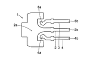
- FIG. 3 is a plan view for explaining the shape of a resin molding portion of the frame package shown in FIG. 1 (a view when viewed from the side on which the light emitting element is mounted).
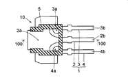
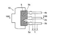
- FIG. 2 is a plan view for explaining the shape of a resin molding portion of the frame package shown in FIG. 1 (a view when viewed from the back side opposite to the side on which the light emitting element is mounted).
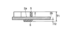
- FIG. 5 is a cross-sectional view taken along line 100-100 in FIGS. 3 and 4.
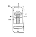
- FIG. 8 is a plan view of a state where a resin molding portion is molded in a portion to be a frame shown in FIG.
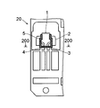
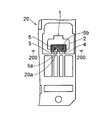
- FIG. 8 is a plan view of a state where a resin molding portion is molded in a portion to be a frame shown in FIG. 7 (a diagram when viewed from the back side opposite to the side on which the light emitting element is mounted).
- a frame package 10 manufactured using the method for manufacturing a frame package according to the present embodiment is for electrically connecting a semiconductor laser element 11 and an external device (not shown) as shown in FIG.
- the semiconductor laser element 11 mounted on the frame 1 is an example of the “light emitting element” in the present invention.
- the semiconductor laser element 11 shown in FIG. 1 is attached to the submount 12 by the junction down method, and the submount 12 is fixed to the frame 1 to be mounted on the frame 1. Yes.
- the semiconductor laser element 11 is a two-wavelength laser element, and the p-side electrode is separated into two and the n-side electrode is common.
- the p-side electrode and the n-side electrode of the semiconductor laser element 11 are electrically connected to the frame 1 through bonding wires 13. Since the p-side electrode of the semiconductor laser element 11 is electrically connected to the electrode pad formed on the submount 12, the p-side electrode bonding wire 13 is bonded to the electrode pad of the submount 12. .
- the frame 1 on which the semiconductor laser element 11 is mounted includes one main frame 2 and two sub frames 3 and 4, and these are electrically insulated from each other. It has a structure.
- the frame 1 is made of a metal thin plate (thin plate made of copper, iron, or the like) and is excellent in thermal conductivity and conductivity.
- the main frame 2 is an example of the “first frame” in the present invention
- the sub-frames 3 and 4 are examples of the “second frame” in the present invention.
- the main frame 2 is a frame on which the semiconductor laser element 11 is mounted and the n-side electrode of the semiconductor laser element 11 is electrically connected. That is, the main frame 2 has at least an element mounting portion 2a on which the semiconductor laser element 11 is mounted and an n-side electrode bonding wire 13 is bonded. A lead portion 2b connected to an external device is provided so as to extend integrally from the element mounting portion 2a of the main frame 2.
- the sub-frame 3 is a frame to which the p-side electrode (electrode pad of the submount 12) of the semiconductor laser element 11 is electrically connected, and a wire connection portion to which a bonding wire 13 for the p-side electrode is bonded. 3a and a lead portion (a portion connected to an external device) 3b extending integrally from the wire connection portion 3a.
- the subframe 4 also has a wire connection portion 4 a and a lead portion 4 b as in the subframe 3.
- the resin molded portion 5 has a shape as shown in FIG. 3 in a plan view from the side on which the semiconductor laser element 11 is mounted (hereinafter referred to as the element mounting side). More specifically, the part on the element mounting side of the resin molding portion 5 surrounds the element mounting area and the area including the peripheral area from three directions when viewed in plan, and the semiconductor laser element 11 (see FIG. 1).
- the light emitting side is substantially U-shaped open.
- an opening 5 a that straddles the main frame 2 and the subframe 3 is formed in a portion on the back surface side of the resin molded portion 5. A part of the surface on the back side of each of the main frame 2 and the sub-frame 3 is exposed from the opening 5a.
- a circular opening 5 b is formed in a portion on the back surface side of the resin molding portion 5 so as to expose a part of the surface on the back surface side of the sub-frame 4.
- the total thickness T1 of the resin molded portion 5 is about 1.5 mm to about 1.6 mm, and the thickness T2 of the back side portion of the resin molded portion 5 is about 0.2 mm. . That is, the thickness of the portion on the back surface side of the resin molded portion 5 is smaller than that of the conventional one.
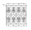
- a metal structure 20 in which a plurality of frames 1 (the hatched portions in FIGS. 6 and 7) are integrally connected is manufactured.
- Such a metal structure 20 can be obtained by, for example, pressing (punching) a metal thin plate such as a copper thin plate.
- FIGS. 8 and 9 show a predetermined portion of the frame 1 when viewed from the element mounting side
- FIG. 9 shows the planar shape of the resin molded portion 5 when viewed from the back side opposite to the element mounting side. is there.
- the mold 31 is disposed on the back side opposite to the element mounting side, and the mold 32 is disposed on the element mounting side. Is.
- the pair of molds 31 and 32 included in the molding mold 30 are examples of the “first mold” and the “second mold” of the present invention, respectively.
- the structure of the molding die 30 used in the insert molding step is a cavity (resin molding part 5 (see FIGS. 8 and 9)) by clamping the pair of dies 31 and 32. 30a) is formed.
- the space 30a is formed to reflect the shape of the above.
- the mold 31 of the pair of molds 31 and 32 is provided with a gate 31a for injecting molten resin to be the resin molding portion 5 into the cavity 30a.
- the gate 31a is formed on the cavity surface of the mold 31 opposite to the cavity surface of the other mold 32 (the bottom surface of the cavity recess formed in the other mold 32). Provided in a predetermined portion of the bottom surface) and protrudes into the cavity 30a.
- the gate 31a provided in the mold 31 is a region 20a in which the injection port 31b of the gate 31a does not overlap the frame 1 when viewed in plan when the molding die 30 to which the frame 1 is attached is clamped. That is, it is formed so as to be in the gap between the main frame 2 and the sub-frame 3 when seen in a plan view.
- the protruding height of the gate 31a is such that when the molding die 30 to which the frame 1 is attached is clamped, the outer edge surface 31c of the injection port 31b of the gate 31a is different from the surface of the frame 1 on the die 31 side.
- the height position of the outer edge surface 31c of the inlet 31b of the gate 31a is set to be substantially the same as the height position of the surface of the frame 1 on the mold 31 side.
- cross-sectional view of the molding die 30 shown in FIG. 10 represents the shape of the cavity 30a for resin molding of the cross-sectional portion along the line 200-200 in FIGS.
- the injection port 31b of the gate 31a is disposed in the gap between the main frame 2 and the sub frame 3 when viewed in plan. Further, the outer edge surface 31c of the inlet 31b of the gate 31a is in contact with a part of the surface of the main frame 2 and the sub frame 3 on the mold 31 side. That is, a part of the surface on the mold 31 side of each of the main frame 2 and the sub frame 3 is pressed by the outer edge surface 31c of the inlet 31b of the gate 31a, and the main frame 2 and the sub frame 3 are held. .
- the main frame 2 and the sub-frame are constituted by the gate 31a and a predetermined portion (a portion on which each of the main frame 2 and the sub-frame 3 is placed) facing the gate 31a.
- the frame 3 is clamped.
- a part of the surface of the sub frame 4 on the mold 31 side is held by a pressing pin (not shown).
- molten resin to be the resin molding portion 5 (see FIGS. 8 and 9) is injected from the gate 31a into the cavity 30a (in the direction of the arrow in FIG. 11). At this time, the molten resin flowing in the cavity 30 a is filled over the entire area of the cavity 30 a without being blocked by the frame 1. Then, after the molten resin is filled over the entire area in the cavity 30a, the molten resin filled in the cavity 30a is cured. Thereby, as shown in FIG. 12, the main frame 2 and the sub-frames 3 and 4 are fixed to each other by the resin molding portion 5.
- release is performed and the molded product is taken out.
- a burr 5c is generated along the injection port 31b of the gate 31a.
- the burr 5c protrudes from a height position substantially flush with the surface of the frame 1 on the mold 31 side.
- the outer edge surface 31c of the injection port 31b of the gate 31a presses and holds a part of the surface of each of the main frame 2 and the sub frame 3 on the mold 31 side, molding is performed from the back side opposite to the element mounting side.
- a part of the surface of each of the main frame 2 and the sub-frame 3 (the portion that is pressed and held by the outer edge surface 31c of the inlet 31b of the gate 31a (see FIG. 11)). Will be exposed. That is, the opening 5a is formed in the portion on the back surface side of the resin molding portion 5, and a part of the surface on the back surface side of each of the main frame 2 and the sub frame 3 is exposed from the opening 5a.
- another opening 5b formed in the portion on the back surface side of the resin molding portion 5 is formed by pressing and holding a part of the surface on the back surface side of the sub frame 4 by a pressing pin (not shown). Is. Therefore, a part of the surface on the back surface side of the sub-frame 4 is exposed from the opening 5 b of the resin molding portion 5.
- the frame package 10 shown in FIG. 1 is manufactured by separating the molded products individually.
- the gate 31a is placed in the region 20a that does not overlap the frame 1 when viewed in plan.
- the molding die 30 in which the injection port 31b is disposed and the outer edge surface 31c of the injection port 31b of the gate 31a is in contact with a part of the surface of the frame 1 on the mold 31 side.
- the depth of the cavity recess of the mold 31 can be made smaller than before without impairing the fluidity of the molten resin in the cavity 30a.
- the thickness of the part molded by the cavity recess of the mold 31 (the part on the back side of the resin molding part 5) can be made smaller than before, so that the frame package 10 can be made thinner. It becomes.
- the outer edge surface 31c of the inlet 31b of the gate 31a is used to A part of the surface on the mold 31 side is pressed and held, so that it is the same as a presser pin (a pin for suppressing misalignment or twisting of the frame 1) installed in the molding die 30. Since the gate 31a has the function, the number of presser pins installed in the molding die 30 can be reduced while reducing the thickness of the frame package 10.
- the frame package manufacturing method of the present embodiment when the frame 1 is mounted on the molding die 30 and clamped, the main frame 2 and the sub frame 3 are viewed in plan view.
- the injection port 31b of the gate 31a By arranging the injection port 31b of the gate 31a in the gap between them, the injection port 31b of the gate 31a can be easily arranged in a region that does not overlap with the frame 1 in plan view. it can.
- the main frame is arranged between the two sub-frames.
- the present invention is not limited to this, and the arrangement position of each frame can be changed as appropriate. That is, when there is one main frame and two sub frames, one of the two sub frames may be arranged in the center.
- the structure includes one main frame and two subframes.
- the present invention is not limited to this, and the number of frames can be changed as appropriate.
- a structure including one main frame and three sub frames may be used, and the sub frames may be arranged in the order of “sub frame, sub frame, main frame, sub frame”.
- the outer edge surface of the gate inlet may be brought into contact with the two subframes. In this way, it is possible to reduce the pressing pin for the sub frame.
Landscapes
- Physics & Mathematics (AREA)
- Condensed Matter Physics & Semiconductors (AREA)
- General Physics & Mathematics (AREA)
- Electromagnetism (AREA)
- Optics & Photonics (AREA)
- Engineering & Computer Science (AREA)
- Manufacturing & Machinery (AREA)
- Mechanical Engineering (AREA)
- Encapsulation Of And Coatings For Semiconductor Or Solid State Devices (AREA)
Abstract
【課題】薄型化を図ることが可能なフレームパッケージの製造方法を提供する。 【解決手段】このフレームパッケージの製造方法では、型締めした際に、平面的に見てフレーム1と重畳しない領域20aにゲート31aの注入口31bが配置され、かつ、その注入口31bの外縁面31cの高さ位置がフレーム1の金型31側の表面の高さ位置と略同じとなる成型用金型30を用いる。
Description
本発明は、発光素子が搭載されるフレームパッケージの製造方法に関する。
従来、発光素子としての半導体レーザ素子が搭載されるフレームパッケージが知られており、半導体レーザ素子と外部機器とを電気的に接続するために使用されている(たとえば、特許文献1参照)。
従来の半導体レーザ素子用のフレームパッケージは、一般的に、互いに電気的に絶縁された主フレームおよび副フレームからなるフレームを少なくとも備えている。そして、それら主フレームおよび副フレームは、樹脂成形部によって互いに固着された状態となっている。なお、主フレームは、半導体レーザ素子が搭載され、かつ、ボンディングワイヤを介して半導体レーザ素子の一方電極と電気的に接続されるフレームである。また、副フレームは、ボンディングワイヤを介して半導体レーザ素子の他方電極と電気的に接続されるフレームである。
また、上記した従来の半導体レーザ素子用のフレームパッケージは、たとえば、以下のような工程を経て製造される。
すなわち、まず、金属薄板に対してプレス加工を施すことによって、主フレームおよび副フレームからなるフレームが一体的に複数連結された金属構造体を作製する。次に、インサート成形を行うための成形用金型を準備し、その成型用金型を用いて樹脂成形部を成形することで、主フレームおよび副フレームが樹脂成形部によって互いに固着された状態にする。この後、成形品を個々に分離する。これにより、上記した従来の半導体レーザ素子用のフレームパッケージが得られる。
なお、インサート成形を行うための成形用金型は、互いに対向配置される一対の金型を含んでおり、その一対の金型を型締めすることによってキャビティ(樹脂成形部の形状を反映した形状を成す空間)が形成されるようになっている。また、一対の金型のうちの一方の金型には、樹脂成形部となる溶融樹脂をキャビティ内に注入するためのゲートが設けられている。
ところで、上記した従来のフレームパッケージの製造方法において、より薄型化されたフレームパッケージを得るには、キャビティの厚み(一方の金型のキャビティ用凹部の深さ)を小さくすることで樹脂成形部の厚みを小さくすればよいが、この場合には以下のような不都合が生じる。
すなわち、キャビティの厚みを単に小さくするだけでは、ゲートからキャビティ内に注入される溶融樹脂の流動がフレームによって阻害され、キャビティ内における溶融樹脂の流動性が低下してしまうという不都合がある。したがって、従来のフレームパッケージの製造方法では、フレームパッケージの薄型化を図るのが困難であるという問題がある。
本発明は、上記のような課題を解決するためになされたものであり、フレームパッケージ(樹脂成形部)の薄型化を図ることが可能なフレームパッケージの製造方法を提供することを目的とする。
上記の目的を達成するために、本発明の一の局面によるフレームパッケージの製造方法は、互いに電気的に絶縁された第1フレームおよび第2フレームからなるフレームを少なくとも備えているとともに、第1フレームおよび第2フレームが樹脂成形部によって互いに固着された構造を有し、フレームに発光素子が搭載されるフレームパッケージの製造方法であって、互いに対向配置される第1金型および第2金型を含み、第1金型および第2金型を型締めすることによってキャビティが形成され、かつ、キャビティ内に向かって突出するゲートが第1金型の第2金型と対向する所定部分に設けられた成形用金型を準備する工程と、フレームの樹脂成形部によって覆われる部分がキャビティ内に配置されるように、フレームを成形用金型に装着して型締めする工程と、樹脂成形部となる溶融樹脂をゲートからキャビティ内に注入し、キャビティ内の溶融樹脂を硬化させる工程とを備えている。そして、フレームを成形用金型に装着して型締めした際に、平面的に見てフレームと
重畳しない領域にゲートの注入口が配置され、かつ、そのゲートの注入口の外縁面の高さ位置がフレームの第1金型側の表面の高さ位置とほぼ同じとなるような成型用金型を用いる。
重畳しない領域にゲートの注入口が配置され、かつ、そのゲートの注入口の外縁面の高さ位置がフレームの第1金型側の表面の高さ位置とほぼ同じとなるような成型用金型を用いる。
この一の局面によるフレームパッケージの製造方法では、上記のように、フレームを成形用金型に装着して型締めした際に、平面的に見てフレームと重畳しない領域にゲートの注入口が配置され、かつ、そのゲートの注入口の外縁面の高さ位置がフレームの第1金型側の表面の高さ位置と略同じとなるような成型用金型を用いることによって、キャビティ内における溶融樹脂の流動性などを損なうことなく、第1金型のキャビティ用凹部の深さを従来よりも小さくすることができる。その結果、第1金型のキャビティ用凹部で成形される部分(樹脂成形部の第1金型側の部分)の厚みを従来よりも小さくすることができるので、フレームパッケージの薄型化を図ることが可能となる。
また、ゲートの注入口の外縁面の高さ位置がフレームの第1金型側の表面の高さ位置と略同じになっている状態で樹脂成形が行われるため、離型時にゲートの注入口に沿ったバリが発生したとしても、そのバリはフレームの第1金型側の表面と略面一の高さ位置から突出する。このため、フレームパッケージを薄型化することができることに加えて、バリが樹脂成形部よりも外側にはみ出してしまうのも抑制することができる。
なお、上記したフレームパッケージの製造方法では、フレームの第1金型側の表面にゲートの注入口の外縁面が接触していてもよいし、フレームの第1金型側の表面にゲートの注入口の外縁面が接触していなくてもよい。
上記一の局面によるフレームパッケージの製造方法において、フレームを成形用金型に装着して型締めした際に、ゲートの注入口の外縁面でフレームの第1金型側の表面の一部が押圧保持されることが好ましい。このようにすれば、成型用金型に設置される押えピン(フレームの位置ずれやねじれなどを抑制するためのピン)と同様の機能をゲートが持つことになるため、フレームパッケージの薄型化を図りながら、成形用金型に設置する押えピンの個数を減らすことができる。
上記一の局面によるフレームパッケージの製造方法において、フレームを成形用金型に装着して型締めした際に、平面的に見て第1フレームと第2フレームとの間の間隙にゲートの注入口が配置されることが好ましい。このようにすれば、容易に、平面的に見てフレームと重畳しない領域にゲートの注入口が配置された状態にすることができる。
この場合、第1フレームおよび第2フレームのそれぞれの第1金型側の表面の一部がゲートの注入口の外縁面で押圧保持されることが好ましい。このようにすれば、フレームの押圧保持を確実に行うことができる。これにより、フレームの位置ずれやねじれなどが抑制され、かつ、薄型化されたフレームパッケージを得ることができる。
以上のように、本発明によれば、容易に、フレームパッケージの薄型化を図ることができる。
まず、図1~図5を参照して、本実施形態によるフレームパッケージの製造方法を用いて製造されるフレームパッケージ10の構成について説明する。
本実施形態によるフレームパッケージの製造方法を用いて製造されるフレームパッケージ10は、図1に示すように、半導体レーザ素子11と外部機器(図示せず)とを電気的に接続するためのものであり、半導体レーザ素子11が搭載され、かつ、電気的に接続されるフレーム1を少なくとも備えている。このフレーム1に搭載される半導体レーザ素子11は、本発明の「発光素子」の一例である。
ところで、図1に示す半導体レーザ素子11は、ジャンクションダウン方式でサブマウント12に取り付けられており、そのサブマウント12がフレーム1に対して固着されることでフレーム1に搭載された状態となっている。また、半導体レーザ素子11は2波長レーザ素子であり、p側電極が2つに分離され、n側電極が共通となっている。そして、半導体レーザ素子11のp側電極およびn側電極は、ボンディングワイヤ13を介してフレーム1に電気的に接続されている。なお、半導体レーザ素子11のp側電極はサブマウント12に形成された電極パッドに電気的に接続されているため、p側電極用のボンディングワイヤ13はサブマウント12の電極パッドにボンディングされている。
ところで、図1に示す半導体レーザ素子11は、ジャンクションダウン方式でサブマウント12に取り付けられており、そのサブマウント12がフレーム1に対して固着されることでフレーム1に搭載された状態となっている。また、半導体レーザ素子11は2波長レーザ素子であり、p側電極が2つに分離され、n側電極が共通となっている。そして、半導体レーザ素子11のp側電極およびn側電極は、ボンディングワイヤ13を介してフレーム1に電気的に接続されている。なお、半導体レーザ素子11のp側電極はサブマウント12に形成された電極パッドに電気的に接続されているため、p側電極用のボンディングワイヤ13はサブマウント12の電極パッドにボンディングされている。
半導体レーザ素子11が搭載されるフレーム1は、図1および図2に示すように、1つの主フレーム2と2つの副フレーム3および4とを含んでいるとともに、それらが互いに電気的に絶縁された構造となっている。また、このフレーム1は、金属薄板(銅や鉄などからなる薄板)からなっており、熱伝導性および導電性に優れている。なお、主フレーム2は、本発明の「第1フレーム」の一例であり、副フレーム3および4は、本発明の「第2フレーム」の一例である。
主フレーム2は、半導体レーザ素子11が搭載され、かつ、半導体レーザ素子11のn側電極が電気的に接続されるフレームである。すなわち、主フレーム2は、半導体レーザ素子11が搭載され、かつ、n側電極用のボンディングワイヤ13がボンディングされる素子搭載部2aを少なくとも有している。そして、その主フレーム2の素子搭載部2aから一体的に延びるように、外部機器に接続されるリード部2bが設けられている。また、副フレーム3は、半導体レーザ素子11のp側電極(サブマウント12の電極パッド)が電気的に接続されるフレームであって、p側電極用のボンディングワイヤ13がボンディングされるワイヤ接続部3aと、そのワイヤ接続部3aから一体的に延びるリード部(外部機器に接続される部分)3bとを有している。なお、副フレーム4についても、副フレーム3と同様、ワイヤ接続部4aとリード部4bとを有している。
また、主フレーム2、副フレーム3および4は、樹脂成形部5によって互いに固着されている。この樹脂成形部5は、半導体レーザ素子11が搭載される側(以下、素子搭載側と言う)からの平面視において、図3に示すような形状となっている。具体的に言うと、樹脂成形部5の素子搭載側の部分は、平面的に見て、素子搭載領域およびその周辺領域を包含する領域を3方向から囲み、半導体レーザ素子11(図1参照)の光出射側が開放された略コの字形状になっている。
また、樹脂成形部5を素子搭載側とは反対の裏面側から見ると、図4に示すような形状となっている。なお、本実施形態によるフレームパッケージの製造方法を用いて製造すると、主フレーム2および副フレーム3を跨ぐような開口5aが樹脂成形部5の裏面側の部分に形成され、その樹脂成形部5の開口5aから主フレーム2および副フレーム3のそれぞれの裏面側の表面の一部が露出した状態となる。また、樹脂成形部5の裏面側の部分には、副フレーム4の裏面側の表面の一部を露出させるような円形状の開口5bも形成されている。
また、図5に示すように、樹脂成形部5の全体の厚みT1は約1.5mm~約1.6mmであり、樹脂成形部5の裏面側の部分の厚みT2は約0.2mmである。すなわち、樹脂成形部5の裏面側の部分の厚みは従来に比べて小さくなっている。
次に、図6~図13を参照して、本実施形態によるフレームパッケージの製造方法について説明する。
まず、図6および図7に示すように、複数のフレーム1(図6および図7のハッチングが施された部分)が一体的に連結された金属構造体20を作製する。このような金属構造体20は、たとえば、銅薄板などの金属薄板をプレス加工(打ち抜き加工)することで得られる。
金属構造体20を作製した後、図8および図9に示すように、フレーム1の所定部分を樹脂成形部5で覆い、主フレーム2、副フレーム3および4が樹脂成形部5によって互いに固着された状態にする。なお、図8は、素子搭載側から見た場合の樹脂成形部5の平面形状であり、図9は、素子搭載側とは反対の裏面側から見た場合の樹脂成形部5の平面形状である。
ところで、フレーム1の所定部分を樹脂成形部5で覆う工程(主フレーム2、副フレーム3および4を樹脂成形部5によって互いに固着する工程)では、互いに対向配置される一対の金型31および32を含む成型用金型30(図10参照)を準備し、その成型用金型30を用いてインサート成形を行う。この成型用金型30に含まれる一対の金型31および32のうちの金型31は素子搭載側とは反対の裏面側に配置されるものであり、金型32は素子搭載側に配置されるものである。なお、成型用金型30に含まれる一対の金型31および32は、それぞれ、本発明の「第1金型」および「第2金型」の一例である。
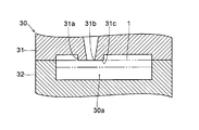
インサート成形工程で用いる成型用金型30の構造としては、図10に示すように、その一対の金型31および32を型締めすることによってキャビティ(樹脂成形部5(図8および図9参照)の形状を反映した形状を成す空間)30aが形成されるようになっている。また、一対の金型31および32のうちの金型31には、樹脂成形部5となる溶融樹脂をキャビティ30a内に注入するためのゲート31aが設けられている。このゲート31aは、他の金型32のキャビティ面(他の金型32に形成されたキャビティ用凹部の底面)と対向する金型31のキャビティ面(金型31に形成されたキャビティ用凹部の底面)の所定部分に設けられているとともに、キャビティ30a内に向かって突出している。
さらに、金型31に設けられたゲート31aは、フレーム1が装着された成型用金型30を型締めしたときに、ゲート31aの注入口31bが平面的に見てフレーム1と重畳しない領域20a(図7参照)、すなわち、平面的に見て主フレーム2と副フレーム3との間の間隙に来るように形成されている。また、そのゲート31aの突出高さは、フレーム1が装着された成型用金型30を型締めしたときに、ゲート31aの注入口31bの外縁面31cがフレーム1の金型31側の表面と略面一、すなわち、ゲート31aの注入口31bの外縁面31cの高さ位置がフレーム1の金型31側の表面の高さ位置と略同じになるように設定されている。
なお、図10に示す成型用金型30の断面図は、図8および図9の200-200線に沿った断面部分の樹脂成形を行うキャビティ30aの形状を表している。
そして、成型用金型30を用いてインサート成形を行う際には、図11に示すように、まず、フレーム1の樹脂成形部5(図8および図9参照)によって覆われる部分がキャビティ30a内に配置されるように、フレーム1を成型用金型30に装着して型締めする。
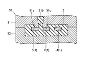
このとき、本実施形態では、平面的に見て主フレーム2と副フレーム3との間の間隙にゲート31aの注入口31bが配置された状態となる。さらに、ゲート31aの注入口31bの外縁面31cが主フレーム2および副フレーム3のそれぞれの金型31側の表面の一部に接触した状態となる。すなわち、主フレーム2および副フレーム3のそれぞれの金型31側の表面の一部がゲート31aの注入口31bの外縁面31cで押圧され、主フレーム2および副フレーム3が保持されることになる。具体的に言うと、ゲート31aと、そのゲート31aと対向する金型32の所定部分(主フレーム2および副フレーム3のそれぞれの一部が載置される部分)とによって、主フレーム2および副フレーム3が挟持される。なお、副フレーム4の金型31側の表面の一部は、図示しない押えピンで保持された状態となっている。
この後、樹脂成形部5(図8および図9参照)となる溶融樹脂をゲート31aからキャビティ30a内(図11の矢印方向)に注入する。この際、キャビティ30a内を流動する溶融樹脂は、フレーム1によって遮られることなく、キャビティ30a内の全域にわたって充填される。そして、キャビティ30a内の全域にわたって溶融樹脂が充填された後に、そのキャビティ30a内に充填された溶融樹脂を硬化させる。これにより、図12に示すように、主フレーム2、副フレーム3および4が樹脂成形部5によって互いに固着される。
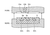
続いて、図13に示すように、離型を行い、成形品を取り出す。このとき、ゲート31aの注入口31bに沿ったバリ5cが発生するが、そのバリ5cはフレーム1の金型31側の表面と略面一の高さ位置から突出する。
また、ゲート31aの注入口31bの外縁面31cによって主フレーム2および副フレーム3のそれぞれの金型31側の表面の一部を押圧保持していたため、素子搭載側とは反対の裏面側から成形品を見ると、図9に示すように、主フレーム2および副フレーム3のそれぞれの表面の一部(ゲート31aの注入口31bの外縁面31c(図11参照)で押圧保持されていた部分)が露出された状態となる。すなわち、樹脂成形部5の裏面側の部分に開口5aが形成され、その開口5aから主フレーム2および副フレーム3のそれぞれの裏面側の表面の一部が露出される。なお、樹脂成形部5の裏面側の部分に形成される別の開口5bは、副フレーム4の裏面側の表面の一部が押えピン(図示せず)によって押圧保持されることで形成されるものである。したがって、樹脂成形部5の開口5bからは、副フレーム4の裏面側の表面の一部が露出される。
最後に、成形品を個々に分離することによって、図1に示したフレームパッケージ10が製造される。
本実施形態のフレームパッケージの製造方法では、上記のように、フレーム1を成形用金型30に装着して型締めした際に、平面的に見てフレーム1と重畳しない領域20aにゲート31aの注入口31bが配置され、かつ、そのゲート31aの注入口31bの外縁面31cがフレーム1の金型31側の表面の一部に接触した状態となるような成型用金型30を用いることによって、キャビティ30a内における溶融樹脂の流動性などを損なうことなく、金型31のキャビティ用凹部の深さを従来よりも小さくすることができる。その結果、金型31のキャビティ用凹部で成形される部分(樹脂成形部5の裏面側の部分)の厚みを従来よりも小さくすることができるので、フレームパッケージ10の薄型化を図ることが可能となる。
また、ゲート31aの注入口31bの外縁面31cがフレーム1の金型31側の表面の一部に接触した状態で樹脂成形が行われるため、離型時にゲート31aの注入口31bに沿ったバリ5cが発生したとしても、そのバリ5cはフレーム1の金型31側の表面と略面一の高さ位置から突出する。このため、フレームパッケージ10を薄型化できることに加えて、バリ5cが樹脂成形部5よりも外側にはみ出してしまうのも抑制することができる。
また、本実施形態のフレームパッケージの製造方法では、上記のように、フレーム1を成形用金型30に装着して型締めした際に、ゲート31aの注入口31bの外縁面31cでフレーム1の金型31側の表面の一部が押圧保持されるようにすることによって、成型用金型30に設置される押えピン(フレーム1の位置ずれやねじれなどを抑制するためのピン)と同様の機能をゲート31aが持つことになるため、フレームパッケージ10の薄型化を図りながら、成形用金型30に設置する押えピンの個数を減らすことができる。
さらに、本実施形態のフレームパッケージの製造方法では、上記のように、フレーム1を成形用金型30に装着して型締めした際に、平面的に見て主フレーム2と副フレーム3との間の間隙にゲート31aの注入口31bが配置されるようにすることによって、容易に、平面的に見てフレーム1と重畳しない領域にゲート31aの注入口31bが配置された状態にすることができる。
この場合、主フレーム2および副フレーム3のそれぞれの金型31側の表面の一部がゲート31aの注入口31bの外縁面31cで押圧保持されるようにすることによって、フレーム1の押圧保持を確実に行うことができる。これにより、フレーム1の位置ずれやねじれなどが抑制され、かつ、薄型化されたフレームパッケージ10を得ることができる。
今回開示された実施形態は、すべての点で例示であって制限的なものではないと考えられるべきである。本発明の範囲は、上記した実施形態の説明ではなく特許請求の範囲によって示され、さらに、特許請求の範囲と均等の意味および範囲内でのすべての変更が含まれる。
たとえば、上記実施形態では、2つの副フレームの間に主フレームを配置したが、本発明はこれに限らず、各フレームの配置位置は適宜変更可能である。すなわち、主フレームが1つで副フレームが2つの場合、2つの副フレームのうちの一方を中央に配置してもよい。
また、上記実施形態では、1つの主フレームと2つの副フレームとを含む構造としているが、本発明はこれに限らず、各フレームの個数は適宜変更可能である。たとえば、1つの主フレームと3つの副フレームとを含む構造とし、「副フレーム、副フレーム、主フレーム、副フレーム」の順番で配置してもよい。
また、2つの副フレームが連続して並ぶ場合には、ゲートの注入口の外縁面を2つの副フレームに接触させるようにしてもよい。このようにすれば、副フレーム用の押えピンを削減することができる。
1 フレーム
2 主フレーム(第1フレーム)
3、4 副フレーム(第2フレーム)
5 樹脂成形部
11 半導体レーザ素子(発光素子)
20a 領域
30 成型用金型
30a キャビティ
31 金型(第1金型)
31a ゲート
31b 注入口
31c 外縁面
32 金型(第2金型)
2 主フレーム(第1フレーム)
3、4 副フレーム(第2フレーム)
5 樹脂成形部
11 半導体レーザ素子(発光素子)
20a 領域
30 成型用金型
30a キャビティ
31 金型(第1金型)
31a ゲート
31b 注入口
31c 外縁面
32 金型(第2金型)
Claims (4)
- 互いに電気的に絶縁された第1フレームおよび第2フレームからなるフレームを少なくとも備えているとともに、前記第1フレームおよび前記第2フレームが樹脂成形部によって互いに固着された構造を有し、前記フレームに発光素子が搭載されるフレームパッケージの製造方法であって、
互いに対向配置される第1金型および第2金型を含み、前記第1金型および前記第2金型を型締めすることによってキャビティが形成され、かつ、前記キャビティ内に向かって突出するゲートが前記第1金型の前記第2金型と対向する所定部分に設けられた成形用金型を準備する工程と、
前記フレームの前記樹脂成形部によって覆われる部分が前記キャビティ内に配置されるように、前記フレームを前記成形用金型に装着して型締めする工程と、
前記樹脂成形部となる溶融樹脂を前記ゲートから前記キャビティ内に注入し、前記キャビティ内の前記溶融樹脂を硬化させる工程とを備え、
前記フレームを前記成形用金型に装着して型締めした際に、平面的に見て前記フレームと重畳しない領域に前記ゲートの注入口が配置され、かつ、前記ゲートの注入口の外縁面の高さ位置が前記フレームの前記第1金型側の表面の高さ位置と略同じとなるような成型用金型を用いることを特徴とするフレームパッケージの製造方法。 - 前記フレームを前記成形用金型に装着して型締めした際に、前記ゲートの注入口の外縁面で前記フレームの前記第1金型側の表面の一部が押圧保持されることを特徴とする請求項1に記載のフレームパッケージの製造方法。
- 前記フレームを前記成形用金型に装着して型締めした際に、平面的に見て前記第1フレームと前記第2フレームとの間の間隙に前記ゲートの注入口が配置されることを特徴とする請求項1または2に記載のフレームパッケージの製造方法。
- 前記第1フレームおよび前記第2フレームのそれぞれの前記第1金型側の表面の一部が前記ゲートの注入口の外縁面で押圧保持されることを特徴とする請求項3に記載のフレームパッケージの製造方法。
Applications Claiming Priority (2)
| Application Number | Priority Date | Filing Date | Title |
|---|---|---|---|
| JP2009-028589 | 2009-02-10 | ||
| JP2009028589 | 2009-02-10 |
Publications (1)
| Publication Number | Publication Date |
|---|---|
| WO2010092853A1 true WO2010092853A1 (ja) | 2010-08-19 |
Family
ID=42561700
Family Applications (1)
| Application Number | Title | Priority Date | Filing Date |
|---|---|---|---|
| PCT/JP2010/050489 Ceased WO2010092853A1 (ja) | 2009-02-10 | 2010-01-18 | フレームパッケージの製造方法 |
Country Status (1)
| Country | Link |
|---|---|
| WO (1) | WO2010092853A1 (ja) |
Cited By (1)
| Publication number | Priority date | Publication date | Assignee | Title |
|---|---|---|---|---|
| CN103358467A (zh) * | 2012-04-06 | 2013-10-23 | 矽品精密工业股份有限公司 | 用于封装半导体组件的铸模装置 |
Citations (8)
| Publication number | Priority date | Publication date | Assignee | Title |
|---|---|---|---|---|
| JPS6333916U (ja) * | 1986-08-21 | 1988-03-04 | ||
| JP2002043679A (ja) * | 2000-07-28 | 2002-02-08 | Sanyo Electric Co Ltd | 半導体レーザ装置 |
| JP2002086487A (ja) * | 2000-09-14 | 2002-03-26 | Teikoku Tsushin Kogyo Co Ltd | 基板の電極パターンへのモールド樹脂による端子板接続固定方法及び端子板付き電子部品 |
| JP2002223003A (ja) * | 2001-01-26 | 2002-08-09 | Nichia Chem Ind Ltd | パッケージ成形体とその製造方法及び発光装置 |
| JP2004363537A (ja) * | 2002-09-05 | 2004-12-24 | Nichia Chem Ind Ltd | 半導体装置およびその製造方法、並びにその半導体装置を用いた光学装置 |
| WO2005039000A1 (ja) * | 2003-10-15 | 2005-04-28 | Sanyo Electric Co., Ltd | 半導体レーザ装置 |
| JP2005539386A (ja) * | 2002-09-17 | 2005-12-22 | オスラム オプト セミコンダクターズ ゲゼルシャフト ミット ベシュレンクテル ハフツング | リードフレームをベースとしたハウジング、表面実装可能な光電構成素子及び製造法 |
| JP2008254275A (ja) * | 2007-04-03 | 2008-10-23 | Matsushita Electric Ind Co Ltd | 射出成形品と射出成形方法 |
-
2010
- 2010-01-18 WO PCT/JP2010/050489 patent/WO2010092853A1/ja not_active Ceased
Patent Citations (8)
| Publication number | Priority date | Publication date | Assignee | Title |
|---|---|---|---|---|
| JPS6333916U (ja) * | 1986-08-21 | 1988-03-04 | ||
| JP2002043679A (ja) * | 2000-07-28 | 2002-02-08 | Sanyo Electric Co Ltd | 半導体レーザ装置 |
| JP2002086487A (ja) * | 2000-09-14 | 2002-03-26 | Teikoku Tsushin Kogyo Co Ltd | 基板の電極パターンへのモールド樹脂による端子板接続固定方法及び端子板付き電子部品 |
| JP2002223003A (ja) * | 2001-01-26 | 2002-08-09 | Nichia Chem Ind Ltd | パッケージ成形体とその製造方法及び発光装置 |
| JP2004363537A (ja) * | 2002-09-05 | 2004-12-24 | Nichia Chem Ind Ltd | 半導体装置およびその製造方法、並びにその半導体装置を用いた光学装置 |
| JP2005539386A (ja) * | 2002-09-17 | 2005-12-22 | オスラム オプト セミコンダクターズ ゲゼルシャフト ミット ベシュレンクテル ハフツング | リードフレームをベースとしたハウジング、表面実装可能な光電構成素子及び製造法 |
| WO2005039000A1 (ja) * | 2003-10-15 | 2005-04-28 | Sanyo Electric Co., Ltd | 半導体レーザ装置 |
| JP2008254275A (ja) * | 2007-04-03 | 2008-10-23 | Matsushita Electric Ind Co Ltd | 射出成形品と射出成形方法 |
Cited By (1)
| Publication number | Priority date | Publication date | Assignee | Title |
|---|---|---|---|---|
| CN103358467A (zh) * | 2012-04-06 | 2013-10-23 | 矽品精密工业股份有限公司 | 用于封装半导体组件的铸模装置 |
Similar Documents
| Publication | Publication Date | Title |
|---|---|---|
| CN103219446B (zh) | 发光装置用封装成形体和使用了它的发光装置 | |
| JP4066608B2 (ja) | パッケージ成形体及びその製造方法 | |
| CN104347786B (zh) | 引线框、带树脂引线框、树脂封装体、发光装置以及树脂封装体的制造方法 | |
| JP5004601B2 (ja) | パッケージ部品の製造方法および半導体装置の製造方法 | |
| US20130011973A1 (en) | Leadframe strip and mold apparatus for an electronic component and method of encapsulating an electronic component | |
| CN105655318B (zh) | 半导体装置及其制造方法 | |
| JP2005123495A (ja) | 半導体装置の製造方法および半導体装置 | |
| JP2007165425A (ja) | 半導体装置 | |
| JP5246662B2 (ja) | 半導体装置用パッケージおよびその製造方法 | |
| JP2012059885A (ja) | 半導体装置の製造方法および半導体装置 | |
| JP7030481B2 (ja) | 樹脂封止金型および半導体装置の製造方法 | |
| JP6357415B2 (ja) | 半導体装置の製造方法 | |
| JP2009194212A (ja) | パワーモジュール構造 | |
| KR100591718B1 (ko) | 수지-밀봉형 반도체 장치 | |
| JP5136458B2 (ja) | 半導体パッケージ及びその製造方法 | |
| KR20200007688A (ko) | 수지 봉지 금형 및 반도체 장치의 제조 방법 | |
| JP3185996U (ja) | リードフレームアセンブリ | |
| JP2017152496A (ja) | リードフレーム、及び半導体パッケージの製造方法 | |
| JP5923293B2 (ja) | モールド金型 | |
| JP2011238963A (ja) | パッケージ部品の製造方法 | |
| JP2604054B2 (ja) | 半導体装置の製造方法 | |
| JP6825660B2 (ja) | リードフレーム、樹脂付きリードフレーム、樹脂パッケージ、発光装置及び樹脂パッケージの製造方法 | |
| KR20100032083A (ko) | 사이드뷰 led 패키지 및 그것의 몸체를 성형하기 위한 금형 세트 및 방법 | |
| WO2010098156A1 (ja) | フレームパッケージ型発光装置およびその製造方法 | |
| JPH0824156B2 (ja) | 樹脂封止型半導体装置の製造方法 |
Legal Events
| Date | Code | Title | Description |
|---|---|---|---|
| 121 | Ep: the epo has been informed by wipo that ep was designated in this application |
Ref document number: 10741133 Country of ref document: EP Kind code of ref document: A1 |
|
| NENP | Non-entry into the national phase |
Ref country code: DE |
|
| 122 | Ep: pct application non-entry in european phase |
Ref document number: 10741133 Country of ref document: EP Kind code of ref document: A1 |
|
| NENP | Non-entry into the national phase |
Ref country code: JP |