WO2010082268A1 - アナログデジタル変換方法、及びアナログデジタル変換装置 - Google Patents
アナログデジタル変換方法、及びアナログデジタル変換装置 Download PDFInfo
- Publication number
- WO2010082268A1 WO2010082268A1 PCT/JP2009/006677 JP2009006677W WO2010082268A1 WO 2010082268 A1 WO2010082268 A1 WO 2010082268A1 JP 2009006677 W JP2009006677 W JP 2009006677W WO 2010082268 A1 WO2010082268 A1 WO 2010082268A1
- Authority
- WO
- WIPO (PCT)
- Prior art keywords
- analog
- correction
- group
- signal
- digital
- Prior art date
- Legal status (The legal status is an assumption and is not a legal conclusion. Google has not performed a legal analysis and makes no representation as to the accuracy of the status listed.)
- Ceased
Links
Images


Classifications
-
- H—ELECTRICITY
- H03—ELECTRONIC CIRCUITRY
- H03M—CODING; DECODING; CODE CONVERSION IN GENERAL
- H03M1/00—Analogue/digital conversion; Digital/analogue conversion
- H03M1/10—Calibration or testing
- H03M1/1009—Calibration
- H03M1/1033—Calibration over the full range of the converter, e.g. for correcting differential non-linearity
-
- H—ELECTRICITY
- H03—ELECTRONIC CIRCUITRY
- H03M—CODING; DECODING; CODE CONVERSION IN GENERAL
- H03M1/00—Analogue/digital conversion; Digital/analogue conversion
- H03M1/12—Analogue/digital converters
- H03M1/1205—Multiplexed conversion systems
- H03M1/121—Interleaved, i.e. using multiple converters or converter parts for one channel
- H03M1/1215—Interleaved, i.e. using multiple converters or converter parts for one channel using time-division multiplexing
Definitions
- the present invention relates to an analog-digital conversion method for converting an analog signal into a digital signal, and an analog-digital conversion apparatus.
- the phase of the sampling clock given to each ADC needs to be different by a predetermined phase, but it is difficult to accurately shift the phase of each sampling clock by a predetermined phase.
- Even when the sampling clock is given to each ADC with an accurate phase if the ADC frequency characteristics are not ideal, the sampling timing or gain in each ADC varies, and the frequency spectrum of the digital signal Is difficult to calculate accurately.
- an object of one aspect of the present invention is to provide an analog-to-digital conversion method and an analog-to-digital converter that can solve the above-described problems. This object is achieved by a combination of features described in the independent claims.
- the dependent claims define further advantageous specific examples of the present invention.
- an analog-to-digital conversion method for converting an analog signal into a digital signal by using a plurality of analog-digital converters each having a predetermined sampling clock phase different from each other by a predetermined period.
- a measurement stage that measures the frequency characteristics of analog-digital converters in advance, a sampling stage that samples analog signals using multiple analog-digital converters, and a Fourier transform of the data sampled by multiple analog-digital converters, respectively.
- a Fourier transform stage that generates a plurality of measurement signals corresponding to the digital converter, and for each measurement signal divided into a plurality of groups, all analog digitals in the group to which the measurement signal belongs.
- An analog-to-digital conversion method includes an inter-group correction stage that corrects and synthesizes the frequency characteristics of each group based on the frequency characteristic difference between the groups, and generates a frequency spectrum of the digital signal.
- an analog-to-digital conversion device for converting an analog signal into a digital signal, wherein a plurality of analog-digital converters each having a predetermined sampling clock phase different from each other and the respective analog-digital converters
- a measurement unit that measures the frequency characteristics of the converter in advance
- a Fourier transform unit that generates a plurality of measurement signals corresponding to a plurality of analog-digital converters by Fourier-transforming data obtained by sampling analog signals by a plurality of analog-digital converters, For each group in which multiple measurement signals are divided into multiple groups, each measurement signal is multiplied by a correction coefficient based on the frequency characteristics of all analog-digital converters in the group to which the measurement signal belongs.
- an analog-to-digital converter comprising an inter-group correction unit that corrects frequency characteristics and an interleaving unit that synthesizes respective ideal measurement signals and generates a frequency spectrum of a digital signal.
- FIG. 10 is a flowchart illustrating an example of the operation of the interleaved AD conversion device 100 illustrated in FIG. 9. It is a figure which shows the other example of a structure of the interleave AD conversion apparatus. It is a flowchart which shows an example of operation
- FIG. 1 is a diagram illustrating an example of a configuration of an interleaved AD conversion apparatus 100 according to an embodiment of the present invention.
- the interleave AD conversion apparatus 100 converts an analog signal given as an input signal into a digital signal, and includes a plurality of ADCs (10-0 to 10-3, hereinafter collectively referred to as ADC10), and a plurality of Fourier transform units. (12-0 to 12-3, hereinafter collectively referred to as Fourier transform unit 12), a plurality of correction units (16-0 to 16-3, hereinafter collectively referred to as correction unit 16), measurement unit 14, and interleave unit 18 Prepare.
- the interleaved AD converter 100 uses four ADCs 10 to convert an analog signal into a digital signal, but the number of ADCs 10 is not limited to four.
- the interleave AD converter 100 may convert an analog signal into a digital signal by using 2 n (where n is an integer of 1 or more) ADCs 10. Even in such a case, the frequency spectrum of the digital signal can be accurately calculated by the same operation as that of the interleaved AD conversion apparatus 100 in this example.
- Each ADC 10 is provided with a sampling clock whose phase is different by a predetermined phase.
- the given sampling clock will be described later with reference to FIG.
- An analog signal is supplied to the ADC 10 as an input signal, and the analog signal is sampled according to the sampling clock.
- Each Fourier transform unit 12 is provided corresponding to the ADC 10, and each of the data obtained by sampling the analog signal by the plurality of ADCs 10 is Fourier transformed to generate a plurality of measurement signals corresponding to the plurality of ADCs 10.
- the Fourier transform unit 12 performs Fourier transform, for example, by discrete Fourier transform.
- the measuring unit 14 measures the frequency characteristics of each ADC 10 in advance. For example, the measurement unit 14 inputs a known analog signal to each ADC 10 and measures the frequency characteristics of each ADC 10 based on data output from the ADC 10. At this time, the measurement unit 14 may measure each frequency characteristic using a sampling clock given when converting an analog signal into a digital signal. For example, when measuring the frequency characteristics of each ADC 10, a sampling clock used in actual operation may be given to each ADC 10 and the output of each ADC 10 may be measured. Thereby, the frequency characteristics of sampling in each ADC 10 including the phase error of the given sampling clock can be measured.
- the correction unit 16 multiplies each measurement signal by a correction coefficient based on the frequency characteristics of all the ADCs 10 to convert them into ideal measurement signals obtained when the corresponding ADC 10 has ideal frequency characteristics.
- the frequency characteristic of any one ADC 10 may be the ideal frequency characteristic.
- the interleave unit 18 synthesizes each ideal measurement signal and generates a frequency spectrum of the digital signal. With such a configuration, it is possible to obtain a frequency spectrum from which spurious components generated by the sampling frequency characteristics in the ADC 10 are removed.
- FIG. 2 is a diagram for explaining a sampling clock given to each ADC 10.
- each ADC 10 has a sampling clock having a frequency of 1 / (4Ts) by phase Ts. Given off. By sampling an analog signal using such a sampling clock, the analog signal can be sampled at a rate four times the sampling frequency of each ADC 10.
- FIG. 3 is a diagram illustrating an example of frequency characteristics output from each Fourier transform unit 12.
- the measurement signal obtained by sampling the analog signal of the band [ ⁇ 1 / (2Ts), 1 / (2Ts)] at the frequency 1 / (4Ts) is spurious.
- FIG. 4 shows an example of a part of the frequency characteristic output from the Fourier transform unit 12-1.
- FIG. 5 is a diagram showing an example in which each frequency characteristic is displayed in a complex space.
- the signal component and the spurious component are shown discretely, but the same is true even if the band of the signal component and the spurious component overlap as in the frequency characteristics shown in FIG.
- the frequency characteristic components output from the Fourier transform unit 12-1 are sequentially rotated by 90 degrees. Further, since the phase of the sampling clock of the ADC 10-2 is advanced by 2Ts compared with the phase of the sampling clock of the ADC 10-0, the frequency characteristic component output by the Fourier transform unit 12-2 is 180 as shown in FIG. Rotate by degrees. Similarly, the phase of the sampling clock of the ADC 10-3 is advanced by 3Ts compared to the phase of the sampling clock of the ADC 10-0. Therefore, the frequency characteristic component output by the Fourier transform unit 12-3 is as shown in FIG. Rotate by 270 degrees.
- FIG. 6 shows another example of part of the frequency characteristics output from the Fourier transform unit 12-1.
- the interleave AD conversion apparatus 100 described in FIG. 1 removes spurious components by performing interleaving by correcting such angular variations of spurious components caused by the frequency characteristics of the ADC 10 or the phase error of the sampling clock. Next, details of the operation of the interleaved AD converter 100 will be described.
- FIG. 7 is a flowchart showing an example of the operation of the interleaved AD converter 100.
- the measurement unit 14 measures the frequency characteristics of each ADC 10 in advance.
- the frequency characteristic of each ADC 10 is given by the following equation.
- sampling clocks p 0 (t), p 1 (t), p 2 (t), and p 3 (t) given to each ADC 10 are given by the following equations. ... Formula (1)
- the Fourier transform unit 12 is used to Fourier-transform the data sampled by the plurality of ADCs 10 to generate a plurality of measurement signals corresponding to the plurality of ADCs 10.
- the Fourier transform of the sampling clock shown in Expression (1) is given by the following expression. ... Formula (2)
- each measurement signal can be expressed as follows.
- the correction unit 16 is used to multiply each measurement signal by a correction coefficient based on the frequency characteristics of all the ADCs 10, thereby obtaining the case where the frequency characteristics of the corresponding ADCs 10 are ideal. Converted to a measured signal.
- Correction coefficients L 1 , L 2 and L 3 are calculated and multiplied by their frequency characteristics.
- ⁇ and ⁇ are arbitrary real numbers.
- the correction unit 16 divides the frequency band [ ⁇ 2 fs, 2 fs] of the digital signal to be calculated according to the number of ADCs 10.
- the correction unit 16 determines the frequency band of the digital signal to be calculated as a first area where the band is [0, fs], a second area where the band is [fs, 2fs], and a band is [2fs, 3fs. ] And a fourth area whose band is [3fs, 4fs].
- amendment part 16 can calculate each correction coefficient for every frequency band, as shown in the following Formula. 1st area ... Formula (6) Second region and third region ... Formula (7) 4th area ... Formula (8)
- the interleave unit 18 is used to synthesize the respective measurement signals obtained in the correction step S206 to generate a frequency spectrum of the digital signal.
- the correction step S206 includes a first calculation step for calculating the first correction coefficient and a second calculation step for calculating the second correction coefficient.
- the respective first correction coefficients L 1 , L 2 , and L 3 multiplied by the respective measurement signals are calculated so that the spurious components of the respective measurement signals generated by the frequency characteristics of the respective ADCs 10 cancel out.
- the first correction coefficients L 1 , L 2 , and L 3 that cancel out the spurious components existing in the respective regions obtained by dividing the frequency band among the spurious components of the respective frequency signals are calculated as follows: Calculation is performed for each of the divided areas.
- the combination of the respective measurement signals obtained in the correction step S206 is multiplied by the second correction coefficient described above.
- the second correction coefficient is multiplied in the synthesis step S208.
- the second correction coefficient may be multiplied in the correction step S206. That is, in the correction step S206, each measurement signal may be multiplied by the corresponding first correction coefficient and the corresponding second correction coefficient.
- the frequency spectrum of the digital signal is calculated for each region based on the following equation.
- the frequency spectrum in the second region is calculated by using the correction coefficients L 1 , L 2 , and L 3 calculated based on Equation (7) in Equation (9), and the frequency spectrum in the third region is
- the correction coefficients L 1 , L 2 , and L 3 calculated based on Expression (7) are calculated by using Expression (10), and the frequency spectrum in the fourth region is calculated based on Expression (8).
- Calculation is performed by using the correction coefficients L 1 , L 2 , and L 3 in Expression (10). By such an operation, a frequency spectrum from which spurious components are removed can be obtained.
- the frequency characteristic of the ADC 10-0 is described as an ideal frequency characteristic. However, even when the frequency characteristic of the ADC 10-0 is not ideal and has a certain frequency characteristic, Correction can be performed based on the frequency characteristics to remove spurious components.
- the given analog signal has been described as a complex signal.
- the given analog signal is a real signal
- only the operations corresponding to the first region and the second region are applied among the correction methods described above.
- the frequency spectrum in the first region and the second region is calculated by using the correction coefficient calculated based on the equation (6) or the equation (7) in the equation (9), and the first region
- the complex conjugate of the frequency spectrum in the second region is calculated as the frequency spectrum in the third region and the fourth region.
- the frequency spectrum band to be calculated is described as [0, 4fs], but the same operation can be performed even when the band is set to [-2fs, 2fs].
- the band of the third area is set to [ ⁇ fs, 0]
- the band of the fourth area can be removed by the same operation.
- the number of ADCs 10 is described as four. However, even if the number of ADCs 10 is N (where N is an integer of 2 or more), a frequency spectrum from which spurious components are removed can be calculated in the same manner.
- N is an integer of 2 or more
- Formula (4), Formula (5), Formula (9), and Formula (10) are expressed as follows:
- the interleave unit 18 outputs a frequency domain signal in a band from 0 to f. For this reason, it is preferable that the correction unit 16 performs correction by compensating for the above-described band difference.
- FIG. 8A is a diagram illustrating an example of band compensation in the correction unit 16.
- the signal component and its image component are indicated by a solid line, and these complex conjugate components are indicated by a broken line.
- each correction unit 16 receives a frequency domain signal in a band from 0 to f / 4.
- An image component appears in the band from f / 2 to 3f / 4.
- the correction unit 16 generates a complex conjugate component for the frequency domain signal and the image component.
- the correction unit 16 copies each complex conjugate component so as to be a mirror image with the signal component with f / 4 and 3f / 4 as boundaries. Thereby, a frequency domain signal in a band from 0 to f can be generated.
- the correction unit 16 may perform the correction described with reference to FIGS. 1 to 7 on the frequency domain signal whose band is compensated. By synthesizing the frequency domain signal corrected by the correction unit 16 by the interleaving unit 18, a signal in a band from 0 to f can be generated.
- FIG. 8B is a diagram illustrating another example of band compensation in the correction unit 16.
- the correction unit 16 of the present example generates a complex conjugate component for a frequency domain signal in a band from 0 to f / 4. Then, the correction unit 16 copies each complex conjugate component so as to be a mirror image with the signal component with f / 4 as a boundary. As a result, a frequency domain signal in a band from 0 to f / 2 can be generated.
- the correction unit 16 may perform the correction described with reference to FIGS. 1 to 7 on the frequency domain signal whose band is compensated.
- the interleave unit 18 further compensates the band.
- FIG. 8C is a diagram illustrating an example of band compensation in the interleave unit 18 after the band compensation in the correction unit 16 described with reference to FIG. 8B.
- each correction unit 16 outputs a frequency domain signal in a band from 0 to f / 2.
- the interleave unit 18 combines these frequency domain signals to generate a combined signal in a band from 0 to f / 2.
- the interleave unit 18 copies the complex conjugate component of the combined signal so that it becomes a mirror image with the signal component with f / 2 as a boundary.
- a combined signal in a band from 0 to f can be generated.
- FIG. 9 is a diagram illustrating another example of the configuration of the interleaved AD conversion apparatus 100.
- the interleaved AD converter 100 of this example includes a plurality of ADCs (10-0 to 10-7), a plurality of Fourier transform units (12-0 to 12-7), and a plurality of intra-group correction units (20-0 to 20). -1), an inter-group correction unit 30 and a measurement unit 14 are provided.
- the ADC 10, the Fourier transform unit 12, and the measurement unit 14 have the same functions as the ADC 10, the Fourier transform unit 12, and the measurement unit 14 described with reference to FIG. 1.
- the intra-group correction unit 20 is provided for each group obtained by dividing a plurality of measurement signals into a plurality of groups. Each intra-group correction unit 20 performs the correction described with reference to FIGS. 1 to 7 on the corresponding group of measurement signals. That is, each intra-group correction unit 20 multiplies each measurement signal by a correction coefficient based on the frequency characteristics of all ADCs 10 in the group to which the corresponding ADC 10 has an ideal frequency characteristic. Convert to the resulting measurement signal. Each intra-group correction unit 20 may receive the frequency characteristic of the corresponding ADC 10 from the measurement unit 14.
- each intra-group correction unit 20 calculates the first correction coefficient L described in relation to Expression (5) to Expression (8) for the corresponding group. Further, each intra-group correction unit 20 calculates the second correction coefficient described in relation to Expression (9) and Expression (10) for the corresponding group. Then, each intra-group correction unit 20 performs the correction described in relation to Expression (9) and Expression (10) for the corresponding group using the first correction coefficient and the second correction coefficient. Further, the intra-group correction unit 20 may synthesize and output a plurality of corrected measurement signals as described in relation to the equations (9) and (10).
- each of the intra-group correction units 20 performs the correction described with reference to FIGS. 1 to 7, so that the plurality of measurement signals are divided into groups each including a power-of-two measurement signal. It is preferable.
- the plurality of measurement signals are preferably divided into groups each including the same number of measurement signals.
- the plurality of measurement signals are preferably divided so that the relative phase difference between the plurality of measurement signals is uniform within the group and is equal between the groups.
- the plurality of measurement signals include groups corresponding to ADCs 10-0, 10-4, 10-2, and 10-6, and groups corresponding to ADCs 10-1, ADC10-5, ADC10-3, and ADC12-7. And divided.
- the ADC 10-0 to ADC 10-7 are supplied with a sampling clock whose phase is shifted by a predetermined value as in the example shown in FIG. For example, if the sampling clock period is 8Ts, the ADC 10-m is given a sampling clock whose phase is delayed by m ⁇ Ts with respect to the sampling clock of the ADC 10-0.
- the sampling clock period is 8Ts
- the ADC 10-m is given a sampling clock whose phase is delayed by m ⁇ Ts with respect to the sampling clock of the ADC 10-0.
- each intra-group correction unit 20 may correct the measurement signal in the group on the basis of the frequency characteristic of any one of the ADCs 10 included in the corresponding group.
- the intra-group correction unit 20-0 uses the measurement signal corresponding to the ADC 10-0 as a reference
- the intra-group correction unit 20-1 uses the measurement signal corresponding to the ADC 10-1 as a reference.
- the inter-group correction unit 30 corrects and synthesizes the frequency characteristics of the respective groups based on the frequency characteristic difference between the groups corrected by the respective intra-group correction units 20, and generates a frequency spectrum of the digital signal. .
- the inter-group correction unit 30 may correct the frequency characteristics of each group based on the frequency characteristics of any group.
- the inter-group correction unit 30 may correct the frequency characteristics of each group on the basis of the group frequency characteristics of the intra-group correction unit 20-0.
- the group of the intra-group correction unit 20-0 matches the frequency characteristic of the ADC 10-0
- the group of the intra-group correction unit 20-1 matches the frequency characteristic of the ADC 10-1.
- the inter-group correction unit 30 may correct the measurement signal of each group based on the frequency characteristics of the ADC 10-0 and the ADC 10-1.
- the inter-group correction unit 30 may be given from the measurement unit 14 the frequency characteristics of the ADC 10 used as a reference in each intra-group correction unit 20.
- the inter-group correction unit 30 uses the signal output from the intra-group correction unit 20 as one measurement signal, and corrects the signal output from each intra-group correction unit 20 by the method described with reference to FIGS. 1 to 7. It's okay. Even with such a configuration, it is possible to generate a signal in which the frequency characteristic difference between the plurality of ADCs 10 is compensated. In addition, in the method described with reference to FIGS. 1 to 7, an N ⁇ 1-dimensional matrix operation must be performed to calculate the first correction coefficient and the second correction coefficient (where N is the ADC 10). Number).
- the intra-group correction unit 20 performs (N / k) -1 dimensional matrix calculation (where k is the number of divisions), and the inter-group correction unit 30 performs k ⁇ A one-dimensional matrix operation may be performed. For this reason, the order of matrix operation can be reduced, and the correction coefficient can be calculated by simple calculation.
- FIG. 10 is a flowchart showing an example of the operation of the interleaved AD converter 100 shown in FIG.
- the interleaved AD conversion apparatus 100 of this example first performs the operations from S200 to S204 described with reference to FIG.
- the intra-group correction unit 20 corrects the measurement signal included in each group.
- the processing of S206 and S208 described in relation to FIG. 7 may be performed in each group.
- the inter-group correction unit 30 corrects the measurement signal based on the frequency characteristic difference between the groups.
- the processing of S206 and S208 may be performed using the output of each intra-group correction unit 20 as one measurement signal. By such an operation, the frequency characteristic difference can be compensated by a simple process.
- FIG. 11 is a diagram illustrating another example of the configuration of the interleaved AD conversion apparatus 100.
- the interleaved AD conversion apparatus 100 of this example has a plurality of correction stages, and corrects the frequency characteristic difference for every two channels in each correction stage.
- the intra-group correction unit 20 may function as the first correction stage
- the inter-group correction unit 30 may function as the subsequent correction stage.
- the interleave AD conversion apparatus 100 of this example includes one intra-group correction unit 20 for every two ADCs 10. For this reason, the intra-group correction unit 20 divides the plurality of measurement signals into groups for each of the two measurement signals, and corrects the frequency characteristic difference.
- each intra-group correction unit 20 is associated with each ADC 10 so that the relative phase difference of the corresponding pair of ADCs 10 is the same as the other pairs.
- the ADCs 10 are paired so that the relative phase difference (4 Ts in this example) of each pair of ADCs 10 is approximately half of the sampling clock period (8 Ts in this example).
- the pairing of the ADC 10 may be determined based on a result of representing an integer in a binary number and reversing the bit sequence horizontally. For example, the integers 0 and 1 in binary notation are 000 and 001. If this is bit-reversed, 000 and 100 are obtained. Since the binary number represents integers 0 and 4, the intra-group correction unit 20-0 is associated with a pair of ADC 10-0 and ADC 10-4.
- integers 2 and 3 represented in binary are 010 and 011. When this is bit-reversed, 010 and 110 are obtained. Since the binary number represents integers 2 and 6, the intra-group correction unit 20-2 is associated with the ADC 10-2 and the ADC 10-6. Similarly, the ADC 10-1 and ADC 10-5 are associated with the intra-group correction unit 20-1, and the ADC 10-3 and ADC 10-7 are associated with the intra-group correction unit 20-3.
- Each intra-group correction unit 20 may correct each measurement signal based on the frequency characteristics of the ADC 10 corresponding to any one of the measurement signals.
- Each intra-group correction unit 20 is given the frequency characteristic of the corresponding ADC 10 from the measurement unit 14.
- the processing in the intra-group correction unit 20 may be the same as the case where the number of ADCs 10 is 2 in the processing described with reference to FIGS.
- the inter-group correction unit 30 divides the group output by each intra-group correction unit 20 into corresponding group pairs, and determines the frequency characteristics of each group pair based on the frequency characteristic difference in each group pair. It correct
- the inter-group correction unit 30 includes a plurality of stages of correction units.
- the inter-group correction unit 30 of this example includes a plurality of first correction units 32 and second correction units 34 provided in two stages.
- Each first correction unit 32 receives the outputs of the corresponding two in-group correction units 20 and corrects them based on the frequency characteristic difference between the corresponding ADCs 10.
- the first correction unit 32-0 is based on the frequency characteristics of the ADC 10-0 that is referenced by the intra-group correction unit 20-0 and the ADC 10-2 that is referenced by the intra-group correction unit 20-2.
- the signal output from the intra-group correction unit 20 is corrected.
- the processing in the first correction unit 32 may be the same as the case where the number of ADCs 10 is 2 in the processing described with reference to FIGS. Which in-group correction unit 20 is associated with each first correction unit 32 may be determined under the same conditions as the pairing of the ADC 10.
- the second correction unit 34 receives the outputs of the two first correction units 32 and corrects them based on the frequency characteristic difference between the corresponding ADCs 10.
- the processing in the second correction unit 34 may be the same as the case where the number of ADCs 10 is 2 in the processing described with reference to FIGS.
- the matrix operation in each correction unit can be a one-dimensional matrix operation. For this reason, the frequency characteristic difference can be compensated for by simple processing.
- a correction unit having the same configuration may be designed. In this case, the correction coefficient used in each correction unit is set independently.
- each correction unit calculates a correction coefficient by dividing the frequency domain into two.
- the boundary between the regions becomes the Nyquist frequency, and thus the divided regions have a complex conjugate relationship. That is, for each region, the correction coefficients calculated according to the equations (5) to (10) are the same.
- the interleave AD conversion apparatus 100 of this example may calculate the correction coefficient without dividing the frequency domain for each correction unit.
- the correction coefficient calculated for one of the divided frequency regions may be used in the other frequency region. For this reason, the frequency characteristic difference can be compensated by a simpler process.
- FIG. 12 is a flowchart showing an example of the operation of the interleaved AD converter 100 shown in FIG.
- the interleaved AD conversion apparatus 100 of this example first performs the operations from S200 to S204 described with reference to FIG.
- the intra-group correction unit 20 corrects and synthesizes the two paired measurement signals based on the frequency characteristics of the corresponding ADC 10.
- the correction step S214 for each pair, two ADCs 10 are used to multiply the first correction coefficient by multiplying one of the measurement signals so that the spurious components of the respective measurement signals generated by the frequency characteristics of the respective ADCs 10 cancel each other.
- the first correction coefficient L1 may be calculated based on the following equation. ... Formula (11)
- a M (1) indicates a component corresponding to a spurious component in the frequency characteristics of the ADC 10 corresponding to the measurement signal multiplied by the first correction coefficient.
- the second correction coefficient ⁇ for correcting the phase error of the signal component of the measurement signal which is generated by multiplying the first correction coefficient for each pair, is set as the first correction coefficient L1 and the respective correction coefficients S1.
- Calculation is based on the frequency characteristics of the ADC 10.
- the correction coefficient ⁇ may be calculated based on the following equation. ... Formula (12)
- a M (0) indicates a component corresponding to the signal component in the frequency characteristics of the ADC 10 corresponding to the measurement signal multiplied by the first correction coefficient L1.
- the respective measurement signals are corrected and synthesized for each group based on the first correction coefficient L1 and the second correction coefficient ⁇ .
- the signal may be corrected and synthesized based on the following equation. ... Formula (13)
- DFT R (k) indicates a reference measurement signal among the two measurement signals input to the correction unit.
- DFT M (k) represents a measurement signal that is not a reference among the two measurement signals input to the correction unit.
- the process is terminated (S216). If it is determined in the correction step 214 that the signals are combined in each group and all the measurement signals are combined in one group, the process is terminated (S216). If the measurement signal is still divided into a plurality of groups, the correction step S214 is repeated until there is one group.
- the second and subsequent correction steps S214 may be performed by the inter-group correction unit 30. At this time, each of the first correction units 32 is given two signals represented by Expression (13). Then, these signals are corrected and synthesized using Expression (11), Expression (12), and Expression (13).
- the first correction unit 32-0 corrects the frequency characteristic a 4 (k) based on the frequency characteristic a 0 (k) as a M (k) based on the expressions (11) and (12). Coefficients may be calculated and signals may be synthesized based on equation (13).
- a correction coefficient may be calculated and a signal may be synthesized based on equation (13).
- the second correction unit 34 receives signals output from the first correction unit 32-0 and the first correction unit 32-1, respectively.
- the second correction unit 34 the frequency characteristic relative to the frequency characteristic a 0 (k) a 1 (k) is as a M (k), a correction factor based on the equation (11) and (12)
- the signal may be calculated and synthesized based on equation (13). As described above, since correction and synthesis are performed for every two channels by a plurality of stages of correction units, it is possible to easily perform correction and synthesis of signals of a large number of channels by repeating similar processing.
- the number of sampling data handled in the subsequent correction stage is doubled. For example, when n points of sampling data are handled in the last correction stage, n / 2 points of sampling data are handled in the preceding correction stage.
- the correction unit in each correction stage may copy the complex conjugate component on the frequency axis to the mirror image of the Nyquist frequency of each correction stage for the synthesized frequency domain signal.
- the complex conjugate component of the synthesized frequency domain signal may be copied to a mirror image with respect to the frequency N ⁇ fs / 2.
- the complex conjugate component of the synthesized frequency domain signal may be copied to a mirror image with respect to the frequency N ⁇ fs / 4.
- N represents the number of ADCs 10
- fs represents the sampling frequency of each ADC 10.
- Each correction unit may multiply the signal obtained by replicating the complex conjugate component by the second correction coefficient.
- each correction unit multiplies the second correction coefficient.
- the correction unit in the final correction stage combines the second correction coefficients in all the correction stages. Two correction factors may be multiplied.
- the second correction coefficient in the final correction stage may be given by 1 / (1 + ⁇ a k (0) ⁇ L k ), as indicated by Expression (9) ′ (where k is the ADC 10). Number).
- FIG. 13 is a diagram illustrating another example of the configuration of the interleaved AD conversion apparatus 100.
- the interleave AD conversion apparatus 100 of this example has a plurality of correction units 22 instead of the intra-group correction unit 20 and the inter-group correction unit 30 with respect to the configuration of the interleave AD conversion device 100 shown in FIG.
- the plurality of correction units 22 may have the same function as the in-group correction unit 20 described with reference to FIG. Further, one correction unit 22 is provided for each of the two ADCs 10.
- the same processing as that in the first correction step S214 is performed by changing the correction coefficient. For this reason, the interleaved AD converter 100 of this example shares the correction unit 22 in each correction step S214.
- the correction unit 22 performs correction and synthesis for each two-channel signal pair in the correction step S214 shown in FIG.
- the correction unit 22 performs correction and synthesis on the measurement signal output from the corresponding Fourier transform unit 12.
- the operation of the correction unit 22 at this time may be the same as that of the intra-group correction unit 20 described with reference to FIG.
- the composite signal generated by the correction unit 22 in the first correction step S214 is input to the correction unit 22.
- the signals synthesized by the correction unit 22-2 and the correction unit 22-3 are input to the correction unit 22-0 and the correction unit 22-1.
- the correction unit 22-0 corrects and combines the combined signal generated by itself in the first correction step S214 and the combined signal generated by the correction unit 22-2. Further, the correction unit 22-1 corrects and combines the combined signal generated by itself in the first correction step S214 and the combined signal generated by the correction unit 22-3.
- the combined signal generated by the correction unit 22-1 in the second correction step is input to the correction unit 22-0.
- the correction unit 22-0 corrects and combines the combined signal generated by itself in the second correction step S214 and the combined signal generated by the correction unit 22-1. With such a configuration, measurement signals of a large number of channels can be corrected and synthesized by using a small-scale hardware and by a simple process.
- FIG. 14 is a diagram illustrating another configuration example of the interleaved AD conversion apparatus 100.
- the intra-group correction unit 20 and the inter-group correction unit 30 of the interleave AD conversion apparatus 100 described with reference to FIGS. 9 to 13 correct the measurement signal Fourier-transformed by the Fourier transform unit 12 in the frequency domain. It was.
- the intra-group correction unit 20 and the inter-group correction unit 30 of the interleaved AD conversion apparatus 100 of the present example use a digital filter having a filter coefficient corresponding to the frequency characteristic of the corresponding ADC 10 to each of the time domains. Correct the measurement signal.
- the interleave AD conversion apparatus 100 of this example is different from the configuration of the interleave AD conversion apparatus 100 described with reference to FIGS. 9 to 13 in that a plurality of data insertion units 28 and data are used instead of the plurality of Fourier transform units 12. An insertion portion 29 is provided.
- the plurality of data insertion units 28 are provided corresponding to the plurality of ADCs 10 and insert a predetermined number of data with a data value 0 between the data of the measurement signals output by the corresponding ADCs 10 respectively. Further, the plurality of data insertion units 29 are provided corresponding to the plurality of intra-group correction units 20, and data with a data value of 0 is preliminarily placed between the respective data of the synthesized signals output from the corresponding intra-group correction units 20. Insert the specified number. For example, as shown in FIG. 15, each data insertion unit 28 and data insertion unit 29 insert N ⁇ 1 pieces of data having a data value 0 between each piece of measurement signal data. The data insertion unit 28 preferably inserts data having a data value of 0 so that the data intervals of the measurement signals after insertion are substantially equal.
- N indicates the number of signals input to the correction unit at the subsequent stage.
- the data insertion unit 28 since four signals are input to the subsequent correction unit, the data insertion unit 28 inserts three zeros between the data of each measurement signal.
- the data insertion unit 29 inserts zeros one by one between the data of each measurement signal.
- the intra-group correction unit 20 and the inter-group correction unit 30 of the present example include a filter unit 24, a synthesis unit 25, and a filter unit 26.
- the filter unit 24 By setting the filter coefficient in each filter unit, the correction processing of the intra-group correction unit 20 and the inter-group correction unit 30 described above is performed in the time domain.
- the filter unit 24 is provided for each measurement signal input to each correction unit. However, as illustrated in FIG. 14, the filter unit 24 may not be provided for the reference input.
- Each filter unit 24 is set with a filter coefficient corresponding to the frequency characteristic of the corresponding ADC 10, passes the corresponding measurement signal, and supplies it to the synthesis unit 25. Specifically, each filter unit 24 has a filter coefficient obtained by inverse Fourier transform of the corresponding first correction coefficient L.
- the synthesizing unit 25 receives the respective measurement signals via the filter unit 24 and synthesizes the received measurement signals.
- combining means adding the data of the same phase to the data of each measurement signal.
- the filter unit 26 sets a filter coefficient corresponding to the frequency characteristic of the corresponding ADC 10 and passes the measurement signal synthesized by the synthesis unit 25.
- the filter unit 26 may include a filter coefficient obtained by performing inverse Fourier transform on the second correction coefficient (1 / ⁇ a k (0) ⁇ L k ) described in relation to the expressions (9) and (10).
- the measurement part 14 may control the filter coefficient of each filter part based on the frequency characteristic of each ADC10.
- each filter unit 24 converts the measurement data into a frequency domain signal and synthesizes the first correction coefficient (for example, L) such that spurious components generated by the frequency characteristics of the plurality of ADCs 10 cancel each other.
- k where k is the number of the ADC 10 corresponding to the filter unit 24), and has a filter coefficient obtained by inverse Fourier transform.
- the filter unit 26 uses a second correction coefficient (for example, 1 / ⁇ a k (0) ⁇ L k ) for correcting a phase error caused by multiplying the first correction coefficient, where k is in the group. It has a filter coefficient obtained by inverse Fourier transform of the number of the ADC 10 to which it belongs.
- the first correction coefficient may be a coefficient determined for each divided band obtained by dividing the frequency band of the digital signal, as shown in Expression (6) to Expression (8).
- the second correction coefficient may be a coefficient determined for each divided band as shown in Expression (9) and Expression (10).
- the filter unit 26 may be provided only in the final correction stage.
- the filter unit 26 of the final correction stage may have a filter coefficient obtained by synthesizing the filter coefficients that the filter unit 26 should have in each correction stage.
- the filter unit 26 of the final correction stage may have a filter coefficient obtained by performing inverse Fourier transform of 1 / (1 + ⁇ a k (0) ⁇ L k ) (where k is an ADC 10 included in the interleave AD conversion apparatus 100). Number).
- FIG. 15 is a diagram for explaining the operation of the data insertion unit.
- the data insertion unit 28 inserts a predetermined number of data with a data value of zero between each data of the measurement signal output by the corresponding ADC 10.
- the ADC 10-0 outputs measurement signals ⁇ D0, D4, D8,... ⁇
- the data insertion unit 28-0 sets three pieces of data with zero data value between each piece of measurement signal data. May be inserted.
- the data string of the measurement signal output by the data insertion unit 28-0 is ⁇ D0, 0, 0, 0, D4, 0, 0, 0, D8, 0, 0, 0,. .
- the phase of the data of the measurement signal output from each ADC 10 differs by Ts as shown in FIG.
- the data insertion unit 28 preferably inserts data having a data value of 0 for each predetermined phase Ts between the data of the respective measurement signals.
- each correction process is performed similarly to the configuration described with reference to FIGS. 14 and 15. It may be performed in the time domain using a digital filter.
- a data insertion unit is provided for each input of each correction unit.
- Each data insertion unit may insert one 0 between each data for each input signal input to each correction unit.
- a data insertion unit for inserting data into each of the two input signals may be provided inside each correction unit 22.
- the correction unit 22 can be shared by the processing of each correction stage.
- FIG. 16 is a diagram illustrating another configuration example of the interleaved AD converter 100.
- the interleave AD conversion apparatus 100 of this example further includes a filter unit 24-0 in each correction unit with respect to the configuration of the interleave AD conversion apparatus 100 described with reference to FIG.
- the correction stage other than the final stage does not have the filter unit 26.
- the first intra-group correction unit 20 includes a filter unit 24-0 instead of the filter unit 26.
- the second-stage inter-group correction unit 30 may have a configuration in which a filter unit 24-0 is added to the configuration described with reference to FIG.
- Each filter unit 24-0 is provided in a path corresponding to the ADC 10 serving as a reference in each correction unit.
- the filter unit 24-0 corrects the reference measurement signal using the second correction coefficient calculated for each correction unit.
- the filter unit 26 in the correction unit at the final stage is set with a filter coefficient obtained by inverse Fourier transform of 1 / a 0 (0), and passes the signal output from the synthesis unit 25. Even with such a configuration, the correction processing described in relation to the equations (9) and (10) can be performed.
- the interleave AD conversion apparatus 100 According to the above, according to the interleave AD conversion apparatus 100, a frequency spectrum from which spurious components are removed can be obtained in the interleave AD conversion. Further, by dividing and processing the measurement signal, it is possible to obtain a frequency spectrum from which spurious components have been removed by simple processing.
Landscapes
- Physics & Mathematics (AREA)
- Nonlinear Science (AREA)
- Engineering & Computer Science (AREA)
- Theoretical Computer Science (AREA)
- Analogue/Digital Conversion (AREA)
Abstract
それぞれのADCの周波数特性を予め測定する測定段階と、複数の測定信号を複数のグループに分割したグループ毎に、それぞれの測定信号に対して、所属するグループ内の全てのADCの周波数特性に基づく補正係数を乗ずることにより、対応するADCの周波数特性が理想的である場合に得られる測定信号に変換するグループ内補正段階と、グループ内補正段階により得られたそれぞれのグループ間の周波数特性差に基づいて、それぞれのグループの周波数特性を合わせて合成するグループ間補正段階とを備えるアナログデジタル変換方法を提供する。
Description
本発明は、アナログ信号をデジタル信号に変換するアナログデジタル変換方法、及びアナログデジタル変換装置に関する。
従来、アナログ信号をデジタル信号に変換する場合に、見かけ上のサンプリングレートを高くする目的で、N個のアナログデジタルコンバータ(ADCと称する場合がある)を用いるN相(way)のインターリーブ・アナログデジタル変換方式が知られている(例えば、特許文献1参照)。
しかし、上述したようなインターリーブ・アナログデジタル変換方式において、それぞれのADCに与えられるサンプリングクロックの位相、または、それぞれのADCの周波数特性に誤差が生じている場合、精度よくデジタル信号の周波数スペクトルを算出することができない。
例えば、それぞれのADCに与えられるサンプリングクロックの位相は、所定位相ずつ異なる必要があるが、それぞれのサンプリングクロックの位相を正確に所定位相ずつずらすことは困難である。また、正確な位相でサンプリングクロックをそれぞれのADCに与えた場合であっても、ADCの周波数特性が理想的でなければ、それぞれのADCにおけるサンプリングタイミングまたはゲインにバラツキが生じ、デジタル信号の周波数スペクトルを精度よく算出することが困難である。
そこで本発明の1つの側面においては、上記の課題を解決することのできるアナログデジタル変換方法、及びアナログデジタル変換装置を提供することを目的とする。この目的は請求の範囲における独立項に記載の特徴の組み合わせにより達成される。また従属項は本発明の更なる有利な具体例を規定する。
本発明の第1の態様によると、アナログ信号を、与えられるサンプリングクロックの位相がそれぞれ所定の周期ずつ異なる複数のアナログデジタルコンバータを用いてデジタル信号に変換するアナログデジタル変換方法であって、それぞれのアナログデジタルコンバータの周波数特性を予め測定する測定段階と、複数のアナログデジタルコンバータを用いて、アナログ信号をサンプリングするサンプリング段階と、複数のアナログデジタルコンバータがサンプリングしたデータをそれぞれフーリエ変換し、複数のアナログデジタルコンバータに対応する複数の測定信号を生成するフーリエ変換段階と、複数の測定信号を複数のグループに分割したグループ毎に、それぞれの測定信号に対して、所属するグループ内の全てのアナログデジタルコンバータの周波数特性に基づく補正係数を乗ずることにより、対応するアナログデジタルコンバータの周波数特性が理想的である場合に得られる測定信号に変換するグループ内補正段階と、グループ内補正段階により得られたそれぞれのグループ間の周波数特性差に基づいて、それぞれのグループの周波数特性を補正して合成し、デジタル信号の周波数スペクトルを生成するグループ間補正段階とを備えるアナログデジタル変換方法を提供する。
本発明の第2の態様においては、アナログ信号を、デジタル信号に変換するアナログデジタル変換装置であって、与えられるサンプリングクロックの位相がそれぞれ所定位相ずつ異なる複数のアナログデジタルコンバータと、それぞれのアナログデジタルコンバータの周波数特性を予め測定する測定部と、複数のアナログデジタルコンバータがアナログ信号をサンプリングしたデータをそれぞれフーリエ変換し、複数のアナログデジタルコンバータに対応する複数の測定信号を生成するフーリエ変換部と、複数の測定信号を複数のグループに分割したグループ毎に、それぞれの測定信号に対して、所属するグループ内の全てのアナログデジタルコンバータの周波数特性に基づく補正係数を乗ずることにより、対応するアナログデジタルコンバータの周波数特性が理想的である場合に得られる理想測定信号に変換するグループ内補正部と、グループ内補正段階により得られたそれぞれのグループ間の周波数特性差に基づいて、それぞれのグループの周波数特性を補正するグループ間補正部と、それぞれの理想測定信号を合成し、デジタル信号の周波数スペクトルを生成するインターリーブ部とを備えるアナログデジタル変換装置を提供する。
なお、上記の発明の概要は、本発明の必要な特徴の全てを列挙したものではなく、これらの特徴群のサブコンビネーションもまた、発明となりうる。
以下、発明の実施の形態を通じて本発明の(一)側面を説明するが、以下の実施形態は請求の範囲にかかる発明を限定するものではなく、また実施形態の中で説明されている特徴の組み合わせの全てが発明の解決手段に必須であるとは限らない。
図1は、本発明の実施形態に係るインターリーブAD変換装置100の構成の一例を示す図である。インターリーブAD変換装置100は、入力信号として与えられるアナログ信号を、デジタル信号に変換する装置であって、複数のADC(10-0~10-3、以下ADC10と総称する)、複数のフーリエ変換部(12-0~12-3、以下フーリエ変換部12と総称する)、複数の補正部(16-0~16-3、以下補正部16と総称する)、測定部14、及びインターリーブ部18を備える。また、本例においてインターリーブAD変換装置100は、4個のADC10を用いてアナログ信号をデジタル信号に変換するが、ADC10の個数は4個に限定されない。例えばインターリーブAD変換装置100は、2n個(但しnは1以上の整数)のADC10を用いて、アナログ信号をデジタル信号に変換してよい。このような場合であっても、本例におけるインターリーブAD変換装置100と同様の動作により、精度よくデジタル信号の周波数スペクトルを算出することができる。
それぞれのADC10には、位相がそれぞれ所定位相ずつ異なるサンプリングクロックが与えられる。与えられるサンプリングクロックについては、図2において後述する。そして、ADC10には入力信号としてアナログ信号が与えられ、サンプリングクロックに応じてアナログ信号をサンプリングする。
それぞれのフーリエ変換部12は、ADC10に対応して設けられ、複数のADC10がアナログ信号をサンプリングしたデータをそれぞれフーリエ変換し、複数のADC10に対応する複数の測定信号を生成する。フーリエ変換部12は、例えば離散フーリエ変換によりフーリエ変換を行う。
測定部14は、それぞれのADC10の周波数特性を予め測定する。例えば測定部14は、既知のアナログ信号をそれぞれのADC10に入力させ、ADC10が出力するデータに基づいて、それぞれのADC10の周波数特性を測定する。このとき測定部14は、アナログ信号をデジタル信号に変換するときに与えられるサンプリングクロックを用いて、それぞれの周波数特性を測定してよい。例えば、それぞれのADC10の周波数特性を測定する場合、実動作時に用いるサンプリングクロックを、それぞれのADC10に与えて、それぞれのADC10の出力を測定してよい。これにより、与えられるサンプリングクロックの位相誤差を含んだ、それぞれのADC10におけるサンプリングの周波数特性を測定することができる。
補正部16は、それぞれの測定信号に、全てのADC10の周波数特性に基づく補正係数を乗ずることにより、対応するADC10の周波数特性が理想的である場合に得られる理想測定信号に変換する。このとき、いずれか一のADC10の周波数特性を当該理想的な周波数特性としてもよい。これにより、それぞれのADC10の周波数特性の誤差により生じるスプリアス成分を除去した理想測定信号を生成することができる。
また、インターリーブ部18は、それぞれの理想測定信号を合成し、デジタル信号の周波数スペクトルを生成する。このような構成により、ADC10におけるサンプリングの周波数特性によって生じるスプリアス成分を除去した周波数スペクトルを得ることができる。
図2は、それぞれのADC10に与えられるサンプリングクロックを説明する図である。例えば、帯域[-1/(2Ts)、1/(2Ts)]のアナログ信号をデジタル信号に変換する場合、それぞれのADC10には、周波数が1/(4Ts)であるサンプリングクロックが、位相Tsずつずれて与えられる。このようなサンプリングクロックを用いてアナログ信号をサンプリングすることにより、それぞれのADC10のサンプリング周波数の4倍のレートでアナログ信号をサンプリングすることができる。
図3は、それぞれのフーリエ変換部12が出力する周波数特性の一例を示す図である。帯域[-1/(2Ts)、1/(2Ts)]のアナログ信号を周波数1/(4Ts)でサンプリングした測定信号には、図3において実線で示す信号成分(k=0)に加え、スプリアス成分(k=-1、1、2、3、4、5)が生じる。全ての周波数特性は、図3に示したような信号成分及びスプリアス成分を有するが、それぞれのADC10のサンプリングクロックはTsずつずれているので、複素空間で考えるとそれぞれの周波数特性の成分の向きは異なる。
図4は、フーリエ変換部12-1が出力する周波数特性の一部の一例を示す。フーリエ変換部12-0が出力する周波数特性のそれぞれの成分(k=-1~5)が、図3に示したように複素空間において全て同一の方向とすると、フーリエ変換部12-1が出力する周波数特性の信号成分(k=0)は、フーリエ変換部12-0が出力する周波数成分の信号成分(図3参照)と同一の方向である。しかし、ADC10-1のサンプリングクロックの位相は、ADC10-0のサンプリングクロックの位相に比べTs進んでいるので、フーリエ変換部12-1が出力する周波数特性のスプリアス成分(k=1)は、信号成分(k=0)に対して90度回転する。同様に、他のスプリアス成分(k=2、3、4、5、図示せず)は順次90度回転する。
図5は、それぞれの周波数特性を複素空間で表示した一例を示す図である。図5においては、信号成分及びスプリアス成分を離散的に示しているが、図3において示した周波数特性のように、信号成分及びスプリアス成分の帯域が重なっていても同様である。
前述したように、フーリエ変換部12-1が出力する周波数特性の成分は順次90度ずつ回転する。また、ADC10-2のサンプリングクロックの位相は、ADC10-0のサンプリングクロックの位相に比べ2Ts進んでいるので、フーリエ変換部12-2が出力する周波数特性の成分は、図5に示すように180度ずつ回転する。同様に、ADC10-3のサンプリングクロックの位相は、ADC10-0のサンプリングクロックの位相に比べ3Ts進んでいるので、フーリエ変換部12-3が出力する周波数特性の成分は、図5に示すように270度ずつ回転する。
これらの周波数特性を合成することにより、それぞれの周波数特性のスプリアス成分(k=-1、1、2、3、5)が打ち消し合い、信号成分(k=0)、及びエイリアシング成分(k=4)のみが残る。しかし、それぞれのサンプリングクロックの位相誤差、または、ADC10の周波数特性誤差により、ADC10のサンプリングタイミングにバラツキが生じた場合、スプリアス成分の角度にバラツキが生じて打ち消し合うことができない。
図6は、フーリエ変換部12-1が出力する周波数特性の一部の他の例を示す。前述したように、ADC10-1に与えられるサンプリングクロックに位相誤差がある場合、または、ADC10-1の周波数特性が理想的でない場合、図6に示すようにスプリアス成分(一例としてk=1)の角度にバラツキが生じ、他の周波数特性のスプリアス成分(k=1)と打ち消し合うことができず、それぞれの周波数特性を合成した場合にスプリアス成分が残留してしまう。
図1において説明したインターリーブAD変換装置100は、ADC10の周波数特性またはサンプリングクロックの位相誤差により生じる、このようなスプリアス成分の角度のバラツキを補正してインターリーブを行うことにより、スプリアス成分を除去する。次に、インターリーブAD変換装置100の動作の詳細について説明する。
図7は、インターリーブAD変換装置100の動作の一例を示すフローチャートである。まず、測定段階S200において、測定部14がそれぞれのADC10の周波数特性を予め測定する。ここで、それぞれのADC10の周波数特性を下式で与える。

但し、lは対応するADC10を示し、l=0、1、2、3である。
次に、サンプリング段階S202において、複数のADC10を用いて、入力信号として与えられるアナログ信号をサンプリングする。このとき、それぞれのADC10に与えられるサンプリングクロックp0(t)、p1(t)、p2(t)、p3(t)は下式で与えられる。

・・・式(1)
次に、フーリエ変換段階S204において、フーリエ変換部12を用いて、複数のADC10がサンプリングしたデータをそれぞれフーリエ変換し、複数のADC10に対応する複数の測定信号を生成する。このとき、式(1)に示したサンプリングクロックのフーリエ変換は下式で与えられる。

・・・式(2)
式(2)を用いて、それぞれのフーリエ変換部12が出力する測定信号Xl(f)は、下式で与えられる。

・・・式(3)
また、

とすると、それぞれの測定信号は次のように表せる。但し、本例においてはADC10-0の周波数特性を理想周波数特性として説明する。すなわち、a0(k)=1として説明する。

・・・式(4)
但しfsは、それぞれのアナログデジタルコンバータのサンプリング周波数を示し、上式におけるk=-1から5までの項は、X(f)の帯域を[-2fs、2fs]とした場合に、帯域[0、4fs]に含まれる成分を示し、aj(k)は、j番目のアナログデジタルコンバータの周波数特性のうちの、

に対応する成分を示す。
また、
但しfsは、それぞれのアナログデジタルコンバータのサンプリング周波数を示し、上式におけるk=-1から5までの項は、X(f)の帯域を[-2fs、2fs]とした場合に、帯域[0、4fs]に含まれる成分を示し、aj(k)は、j番目のアナログデジタルコンバータの周波数特性のうちの、
次に、補正段階S206において、補正部16を用いて、それぞれの測定信号に、全てのADC10の周波数特性に基づく補正係数を乗ずることにより、対応するADC10の周波数特性が理想的である場合に得られる測定信号に変換する。本例において、補正部16は、式(4)に示したそれぞれの周波数成分X0(f)~X3(f)の線形和を算出したときに、k=-1、1、2、3、5のスプリアス成分が除去され、k=0の信号成分及び当該信号成分のエイリアシング成分のみが残留する補正係数を、それぞれの周波数特性に乗算する。つまり、

・・・式(5)
となる補正係数L1、L2、L3を算出し、それぞれの周波数特性に乗算する。但し上式において、α、βは任意の実数。
となる補正係数L1、L2、L3を算出し、それぞれの周波数特性に乗算する。但し上式において、α、βは任意の実数。
このとき、補正部16は、算出するべきデジタル信号の周波数帯域[-2fs、2fs]を、ADC10の個数に応じて分割する。本例において補正部16は、算出するべきデジタル信号の周波数帯域を、帯域が[0、fs]である第1領域、帯域が[fs、2fs]である第2領域、帯域が[2fs、3fs]である第3領域、及び帯域が[3fs、4fs]である第4領域に分割する。
式(4)からわかるように、デジタル信号の周波数帯域[-2fs、2fs]に含まれるスプリアス成分は、k=-1、1、2、3の4個であるが、式(5)から明らかなように、同時に4個のスプリアス成分を消去する補正係数L1、L2、L3は存在しない。しかし、本例のようにデジタル信号の周波数帯域を分割することにより、分割したそれぞれの領域においては、図3に示すようにスプリアス成分を3個にすることができる。このため、補正部16は、下式に示すように、それぞれの周波数帯域毎に、それぞれの補正係数を算出することができる。
第1領域

・・・式(6)
第2領域及び第3領域

・・・式(7)
第4領域

・・・式(8)
第1領域
第2領域及び第3領域
第4領域
そして、合成段階S208において、インターリーブ部18を用いて、補正段階S206において得られたそれぞれの測定信号を合成し、デジタル信号の周波数スペクトルを生成する。このとき、補正段階S206において、算出した補正係数L1、L2、L3をそれぞれの測定信号に乗算したので、信号成分(k=0)及びエイリアシング成分(k=4)の位相が変化してしまう。このため補正段階S206においては、当該変化を補正する補正係数を更に算出する。
本例において補正段階S206は、第1補正係数を算出する第1算出段階と、第2補正係数を算出する第2算出段階とを有する。第1算出段階は、それぞれのADC10の周波数特性により生じる、それぞれの測定信号のスプリアス成分がうち消し合うように、それぞれの測定信号に乗ずるそれぞれの第1補正係数L1、L2、L3を、全てのADC10の周波数特性に基づいて算出する。また第1算出段階は、それぞれの周波数信号のスプリアス成分のうち、前述した周波数帯域を分割したそれぞれの領域に存在するスプリアス成分がうち消し合う第1補正係数L1、L2、L3を、分割されたそれぞれの領域毎に算出する。
また、第2算出段階は、第1補正係数を乗じたことにより生じる、測定信号の信号成分及びエイリアシング成分の位相の誤差を補正する第2補正係数を、それぞれの第1補正係数及びそれぞれの周波数特性に基づいて、分割されたそれぞれの領域毎に算出する。第1領域及び第2領域では、信号成分(k=0)のみが残留するので、第1領域及び第2領域においては、第2補正係数として1/(1+a1(0)L1+a2(0)L2+a3(0)L3)を算出する。また、第3領域及び第4領域では、エイリアシング成分(k=4)のみが残留するので、第2補正係数として1/(1+a1(4)L1+a2(4)L2+a3(4)L3)を算出する。
そして、合成段階S208では、補正段階S206において得られたそれぞれの測定信号を合成したものに、前述した第2補正係数を乗ずる。また、本例においては第2補正係数を合成段階S208において乗算したが、他の例においては、補正段階S206において乗算してもよい。つまり、補正段階S206では、それぞれの測定信号に、対応する第1補正係数及び対応する第2補正係数を乗じてもよい。
上述したように、合成段階S208では、それぞれの領域毎に、下式に基づいてデジタル信号の周波数スペクトルを算出する。
第1領域及び第2領域

・・・式(9)
第3領域及び第4領域

・・・式(10)
つまり、合成段階S208では、第1領域における周波数スペクトルを、式(6)に基づいて算出される補正係数L1、L2、L3を式(9)に用いることにより算出する。また、第2領域における周波数スペクトルを、式(7)に基づいて算出される補正係数L1、L2、L3を式(9)に用いることにより算出し、第3領域における周波数スペクトルを、式(7)に基づいて算出される補正係数L1、L2、L3を式(10)に用いることにより算出し、第4領域における周波数スペクトルを、式(8)に基づいて算出される補正係数L1、L2、L3を式(10)に用いることにより算出する。このような動作により、スプリアス成分を除去した周波数スペクトルを得ることができる。
第1領域及び第2領域
第3領域及び第4領域
つまり、合成段階S208では、第1領域における周波数スペクトルを、式(6)に基づいて算出される補正係数L1、L2、L3を式(9)に用いることにより算出する。また、第2領域における周波数スペクトルを、式(7)に基づいて算出される補正係数L1、L2、L3を式(9)に用いることにより算出し、第3領域における周波数スペクトルを、式(7)に基づいて算出される補正係数L1、L2、L3を式(10)に用いることにより算出し、第4領域における周波数スペクトルを、式(8)に基づいて算出される補正係数L1、L2、L3を式(10)に用いることにより算出する。このような動作により、スプリアス成分を除去した周波数スペクトルを得ることができる。
また本例においては、ADC10-0の周波数特性を理想周波数特性として説明したが、ADC10-0の周波数特性が理想的でなく、ある周波数特性を有している場合であっても、同様に当該周波数特性に基づいて補正を行い、スプリアス成分を除去することができる。
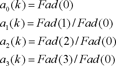
この場合、他のADC10の周波数特性をADC10-0の周波数特性で除算したものを、当該他のADC10の周波数特性al(k)とすることにより、補正を行うことができる。すなわち、予め測定したADC10-l(l=0、1、2、3)の周波数特性をそれぞれFad(l)とすると、補正に用いるそれぞれの周波数特性al(k)は下式で表される。
・・・式(11)
また、式(11)に示した周波数特性を用いて、式(9)及び式(10)は以下のように表される。

・・・式(9)

・・・式(10)
以上については、与えられるアナログ信号を複素信号として説明したが、与えられるアナログ信号が実信号である場合には、上述した補正方法のうち、第1領域及び第2領域に対応する動作のみを適用する。例えば合成段階S208では、第1領域及び第2領域における周波数スペクトルを、式(6)又は式(7)に基づいて算出される補正係数を式(9)に用いることにより算出し、第1領域及び第2領域における周波数スペクトルの複素共役を第3領域及び第4領域における周波数スペクトルとして算出する。
また、本例においては算出する周波数スペクトルの帯域を[0、4fs]として説明したが、当該帯域を[-2fs、2fs]としても同様の動作を行うことができる。例えば、第3領域の帯域を[-fs、0]、第4領域の帯域を[-2fs、-fs]とすることにより、同様の動作でスプリアス成分を除去することができる。
また、それぞれの周波数特性は、k=0の周波数特性a(0)を基に、以下のように算出してもよい。
a(-1)・・・a(0)を-fs/4シフト
a(1)・・・a(0)をfs/4シフト
a(2)・・・a(0)を2fs/4シフト
a(3)・・・a(0)を3fs/4シフト
a(5)・・・a(0)を5fs/4シフト
a(-1)・・・a(0)を-fs/4シフト
a(1)・・・a(0)をfs/4シフト
a(2)・・・a(0)を2fs/4シフト
a(3)・・・a(0)を3fs/4シフト
a(5)・・・a(0)を5fs/4シフト
また、フーリエ変換部12が離散フーリエ変換によってフーリエ変換を行う場合、式(1)に示したサンプリングクロックの離散フーリエ変換は下式で与えられる。
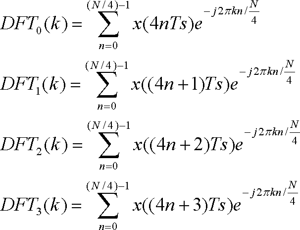
・・・式(11)
そして、離散フーリエ変換された測定信号は下式で与えられる。

このため、式(9)及び式(10)は以下のように表される。

・・・式(9)'

・・・式(10)'
また、本例においてはADC10の個数を4として説明したが、ADC10の個数がN(但しNは2以上の整数)であっても、同様にスプリアス成分を除去した周波数スペクトルを算出することができる。例えば、式(4)、式(5)、式(9)、及び式(10)は下式にように表される。

(但し上式において、-lからmまでの項は、X(f)の帯域を[-Nfs/2、Nfs/2](但しfsは、それぞれのアナログデジタルコンバータのサンプリング周波数)とした場合に、帯域[0、Nfs]に含まれる成分であり、aj(k)は、j番目のアナログデジタルコンバータの周波数特性のうちの、


(但し上式において、α、βは任意の実数、x(u)はx(0)のエイリアシング成分)


また、複数のADC10によって、nポイントのサンプリングデータを取得した場合、それぞれのフーリエ変換部12には、n/Nポイントのデータが入力される(ただし、NはADC10の個数。以下ではN=4として説明する)。このため、フーリエ変換部12は、4個のADC10全体によるサンプリング周波数をfとすると、0からf/4の帯域の周波数領域信号を出力する。これに対し、インターリーブ部18は、0からfの帯域の周波数領域信号を出力する。このため、補正部16において、上述した帯域の差を補償して補正を行うことが好ましい。
図8Aは、補正部16における帯域補償の一例を示す図である。なお、図8A、B、Cでは、信号成分およびそのイメージ成分を実線で示し、これらの複素共役成分を破線で示す。上述したように、それぞれの補正部16には、0からf/4の帯域の周波数領域信号が入力される。また、f/2から3f/4の帯域にはイメージ成分があらわれる。補正部16は、当該周波数領域信号およびイメージ成分について複素共役成分を生成する。そして、補正部16は、それぞれの複素共役成分を、f/4および3f/4を境界として、信号成分と鏡像となるようにコピーする。これにより、0からfの帯域の周波数領域信号を生成することができる。
補正部16は、帯域を補償した周波数領域信号に対して、図1から図7に関連して説明した補正を行ってよい。補正部16が補正した周波数領域信号を、インターリーブ部18で合成することで、0からfの帯域の信号を生成することができる。
図8Bは、補正部16における帯域補償の他の例を示す図である。本例の補正部16は、図8Bに示すように、0からf/4の帯域の周波数領域信号について、複素共役成分を生成する。そして、補正部16は、それぞれの複素共役成分を、f/4を境界として信号成分と鏡像になるようにコピーする。これにより、0からf/2の帯域の周波数領域信号を生成することができる。補正部16は、帯域を補償した周波数領域信号に対して、図1から図7に関連して説明した補正を行ってよい。図8Bに示した例では、インターリーブ部18において更に帯域を補償する。
図8Cは、図8Bに関連して説明した補正部16における帯域補償のあとの、インターリーブ部18における帯域補償の例を示す図である。上述したように、それぞれの補正部16は、0からf/2の帯域の周波数領域信号を出力する。インターリーブ部18は、これらの周波数領域信号を合成して、0からf/2の帯域の合成信号を生成する。そして、インターリーブ部18は、合成信号の複素共役成分を、f/2を境界として信号成分と鏡像になるようにコピーする。これにより、0からfの帯域の合成信号を生成することができる。
図9は、インターリーブAD変換装置100の構成の他の例を示す図である。本例のインターリーブAD変換装置100は、複数のADC(10-0~10-7)、複数のフーリエ変換部(12-0~12-7)、複数のグループ内補正部(20-0~20-1)、グループ間補正部30、および、測定部14を備える。ADC10、フーリエ変換部12、および、測定部14は、図1に関連して説明したADC10、フーリエ変換部12、および、測定部14と同一の機能を有する。
グループ内補正部20は、複数の測定信号を複数のグループに分割したグループ毎に設けられる。それぞれのグループ内補正部20は、対応する測定信号のグループに対して、図1から図7に関連して説明した補正を行う。つまり、それぞれのグループ内補正部20は、所属するグループ内の全てのADC10の周波数特性に基づく補正係数を、それぞれの測定信号に乗ずることにより、対応するADC10の周波数特性が理想的である場合に得られる測定信号に変換する。それぞれのグループ内補正部20は、対応するADC10の周波数特性を、測定部14から受け取ってよい。
より具体的には、それぞれのグループ内補正部20は、対応するグループについて、式(5)から式(8)に関連して説明した第1補正係数Lを算出する。また、それぞれのグループ内補正部20は、対応するグループについて、式(9)および式(10)に関連して説明した第2補正係数を算出する。そして、それぞれのグループ内補正部20は、対応するグループについて、第1補正係数および第2補正係数を用いて、式(9)および式(10)に関連して説明した補正を行う。また、グループ内補正部20は、補正した複数の測定信号を、式(9)および式(10)に関連して説明したように合成して出力してよい。
このように、それぞれのグループ内補正部20において、図1から図7に関連して説明した補正を行うので、複数の測定信号は、それぞれが2のべき乗個の測定信号を含むグループに分割されることが好ましい。また、複数の測定信号は、それぞれが同一個数の測定信号を含むグループに分割されることが好ましい。
また、複数の測定信号は、複数の測定信号間の相対位相差がグループ内で均一となり、且つ、グループ間で等しくなるように分割されることが好ましい。本例では、複数の測定信号は、ADC10-0、10-4、10-2、10-6に対応するグループと、ADC10-1、ADC10-5、ADC10-3、ADC12-7に対応するグループとに分割される。
なお、ADC10-0~ADC10-7は、図2に示した例と同様に、位相が所定値ずつずれたサンプリングクロックが与えられる。例えば、サンプリングクロックの周期を8Tsとすると、ADC10-mには、ADC10-0のサンプリングクロックに対してm×Tsだけ位相が遅れたサンプリングクロックが与えられる。上述したようにグループを分割することで、各グループに4個(つまり、同一且つ2のべき乗個)の測定信号が属することになる。また、グループ内における測定信号間の相対位相差が2Tsで均一となり、また、当該相対位相差2Tsは、グループ間で同一となる。
また、それぞれのグループ内補正部20は、対応するグループに含まれる複数のADC10のうち、いずれか一のADC10の周波数特性を基準として、当該グループにおける測定信号を補正してよい。本例では、グループ内補正部20-0は、ADC10-0に対応する測定信号を基準とし、グループ内補正部20-1は、ADC10-1に対応する測定信号を基準とする。
グループ間補正部30は、それぞれのグループ内補正部20が補正したそれぞれのグループ間の周波数特性差に基づいて、それぞれのグループの周波数特性を補正して合成し、デジタル信号の周波数スペクトルを生成する。グループ間補正部30は、いずれかのグループの周波数特性を基準として、各グループの周波数特性を補正してよい。
例えば、グループ間補正部30は、グループ内補正部20-0のグループの周波数特性を基準として、各グループの周波数特性を補正してよい。本例では、グループ内補正部20-0のグループは、ADC10-0の周波数特性にあわせてあり、グループ内補正部20-1のグループは、ADC10-1の周波数特性にあわせてある。このため、グループ間補正部30は、ADC10-0およびADC10-1の周波数特性に基づいて、各グループの測定信号を補正してよい。グループ間補正部30には、それぞれのグループ内補正部20において基準とされたADC10の周波数特性が、測定部14から与えられてよい。
グループ間補正部30は、グループ内補正部20が出力する信号を1つの測定信号として、各グループ内補正部20が出力する信号を、図1から図7に関連して説明した方法で補正してよい。このような構成によっても、複数のADC10の周波数特性差を補償した信号を生成することができる。また、図1から図7に関連して説明した方法では、第1補正係数および第2補正係数を算出するのに、N-1次元の行列演算をしなければならない(ただしNは、ADC10の個数)。これに対し、本例のインターリーブAD変換装置100では、グループ内補正部20においては(N/k)-1次元の行列演算を行い(ただしkは分割数)、グループ間補正部30ではk-1次元の行列演算を行えばよい。このため、行列演算の次数を低減することができ、簡易な計算で補正係数を算出することができる。
図10は、図9に示したインターリーブAD変換装置100の動作の一例を示すフローチャートである。本例のインターリーブAD変換装置100は、まず、図7に関連して説明したS200からS204の動作を行う。
そして、グループ内補正段階S210において、グループ内補正部20は、それぞれのグループに含まれる測定信号を補正する。S210では、それぞれのグループにおいて、図7に関連して説明したS206およびS208の処理を行ってよい。
そして、グループ間補正段階212において、グループ間補正部30は、それぞれのグループ間の周波数特性差に基づいて測定信号を補正する。S212では、それぞれのグループ内補正部20の出力を1つの測定信号として、S206およびS208の処理を行ってよい。このような動作により、簡易な処理で周波数特性差を補償することができる。
図11は、インターリーブAD変換装置100の構成の他の例を示す図である。本例のインターリーブAD変換装置100は、複数の補正ステージを有し、各補正ステージにおいて2チャネル毎に周波数特性差を補正する。この場合、グループ内補正部20が初段の補正ステージとして機能し、グループ間補正部30が次段以降の補正ステージとして機能してよい。
本例のインターリーブAD変換装置100は、2つのADC10ごとに、1つのグループ内補正部20を備える。このため、グループ内補正部20は、複数の測定信号を、2つの測定信号毎のグループに分割して周波数特性差を補正する。
本例においても、それぞれのグループ内補正部20には、対応するADC10のペアの相対位相差が、他のペアと同一となるように、それぞれのADC10を対応付ける。例えば、それぞれのADC10のペアの相対位相差(本例では4Ts)が、サンプリングクロックの周期(本例では8Ts)の略半分となるように、ADC10をペアリングする。
より具体的には、ADC10のペアリングは、整数を2進数表記し、ビットの並びを左右反転させた結果に基づいて定めてよい。例えば整数0および1を2進数表記したものは、000および001となる。これをビットリバースさせると、000および100となる。当該2進数は、整数0および4を示すので、グループ内補正部20-0には、ADC10-0およびADC10-4のペアを対応させる。
同様に、整数2および3を2進数表記したものは、010および011となる。これをビットリバースさせると、010および110となる。当該2進数は、整数2および6を示すので、グループ内補正部20-2には、ADC10-2およびADC10-6を対応させる。同様に、グループ内補正部20-1には、ADC10-1およびADC10-5を対応させ、グループ内補正部20-3には、ADC10-3およびADC10-7を対応させる。
それぞれのグループ内補正部20は、いずれかの測定信号に対応するADC10の周波数特性を基準として、各測定信号を補正してよい。それぞれのグループ内補正部20には、測定部14から、対応するADC10の周波数特性が与えられる。グループ内補正部20における処理は、図1から図7に関連して説明した処理において、ADC10の個数を2とした場合と同一でよい。
グループ間補正部30は、それぞれのグループ内補正部20が出力するグループを、対応するグループのペアに分け、それぞれのグループのペアにおける周波数特性差に基づいて、それぞれのグループのペアの周波数特性を補正し、当該2つのグループを合成した新たなグループを生成する。そして、グループ間補正部30は、グループが1つに合成されるまで、グループの合成を繰り返す。
グループ間補正部30は、複数段階の補正部を有する。本例のグループ間補正部30は、2段階に設けられた複数の第1補正部32および第2補正部34を有する。それぞれの第1補正部32は、対応する2つのグループ内補正部20の出力を受け取り、対応するADC10の周波数特性差に基づいて補正する。例えば、第1補正部32-0は、グループ内補正部20-0で基準とされたADC10-0およびグループ内補正部20-2で基準とされたADC10-2の周波数特性に基づいて、それぞれのグループ内補正部20が出力した信号を補正する。第1補正部32における処理は、図1から図7に関連して説明した処理において、ADC10の個数を2とした場合と同一でよい。それぞれの第1補正部32に、いずれのグループ内補正部20を対応付けるかは、ADC10のペアリングと同様の条件で決定してよい。
また、第2補正部34は、2つの第1補正部32の出力を受け取り、対応するADC10の周波数特性差に基づいて補正する。第2補正部34における処理は、図1から図7に関連して説明した処理において、ADC10の個数を2とした場合と同一でよい。
このような構成により、各補正部における行列演算を、1次元の行列演算とすることができる。このため、簡易な処理で周波数特性差を補償することができる。また、各補正部の処理が同様になるので、同一構成の補正部を設計すればよい。この場合、各補正部で用いる補正係数をそれぞれ独立に設定する。
また、図1から図7においては、周波数領域をADC10の個数に応じて分割して補正係数を算出した。本例でも、各補正部に2チャネルの信号が入力されるので、本来は各補正部において、周波数領域を2分割して補正係数を算出することになる。しかし、周波数領域を2分割した場合、各領域の境界がナイキスト周波数となるので、分割された各領域は、複素共役の関係になる。つまり、各領域について、式(5)から式(10)に従って算出される補正係数は同一となる。このため、本例のインターリーブAD変換装置100は、それぞれの補正部に対して、周波数領域を分割せずに補正係数を算出してよい。または、分割した一方の周波数領域に対して算出した補正係数を、他方の周波数領域においても用いてよい。このため、更に簡易な処理で周波数特性差を補償することができる。
図12は、図11に示したインターリーブAD変換装置100の動作の一例を示すフローチャートである。本例のインターリーブAD変換装置100は、まず、図7に関連して説明したS200からS204の動作を行う。
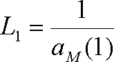
そして、最初の補正段階S214において、グループ内補正部20は、ペアリングされた2つの測定信号ごとに、対応するADC10の周波数特性に基づいて補正して合成する。補正段階S214では、それぞれのペアについて、それぞれのADC10の周波数特性により生じる、それぞれの測定信号のスプリアス成分がうち消し合うように、いずれか一方の測定信号に乗ずる第1補正係数を、2つのADC10の周波数特性に基づいて算出する。具体的には、下式に基づいて第1補正係数L1を算出してよい。

・・・式(11)
ただし、aM(1)は、第1補正係数が乗じられる測定信号に対応するADC10の周波数特性のうちの、スプリアス成分に対応する成分を示す。なお、第1補正係数が乗じられる測定信号に対応するADC10の周波数特性aM(k)は、基準となるADC10の周波数特性aR(k)を基準とする(つまり、aR(k)=1として正規化された周波数特性を用いる)。
ただし、aM(1)は、第1補正係数が乗じられる測定信号に対応するADC10の周波数特性のうちの、スプリアス成分に対応する成分を示す。なお、第1補正係数が乗じられる測定信号に対応するADC10の周波数特性aM(k)は、基準となるADC10の周波数特性aR(k)を基準とする(つまり、aR(k)=1として正規化された周波数特性を用いる)。
例えば、図11に示した例では、グループ内補正部20-0は、a0(k)=1とした周波数特性a4(1)を用いて、第1補正係数L1を算出する。同様に、グループ内補正部20-2は、a2(k)=1とした周波数特性a6(1)を用いて、第1補正係数L1を算出する。同様に、グループ内補正部20-1は、a1(k)=1とした周波数特性a5(1)を用いて、第1補正係数L1を算出する。同様に、グループ内補正部20-4は、a4(k)=1とした周波数特性a7(1)を用いて、第1補正係数L1を算出する。
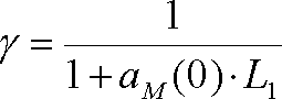
また、補正段階S214では、それぞれのペアについて、第1補正係数を乗じたことにより生じる、測定信号の信号成分の位相の誤差を補正する第2補正係数γを、第1補正係数L1及びそれぞれのADC10の周波数特性に基づいて算出する。具体的には、下式に基づいて補正係数γを算出してよい。

・・・式(12)
ただし、aM(0)は、第1補正係数L1が乗じられる測定信号に対応するADC10の周波数特性のうちの、信号成分に対応する成分を示す。
ただし、aM(0)は、第1補正係数L1が乗じられる測定信号に対応するADC10の周波数特性のうちの、信号成分に対応する成分を示す。
例えば、図11に示した例では、グループ内補正部20-0は、a0(k)=1とした周波数特性a4(0)を用いて、第2補正係数γを算出する。同様に、グループ内補正部20-2は、a2(k)=1とした周波数特性a6(0)を用いて、第2補正係数γを算出する。同様に、グループ内補正部20-1は、a1(k)=1とした周波数特性a5(0)を用いて、第2補正係数γを算出する。同様に、グループ内補正部20-4は、a4(k)=1とした周波数特性a7(0)を用いて、第2補正係数γを算出する。
そして、補正段階214では、それぞれのグループについて、第1補正係数L1及び第2補正係数γに基づいて、それぞれの測定信号を補正して合成する。具体的には、下式に基づいて信号を補正および合成してよい。

・・・式(13)
ただし、DFTR(k)は、補正部に入力される2つの測定信号のうち、基準となる測定信号を示す。また、DFTM(k)は、補正部に入力される2つの測定信号のうち、基準でない測定信号を示す。
ただし、DFTR(k)は、補正部に入力される2つの測定信号のうち、基準となる測定信号を示す。また、DFTM(k)は、補正部に入力される2つの測定信号のうち、基準でない測定信号を示す。
補正段階214により、各グループで信号を合成した結果、全ての測定信号が1つのグループに合成されていれば、処理を終了する(S216)。まだ測定信号が複数のグループに分割されている場合、グループが1つになるまで補正段階S214を繰り返す。2回目以降の補正段階S214は、グループ間補正部30が行ってよい。このとき、それぞれの第1補正部32には、式(13)で示される信号が2つ与えられる。そして、これらの信号を、式(11)、式(12)、および、式(13)を用いて補正および合成する。
例えば、第1補正部32-0は、周波数特性a0(k)を基準とした周波数特性a4(k)をaM(k)として、式(11)および式(12)に基づいて補正係数を算出し、式(13)に基づいて信号を合成してよい。同様に、第1補正部32-1は、周波数特性a1(k)を基準とした周波数特性a3(k)をaM(k)として、式(11)および式(12)に基づいて補正係数を算出し、式(13)に基づいて信号を合成してよい。
また、第2補正部34は、第1補正部32-0および第1補正部32-1がそれぞれ出力する信号を受け取る。第2補正部34は、これらの信号を、式(11)、式(12)、および、式(13)を用いて補正および合成する。例えば、第2補正部34は、周波数特性a0(k)を基準とした周波数特性a1(k)をaM(k)として、式(11)および式(12)に基づいて補正係数を算出し、式(13)に基づいて信号を合成してよい。このように、複数段階の補正部により2チャネルごとに補正および合成を行う例ので、同様の処理を繰り返すことで、多数のチャネルの信号の補正および合成を容易に行うことができる。
なお、図8Aから図8Cに関連して説明したように、各補正ステージにおいて補正および合成の処理を行うと、次段の補正ステージで取り扱うサンプリングデータの数は2倍となる。例えば、最終段の補正ステージでnポイントのサンプリングデータを取り扱う場合、その前段の補正ステージではn/2ポイントのサンプリングデータを取り扱う。
このため、各補正ステージにおける補正部は、合成した周波数領域信号について、周波数軸における複素共役成分を、各補正ステージのナイキスト周波数に対して鏡像に複製してよい。例えば、最終段の補正ステージでは、合成した周波数領域信号の複素共役成分を、周波数N×fs/2に対して鏡像に複製してよい。また、その前段の補正ステージでは、合成した周波数領域信号の複素共役成分を、周波数N×fs/4に対して鏡像に複製してよい。ただし、NはADC10の個数、fsは、それぞれのADC10のサンプリング周波数を示す。なお、それぞれの補正部では、複素共役成分を複製した信号に対して、第2補正係数を乗算してよい。
また、以上の例においては、各補正部において第2補正係数を乗算したが、他の例では、最終段の補正ステージにおける補正部において、全段の補正ステージにおける第2補正係数を合成した第2補正係数を乗算してもよい。この場合、最終段の補正ステージにおける第2補正係数は、式(9)'で示したように、1/(1+Σak(0)・Lk)で与えられてよい(ただし、kは各ADC10の番号)。
図13は、インターリーブAD変換装置100の構成の他の例を示す図である。本例のインターリーブAD変換装置100は、図11に示したインターリーブAD変換装置100の構成に対して、グループ内補正部20およびグループ間補正部30に代えて、複数の補正部22を有する。複数の補正部22は、図11に関連して説明したグループ内補正部20と同一の機能を有してよい。また、補正部22は、2つのADC10ごとに、1つずつ設けられる。上述したように、2回目以降の補正段階S214においても、補正係数を変更して、最初の補正段階S214と同一の処理が行われる。このため、本例のインターリーブAD変換装置100は、それぞれの補正段階S214で補正部22を共用する。
補正部22は、図12に示した補正段階S214において、2チャネルの信号ペア毎に補正および合成を行う。例えば最初の補正段階S214では、補正部22は、対応するフーリエ変換部12が出力する測定信号に対して、補正および合成を行う。このときの補正部22の動作は、図11に関連して説明したグループ内補正部20と同一であってよい。
2回目の補正段階S214では、最初の補正段階S214において補正部22が生成した合成信号を、補正部22に入力する。本例では、補正部22-0および補正部22-1に、補正部22-2および補正部22-3が合成した信号が入力される。
補正部22-0は、最初の補正段階S214において自己が生成した合成信号と、補正部22-2が生成した合成信号とを、補正および合成する。また、補正部22-1は、最初の補正段階S214において自己が生成した合成信号と、補正部22-3が生成した合成信号とを、補正および合成する。
3回目の補正段階S214では、補正部22-0に、補正部22-1が2回目の補正段階において生成した合成信号を入力する。補正部22-0は、2回目の補正段階S214において自己が生成した合成信号と、補正部22-1が生成した合成信号とを、補正および合成する。このような構成により、小規模のハードウェアを用いて、且つ、簡易な処理により多数のチャネルの測定信号を補正および合成することができる。
図14は、インターリーブAD変換装置100の他の構成例を示す図である。図9から図13に関連して説明したインターリーブAD変換装置100のグループ内補正部20およびグループ間補正部30は、フーリエ変換部12においてフーリエ変換された測定信号に対して周波数領域で補正を行った。これに対し、本例のインターリーブAD変換装置100のグループ内補正部20およびグループ間補正部30は、対応するADC10の周波数特性に応じたフィルタ係数を有するデジタルフィルタを用いて、時間領域のそれぞれの測定信号を補正する。
本例のインターリーブAD変換装置100は、図9から図13に関連して説明したインターリーブAD変換装置100の構成に対して、複数のフーリエ変換部12に代えて、複数のデータ挿入部28およびデータ挿入部29を備える。
複数のデータ挿入部28は、複数のADC10と対応して設けられ、それぞれ対応するADC10が出力する測定信号の各データ間に、データ値0のデータを予め定められた個数挿入する。また、複数のデータ挿入部29は、複数のグループ内補正部20に対応して設けられ、それぞれ対応するグループ内補正部20が出力する合成信号の各データ間に、データ値0のデータを予め定められた個数挿入する。例えば、それぞれのデータ挿入部28およびデータ挿入部29は、図15に示すように、測定信号のデータの各データ間に、データ値0のデータを、N-1個ずつ挿入する。データ挿入部28は、挿入後の測定信号の各データ間隔が略等しくなるように、データ値0のデータを挿入することが好ましい。
なお、Nは後段の補正部に入力される信号の本数を示す。本例では、データ挿入部28は、後段の補正部に4本ずつ信号が入力されるので、各測定信号のデータ間に3個ずつ0を挿入する。また、データ挿入部29は、後段の補正部に2本の信号が入力されるので、各測定信号のデータ間に1個ずつ0を挿入する。
また、本例のグループ内補正部20およびグループ間補正部30は、フィルタ部24、合成部25、および、フィルタ部26を有する。それぞれのフィルタ部におけるフィルタ係数を設定することで、上述したグループ内補正部20およびグループ間補正部30の補正処理を時間領域で行う。
フィルタ部24は、それぞれの補正部に入力されるそれぞれの測定信号に対して設けられる。ただし、図14に示すように、基準となる入力に対しては、フィルタ部24が設けられなくともよい。それぞれのフィルタ部24は、対応するADC10の周波数特性に応じたフィルタ係数が設定され、対応する測定信号を通過させて合成部25に供給する。具体的には、それぞれのフィルタ部24は、対応する第1補正係数Lをフーリエ逆変換したフィルタ係数を有する。
合成部25は、フィルタ部24を介してそれぞれの測定信号を受け取り、受け取った測定信号を合成する。ここで、合成とは各測定信号のデータにおいて、同位相のデータを加算することをいう。
フィルタ部26は、対応するADC10の周波数特性に応じたフィルタ係数が設定され、合成部25が合成した測定信号を通過させる。フィルタ部26は、式(9)および式(10)に関連して説明した第2補正係数(1/Σak(0)×Lk)をフーリエ逆変換したフィルタ係数を有してよい。また、測定部14は、各ADC10の周波数特性に基づいて、各フィルタ部のフィルタ係数を制御してよい。
すなわち、それぞれのフィルタ部24は、それぞれの測定データを周波数領域の信号に変換して合成した場合に、複数のADC10の周波数特性により生じるスプリアス成分が打ち消し合うような第1の補正係数(例えばLk、ただしkは当該フィルタ部24に対応するADC10の番号)をフーリエ逆変換したフィルタ係数を有する。また、フィルタ部26は、第1補正係数を乗算することにより生じる位相誤差を補正するための第2の補正係数(例えば、1/Σak(0)×Lk、ただし、kは当該グループに属するADC10の番号)をフーリエ逆変換したフィルタ係数を有する。ここで、第1の補正係数は、式(6)から式(8)に示したように、デジタル信号の周波数帯域を分割した分割帯域毎に定まる係数であってよい。また、第2の補正係数も、式(9)及び式(10)に示したように、分割帯域毎に定まる係数であってよい。これにより、ADC10の周波数特性の誤差により生じるスプリアス成分を除去したデジタル信号を生成することができる。
なお図14の例では、各補正ステージにフィルタ部26を設ける例を説明した。他の例では、最終段の補正ステージにのみフィルタ部26を設けてよい。この場合、最終段の補正ステージのフィルタ部26は、各段の補正ステージにおいてフィルタ部26が有するべきフィルタ係数を合成したフィルタ係数を有してよい。例えば、最終段の補正ステージのフィルタ部26は、1/(1+Σak(0)・Lk)をフーリエ逆変換したフィルタ係数を有してよい(ただし、kはインターリーブAD変換装置100が備えるADC10の番号)。
図15は、データ挿入部の動作を説明する図である。上述したように、データ挿入部28は、対応するADC10が出力する測定信号の各データ間に、データ値ゼロのデータを所定の個数挿入する。例えば、ADC10-0は、{D0、D4、D8、・・・}と測定信号を出力するが、データ挿入部28-0は、測定信号の各データ間にデータ値ゼロのデータを3個ずつ挿入してよい。これにより、データ挿入部28-0が出力する測定信号のデータ列は、{D0、0、0、0、D4、0、0、0、D8、0、0、0、・・・}となる。
また、各ADC10が出力する測定信号のデータの位相は、図15に示すようにTsずつ異なる。データ挿入部28は、それぞれの測定信号の各データ間に、データ値0のデータを所定位相Ts毎に挿入することが好ましい。
なお、図11から図13に関連して説明したように、2チャネル毎に補正処理を行う例においても、図14および図15に関連して説明した構成と同様に、それぞれの補正処理を、デジタルフィルタを用いて時間領域で行ってよい。この場合、データ挿入部は、各補正部の各入力に対して設けられる。それぞれのデータ挿入部は、各補正部に入力されるそれぞれの入力信号に対して、各データ間に1つずつ0を挿入してよい。
また、図13に示した例では、それぞれの補正部22の内部に、入力された2つの信号にそれぞれデータを挿入するデータ挿入部が設けられてよい。このような構成により、各補正ステージの処理で、補正部22を共用することができる。
図16は、インターリーブAD変換装置100の他の構成例を示す図である。本例のインターリーブAD変換装置100は、図13に関連して説明したインターリーブAD変換装置100の構成に対して、それぞれの補正部においてフィルタ部24-0を更に有する。また、最終段以外の補正ステージにおいては、フィルタ部26を有さない。例えば、図16に示すように、2段の補正ステージを有する構成では、1段目のグループ内補正部20は、フィルタ部26に代えてフィルタ部24-0を有する。また、2段目のグループ間補正部30は、図13に関連して説明した構成に対して、フィルタ部24-0を追加した構成であってよい。
それぞれのフィルタ部24-0は、各補正部において基準となるADC10に対応するパスに設けられる。フィルタ部24-0は、補正部ごとに算出される第2補正係数を用いて、基準となる測定信号を補正する。また、他のフィルタ部24-1、2、3、・・・は、補正部ごとに算出される第1補正係数および第2補正係数を用いて、対応する測定信号を補正する。
また最終段の補正部におけるフィルタ部26は、1/a0(0)をフーリエ逆変換したフィルタ係数が設定され、合成部25が出力する信号を通過させる。このような構成によっても、式(9)および式(10)に関連して説明した補正処理を行うことができる。
以上から明らかなように、インターリーブAD変換装置100によれば、インターリーブAD変換において、スプリアス成分を除去した周波数スペクトルを得ることができる。また、測定信号を分割して処理することにより、簡易な処理でスプリアス成分を除去した周波数スペクトルを得ることができる。
以上、本発明を実施の形態を用いて説明したが、本発明の技術的範囲は上記実施の形態に記載の範囲には限定されない。上記実施の形態に、多様な変更または改良を加えることが可能であることが当業者に明らかである。その様な変更または改良を加えた形態も本発明の技術的範囲に含まれ得ることが、請求の範囲の記載から明らかである。
請求の範囲、明細書、および図面中において示した装置、システム、プログラム、および方法における動作、手順、ステップ、および段階等の各処理の実行順序は、特段「より前に」、「先立って」等と明示しておらず、また、前の処理の出力を後の処理で用いるのでない限り、任意の順序で実現しうることに留意すべきである。請求の範囲、明細書、および図面中の動作フローに関して、便宜上「まず、」、「次に、」等を用いて説明したとしても、この順で実施することが必須であることを意味するものではない。
10・・ADC、12・・・フーリエ変換部、14・・・測定部、16・・・補正部、18・・・インターリーブ部、20・・・グループ内補正部、22・・・補正部、24、26・・・フィルタ部、25・・・合成部、28、29・・・データ挿入部、30・・・グループ間補正部、32・・・第1補正部、34・・・第2補正部、100・・・インターリーブAD変換装置
Claims (22)
- アナログ信号を、与えられるサンプリングクロックの位相がそれぞれ所定の周期ずつ異なる複数のアナログデジタルコンバータを用いてデジタル信号に変換するアナログデジタル変換方法であって、
前記複数のアナログデジタルコンバータにおけるそれぞれのアナログデジタルコンバータの周波数特性を予め測定する測定段階と、
前記複数のアナログデジタルコンバータを用いて、前記アナログ信号をサンプリングするサンプリング段階と、
前記複数のアナログデジタルコンバータを用いて生成した複数の測定信号を複数のグループに分割したグループ毎に、前記複数の測定信号におけるそれぞれの測定信号に対して、所属するグループ内の全ての前記アナログデジタルコンバータの前記周波数特性に基づく補正係数を乗ずることにより、対応する前記アナログデジタルコンバータの前記周波数特性が理想的である場合に得られる測定信号に変換するグループ内補正段階と、
前記グループ内補正段階により得られたそれぞれの前記グループ間の周波数特性差に基づいて、それぞれの前記グループの周波数特性を補正して合成し、前記デジタル信号の周波数スペクトルを生成するグループ間補正段階と
を備えるアナログデジタル変換方法。 - 前記グループ内補正段階において、それぞれの前記グループに含まれる前記複数のアナログデジタルコンバータ毎に、いずれか一の前記アナログデジタルコンバータの前記周波数特性を基準として、当該グループにおける前記測定信号の前記周波数特性を補正する請求項1に記載のアナログデジタル変換方法。
- 前記グループ間補正段階において、いずれかの前記グループの周波数特性を基準として、他の前記グループの周波数特性を補正する
請求項2に記載のアナログデジタル変換方法。 - 前記グループ内補正段階において、前記複数の測定信号を、それぞれが同一個数の前記測定信号を含む前記グループに分割する
請求項3に記載のアナログデジタル変換方法。 - 前記グループ内補正段階において、前記複数の測定信号を、それぞれが2のべき乗個の前記測定信号を含む前記グループに分割する
請求項4に記載のアナログデジタル変換方法。 - 前記グループ内補正段階において、前記複数の測定信号を、2つの前記測定信号毎の前記グループに分割して前記周波数特性を補正し、
前記グループ間補正段階は、
前記複数のグループを、対応する前記グループのペアに分け、それぞれの前記グループのペアにおける周波数特性差に基づいて、それぞれの前記グループのペアの周波数特性を補正し、当該2つの前記グループを合成した新たなグループを生成するペア合成段階と、
前記グループが1つになるまで、前記ペア合成段階を繰り返す繰返段階と
を有する請求項3に記載のアナログデジタル変換方法。 - 前記グループ内補正段階は、
それぞれの前記グループについて、それぞれの前記アナログデジタルコンバータの前記周波数特性により生じる、それぞれの前記測定信号のスプリアス成分がうち消し合うように、いずれか一方の前記測定信号に乗ずる第1補正係数を、2つの前記アナログデジタルコンバータの前記周波数特性に基づいて算出する第1算出段階と、
それぞれの前記グループについて、前記第1補正係数を乗じたことにより生じる、前記測定信号の信号成分の誤差を補正する第2補正係数を、前記第1補正係数及びそれぞれの前記アナログデジタルコンバータの前記周波数特性に基づいて算出する第2算出段階と、
それぞれの前記グループについて、前記第1補正係数及び前記第2補正係数に基づいて、それぞれの前記測定信号を補正する係数乗算段階と
を有する請求項6に記載のアナログデジタル変換方法。 - 前記第1算出段階において、下式に基づく第1補正係数L1を算出し、
前記第2算出段階において、下式に基づく第2補正係数γを算出する
請求項7に記載のアナログデジタル変換方法。 - 前記複数のアナログデジタルコンバータが出力する前記測定信号をそれぞれフーリエ変換するフーリエ変換段階を更に備え、
前記グループ内補正段階および前記グループ間補正段階において、前記フーリエ変換段階においてフーリエ変換された前記測定信号に対して、周波数領域で補正を行う
請求項3に記載のアナログデジタル変換方法。 - 前記グループ内補正段階および前記グループ間補正段階において、対応する前記アナログデジタルコンバータの周波数特性に応じたフィルタ係数を有するデジタルフィルタを用いて、時間領域のそれぞれの前記測定信号を補正する
請求項3に記載のアナログデジタル変換方法。 - 前記グループ内補正段階は、
それぞれの前記グループについて、それぞれの前記アナログデジタルコンバータの前記周波数特性により生じる、それぞれの前記測定信号のスプリアス成分がうち消し合うように、それぞれの前記測定信号に乗ずるそれぞれの第1補正係数を、全ての前記アナログデジタルコンバータの前記周波数特性に基づいて算出する第1算出段階と、
それぞれの前記グループについて、前記第1補正係数を乗じたことにより生じる、前記測定信号の信号成分の位相の誤差を補正する第2補正係数を、それぞれの前記第1補正係数及びそれぞれの前記周波数特性に基づいて算出する第2算出段階と
を有し、
それぞれの前記測定信号に、対応する前記第1補正係数を乗じ、
前記補正段階において対応する前記第1補正係数が乗算されたそれぞれの測定信号を合成し、合成した信号に前記第2補正係数を乗ずる
請求項1に記載のアナログデジタル変換方法。 - 前記グループ内補正段階は、
それぞれの前記グループについて、それぞれの前記アナログデジタルコンバータの前記周波数特性により生じる、それぞれの前記測定信号のスプリアス成分がうち消し合うように、それぞれの前記測定信号に乗ずるそれぞれの第1補正係数を、全ての前記アナログデジタルコンバータの前記周波数特性に基づいて算出する第1算出段階と、
それぞれの前記グループについて、前記第1補正係数を乗じたことにより生じる、前記測定信号の信号成分の位相の誤差を補正する第2補正係数を、それぞれの前記第1補正係数及びそれぞれの前記周波数特性に基づいて算出する第2算出段階と
を有し、
それぞれの前記測定信号に、対応する前記第1補正係数及び対応する前記第2補正係数を乗じる
請求項1に記載のアナログデジタル変換方法。 - 前記グループ内補正段階は、
それぞれの前記グループについて、算出するべき前記デジタル信号の周波数帯域を、前記アナログデジタルコンバータの個数に応じて分割し、
前記第1算出段階は、分割された前記周波数帯域毎に、それぞれの前記第1補正係数を算出し、
前記第2算出段階は、分割された前記周波数帯域毎に、前記第2補正係数を算出する
請求項11又は12に記載のアナログデジタル変換方法。 - 前記第1算出段階は、それぞれの前記測定信号の前記スプリアス成分のうち、分割されたそれぞれの前記周波数帯域に存在する前記スプリアス成分がうち消し合う前記第1補正係数を、分割されたそれぞれの前記周波数帯域毎に算出する請求項13に記載のアナログデジタル変換方法。
- 前記測定段階は、前記アナログ信号を前記デジタル信号に変換するときに与えられる前記サンプリングクロックを用いて、それぞれの前記周波数特性を測定することにより、与えられる前記サンプリングクロックの位相誤差を含んだそれぞれの前記周波数特性を測定する請求項1に記載のアナログデジタル変換方法。
- 前記グループ内補正段階は、それぞれがN個(但しNは2以上の整数)の前記測定信号を有する複数のグループを生成し、
それぞれの前記グループにおいて、N個の前記測定信号(X0(f)~XN-1(f))は下式で与えられ、
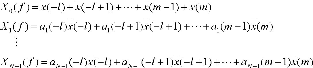

前記第1算出段階において、

を満たす前記第1補正係数(L1、L2、・・・LN-1)を算出する
請求項11又は12に記載のアナログデジタル変換方法。 - 前記第2算出段階において、下に示す前記第2補正係数を算出し、


- 前記グループ内補正段階は、それぞれがN個(但しNは2以上の整数)の前記測定信号を有する複数のグループを生成し、
それぞれの前記グループにおいて、それぞれの前記測定信号(X0(f)~X3(f))は下式で与えられ、


前記第1算出段階において、

を満たす前記第1補正係数(L1、L2、L3)を算出する
請求項11又は12に記載のアナログデジタル変換方法。 - 前記第2算出段階において、下に示す前記第2補正係数を算出し、


- 前記補正段階は、
算出するべき前記デジタル信号の周波数帯域を、帯域が[0、fs]である第1領域、帯域が[fs、2fs]である第2領域、帯域が[2fs、3fs]である第3領域、及び帯域が[3fs、4fs]である第4領域に分割し、
前記第1算出段階は、
前記第1領域における前記第1補正係数を下式に基づいて算出し、


- 前記グループ内補正段階は、
前記第1領域及び前記第2領域における前記合成信号の周波数スペクトルX'(f)を下式に基づいて算出し、


- アナログ信号を、デジタル信号に変換するアナログデジタル変換装置であって、
与えられるサンプリングクロックの位相がそれぞれ所定位相ずつ異なる複数のアナログデジタルコンバータと、
前記複数のアナログデジタルコンバータにおけるそれぞれのアナログデジタルコンバータの周波数特性を予め測定する測定部と、
前記複数のアナログデジタルコンバータが前記アナログ信号をサンプリングしたデータをそれぞれフーリエ変換し、前記複数のアナログデジタルコンバータに対応する複数の測定信号を生成するフーリエ変換部と、
前記複数の測定信号を複数のグループに分割したグループ毎に、前記複数の測定信号におけるそれぞれの測定信号に対して、所属するグループ内の全ての前記アナログデジタルコンバータの前記周波数特性に基づく補正係数を乗ずることにより、対応する前記アナログデジタルコンバータの前記周波数特性が理想的である場合に得られる理想測定信号に変換するグループ内補正部と、
前記グループ内補正部により得られたそれぞれの前記グループ間の周波数特性差に基づいて、それぞれの前記グループの周波数特性を補正するグループ間補正部と、
それぞれの前記理想測定信号を合成し、前記デジタル信号の周波数スペクトルを生成するインターリーブ部と
を備えるアナログデジタル変換装置。
Priority Applications (2)
| Application Number | Priority Date | Filing Date | Title |
|---|---|---|---|
| JP2010546463A JP5331823B2 (ja) | 2009-01-19 | 2009-12-07 | アナログデジタル変換方法、及びアナログデジタル変換装置 |
| US13/157,272 US8519872B2 (en) | 2009-01-19 | 2011-06-09 | Analog-digital converting method and analog-digital converting apparatus |
Applications Claiming Priority (2)
| Application Number | Priority Date | Filing Date | Title |
|---|---|---|---|
| JP2009-009247 | 2009-01-19 | ||
| JP2009009247 | 2009-01-19 |
Related Child Applications (1)
| Application Number | Title | Priority Date | Filing Date |
|---|---|---|---|
| US13/157,272 Continuation US8519872B2 (en) | 2009-01-19 | 2011-06-09 | Analog-digital converting method and analog-digital converting apparatus |
Publications (1)
| Publication Number | Publication Date |
|---|---|
| WO2010082268A1 true WO2010082268A1 (ja) | 2010-07-22 |
Family
ID=42339538
Family Applications (1)
| Application Number | Title | Priority Date | Filing Date |
|---|---|---|---|
| PCT/JP2009/006677 Ceased WO2010082268A1 (ja) | 2009-01-19 | 2009-12-07 | アナログデジタル変換方法、及びアナログデジタル変換装置 |
Country Status (3)
| Country | Link |
|---|---|
| US (1) | US8519872B2 (ja) |
| JP (1) | JP5331823B2 (ja) |
| WO (1) | WO2010082268A1 (ja) |
Families Citing this family (2)
| Publication number | Priority date | Publication date | Assignee | Title |
|---|---|---|---|---|
| US10135475B1 (en) * | 2017-10-11 | 2018-11-20 | The Boeing Company | Dynamic low-latency processing circuits using interleaving |
| CN117459064B (zh) * | 2023-12-25 | 2024-03-26 | 武汉市品持科技有限公司 | 多路adc采样方法、装置及设备 |
Citations (3)
| Publication number | Priority date | Publication date | Assignee | Title |
|---|---|---|---|---|
| JP2005347967A (ja) * | 2004-06-01 | 2005-12-15 | Advantest Corp | アナログディジタル変換方法、及びアナログディジタル変換装置 |
| WO2006126656A1 (ja) * | 2005-05-25 | 2006-11-30 | Advantest Corporation | アナログデジタル変換装置、プログラム、及び記録媒体 |
| WO2006126672A1 (ja) * | 2005-05-26 | 2006-11-30 | Advantest Corporation | アナログデジタル変換装置、プログラム、及び記録媒体 |
Family Cites Families (3)
| Publication number | Priority date | Publication date | Assignee | Title |
|---|---|---|---|---|
| GB2347289B (en) * | 1999-02-17 | 2001-01-10 | Advantest Corp | A high-speed waveform digitizer with a phase correcting means and a method therefor |
| JP4456720B2 (ja) | 1999-02-17 | 2010-04-28 | 株式会社アドバンテスト | インターリーブad変換方式波形デジタイザ装置 |
| JP2002246910A (ja) * | 2001-02-20 | 2002-08-30 | Advantest Corp | インターリーブad変換方式波形ディジタイザ装置 |
-
2009
- 2009-12-07 WO PCT/JP2009/006677 patent/WO2010082268A1/ja not_active Ceased
- 2009-12-07 JP JP2010546463A patent/JP5331823B2/ja not_active Expired - Fee Related
-
2011
- 2011-06-09 US US13/157,272 patent/US8519872B2/en not_active Expired - Fee Related
Patent Citations (3)
| Publication number | Priority date | Publication date | Assignee | Title |
|---|---|---|---|---|
| JP2005347967A (ja) * | 2004-06-01 | 2005-12-15 | Advantest Corp | アナログディジタル変換方法、及びアナログディジタル変換装置 |
| WO2006126656A1 (ja) * | 2005-05-25 | 2006-11-30 | Advantest Corporation | アナログデジタル変換装置、プログラム、及び記録媒体 |
| WO2006126672A1 (ja) * | 2005-05-26 | 2006-11-30 | Advantest Corporation | アナログデジタル変換装置、プログラム、及び記録媒体 |
Also Published As
| Publication number | Publication date |
|---|---|
| JP5331823B2 (ja) | 2013-10-30 |
| US20120176260A1 (en) | 2012-07-12 |
| US8519872B2 (en) | 2013-08-27 |
| JPWO2010082268A1 (ja) | 2012-06-28 |
Similar Documents
| Publication | Publication Date | Title |
|---|---|---|
| EP2690787B1 (en) | Time interleaved analog to digital converter mismatch correction | |
| JP4560187B2 (ja) | インターリーブad変換方式波形ディジタイザ装置 | |
| EP2158679B1 (en) | Compensation of mismatch errors in a time-interleaved analog-to-digital converter | |
| JP3984284B2 (ja) | 改良された時間インタリーブ方式のアナログ−デジタル変換装置及びそれを用いる高速信号処理システム | |
| US20170117914A1 (en) | Method and apparatus for providing digital background calibration for mismatches in m-channel time-interleved adcs (ti-adcs) | |
| JP3745962B2 (ja) | インターリーブad変換方式波形ディジタイザ装置、及び試験装置 | |
| JP4813473B2 (ja) | アナログデジタル変換装置、プログラム、及び記録媒体 | |
| JP7516019B2 (ja) | 時間インタリーブ・デジタル・アナログ・コンバータ・システム及びそのための前置処理フィルタを校正する方法 | |
| JP4813474B2 (ja) | アナログデジタル変換装置、プログラム、及び記録媒体 | |
| JP3752237B2 (ja) | A/d変換装置 | |
| JP3947185B2 (ja) | アナログディジタル変換方法、及びアナログディジタル変換装置 | |
| JP5331823B2 (ja) | アナログデジタル変換方法、及びアナログデジタル変換装置 | |
| CN118353464A (zh) | 时间交织adc失配校正方法及时间交织adc | |
| Wang et al. | Digital estimation and compensation method for nonlinearity mismatches in time-interleaved analog-to-digital converters | |
| JP4542935B2 (ja) | A/d変換装置 | |
| JP4456720B2 (ja) | インターリーブad変換方式波形デジタイザ装置 | |
| CN108322217B (zh) | 用于时间交错式模拟数字转换器的校正电路与校正方法 | |
| KR102639920B1 (ko) | 샘플 시간 불일치 보정 처리 장치, 이 장치를 적용한 시간 인터리브드 아날로그 디지털 변환기 및 아날로그 디지털 변환 방법 | |
| JP5039689B2 (ja) | A/d変換装置 |
Legal Events
| Date | Code | Title | Description |
|---|---|---|---|
| 121 | Ep: the epo has been informed by wipo that ep was designated in this application |
Ref document number: 09838238 Country of ref document: EP Kind code of ref document: A1 |
|
| ENP | Entry into the national phase |
Ref document number: 2010546463 Country of ref document: JP Kind code of ref document: A |
|
| NENP | Non-entry into the national phase |
Ref country code: DE |
|
| 122 | Ep: pct application non-entry in european phase |
Ref document number: 09838238 Country of ref document: EP Kind code of ref document: A1 |