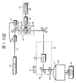
WO2010074190A1 - Objet microfabriqué, son procédé de fabrication et dispositif de gravure - Google Patents
Objet microfabriqué, son procédé de fabrication et dispositif de gravure Download PDFInfo
- Publication number
- WO2010074190A1 WO2010074190A1 PCT/JP2009/071520 JP2009071520W WO2010074190A1 WO 2010074190 A1 WO2010074190 A1 WO 2010074190A1 JP 2009071520 W JP2009071520 W JP 2009071520W WO 2010074190 A1 WO2010074190 A1 WO 2010074190A1
- Authority
- WO
- WIPO (PCT)
- Prior art keywords
- master
- shape
- optical element
- resist layer
- etching
- Prior art date
Links
Images


Classifications
-
- G—PHYSICS
- G02—OPTICS
- G02B—OPTICAL ELEMENTS, SYSTEMS OR APPARATUS
- G02B1/00—Optical elements characterised by the material of which they are made; Optical coatings for optical elements
- G02B1/10—Optical coatings produced by application to, or surface treatment of, optical elements
- G02B1/11—Anti-reflection coatings
- G02B1/118—Anti-reflection coatings having sub-optical wavelength surface structures designed to provide an enhanced transmittance, e.g. moth-eye structures
Definitions
- the present invention relates to a finely processed body, a manufacturing method thereof, and an etching apparatus used for manufacturing the same. Specifically, the present invention relates to a fine processed body having a curved surface.
- the concave-convex shape is rectangular, for a single wavelength light corresponding to the pitch, depth, etc. Effective antireflection effect can be obtained.
- the inventors of the present invention have proposed a method that combines an optical disc mastering process and an etching process as a method of manufacturing such a finely processed body (see, for example, Japanese Patent Application Laid-Open No. 2008-176076). In this method, a bell-shaped or elliptic frustum-shaped structure can be formed.
- the concavo-convex pattern is produced as follows.
- a solution obtained by diluting a resist, which is a photosensitive material, with a thinner is applied onto a smooth glass substrate by a spin coating method to form a smooth resist film with a uniform film thickness on the substrate.
- various exposure patterns are recorded and developed on the resist film of the substrate by an optical recording apparatus.
- a concavo-convex pattern having a uniform depth and width is formed.
- an object of the present invention is to provide a fine processed body having a fine uneven pattern on a curved surface such as a spherical surface or a cylindrical surface, a manufacturing method thereof, and an etching apparatus used for the manufacturing thereof.
- the first invention Forming an inorganic resist layer on a master having a curved surface; Exposing and developing the inorganic resist layer formed on the master, and forming a pattern on the inorganic resist layer; and A master with a pattern formed on an inorganic resist layer is placed on an electrode that has a curved surface that is almost the same as or similar to the curved surface of the master, and the master is etched to form a concavo-convex shape on the surface of the master.
- a process for producing the finely processed body is produced by a master having a curved surface.
- the second invention is A substrate having a curved surface; A structure that is a convex portion or a concave portion formed on the curved surface of the base body, The structure is a microfabricated body in which the structures are arranged at a pitch equal to or less than the wavelength of light under the usage environment.
- the third invention is An etching reaction tank; A first electrode and a second electrode disposed opposite to each other in an etching reaction tank; The first electrode has an arrangement surface on which the substrate is arranged; In the etching apparatus, the arrangement surface has a curved surface or an uneven surface.
- the fourth invention is: A substrate; A large number of structures arranged on the surface of the substrate, The structure is arranged at a pitch equal to or less than the wavelength of the light in the use environment, An optical element in which the structure is formed obliquely in two or more different directions with a predetermined angle with respect to the normal direction of the surface of the substrate.
- the tetragonal lattice means a regular tetragonal lattice.
- a quasi-tetragonal lattice means a distorted regular tetragonal lattice unlike a regular tetragonal lattice.
- the quasi-tetragonal lattice means a tetragonal lattice in which a regular tetragonal lattice is distorted by stretching in a linear arrangement direction.
- the quasi-tetragonal lattice is a tetragonal lattice in which a regular tetragonal lattice is distorted in an arc shape, or a regular tetragonal lattice is distorted in an arc shape, and This refers to a tetragonal lattice stretched and distorted in an arcuate arrangement direction.
- the hexagonal lattice means a regular hexagonal lattice.
- the quasi-hexagonal lattice means a distorted regular hexagonal lattice unlike a regular hexagonal lattice.
- the quasi-hexagonal lattice means a hexagonal lattice in which a regular hexagonal lattice is stretched and distorted in a linear arrangement direction.
- a quasi-hexagonal lattice is a hexagonal lattice in which a regular hexagonal lattice is distorted in an arc shape, or a regular hexagonal lattice is distorted in an arc shape, and This refers to a hexagonal lattice stretched and distorted in an arcuate arrangement direction.
- the master on which the inorganic resist pattern is formed is disposed on an electrode having a curved surface that is substantially the same as or similar to the curved surface of the master, and the master is etched, so that the master is etched in a direction perpendicular to the curved surface of the master. be able to. Therefore, an uneven pattern having a uniform depth and width can be formed on a master having a curved surface such as a cylinder or a sphere.
- FIG. 1A is a schematic plan view showing an example of the configuration of an optical element according to the first embodiment of the present invention.
- FIG. 1B is an enlarged plan view showing a part of the optical element shown in FIG. 1A.
- 1C is a cross-sectional view taken along tracks T1, T3,... Of FIG.
- FIG. 1D is a cross-sectional view taken along tracks T2, T4,...
- FIG. 2 is an enlarged perspective view showing a part of the optical element shown in FIG.
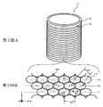
- FIG. 3A is a perspective view showing an example of the configuration of the master
- FIG. 3B is an enlarged plan view showing a part of the master shown in FIG. 3A.
- FIG. 4 is a schematic view showing an example of the configuration of an exposure apparatus for producing a master.
- FIG. 4 is a schematic view showing an example of the configuration of an exposure apparatus for producing a master.
- FIG. 5 is a schematic view showing an example of the configuration of an etching apparatus for producing a master.
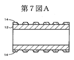
- FIGS. 6A to 6C are process diagrams for explaining a method of manufacturing an optical element according to the first embodiment of the present invention.
- FIGS. 7A to 7C are process diagrams for explaining the method of manufacturing an optical element according to the first embodiment of the present invention.
- FIG. 8 is a schematic view showing an example of the configuration of an exposure apparatus used for manufacturing an optical element according to the second embodiment of the present invention.
- FIG. 9 is a schematic view showing an example of the configuration of an exposure apparatus used for manufacturing an optical element according to the second embodiment of the present invention.
- FIG. 10A is a schematic plan view showing an example of the configuration of an optical element according to the fourth embodiment of the present invention.
- FIG. 10B is an enlarged plan view showing a part of the optical element shown in FIG. 10A.
- FIG. 10C is a sectional view taken along tracks T1, T3,...
- FIG. 10D is a sectional view taken along tracks T2, T4,...
- FIG. 11A is a schematic plan view showing an example of the configuration of an optical element according to the fifth embodiment of the present invention.
- FIG. 11B is an enlarged plan view showing a part of the optical element shown in FIG. 12A.
- FIG. 11C is a sectional view taken along tracks T1, T3,... Of FIG.
- FIG. 11D is a sectional view taken along tracks T2, T4,...
- FIG. 12A is a side view showing an example of the configuration of the master.
- FIG. 12A is a side view showing an example of the configuration of the master.
- FIG. 12B is an enlarged plan view showing a part of the master shown in FIG. 12A.
- FIG. 13 is a schematic view showing an example of the configuration of an exposure apparatus for producing a master.
- FIG. 14 is a schematic view showing an example of the configuration of an etching apparatus for producing a master.
- FIG. 15A is a schematic plan view showing an example of the configuration of an optical element according to the sixth embodiment of the present invention.
- FIG. 15B is an enlarged plan view showing a part of the optical element shown in FIG. 15A.
- FIG. 15C is a sectional view taken along tracks T1, T3,... Of FIG.
- FIG. 15D is a sectional view taken along tracks T2, T4,... Of FIG.
- FIG. 16 is an enlarged perspective view showing a part of the optical element shown in FIG. FIG.
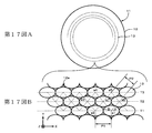
- FIG. 17A is a plan view showing an example of the configuration of the master.
- FIG. 17B is an enlarged plan view showing a part of the master shown in FIG. 17A.
- FIG. 18 is a schematic view showing an example of the configuration of an exposure apparatus for producing a master.
- FIG. 19 is a schematic view showing an example of the configuration of an etching apparatus for producing a master.
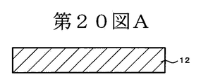
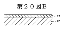
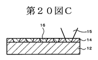
- FIGS. 20A to 20C are process diagrams for explaining a method of manufacturing an optical element according to the sixth embodiment of the present invention.
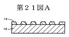
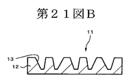
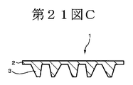
- 21A to 21C are process diagrams for explaining a method for manufacturing an optical element according to the sixth embodiment of the present invention.
- FIG. 22A is a schematic plan view showing an example of the configuration of an optical element according to the seventh embodiment of the present invention.
- FIG. 22B is an enlarged plan view showing a part of the optical element shown in FIG. 22A.
- 22C is a cross-sectional view taken along tracks T1, T3,...
- FIG. 22D is a sectional view taken along tracks T2, T4,...
- FIG. 23 is an enlarged perspective view showing a part of the optical element shown in FIG.
- FIG. 24 is a sectional view showing an example of the configuration of the liquid crystal display device according to the ninth embodiment of the present invention.
- FIG. 25 is a sectional view showing an example of the structure of the liquid crystal display device according to the tenth embodiment of the present invention.
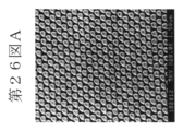
- FIG. 26A is a SEM photograph of the optical element of Example 1.
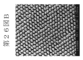
- FIG. 26B is a SEM photograph of the optical element of Example 2.
- FIG. 26A is a SEM photograph of the optical element of Example 1.
- FIG. 26B is a SEM photograph of the optical element of Example 2.
- FIG. 26A is a SEM photograph of the optical element of Example 1.
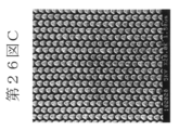
- FIG. 26C is a SEM photograph of the optical element of Example 3.
- FIG. 27 is a graph showing the antireflection characteristics of Example 1.
- FIG. 28A is a perspective view showing an appearance of a moth-eye lens film of Example 4.
- FIG. 28B is a sectional view taken along line AA in FIG. 28A.
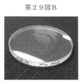
- FIGS. 29A and 29B are photographs showing the appearance of the moth-eye quartz lens of Example 5.
- FIG. 1A is a schematic plan view showing an example of the configuration of an optical element according to the first embodiment of the present invention.
- FIG. 1B is an enlarged plan view showing a part of the optical element shown in FIG. 1A.
- 1C is a cross-sectional view taken along tracks T1, T3,... Of FIG.
- FIG. 1D is a cross-sectional view taken along tracks T2, T4,...
- the optical element 1 is suitable for application to various optical components such as a display, optoelectronics, optical communication (optical fiber), solar cell, and lighting device.
- the optical element 1 includes a base 2 and a structure 3 that is a convex portion formed on the surface of the base 2.
- the optical element 1 has a function of preventing reflection of light incident on the surface of the substrate on which the structure 3 is provided.
- X axis and Y axis two axes orthogonal to each other in one main surface of the base 2 are referred to as X axis and Y axis, and an axis perpendicular to one main surface of the base 2 is referred to as Z axis.
- the substrate 2 is a transparent substrate having transparency.
- the material of the base 2 include transparent synthetic resins such as polycarbonate (PC) and polyethylene terephthalate (PET), and materials mainly composed of glass, but are not particularly limited to these materials.
- the shape of the substrate 2 include a film shape, a sheet shape, a plate shape, and a block shape, but are not particularly limited to these shapes.
- the shape of the base 2 is a main body portion of various optical devices that require a predetermined antireflection function such as a display, optoelectronics, optical communication, a solar cell, and a lighting device, and a sheet or film attached to these optical devices. It is preferable to select and decide according to the shape of the antireflection functional component.
- FIG. 2 is an enlarged perspective view showing a part of the optical element shown in FIG. A large number of structures 3 that are convex portions are arranged on the surface of the base 2.
- the structures 3 are periodically two-dimensionally arranged at a short pitch equal to or less than the wavelength of light under the usage environment, for example, at a pitch comparable to the wavelength of visible light.
- the light under the usage environment is, for example, ultraviolet light, visible light, or infrared light.
- ultraviolet light means light having a wavelength range of 10 nm or more and less than 360 nm
- visible light means light of 360 nm or more and 830 nm or less
- infrared light means light of more than 830 nm and 1 mm or less.
- the structure 3 of the optical element 1 has an arrangement form that forms a plurality of rows of tracks T1, T2, T3,... (Hereinafter collectively referred to as “tracks T”) on the surface of the base 2.
- the track refers to a portion where the structures 3 are arranged in a straight line in a row.
- the lower portions of the adjacent structures 3 may be overlapped to join the lower portions of the structures 3 together.
- the bonding of the structures 3 is performed by all or part of the structures 3 that are adjacent to each other.
- the lower portions of the structures 3 arranged in the track direction are overlapped and joined.
- the structure 3 is disposed at a position shifted by a half pitch between two adjacent tracks T.
- the structure of the other track for example, T2
- the intermediate position position shifted by a half pitch
- a hexagonal lattice pattern or a quasi-hexagonal lattice pattern in which the center of the structure 3 is located at each point a1 to a7 between adjacent three rows of tracks (T1 to T3) is formed.
- the structure 3 is arranged.
- the hexagonal lattice pattern means a regular hexagonal lattice pattern.
- the quasi-hexagonal lattice pattern is a distorted hexagonal lattice pattern that is stretched in the track extending direction (X-axis direction), unlike a regular hexagonal lattice pattern.
- the distance is the arrangement pitch of the structures 3 between two adjacent tracks (for example, T1 and T2), that is, the arrangement pitch P2 of the structures 3 in the ⁇ ⁇ directions (for example, a1 to a7,. It is preferable that the distance is longer than (distance between a2 to a7).
- the height of the structure 3 is not particularly limited, and is appropriately set according to the wavelength region of light to be transmitted.
- the height of the structure 3 is, for example, 236 nm to 450 nm, preferably 415 nm to 421 nm.
- the aspect ratio (height H / arrangement pitch P) of the structures 3 is preferably set in the range of 0.81 to 1.46. If it is less than 0.81, the reflection characteristics and the transmission characteristics tend to be reduced, and if it exceeds 1.46, the peeling characteristics are lowered during the production of the optical element 1, and the replica tends to be unrecoverable. It is.
- the aspect ratio is defined by the following formula (1).
- Aspect ratio H / P (1)
- H Height of the structure 3
- P Average arrangement pitch (average period)
- the average arrangement pitch P is defined by the following equation (2).
- Average arrangement pitch P (P1 + P2 + P2) / 3 (2)
- P1 arrangement pitch in the track extending direction (track extending direction period)
- the height H of the structures 3 is the height H2 of the structures 3 in the column direction (see FIG. 2).
- the column direction means a direction (Y-axis direction) orthogonal to the track extending direction (X-axis direction) in the substrate surface.
- the height H1 in the track extending direction of the structure 3 is smaller than the height H2 in the column direction.
- the height of the structure 3 in a portion other than the track extending direction is substantially the same as the height H2 in the column direction.
- the height H of the structures 3 is represented by the height H2 in the column direction.
- the structures 3 have the same shape, but the shape of the structure 3 is not limited to this, and two or more types of structures 3 are formed on the surface of the substrate. May be.
- the structure 3 may be formed integrally with the base 2.
- the aspect ratios of the structures 3 are not limited to the same, and the structures 3 are configured to have a certain height distribution (for example, an aspect ratio in the range of about 0.83 to 1.46). Also good.
- the height distribution means that the structures 3 having two or more heights (depths) are provided on the surface of the base 2. That is, it means that the structure 3 having a reference height and the structure 3 having a height different from the structure 3 are provided on the surface of the base 2.
- the structures 3 having a height different from the reference are provided, for example, on the surface of the base 2 periodically or non-periodically (randomly).
- the material of the structure 3 is preferably, for example, an ionizing radiation curable resin that is cured by ultraviolet rays or electron beams, or a thermosetting resin that is cured by heat, and an ultraviolet curable resin that can be cured by ultraviolet rays.
- the main component is most preferable.
- the structure 3 preferably has a curved surface that gradually spreads from the top to the bottom of the structure 3. This is because transferability can be improved by using such a shape.
- the top of the structure 3 is, for example, a flat surface or a convex curved surface, preferably a convex curved surface.
- a low refractive index layer having a lower refractive index than that of the structure 3 may be formed on the top of the structure 3, and by forming such a low refractive index layer, the reflectance can be lowered.
- the overall shape of the structure 3 include a cone shape.
- the cone shape include a cone shape, a truncated cone shape, an elliptical cone shape, an elliptical truncated cone shape, a cone shape having a curvature at the top portion, and an elliptic cone shape having a curvature at the top portion.
- the cone shape includes an elliptical cone shape, an elliptical truncated cone shape, a cone shape with a curvature at the top, and an elliptic cone shape with a curvature at the top. It is a concept that includes. Further, the truncated cone shape refers to a shape obtained by cutting off the top portion of the truncated cone shape, and the elliptical truncated cone shape refers to a shape obtained by cutting off the top portion of the elliptical cone. Note that the overall shape of the structure 3 is not limited to these shapes, and can be appropriately selected according to desired characteristics.
- the structure 3 having an elliptical cone shape is an elliptical, oval or egg-shaped cone structure having a bottom surface having a major axis and a minor axis, and a top portion having a curved surface.
- the structure 3 having an elliptical truncated cone shape is an elliptical, oval or egg-shaped pyramid structure with a bottom surface having a major axis and a minor axis, and a top portion is flat.
- the structure 3 is formed on the substrate surface so that the major axis direction of the bottom surface of the structure 3 is the track extending direction (X-axis direction).
- FIG. 3 shows an example of the configuration of a master for producing an optical element having the above-described configuration.
- the master 11 is a so-called roll master, and has a structure in which a large number of structures 13 that are concave portions are arranged on the surface of a cylindrical master 12.
- the structures 13 are periodically two-dimensionally arranged at a pitch equal to or less than the wavelength of light in the environment in which the optical element 1 is used, for example, the wavelength of visible light.
- the structure 13 is arranged concentrically or spirally on the surface of the columnar master 12.
- the structure 13 is for forming the structure 3 that is a convex portion on the surface of the base 2 described above.
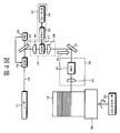
- FIG. 4 is a schematic view showing an example of the configuration of an exposure apparatus for producing a master having the above-described configuration.
- This exposure apparatus is configured based on an optical disk recording apparatus.
- the laser light 15 emitted from the laser light source 21 travels straight as a parallel beam and enters an electro-optic element (EOM: Electro Optical Modulator) 22.
- EOM Electro Optical Modulator
- the laser beam 15 transmitted through the electro-optical element 22 is reflected by the mirror 23 and guided to the modulation optical system 25.
- the mirror 23 is composed of a polarization beam splitter and has a function of reflecting one polarization component and transmitting the other polarization component.
- the polarized light component transmitted through the mirror 23 is received by the photodiode 24, and the electro-optic element 22 is controlled based on the received light signal, and the phase modulation of the laser light 15 is performed.
- the laser beam 15 is transmitted through a condenser lens 26 to glass (SiO 2). 2 ) Or the like, the light is condensed on an AOM (Acoustic-Optic Modulator) 27.
- AOM Acoustic-Optic Modulator
- the laser beam 15 is intensity-modulated by the acousto-optic element 27 and diverges, and then converted into a parallel beam by the collimator lens 28.
- the laser beam 15 emitted from the modulation optical system 25 is reflected by the mirror 31 and guided horizontally and in parallel on the moving optical table 32.
- the moving optical table 32 includes a beam expander 33 and an objective lens 34.
- the laser light 15 guided to the moving optical table 32 is shaped into a desired beam shape by the beam expander 33 and then irradiated to the resist layer on the master 12 through the objective lens 34.
- the master 12 is placed on a turntable 36 connected to a spindle motor 35.
- the resist layer is exposed by intermittently irradiating the resist layer with the laser beam 15 while rotating the master 12 and moving the laser beam 15 in the height direction of the master 12.
- the formed latent image has, for example, a substantially elliptical shape having a major axis in the circumferential direction.
- the laser beam 15 is moved by moving the moving optical table 32 in the arrow R direction.
- the exposure apparatus includes a control mechanism 37 for forming a latent image corresponding to the two-dimensional pattern of the hexagonal lattice or the quasi-hexagonal lattice shown in FIG. 1B on the resist layer.
- the control mechanism 37 includes a formatter 29 and a driver 30.
- the formatter 29 includes a polarity reversal unit, and this polarity reversal unit controls the irradiation timing of the laser beam 15 on the resist layer.
- the driver 30 receives the output from the polarity inversion unit and controls the acoustooptic device 27.
- a signal is generated by synchronizing the polarity inversion formatter signal and the rotation controller of the recording apparatus for each track so that the two-dimensional pattern is spatially linked, and the intensity is modulated by the acoustooptic device 27. .
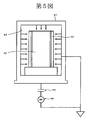
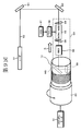
- FIG. 5 is a schematic view showing an example of the configuration of an etching apparatus for producing a master having the above-described configuration.
- the etching apparatus is a so-called RIE (Reactive Ion Etching) apparatus.
- RIE Reactive Ion Etching
- the cylindrical electrode 42 is disposed in the center of the etching reaction tank 41.
- a counter electrode 43 is provided inside the etching reaction tank 41.
- the columnar electrode 42 has a configuration in which the cylindrical master 12 can be attached and detached.
- the columnar electrode 42 has, for example, a columnar surface that is substantially the same or similar to the cylindrical surface of the cylindrical master 12, specifically, a columnar surface having a slightly smaller diameter than the inner peripheral surface of the cylindrical master 12.
- the cylindrical electrode 43 is connected to a high frequency power supply (RF) 45 of 13.56 MHz, for example, via a blocking capacitor 44.
- the counter electrode 43 is connected to the ground.
- etching apparatus having the above-described configuration, when a high frequency voltage is applied between the counter electrode 43 and the cylindrical electrode 42 by the high frequency power supply 45, plasma is generated between the counter electrode 43 and the cylindrical electrode 42. Since the counter electrode 43 is connected to the ground, the potential does not change. On the other hand, the cylindrical electrode 42 has a negative potential because the circuit is blocked by the blocking capacitor 44, and a voltage drop occurs. Due to this voltage drop, an electric field is generated in a direction perpendicular to the cylindrical surface of the cylindrical electrode 42, and positive ions in the plasma are incident perpendicularly to the outer peripheral surface of the cylindrical master 12 and anisotropic etching is performed.
- the method for manufacturing an optical element according to the first embodiment is a method in which an optical disc master production process and an etching process are combined.
- the manufacturing method includes a resist film forming step for forming a resist layer on the master, an exposure step for forming a latent image on the resist layer using an exposure apparatus, a developing step for developing the resist layer on which the latent image is formed, An etching process for manufacturing a master by etching and a replication process for manufacturing a replication substrate by an ultraviolet curable resin are provided.
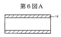
- a cylindrical master 12 is prepared.
- the master 12 is, for example, a glass master.
- an inorganic resist layer 14 is formed on the outer peripheral surface of the cylindrical master 12 by sputtering.
- the inorganic resist for example, a metal oxide made of one or more transition metals such as tungsten and molybdenum can be used.
- the master 12 is rotated and the laser beam (exposure beam) 15 is irradiated to the inorganic resist layer 14 using the exposure apparatus shown in FIG.
- the inorganic resist layer 14 is exposed over the entire surface by intermittently irradiating the laser beam 15 while moving the laser beam 15 in the height direction of the master 12.
- the latent image 16 according to the locus of the laser beam 15 is formed over the entire surface of the inorganic resist layer 14 at a pitch similar to the visible light wavelength, for example.
- a developer is dropped on the inorganic resist layer 14 to develop the inorganic resist layer 14 as shown in FIG. 7A.
- the exposed portion exposed with the laser beam 15 has a higher dissolution rate with respect to the developer than the non-exposed portion. Therefore, as shown in FIG. 7A.
- a pattern corresponding to the latent image (exposed portion) 16 is formed on the inorganic resist layer 14. (Etching process)
- the surface of the master 12 is etched using the pattern (resist pattern) of the inorganic resist layer 14 formed on the master 12 as a mask. Thereby, as shown in FIG.
- the structure 13 for example, an elliptical cone-shaped or elliptical truncated cone-shaped recess having the major axis direction in the track extending direction, that is, the structure 13 can be obtained. Moreover, you may make it perform an etching process and an ashing process alternately as needed. By doing in this way, the structure 13 which has a various curved surface can be formed. For example, by alternately repeating ashing and etching, and gradually increasing the etching time, the shape of the structure 3 can be changed to an elliptical cone having a gentle slope at the top and a gradually steep slope from the center to the bottom. Can be shaped.
- a glass master having a depth three times or more of the inorganic resist layer 14 (selection ratio 3 or more) can be produced, and the structure 3 can have a high aspect ratio.
- the master 11 having a hexagonal lattice pattern or a quasi-hexagonal lattice pattern is obtained.
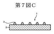
- the master 11 and the substrate 2 such as an acrylic sheet coated with an ultraviolet curable resin are brought into close contact with each other, irradiated with ultraviolet rays to cure the ultraviolet curable resin, and then the substrate 2 is peeled from the master 11. Thereby, as shown in FIG. 7C, the target optical element 1 is manufactured.
- the inorganic resist layer 14 is formed by the sputtering method, a smooth inorganic resist film having a uniform film thickness can be formed on the surface of the cylindrical master 12.
- the cylindrical master 12 is disposed on the column electrode 42 and reactive ion etching is performed, positive ions can be incident on the outer peripheral surface of the cylindrical master 12 perpendicularly to perform anisotropic etching.
- an uneven pattern having a uniform depth and width can be formed on the master 12 having a cylindrical surface.
- the optical element 1 is manufactured by using a method in which an optical disk master production process and an etching process are combined, the master disk production process is performed as compared with the case where the optical element 1 is produced using electron beam exposure.
- the time required (exposure time) can be greatly reduced. Therefore, the productivity of the optical element 1 can be greatly improved. Further, when the shape of the top of the structure 3 is not sharp but smooth, for example, a smooth curved surface protruding in the height direction, the durability of the optical element 1 can be improved. Moreover, the peelability of the optical element 1 with respect to the master 11 can also be improved.
- the process of forming an organic resist film by a general spin coating method when the master has a curved surface (cylindrical or spherical), uneven coating occurs, and it is difficult to form a smooth resist film with a uniform film thickness. It is. Therefore, it is difficult to form an uneven pattern having a uniform depth and width on the curved master surface.
- the inorganic resist layer 14 is formed by sputtering, a smooth inorganic resist film having a uniform film thickness can be formed on the surface of the cylindrical master 12. Therefore, an uneven pattern having a uniform depth and width can be formed on the curved master surface. Further, by applying the above-described manufacturing method, it is possible to form a concavo-convex pattern having a uniform depth and width in addition to a master having a curved surface such as a cylinder or a sphere. For example, an uneven pattern having a uniform depth and width can be formed on a master such as a sheet, tape, bar, needle, rectangular parallelepiped (box), wire frame, or cylinder.
- a master such as a sheet, tape, bar, needle, rectangular parallelepiped (box), wire frame, or cylinder.
- FIG. 8 is a schematic view showing an example of the configuration of an exposure apparatus used for manufacturing an optical element according to the second embodiment of the present invention. As shown in FIG. 8, the second embodiment is different from the first embodiment in that exposure is performed with a cylindrical master 12 lying sideways.
- This exposure apparatus includes a turntable 60, a spindle servo 61, a laser light source 51 (266 nm), a mirror M1 and a mirror M2, a drive circuit (driver) 58, a moving optical table 53, a voltage frequency controller 57, an air slider (not shown). ), A feed servo (not shown), and a focus servo (not shown) of a defocusing method (skew method) are provided as main parts.
- the light source for exposure is not limited to such a laser light source 51 in particular.
- the laser light 52 emitted from the laser light source 51 travels straight as a parallel beam, is reflected by the mirror M1 and the mirror M2, changes its direction, and is guided to the moving optical table 53.
- two wedge prisms 54 and one acousto-optic modulation deflector (AOM / AOD; Acoustic Optical Modulator / Acoustic Optical Defector) 55 are arranged on the moving optical table 53.
- the wedge prism 54 and the acousto-optic modulation deflector 55 are arranged so that the laser beam 52 and the grating surface incident as parallel beams satisfy the Bragg condition and the beam horizontal height does not change.
- quartz (SiO 2 ) As an acoustooptic device used for the acoustooptic modulation deflector 55, quartz (SiO 2 ) Is preferred.
- a predetermined signal is supplied from the drive circuit 58 to the acousto-optic modulation deflector 55.
- the drive circuit 58 is supplied with a high frequency signal from a voltage frequency controller (VCO) 57.
- a control signal is supplied to the voltage frequency controller 57.
- the acousto-optic modulation deflector 55 utilizes the fact that the first-order diffracted light intensity in Bragg diffraction is substantially proportional to the ultrasonic power, and modulates the ultrasonic power based on the recording signal to modulate the laser light 52. And a predetermined exposure pattern is formed.
- the positional relationship and attitude of the acousto-optic modulation deflector 55 with respect to the optical axis of the laser beam 52 are set.
- FIG. 9 is a schematic view showing an example of the configuration of an exposure apparatus used for manufacturing an optical element according to the second embodiment of the present invention. As shown in FIG.
- FIG. 10A is a schematic plan view showing an example of the configuration of an optical element according to the fourth embodiment of the present invention.
- FIG. 10B is an enlarged plan view showing a part of the optical element shown in FIG. 10A.
- FIG. 10C is a sectional view taken along tracks T1, T3,...
- FIG. 10D is a sectional view taken along tracks T2, T4,... Of FIG.
- the optical element 1 according to the fourth embodiment is different from that of the first embodiment in that the structure 3 forms a tetragonal lattice pattern or a quasi-tetragonal lattice pattern between adjacent three rows of tracks. ing.
- the quasi-tetragonal lattice pattern means a distorted tetragonal lattice pattern that is stretched in the track extending direction (X-axis direction).
- the structures 3 are periodically arranged in a tetragonal lattice pattern or a quasi-tetragonal lattice pattern, for example, the structures 3 are adjacent to each other in an orientation that is four-fold symmetric.
- the structure 3 of the other track (for example, T2) is arranged at an intermediate position (position shifted by a half pitch) of the structures 3 arranged on one track (for example, T1). Yes. As a result, as shown in FIG.
- a tetragonal lattice pattern or a quasi-tetragonal lattice pattern in which the center of the structure 3 is located at each point a1 to a4 between adjacent three rows of tracks (T1 to T3) is formed.
- the structure 3 is arranged.
- the height (depth) of the structure 3 is not particularly limited, and is appropriately set according to the wavelength region of light to be transmitted. For example, when visible light is transmitted, the height (depth) of the structure 3 is preferably 150 nm to 500 nm.
- the pitch P2 in the ⁇ direction with respect to the track T is, for example, about 275 nm to 297 nm.
- the aspect ratio (height H / arrangement pitch P) of the structures 3 is, for example, about 0.54 to 1.13. Furthermore, the aspect ratios of the structures 3 are not limited to the same, and the structures 3 may be configured to have a certain height distribution.
- the arrangement pitch P1 of the structures 3 in the same track is preferably longer than the arrangement pitch P2 of the structures 3 between two adjacent tracks.
- the ratio P1 / P2 is 1.4 ⁇ P1 / P2 ⁇ 1. It is preferable that the relationship 5 is satisfied.
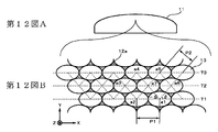
- FIG. 11A is a schematic plan view showing an example of the configuration of an optical element according to the fifth embodiment of the present invention.
- FIG. 11B is an enlarged plan view showing a part of the optical element shown in FIG. 12A.
- FIG. 11C is a sectional view taken along tracks T1, T3,... Of FIG. FIG.
- FIG. 11D is a sectional view taken along tracks T2, T4,...
- the optical element 1 according to the fifth embodiment is different from the first embodiment in that the optical element 1 has a spherical surface and the structure 3 is formed on the spherical surface.
- the spherical surface is, for example, a convex or concave spherical surface.
- the optical element 1 is, for example, a concave lens or a convex lens.
- FIG. 11 shows an example in which the optical element 1 has a concave spherical surface.
- the optical element 1 according to the fifth embodiment is the same as the first embodiment except for the above.
- FIG. 12 shows an example of the configuration of a master for producing an optical element having the above-described configuration.
- the master 11 according to the fifth embodiment is different from the first embodiment in that it has a spherical surface and the structure 13 is formed on the spherical surface.
- the spherical surface is, for example, a convex or concave spherical surface.
- FIG. 12 the case where the master 11 has a convex spherical surface is shown as an example.
- the master 11 according to the fifth embodiment is the same as the first embodiment except for the above.
- FIG. 13 is a schematic view showing an example of the configuration of an exposure apparatus for producing a master having the above-described configuration.
- the moving optical table 32 includes a beam expander 33, a mirror 38, and an objective lens 34.
- a position sensor (not shown) is provided at a position directly below the objective lens 34. By this position sensor, collision with the spherical surface of the master 12 is prevented.
- the laser beam 15 guided to the moving optical table 32 is shaped into a desired beam shape by the beam expander 33, and then passes through the mirror 38 and the objective lens 34 to the resist layer formed on the spherical surface of the master 12. Irradiated.
- the master 12 having a spherical surface is placed on a turntable 36 connected to a spindle motor 35. Then, while rotating the master 12 and moving the laser beam 15 in the rotational radius direction of the master 12, the resist layer on the master 12 is intermittently irradiated with the laser beam, whereby the resist layer exposure process is performed. .
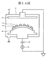
- FIG. 14 is a schematic view showing an example of the configuration of an etching apparatus for producing a master having the above-described configuration.
- a spherical electrode 46 and a counter electrode 47 facing the spherical electrode 46 are provided in the etching reaction tank 41.
- the spherical electrode 46 has a spherical surface on the side facing the counter electrode 47, and the master 12 is placed on this spherical surface.
- the spherical electrode 46 is configured so that the spherical master 12 can be attached and detached.
- FIG. 15A is a schematic plan view showing an example of the configuration of an optical element according to the sixth embodiment of the present invention.
- FIG. 15B is an enlarged plan view showing a part of the optical element shown in FIG. 15A.
- FIG. 15C is a sectional view taken along tracks T1, T3,... Of FIG.
- FIG. 15D is a sectional view taken along tracks T2, T4,... Of FIG. FIG.
- FIG. 16 is an enlarged perspective view showing a part of the optical element shown in FIG.
- the sixth embodiment is different from the first embodiment in that the structure 3 is inclined with respect to the substrate surface.
- the structure 3 may face two or more different directions with respect to the substrate surface.
- the structure 3 may be formed obliquely in two or more different directions with a predetermined angle with respect to the normal direction of the substrate surface, for example.
- the structure 3 may have a plurality of regions, and the direction of the structure may be different depending on each region.
- the optical element according to the sixth embodiment is the same as the first embodiment except for the above.
- FIG. 17 shows an example of the configuration of a master for producing an optical element having the above-described configuration. As shown in FIG.
- the master 11 has a structure in which a large number of structures 13 that are concave portions are arranged on the surface of a disk-shaped master 12.
- the structures 13 are periodically two-dimensionally arranged at a pitch equal to or less than the wavelength of light in the environment in which the optical element 1 is used, for example, the wavelength of visible light.
- the structure 13 is disposed on, for example, a concentric or spiral track.
- the master according to the sixth embodiment is the same as the first embodiment except for the above.
- FIG. 18 is a schematic view showing an example of the configuration of an exposure apparatus for producing a master having the above-described configuration.
- the exposure apparatus according to the sixth embodiment is the same as that of the fifth embodiment. However, in the sixth embodiment, as shown in FIG.
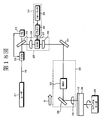
- FIG. 19 is a schematic view showing an example of the configuration of an etching apparatus for producing a master having the above-described configuration.
- an uneven surface electrode 48 and a counter electrode 47 facing the uneven surface electrode 48 are provided in the etching reaction tank 41.
- the uneven surface electrode 48 has an uneven surface on the side facing the counter electrode 47, and the master 12 is placed on the uneven surface.
- the master 12 can be anisotropically etched in two or more different directions using the concavo-convex surface of the concavo-convex surface electrode 48.
- the concavo-convex shape of the concavo-convex surface electrode 48 it is possible to change the direction of anisotropic etching according to the surface area of the master 12 using the concavo-convex surface of the concavo-convex surface electrode 48. is there.
- the etching apparatus according to the sixth embodiment is the same as the first embodiment except for the above.
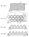
- FIG. 20A a disk-shaped master 12 is prepared.
- the master 12 is, for example, a glass master.
- an inorganic resist layer 14 is formed on one main surface of the disk-shaped master 12 by a sputtering method.
- the inorganic resist for example, a metal oxide made of one or more transition metals such as tungsten and molybdenum can be used.
- the master 12 is rotated and the inorganic resist layer 14 is irradiated with a laser beam (exposure beam) 15 using the exposure apparatus shown in FIG.
- the inorganic resist layer 14 is exposed over the entire surface by intermittently irradiating the laser beam 15 while moving the laser beam 15 in the height direction of the master 12.
- the latent image 16 according to the locus of the laser beam 15 is formed over the entire surface of the inorganic resist layer 14 at a pitch similar to the visible light wavelength, for example.
- a developer is dropped on the inorganic resist layer 14 to develop the inorganic resist layer 14 as shown in FIG. 21A.
- the exposed portion exposed with the laser beam 15 has a higher dissolution rate with respect to the developer than the non-exposed portion. Therefore, as shown in FIG. 21A.
- a pattern corresponding to the latent image (exposed portion) 16 is formed on the inorganic resist layer 14.
- the surface of the master 12 is etched using the pattern (resist pattern) of the inorganic resist layer 14 formed on the master 12 as a mask.
- a structure 13 is formed that is directed in various directions such as an oblique direction with respect to one main surface of the disk-shaped master 12.
- the structure 13 which has a various curved surface can be formed.
- the master 11 in which the structure 3 is formed in an oblique direction with respect to the substrate surface is obtained.
- the master 11 and the substrate 2 such as an acrylic sheet coated with an ultraviolet curable resin are brought into close contact with each other, irradiated with ultraviolet rays to cure the ultraviolet curable resin, and then the substrate 2 is peeled from the master 11.
- the target optical element 1 is manufactured.
- FIG. 22A is a schematic plan view showing an example of the configuration of an optical element according to the seventh embodiment of the present invention.
- FIG. 22B is an enlarged plan view showing a part of the optical element shown in FIG. 22A.
- 19C is a cross-sectional view taken along tracks T1, T3,... Of FIG. 22D is a cross-sectional view taken along tracks T2, T4,... Of FIG.
- FIG. 23 is an enlarged perspective view showing a part of the optical element shown in FIG.
- the optical element 1 according to the seventh embodiment is different from that of the first embodiment in that a large number of structures 3 that are concave portions are arranged on the surface of the substrate.
- the shape of the structure 3 is a concave shape obtained by inverting the convex shape of the structure 3 in the first embodiment.
- the eighth embodiment is different from the first embodiment in that an inorganic resist layer 14 is developed to form a concavo-convex pattern and is directly used as a master.
- an optical element is produced as follows. First, the steps from the resist film formation step to the development step are performed in the same manner as in the first embodiment. Thereby, concave portions of a hexagonal lattice pattern or a quasi-hexagonal lattice pattern are formed in the inorganic resist layer 14. Next, the optical element 1 is manufactured as follows using the master 12 having such a pattern formed on the inorganic resist layer 14 as a master.
- the eighth embodiment is the same as the first embodiment except for the above.
- a highly rigid inorganic resist layer 14 is formed on a master 12 such as a metal master or sheet by sputtering, and the inorganic resist layer 14 is exposed and developed to form an inorganic material.
- An uneven pattern is formed on the resist layer 14. Therefore, the master 12 having the uneven pattern of the inorganic resist layer 14 can be used directly as a stamper.
- FIG. 24 shows an example of the configuration of the liquid crystal display device according to the ninth embodiment of the present invention. As shown in FIG.
- this liquid crystal display device includes a backlight 73 that emits light, and a liquid crystal panel 71 that temporally and spatially modulates the light emitted from the backlight 73 to display an image.
- Polarizers 71a and 71b are provided on both surfaces of the liquid crystal panel 71, respectively.
- the optical element 1 is provided on the polarizer 71 b provided on the display surface side of the liquid crystal panel 71.
- the polarizer 71b in which the optical element 1 is provided on one main surface is referred to as a polarizer 72 with an antireflection function.
- This polarizer 72 with an antireflection function is an example of an optical component with an antireflection function.
- the backlight 73 for example, a direct backlight, an edge backlight, or a flat light source backlight can be used.
- the backlight 73 includes, for example, a light source, a reflecting plate, an optical film, and the like.
- the light source include a cold cathode fluorescent lamp (CCFL), a hot cathode fluorescent lamp (HCFL), an organic electroluminescence (OEL), an inorganic electroluminescence (OEL), and an inorganic electroluminescence (OEL).
- liquid crystal panel 71 for example, a twisted nematic (TN) mode, a super twisted nematic (STN) mode, a vertical alignment (Vertical Aligned: VA) mode, a horizontal alignment (In-Plane: Switch) is used.
- TN twisted nematic
- STN super twisted nematic
- VA vertical alignment
- VA horizontal alignment
- In-Plane: Switch horizontal alignment
- Mode optically compensated bend alignment
- CGH light emitting diode
- polarizers 71a and 71b are provided on both surfaces of the liquid crystal panel 71 so that their transmission axes are orthogonal to each other.
- the polarizers 71a and 71b allow only one of the orthogonal polarization components of incident light to pass through and shield the other by absorption.
- the polarizers 71a and 71b include hydrophilic polymer films such as polyvinyl alcohol films, partially formalized polyvinyl alcohol films, ethylene / vinyl acetate copolymer partially saponified films, iodine, dichroic dyes, and the like. Those obtained by adsorbing the dichroic substance and uniaxially stretching can be used.
- the protective layer is provided in this way, it is preferable that the base 2 of the optical element 1 also serves as the protective layer. This is because the polarizer 72 with an antireflection function can be thinned by adopting such a configuration.
- TAC triacetyl cellulose Since the optical element 1 is the same as any one of the first to fourth, sixth, and seventh embodiments described above, the description thereof is omitted. According to the ninth embodiment, since the optical element 1 is provided on the display surface of the liquid crystal display device, the antireflection function of the display surface of the liquid crystal display device can be improved.
- FIG. 25 shows an example of the configuration of the liquid crystal display device according to the tenth embodiment of the present invention.
- this liquid crystal display device includes a front member 74 on the front side of the liquid crystal panel 71, and the optical element 1 is provided on at least one of the front surface of the liquid crystal panel 71, the front surface and the back surface of the front member 74. Is different from that of the ninth embodiment.
- FIG. 25 shows an example in which the optical element 1 is provided on the front surface of the liquid crystal panel 71 and all the front and back surfaces of the front member 74.
- an air layer is formed between the liquid crystal panel 71 and the front member 74.
- the front surface refers to the surface on the side serving as the display surface, that is, the surface on the viewer side
- the back surface refers to the surface on the side opposite to the display surface.
- the front member 74 is a front panel or the like used for the purpose of mechanical, thermal, and weatherproof protection and design on the front surface (observer side) of the liquid crystal panel 71.
- the front member 74 has, for example, a sheet shape, a film shape, or a plate shape.
- Examples of the material of the front member 74 include glass, triacetyl cellulose (TAC), polyester (TPEE), polyethylene terephthalate (PET), polyimide (PI), polyamide (PA), aramid, polyethylene (PE), polyacrylate, Polyether sulfone, polysulfone, polypropylene (PP), diacetyl cellulose, polyvinyl chloride, acrylic resin (PMMA), polycarbonate (PC), and the like can be used, but the material is not particularly limited and is transparent. Any material having a property can be used. According to the tenth embodiment, the visibility of the liquid crystal display device can be improved as in the ninth embodiment.
- Example 1 First, an inorganic resist layer made of an oxide of tungsten (W) and molybdenum (Mo) was formed on a disk-shaped quartz substrate by a sputtering method. Next, a quasi-hexagonal lattice pattern latent image was formed on the inorganic resist layer using the exposure apparatus shown in FIG. Thereafter, the resist layer was subjected to development processing to produce a resist pattern. A 2.38% tetramethylammonium hydroxide aqueous solution (Tokyo Ohka Kogyo Co., Ltd.) was used as the developer.
- W tungsten
- Mo molybdenum
- Example 2 A duplicate substrate was obtained in the same manner as in Example 1 except that the uneven shape of the uneven electrode of the etching apparatus was changed.
- Example 3 First, a glass roll master having an outer diameter of 126 mm was prepared, and an inorganic resist layer made of an oxide of tungsten (W) and molybdenum (Mo) was formed on the surface of the glass roll master by a sputtering method.
- the glass roll master as a recording medium was conveyed to the exposure apparatus shown in FIG. 4 to expose the inorganic resist layer.
- a latent image forming a quasi-hexagonal lattice pattern between the adjacent three rows of tracks was patterned on the resist while continuing in one spiral shape.
- the inorganic resist layer on the glass roll master was subjected to development treatment, and the exposed portion of the resist was dissolved and developed.
- an undeveloped glass roll master is placed on a turntable of a developing machine (not shown), and a developer is dropped on the surface of the glass roll master while rotating the entire turntable to develop the resist on the surface. .
- a resist glass master having a resist layer opened in a quasi-hexagonal lattice pattern was obtained.
- the developer used was 2.38% tetramethylammonium hydroxide aqueous solution (Tokyo Ohka Kogyo Co., Ltd.).
- a process of etching the glass roll master by RIE etching and a process of removing the resist pattern by ashing and widening the opening diameter were repeated. Etching was performed using an etching apparatus having a cylindrical electrode shown in FIG.
- the quasi-hexagonal lattice pattern diameter at which the surface of the glass roll master is exposed gradually expands while etching proceeds in the direction perpendicular to the surface of the glass roll master, and the resist pattern is used as a mask in other areas. It was not etched. Thereby, the recessed part which goes to a perpendicular direction with respect to the surface of a glass roll original recording was formed. Finally, the resist pattern was completely removed by ashing. Thus, the intended glass roll master was obtained. Next, the produced glass roll master and an acrylic sheet coated with an ultraviolet curable resin were brought into close contact with each other, and peeled while being cured by irradiation with ultraviolet rays to produce an optical element.
- FIG. 26A and FIG. 26B show that the structure can be formed in an oblique direction with respect to the substrate by etching using the concavo-convex surface electrode. Moreover, it turns out that the direction of a structure can be changed according to an area
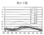
- FIG. 26C shows that a structure can be formed in a direction perpendicular to the substrate by etching using a cylindrical electrode. (Evaluation of reflectance) The reflectance of the optical element of Example 1 manufactured as described above was measured.
- FIG. 27 shows the following.
- Light having an incident angle of 30 degrees or 40 degrees tends to have a lower reflectance than light having an incident angle of 5 degrees. That is, in the optical element of Example 1, the effect of the antireflection characteristic is most remarkable for light having an incident angle of 30 degrees or 40 degrees. This is because in the optical element of Example 1, the structure is formed with an inclination of approximately 30 to 40 degrees with respect to the normal of the substrate. As described above, when the structure is formed to be inclined with respect to the normal of the substrate, angle dependency can be imparted to the antireflection characteristic of the optical element.
- Example 4 An optical element having such characteristics is effective when it is particularly desired to reduce the reflectance of light incident from a predetermined angle.
- a strip-like optical element was produced in the same manner as in Example 3.
- a predetermined rectangular optical element was cut out from the band-shaped optical element.
- this rectangular optical element was bent into a spherical shape with a hot water bath at a temperature of 80 ° C. to obtain a moth-eye lens film.
- FIGS. 28A and 28B show the appearance and cross section of the moth-eye lens film obtained as described above. (Evaluation of reflection characteristics) The reflectance of the moth-eye lens film of Example 4 produced as described above was measured.
- Example 5 First, a quartz lens (convex lens) having a spherical surface was prepared, and an inorganic resist layer made of an oxide of tungsten (W) and molybdenum (Mo) was formed on the spherical surface of the quartz lens as a master by sputtering. Next, the master as a recording medium was conveyed to the exposure apparatus shown in FIG.
- FIGS. 29A and 29B show the appearance of the moth-eye quartz lens obtained as described above. (Evaluation of reflection characteristics) The reflectance of the moth-eye quartz lens of Example 5 produced as described above was measured.
- the ultraviolet visible spectrophotometer (The JASCO Corporation make, brand name: V-550) was used for the measurement of a reflectance. From this evaluation result, it was found that the anti-reflection characteristic excellent in the moth-eye quartz lens of Example 5 was obtained.
- this invention is not limited to the above-mentioned embodiment, The various deformation
- the configurations, shapes, numerical values, and the like given in the above-described embodiments are merely examples, and different configurations, shapes, numerical values, and the like may be used as necessary.
- an inorganic resist is formed by sputtering on the surface of a box (cuboid), a wire frame, a cylinder, or the inside of a box, thereby forming a smooth resist film with a uniform film thickness.
- corrugated pattern can be formed by exposing an inorganic resist film with a stepper, recording various patterns, and developing.
- a smooth inorganic resist film with a uniform thickness is formed on an oval sphere (rugby ball type), conical shape, master plate with many holes, master plate with concave portions, master plate with convex portions, etc., and exposure development By doing so, it is also possible to form a desired uneven pattern.
- the present invention can also be applied to a substrate or device having a concavo-convex portion, a substrate having a wave surface or a curved surface, or the like used for a display or the like.
- a structure can be formed in an oblique direction or the like with respect to the surface of the cylindrical master and the spherical master.
- the electrodes of the optical element and the etching apparatus are a cylindrical surface and a spherical surface has been described as an example.
- the shapes of the electrodes of the optical element and the etching apparatus are not limited thereto. .
- curved surface shapes for example, various curved surfaces such as hyperboloids, free-form surfaces, and ellipsoids can be used.
- an optical element or the like is manufactured using an inorganic resist has been described.
- an organic resist can also be used.
Landscapes
- Physics & Mathematics (AREA)
- General Physics & Mathematics (AREA)
- Optics & Photonics (AREA)
- Moulds For Moulding Plastics Or The Like (AREA)
- Surface Treatment Of Optical Elements (AREA)
- Liquid Crystal (AREA)
- Micromachines (AREA)
- Weting (AREA)
- Diffracting Gratings Or Hologram Optical Elements (AREA)
Abstract
Priority Applications (2)
| Application Number | Priority Date | Filing Date | Title |
|---|---|---|---|
| US12/919,666 US20110249338A1 (en) | 2008-12-26 | 2009-12-17 | Microfabricated member and method for manufacturing the same, and etching apparatus |
| CN200980108705.2A CN102084272B (zh) | 2008-12-26 | 2009-12-17 | 微加工部件的制作方法 |
Applications Claiming Priority (2)
| Application Number | Priority Date | Filing Date | Title |
|---|---|---|---|
| JP2008-335102 | 2008-12-26 | ||
| JP2008335102A JP4596072B2 (ja) | 2008-12-26 | 2008-12-26 | 微細加工体の製造方法、およびエッチング装置 |
Publications (1)
| Publication Number | Publication Date |
|---|---|
| WO2010074190A1 true WO2010074190A1 (fr) | 2010-07-01 |
Family
ID=42287795
Family Applications (1)
| Application Number | Title | Priority Date | Filing Date |
|---|---|---|---|
| PCT/JP2009/071520 WO2010074190A1 (fr) | 2008-12-26 | 2009-12-17 | Objet microfabriqué, son procédé de fabrication et dispositif de gravure |
Country Status (7)
| Country | Link |
|---|---|
| US (1) | US20110249338A1 (fr) |
| JP (1) | JP4596072B2 (fr) |
| KR (1) | KR20110109809A (fr) |
| CN (1) | CN102084272B (fr) |
| RU (1) | RU2457518C2 (fr) |
| TW (1) | TWI425507B (fr) |
| WO (1) | WO2010074190A1 (fr) |
Cited By (3)
| Publication number | Priority date | Publication date | Assignee | Title |
|---|---|---|---|---|
| JP5633617B1 (ja) * | 2013-09-27 | 2014-12-03 | 大日本印刷株式会社 | 反射防止物品、画像表示装置、反射防止物品の製造用金型、反射防止物品の製造方法及び反射防止物品の製造用金型の製造方法 |
| JP2015182465A (ja) * | 2014-03-21 | 2015-10-22 | ナルックス株式会社 | 成形型、光学素子及びそれらの製造方法 |
| US10353119B2 (en) | 2012-11-16 | 2019-07-16 | Nalux Co., Ltd. | Method for manufacturing mold or optical element |
Families Citing this family (9)
| Publication number | Priority date | Publication date | Assignee | Title |
|---|---|---|---|---|
| US20120135353A1 (en) * | 2009-07-03 | 2012-05-31 | Hoya Corporation | Functionally gradient inorganic resist, substrate with functionally gradient inorganic resist, cylindrical base material with functionally gradient inorganic resist, method for forming functionally gradient inorganic resist and method for forming fine pattern, and inorganic resist and method for forming the same |
| JP2011002853A (ja) * | 2010-09-21 | 2011-01-06 | Sony Corp | 微細加工体の製造方法、およびエッチング装置 |
| JP6005517B2 (ja) * | 2010-10-22 | 2016-10-12 | ソニー株式会社 | パターン基体およびその製造方法ならびに情報入力装置および表示装置 |
| TWI577523B (zh) * | 2011-06-17 | 2017-04-11 | 三菱麗陽股份有限公司 | 表面具有凹凸結構的模具、光學物品、其製造方法、面發光體用透明基材及面發光體 |
| JP6107131B2 (ja) * | 2012-12-27 | 2017-04-05 | デクセリアルズ株式会社 | ナノ構造体及びその作製方法 |
| JP5848320B2 (ja) | 2013-12-20 | 2016-01-27 | デクセリアルズ株式会社 | 円筒基材、原盤、及び原盤の製造方法 |
| JP2015197560A (ja) * | 2014-03-31 | 2015-11-09 | ソニー株式会社 | 光学素子、原盤およびその製造方法、ならびに撮像装置 |
| JP6818479B2 (ja) | 2016-09-16 | 2021-01-20 | デクセリアルズ株式会社 | 原盤の製造方法 |
| JP7091438B2 (ja) * | 2020-12-25 | 2022-06-27 | デクセリアルズ株式会社 | 原盤、および転写物 |
Citations (5)
| Publication number | Priority date | Publication date | Assignee | Title |
|---|---|---|---|---|
| JP2000121802A (ja) * | 1998-10-21 | 2000-04-28 | Alps Electric Co Ltd | 反射防止フィルムおよびその製造方法ならびに画像表示装置 |
| JP2001023972A (ja) * | 1999-07-10 | 2001-01-26 | Nihon Ceratec Co Ltd | プラズマ処理装置 |
| JP2008226340A (ja) * | 2007-03-12 | 2008-09-25 | Victor Co Of Japan Ltd | 光ディスク用原盤の製造方法及び光ディスク |
| JP2008256838A (ja) * | 2007-04-03 | 2008-10-23 | Canon Inc | レチクル及びレチクルの製造方法 |
| JP2008304637A (ja) * | 2007-06-06 | 2008-12-18 | Sony Corp | 光学素子およびその製造方法、ならびに光学素子作製用複製基板およびその製造方法 |
Family Cites Families (7)
| Publication number | Priority date | Publication date | Assignee | Title |
|---|---|---|---|---|
| JPH11121901A (ja) * | 1997-08-11 | 1999-04-30 | Mitsui Chem Inc | 回路基板の製造方法 |
| JP2004361635A (ja) * | 2003-06-04 | 2004-12-24 | Alps Electric Co Ltd | 曲面微細構造の形成方法 |
| US20050093210A1 (en) * | 2003-10-29 | 2005-05-05 | Matsushita Electric Industrial Co., Ltd. | Method for producing optical element having antireflection structure, and optical element having antireflection structure produced by the method |
| WO2005092588A1 (fr) * | 2004-03-25 | 2005-10-06 | Sanyo Electric Co., Ltd. | Procede de fabrication de moule de metal a surface incurvee ayant une fine structure irreguliere et procede de fabrication d'element optique utilisant ledit moule de metal |
| CN100458470C (zh) * | 2004-10-27 | 2009-02-04 | 株式会社尼康 | 光学元件制造方法、光学元件、尼普科夫盘、共焦光学系统以及三维测量装置 |
| KR100893251B1 (ko) * | 2004-12-03 | 2009-04-17 | 샤프 가부시키가이샤 | 반사 방지재, 광학 소자, 및 표시 장치 및 스탬퍼의 제조방법 및 스탬퍼를 이용한 반사 방지재의 제조 방법 |
| JP4539657B2 (ja) * | 2007-01-18 | 2010-09-08 | ソニー株式会社 | 反射防止用光学素子 |
-
2008
- 2008-12-26 JP JP2008335102A patent/JP4596072B2/ja not_active Expired - Fee Related
-
2009
- 2009-12-17 WO PCT/JP2009/071520 patent/WO2010074190A1/fr active Application Filing
- 2009-12-17 US US12/919,666 patent/US20110249338A1/en not_active Abandoned
- 2009-12-17 KR KR1020107018855A patent/KR20110109809A/ko not_active Application Discontinuation
- 2009-12-17 RU RU2010135583/28A patent/RU2457518C2/ru not_active IP Right Cessation
- 2009-12-17 CN CN200980108705.2A patent/CN102084272B/zh not_active Expired - Fee Related
- 2009-12-23 TW TW098144568A patent/TWI425507B/zh not_active IP Right Cessation
Patent Citations (5)
| Publication number | Priority date | Publication date | Assignee | Title |
|---|---|---|---|---|
| JP2000121802A (ja) * | 1998-10-21 | 2000-04-28 | Alps Electric Co Ltd | 反射防止フィルムおよびその製造方法ならびに画像表示装置 |
| JP2001023972A (ja) * | 1999-07-10 | 2001-01-26 | Nihon Ceratec Co Ltd | プラズマ処理装置 |
| JP2008226340A (ja) * | 2007-03-12 | 2008-09-25 | Victor Co Of Japan Ltd | 光ディスク用原盤の製造方法及び光ディスク |
| JP2008256838A (ja) * | 2007-04-03 | 2008-10-23 | Canon Inc | レチクル及びレチクルの製造方法 |
| JP2008304637A (ja) * | 2007-06-06 | 2008-12-18 | Sony Corp | 光学素子およびその製造方法、ならびに光学素子作製用複製基板およびその製造方法 |
Cited By (3)
| Publication number | Priority date | Publication date | Assignee | Title |
|---|---|---|---|---|
| US10353119B2 (en) | 2012-11-16 | 2019-07-16 | Nalux Co., Ltd. | Method for manufacturing mold or optical element |
| JP5633617B1 (ja) * | 2013-09-27 | 2014-12-03 | 大日本印刷株式会社 | 反射防止物品、画像表示装置、反射防止物品の製造用金型、反射防止物品の製造方法及び反射防止物品の製造用金型の製造方法 |
| JP2015182465A (ja) * | 2014-03-21 | 2015-10-22 | ナルックス株式会社 | 成形型、光学素子及びそれらの製造方法 |
Also Published As
| Publication number | Publication date |
|---|---|
| RU2457518C2 (ru) | 2012-07-27 |
| TW201040959A (en) | 2010-11-16 |
| JP4596072B2 (ja) | 2010-12-08 |
| JP2010156843A (ja) | 2010-07-15 |
| KR20110109809A (ko) | 2011-10-06 |
| TWI425507B (zh) | 2014-02-01 |
| CN102084272A (zh) | 2011-06-01 |
| RU2010135583A (ru) | 2012-02-27 |
| US20110249338A1 (en) | 2011-10-13 |
| CN102084272B (zh) | 2014-06-18 |
Similar Documents
| Publication | Publication Date | Title |
|---|---|---|
| JP4596072B2 (ja) | 微細加工体の製造方法、およびエッチング装置 | |
| JP4535200B2 (ja) | 光学素子およびその製造方法、偏光子、表示装置、太陽電池、ならびに原盤の製造方法 | |
| JP5257066B2 (ja) | 光学素子、表示装置、反射防止機能付き光学部品、および原盤 | |
| JP5439783B2 (ja) | 光学素子、反射防止機能付き光学部品、および原盤 | |
| TWI387782B (zh) | 光學元件及其製造方法,形成光學元件之複製基板及其製造方法 | |
| US8842364B2 (en) | Optical device, manufacturing method thereof, and method of manufacturing master | |
| US9664821B2 (en) | Optical element and method for manufacturing master for producing optical element | |
| WO2011027909A1 (fr) | Élément optique conducteur, panneau tactile, dispositif d'entrée d'informations, dispositif d'affichage, cellule solaire et dessin maître pour la production d'élément optique conducteur | |
| WO2013183708A1 (fr) | Élément optique, son procédé de fabrication, élément d'affichage et dispositif d'affichage d'image par projection | |
| JP2010271727A (ja) | 表示装置の製造方法 | |
| JP2011002853A (ja) | 微細加工体の製造方法、およびエッチング装置 | |
| JP2016105203A (ja) | 光学素子およびその製造方法、ならびに原盤の製造方法 | |
| JP2008026592A (ja) | 光学シートおよびその製造方法ならびに表示装置 | |
| JP2015004993A (ja) | 光学素子およびその製造方法、ならびに原盤の製造方法 |
Legal Events
| Date | Code | Title | Description |
|---|---|---|---|
| WWE | Wipo information: entry into national phase |
Ref document number: 200980108705.2 Country of ref document: CN |
|
| 121 | Ep: the epo has been informed by wipo that ep was designated in this application |
Ref document number: 09834986 Country of ref document: EP Kind code of ref document: A1 |
|
| ENP | Entry into the national phase |
Ref document number: 20107018855 Country of ref document: KR Kind code of ref document: A |
|
| WWE | Wipo information: entry into national phase |
Ref document number: 2010135583 Country of ref document: RU |
|
| WWE | Wipo information: entry into national phase |
Ref document number: 12919666 Country of ref document: US |
|
| NENP | Non-entry into the national phase |
Ref country code: DE |
|
| 122 | Ep: pct application non-entry in european phase |
Ref document number: 09834986 Country of ref document: EP Kind code of ref document: A1 |