WO2010074190A1 - Microfabricated object, method for manufacturing same, and etching device - Google Patents
Microfabricated object, method for manufacturing same, and etching device Download PDFInfo
- Publication number
- WO2010074190A1 WO2010074190A1 PCT/JP2009/071520 JP2009071520W WO2010074190A1 WO 2010074190 A1 WO2010074190 A1 WO 2010074190A1 JP 2009071520 W JP2009071520 W JP 2009071520W WO 2010074190 A1 WO2010074190 A1 WO 2010074190A1
- Authority
- WO
- WIPO (PCT)
- Prior art keywords
- master
- shape
- optical element
- resist layer
- etching
- Prior art date
Links
Images


Classifications
-
- G—PHYSICS
- G02—OPTICS
- G02B—OPTICAL ELEMENTS, SYSTEMS OR APPARATUS
- G02B1/00—Optical elements characterised by the material of which they are made; Optical coatings for optical elements
- G02B1/10—Optical coatings produced by application to, or surface treatment of, optical elements
- G02B1/11—Anti-reflection coatings
- G02B1/118—Anti-reflection coatings having sub-optical wavelength surface structures designed to provide an enhanced transmittance, e.g. moth-eye structures
Definitions
- the present invention relates to a finely processed body, a manufacturing method thereof, and an etching apparatus used for manufacturing the same. Specifically, the present invention relates to a fine processed body having a curved surface.
- the concave-convex shape is rectangular, for a single wavelength light corresponding to the pitch, depth, etc. Effective antireflection effect can be obtained.
- the inventors of the present invention have proposed a method that combines an optical disc mastering process and an etching process as a method of manufacturing such a finely processed body (see, for example, Japanese Patent Application Laid-Open No. 2008-176076). In this method, a bell-shaped or elliptic frustum-shaped structure can be formed.
- the concavo-convex pattern is produced as follows.
- a solution obtained by diluting a resist, which is a photosensitive material, with a thinner is applied onto a smooth glass substrate by a spin coating method to form a smooth resist film with a uniform film thickness on the substrate.
- various exposure patterns are recorded and developed on the resist film of the substrate by an optical recording apparatus.
- a concavo-convex pattern having a uniform depth and width is formed.
- an object of the present invention is to provide a fine processed body having a fine uneven pattern on a curved surface such as a spherical surface or a cylindrical surface, a manufacturing method thereof, and an etching apparatus used for the manufacturing thereof.
- the first invention Forming an inorganic resist layer on a master having a curved surface; Exposing and developing the inorganic resist layer formed on the master, and forming a pattern on the inorganic resist layer; and A master with a pattern formed on an inorganic resist layer is placed on an electrode that has a curved surface that is almost the same as or similar to the curved surface of the master, and the master is etched to form a concavo-convex shape on the surface of the master.
- a process for producing the finely processed body is produced by a master having a curved surface.
- the second invention is A substrate having a curved surface; A structure that is a convex portion or a concave portion formed on the curved surface of the base body, The structure is a microfabricated body in which the structures are arranged at a pitch equal to or less than the wavelength of light under the usage environment.
- the third invention is An etching reaction tank; A first electrode and a second electrode disposed opposite to each other in an etching reaction tank; The first electrode has an arrangement surface on which the substrate is arranged; In the etching apparatus, the arrangement surface has a curved surface or an uneven surface.
- the fourth invention is: A substrate; A large number of structures arranged on the surface of the substrate, The structure is arranged at a pitch equal to or less than the wavelength of the light in the use environment, An optical element in which the structure is formed obliquely in two or more different directions with a predetermined angle with respect to the normal direction of the surface of the substrate.
- the tetragonal lattice means a regular tetragonal lattice.
- a quasi-tetragonal lattice means a distorted regular tetragonal lattice unlike a regular tetragonal lattice.
- the quasi-tetragonal lattice means a tetragonal lattice in which a regular tetragonal lattice is distorted by stretching in a linear arrangement direction.
- the quasi-tetragonal lattice is a tetragonal lattice in which a regular tetragonal lattice is distorted in an arc shape, or a regular tetragonal lattice is distorted in an arc shape, and This refers to a tetragonal lattice stretched and distorted in an arcuate arrangement direction.
- the hexagonal lattice means a regular hexagonal lattice.
- the quasi-hexagonal lattice means a distorted regular hexagonal lattice unlike a regular hexagonal lattice.
- the quasi-hexagonal lattice means a hexagonal lattice in which a regular hexagonal lattice is stretched and distorted in a linear arrangement direction.
- a quasi-hexagonal lattice is a hexagonal lattice in which a regular hexagonal lattice is distorted in an arc shape, or a regular hexagonal lattice is distorted in an arc shape, and This refers to a hexagonal lattice stretched and distorted in an arcuate arrangement direction.
- the master on which the inorganic resist pattern is formed is disposed on an electrode having a curved surface that is substantially the same as or similar to the curved surface of the master, and the master is etched, so that the master is etched in a direction perpendicular to the curved surface of the master. be able to. Therefore, an uneven pattern having a uniform depth and width can be formed on a master having a curved surface such as a cylinder or a sphere.
- FIG. 1A is a schematic plan view showing an example of the configuration of an optical element according to the first embodiment of the present invention.
- FIG. 1B is an enlarged plan view showing a part of the optical element shown in FIG. 1A.
- 1C is a cross-sectional view taken along tracks T1, T3,... Of FIG.
- FIG. 1D is a cross-sectional view taken along tracks T2, T4,...
- FIG. 2 is an enlarged perspective view showing a part of the optical element shown in FIG.
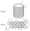
- FIG. 3A is a perspective view showing an example of the configuration of the master
- FIG. 3B is an enlarged plan view showing a part of the master shown in FIG. 3A.
- FIG. 4 is a schematic view showing an example of the configuration of an exposure apparatus for producing a master.
- FIG. 4 is a schematic view showing an example of the configuration of an exposure apparatus for producing a master.
- FIG. 5 is a schematic view showing an example of the configuration of an etching apparatus for producing a master.
- FIGS. 6A to 6C are process diagrams for explaining a method of manufacturing an optical element according to the first embodiment of the present invention.
- FIGS. 7A to 7C are process diagrams for explaining the method of manufacturing an optical element according to the first embodiment of the present invention.
- FIG. 8 is a schematic view showing an example of the configuration of an exposure apparatus used for manufacturing an optical element according to the second embodiment of the present invention.
- FIG. 9 is a schematic view showing an example of the configuration of an exposure apparatus used for manufacturing an optical element according to the second embodiment of the present invention.
- FIG. 10A is a schematic plan view showing an example of the configuration of an optical element according to the fourth embodiment of the present invention.
- FIG. 10B is an enlarged plan view showing a part of the optical element shown in FIG. 10A.
- FIG. 10C is a sectional view taken along tracks T1, T3,...
- FIG. 10D is a sectional view taken along tracks T2, T4,...
- FIG. 11A is a schematic plan view showing an example of the configuration of an optical element according to the fifth embodiment of the present invention.
- FIG. 11B is an enlarged plan view showing a part of the optical element shown in FIG. 12A.
- FIG. 11C is a sectional view taken along tracks T1, T3,... Of FIG.
- FIG. 11D is a sectional view taken along tracks T2, T4,...
- FIG. 12A is a side view showing an example of the configuration of the master.
- FIG. 12A is a side view showing an example of the configuration of the master.
- FIG. 12B is an enlarged plan view showing a part of the master shown in FIG. 12A.
- FIG. 13 is a schematic view showing an example of the configuration of an exposure apparatus for producing a master.
- FIG. 14 is a schematic view showing an example of the configuration of an etching apparatus for producing a master.
- FIG. 15A is a schematic plan view showing an example of the configuration of an optical element according to the sixth embodiment of the present invention.
- FIG. 15B is an enlarged plan view showing a part of the optical element shown in FIG. 15A.
- FIG. 15C is a sectional view taken along tracks T1, T3,... Of FIG.
- FIG. 15D is a sectional view taken along tracks T2, T4,... Of FIG.
- FIG. 16 is an enlarged perspective view showing a part of the optical element shown in FIG. FIG.
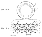
- FIG. 17A is a plan view showing an example of the configuration of the master.
- FIG. 17B is an enlarged plan view showing a part of the master shown in FIG. 17A.
- FIG. 18 is a schematic view showing an example of the configuration of an exposure apparatus for producing a master.
- FIG. 19 is a schematic view showing an example of the configuration of an etching apparatus for producing a master.
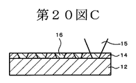
- FIGS. 20A to 20C are process diagrams for explaining a method of manufacturing an optical element according to the sixth embodiment of the present invention.
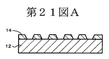
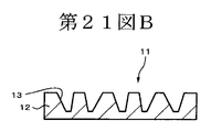
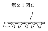
- 21A to 21C are process diagrams for explaining a method for manufacturing an optical element according to the sixth embodiment of the present invention.
- FIG. 22A is a schematic plan view showing an example of the configuration of an optical element according to the seventh embodiment of the present invention.
- FIG. 22B is an enlarged plan view showing a part of the optical element shown in FIG. 22A.
- 22C is a cross-sectional view taken along tracks T1, T3,...
- FIG. 22D is a sectional view taken along tracks T2, T4,...
- FIG. 23 is an enlarged perspective view showing a part of the optical element shown in FIG.
- FIG. 24 is a sectional view showing an example of the configuration of the liquid crystal display device according to the ninth embodiment of the present invention.
- FIG. 25 is a sectional view showing an example of the structure of the liquid crystal display device according to the tenth embodiment of the present invention.
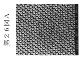
- FIG. 26A is a SEM photograph of the optical element of Example 1.
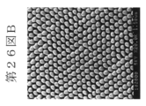
- FIG. 26B is a SEM photograph of the optical element of Example 2.
- FIG. 26A is a SEM photograph of the optical element of Example 1.
- FIG. 26B is a SEM photograph of the optical element of Example 2.
- FIG. 26A is a SEM photograph of the optical element of Example 1.
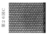
- FIG. 26C is a SEM photograph of the optical element of Example 3.
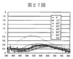
- FIG. 27 is a graph showing the antireflection characteristics of Example 1.
- FIG. 28A is a perspective view showing an appearance of a moth-eye lens film of Example 4.
- FIG. 28B is a sectional view taken along line AA in FIG. 28A.
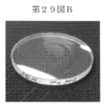
- FIGS. 29A and 29B are photographs showing the appearance of the moth-eye quartz lens of Example 5.
- FIG. 1A is a schematic plan view showing an example of the configuration of an optical element according to the first embodiment of the present invention.
- FIG. 1B is an enlarged plan view showing a part of the optical element shown in FIG. 1A.
- 1C is a cross-sectional view taken along tracks T1, T3,... Of FIG.
- FIG. 1D is a cross-sectional view taken along tracks T2, T4,...
- the optical element 1 is suitable for application to various optical components such as a display, optoelectronics, optical communication (optical fiber), solar cell, and lighting device.
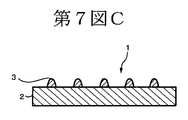
- the optical element 1 includes a base 2 and a structure 3 that is a convex portion formed on the surface of the base 2.
- the optical element 1 has a function of preventing reflection of light incident on the surface of the substrate on which the structure 3 is provided.
- X axis and Y axis two axes orthogonal to each other in one main surface of the base 2 are referred to as X axis and Y axis, and an axis perpendicular to one main surface of the base 2 is referred to as Z axis.
- the substrate 2 is a transparent substrate having transparency.
- the material of the base 2 include transparent synthetic resins such as polycarbonate (PC) and polyethylene terephthalate (PET), and materials mainly composed of glass, but are not particularly limited to these materials.
- the shape of the substrate 2 include a film shape, a sheet shape, a plate shape, and a block shape, but are not particularly limited to these shapes.
- the shape of the base 2 is a main body portion of various optical devices that require a predetermined antireflection function such as a display, optoelectronics, optical communication, a solar cell, and a lighting device, and a sheet or film attached to these optical devices. It is preferable to select and decide according to the shape of the antireflection functional component.
- FIG. 2 is an enlarged perspective view showing a part of the optical element shown in FIG. A large number of structures 3 that are convex portions are arranged on the surface of the base 2.
- the structures 3 are periodically two-dimensionally arranged at a short pitch equal to or less than the wavelength of light under the usage environment, for example, at a pitch comparable to the wavelength of visible light.
- the light under the usage environment is, for example, ultraviolet light, visible light, or infrared light.
- ultraviolet light means light having a wavelength range of 10 nm or more and less than 360 nm
- visible light means light of 360 nm or more and 830 nm or less
- infrared light means light of more than 830 nm and 1 mm or less.
- the structure 3 of the optical element 1 has an arrangement form that forms a plurality of rows of tracks T1, T2, T3,... (Hereinafter collectively referred to as “tracks T”) on the surface of the base 2.
- the track refers to a portion where the structures 3 are arranged in a straight line in a row.
- the lower portions of the adjacent structures 3 may be overlapped to join the lower portions of the structures 3 together.
- the bonding of the structures 3 is performed by all or part of the structures 3 that are adjacent to each other.
- the lower portions of the structures 3 arranged in the track direction are overlapped and joined.
- the structure 3 is disposed at a position shifted by a half pitch between two adjacent tracks T.
- the structure of the other track for example, T2
- the intermediate position position shifted by a half pitch
- a hexagonal lattice pattern or a quasi-hexagonal lattice pattern in which the center of the structure 3 is located at each point a1 to a7 between adjacent three rows of tracks (T1 to T3) is formed.
- the structure 3 is arranged.
- the hexagonal lattice pattern means a regular hexagonal lattice pattern.
- the quasi-hexagonal lattice pattern is a distorted hexagonal lattice pattern that is stretched in the track extending direction (X-axis direction), unlike a regular hexagonal lattice pattern.
- the distance is the arrangement pitch of the structures 3 between two adjacent tracks (for example, T1 and T2), that is, the arrangement pitch P2 of the structures 3 in the ⁇ ⁇ directions (for example, a1 to a7,. It is preferable that the distance is longer than (distance between a2 to a7).
- the height of the structure 3 is not particularly limited, and is appropriately set according to the wavelength region of light to be transmitted.
- the height of the structure 3 is, for example, 236 nm to 450 nm, preferably 415 nm to 421 nm.
- the aspect ratio (height H / arrangement pitch P) of the structures 3 is preferably set in the range of 0.81 to 1.46. If it is less than 0.81, the reflection characteristics and the transmission characteristics tend to be reduced, and if it exceeds 1.46, the peeling characteristics are lowered during the production of the optical element 1, and the replica tends to be unrecoverable. It is.
- the aspect ratio is defined by the following formula (1).
- Aspect ratio H / P (1)
- H Height of the structure 3
- P Average arrangement pitch (average period)
- the average arrangement pitch P is defined by the following equation (2).
- Average arrangement pitch P (P1 + P2 + P2) / 3 (2)
- P1 arrangement pitch in the track extending direction (track extending direction period)
- the height H of the structures 3 is the height H2 of the structures 3 in the column direction (see FIG. 2).
- the column direction means a direction (Y-axis direction) orthogonal to the track extending direction (X-axis direction) in the substrate surface.
- the height H1 in the track extending direction of the structure 3 is smaller than the height H2 in the column direction.
- the height of the structure 3 in a portion other than the track extending direction is substantially the same as the height H2 in the column direction.
- the height H of the structures 3 is represented by the height H2 in the column direction.
- the structures 3 have the same shape, but the shape of the structure 3 is not limited to this, and two or more types of structures 3 are formed on the surface of the substrate. May be.
- the structure 3 may be formed integrally with the base 2.
- the aspect ratios of the structures 3 are not limited to the same, and the structures 3 are configured to have a certain height distribution (for example, an aspect ratio in the range of about 0.83 to 1.46). Also good.
- the height distribution means that the structures 3 having two or more heights (depths) are provided on the surface of the base 2. That is, it means that the structure 3 having a reference height and the structure 3 having a height different from the structure 3 are provided on the surface of the base 2.
- the structures 3 having a height different from the reference are provided, for example, on the surface of the base 2 periodically or non-periodically (randomly).
- the material of the structure 3 is preferably, for example, an ionizing radiation curable resin that is cured by ultraviolet rays or electron beams, or a thermosetting resin that is cured by heat, and an ultraviolet curable resin that can be cured by ultraviolet rays.
- the main component is most preferable.
- the structure 3 preferably has a curved surface that gradually spreads from the top to the bottom of the structure 3. This is because transferability can be improved by using such a shape.
- the top of the structure 3 is, for example, a flat surface or a convex curved surface, preferably a convex curved surface.
- a low refractive index layer having a lower refractive index than that of the structure 3 may be formed on the top of the structure 3, and by forming such a low refractive index layer, the reflectance can be lowered.
- the overall shape of the structure 3 include a cone shape.
- the cone shape include a cone shape, a truncated cone shape, an elliptical cone shape, an elliptical truncated cone shape, a cone shape having a curvature at the top portion, and an elliptic cone shape having a curvature at the top portion.
- the cone shape includes an elliptical cone shape, an elliptical truncated cone shape, a cone shape with a curvature at the top, and an elliptic cone shape with a curvature at the top. It is a concept that includes. Further, the truncated cone shape refers to a shape obtained by cutting off the top portion of the truncated cone shape, and the elliptical truncated cone shape refers to a shape obtained by cutting off the top portion of the elliptical cone. Note that the overall shape of the structure 3 is not limited to these shapes, and can be appropriately selected according to desired characteristics.
- the structure 3 having an elliptical cone shape is an elliptical, oval or egg-shaped cone structure having a bottom surface having a major axis and a minor axis, and a top portion having a curved surface.
- the structure 3 having an elliptical truncated cone shape is an elliptical, oval or egg-shaped pyramid structure with a bottom surface having a major axis and a minor axis, and a top portion is flat.
- the structure 3 is formed on the substrate surface so that the major axis direction of the bottom surface of the structure 3 is the track extending direction (X-axis direction).
- FIG. 3 shows an example of the configuration of a master for producing an optical element having the above-described configuration.
- the master 11 is a so-called roll master, and has a structure in which a large number of structures 13 that are concave portions are arranged on the surface of a cylindrical master 12.
- the structures 13 are periodically two-dimensionally arranged at a pitch equal to or less than the wavelength of light in the environment in which the optical element 1 is used, for example, the wavelength of visible light.
- the structure 13 is arranged concentrically or spirally on the surface of the columnar master 12.
- the structure 13 is for forming the structure 3 that is a convex portion on the surface of the base 2 described above.
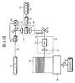
- FIG. 4 is a schematic view showing an example of the configuration of an exposure apparatus for producing a master having the above-described configuration.
- This exposure apparatus is configured based on an optical disk recording apparatus.
- the laser light 15 emitted from the laser light source 21 travels straight as a parallel beam and enters an electro-optic element (EOM: Electro Optical Modulator) 22.
- EOM Electro Optical Modulator
- the laser beam 15 transmitted through the electro-optical element 22 is reflected by the mirror 23 and guided to the modulation optical system 25.
- the mirror 23 is composed of a polarization beam splitter and has a function of reflecting one polarization component and transmitting the other polarization component.
- the polarized light component transmitted through the mirror 23 is received by the photodiode 24, and the electro-optic element 22 is controlled based on the received light signal, and the phase modulation of the laser light 15 is performed.
- the laser beam 15 is transmitted through a condenser lens 26 to glass (SiO 2). 2 ) Or the like, the light is condensed on an AOM (Acoustic-Optic Modulator) 27.
- AOM Acoustic-Optic Modulator
- the laser beam 15 is intensity-modulated by the acousto-optic element 27 and diverges, and then converted into a parallel beam by the collimator lens 28.
- the laser beam 15 emitted from the modulation optical system 25 is reflected by the mirror 31 and guided horizontally and in parallel on the moving optical table 32.
- the moving optical table 32 includes a beam expander 33 and an objective lens 34.
- the laser light 15 guided to the moving optical table 32 is shaped into a desired beam shape by the beam expander 33 and then irradiated to the resist layer on the master 12 through the objective lens 34.
- the master 12 is placed on a turntable 36 connected to a spindle motor 35.
- the resist layer is exposed by intermittently irradiating the resist layer with the laser beam 15 while rotating the master 12 and moving the laser beam 15 in the height direction of the master 12.
- the formed latent image has, for example, a substantially elliptical shape having a major axis in the circumferential direction.
- the laser beam 15 is moved by moving the moving optical table 32 in the arrow R direction.
- the exposure apparatus includes a control mechanism 37 for forming a latent image corresponding to the two-dimensional pattern of the hexagonal lattice or the quasi-hexagonal lattice shown in FIG. 1B on the resist layer.
- the control mechanism 37 includes a formatter 29 and a driver 30.
- the formatter 29 includes a polarity reversal unit, and this polarity reversal unit controls the irradiation timing of the laser beam 15 on the resist layer.
- the driver 30 receives the output from the polarity inversion unit and controls the acoustooptic device 27.
- a signal is generated by synchronizing the polarity inversion formatter signal and the rotation controller of the recording apparatus for each track so that the two-dimensional pattern is spatially linked, and the intensity is modulated by the acoustooptic device 27. .
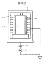
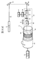
- FIG. 5 is a schematic view showing an example of the configuration of an etching apparatus for producing a master having the above-described configuration.
- the etching apparatus is a so-called RIE (Reactive Ion Etching) apparatus.
- RIE Reactive Ion Etching
- the cylindrical electrode 42 is disposed in the center of the etching reaction tank 41.
- a counter electrode 43 is provided inside the etching reaction tank 41.
- the columnar electrode 42 has a configuration in which the cylindrical master 12 can be attached and detached.
- the columnar electrode 42 has, for example, a columnar surface that is substantially the same or similar to the cylindrical surface of the cylindrical master 12, specifically, a columnar surface having a slightly smaller diameter than the inner peripheral surface of the cylindrical master 12.
- the cylindrical electrode 43 is connected to a high frequency power supply (RF) 45 of 13.56 MHz, for example, via a blocking capacitor 44.
- the counter electrode 43 is connected to the ground.
- etching apparatus having the above-described configuration, when a high frequency voltage is applied between the counter electrode 43 and the cylindrical electrode 42 by the high frequency power supply 45, plasma is generated between the counter electrode 43 and the cylindrical electrode 42. Since the counter electrode 43 is connected to the ground, the potential does not change. On the other hand, the cylindrical electrode 42 has a negative potential because the circuit is blocked by the blocking capacitor 44, and a voltage drop occurs. Due to this voltage drop, an electric field is generated in a direction perpendicular to the cylindrical surface of the cylindrical electrode 42, and positive ions in the plasma are incident perpendicularly to the outer peripheral surface of the cylindrical master 12 and anisotropic etching is performed.
- the method for manufacturing an optical element according to the first embodiment is a method in which an optical disc master production process and an etching process are combined.
- the manufacturing method includes a resist film forming step for forming a resist layer on the master, an exposure step for forming a latent image on the resist layer using an exposure apparatus, a developing step for developing the resist layer on which the latent image is formed, An etching process for manufacturing a master by etching and a replication process for manufacturing a replication substrate by an ultraviolet curable resin are provided.
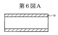
- a cylindrical master 12 is prepared.
- the master 12 is, for example, a glass master.
- an inorganic resist layer 14 is formed on the outer peripheral surface of the cylindrical master 12 by sputtering.
- the inorganic resist for example, a metal oxide made of one or more transition metals such as tungsten and molybdenum can be used.
- the master 12 is rotated and the laser beam (exposure beam) 15 is irradiated to the inorganic resist layer 14 using the exposure apparatus shown in FIG.
- the inorganic resist layer 14 is exposed over the entire surface by intermittently irradiating the laser beam 15 while moving the laser beam 15 in the height direction of the master 12.
- the latent image 16 according to the locus of the laser beam 15 is formed over the entire surface of the inorganic resist layer 14 at a pitch similar to the visible light wavelength, for example.
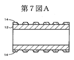
- a developer is dropped on the inorganic resist layer 14 to develop the inorganic resist layer 14 as shown in FIG. 7A.
- the exposed portion exposed with the laser beam 15 has a higher dissolution rate with respect to the developer than the non-exposed portion. Therefore, as shown in FIG. 7A.
- a pattern corresponding to the latent image (exposed portion) 16 is formed on the inorganic resist layer 14. (Etching process)
- the surface of the master 12 is etched using the pattern (resist pattern) of the inorganic resist layer 14 formed on the master 12 as a mask. Thereby, as shown in FIG.
- the structure 13 for example, an elliptical cone-shaped or elliptical truncated cone-shaped recess having the major axis direction in the track extending direction, that is, the structure 13 can be obtained. Moreover, you may make it perform an etching process and an ashing process alternately as needed. By doing in this way, the structure 13 which has a various curved surface can be formed. For example, by alternately repeating ashing and etching, and gradually increasing the etching time, the shape of the structure 3 can be changed to an elliptical cone having a gentle slope at the top and a gradually steep slope from the center to the bottom. Can be shaped.
- a glass master having a depth three times or more of the inorganic resist layer 14 (selection ratio 3 or more) can be produced, and the structure 3 can have a high aspect ratio.
- the master 11 having a hexagonal lattice pattern or a quasi-hexagonal lattice pattern is obtained.
- the master 11 and the substrate 2 such as an acrylic sheet coated with an ultraviolet curable resin are brought into close contact with each other, irradiated with ultraviolet rays to cure the ultraviolet curable resin, and then the substrate 2 is peeled from the master 11. Thereby, as shown in FIG. 7C, the target optical element 1 is manufactured.
- the inorganic resist layer 14 is formed by the sputtering method, a smooth inorganic resist film having a uniform film thickness can be formed on the surface of the cylindrical master 12.
- the cylindrical master 12 is disposed on the column electrode 42 and reactive ion etching is performed, positive ions can be incident on the outer peripheral surface of the cylindrical master 12 perpendicularly to perform anisotropic etching.
- an uneven pattern having a uniform depth and width can be formed on the master 12 having a cylindrical surface.
- the optical element 1 is manufactured by using a method in which an optical disk master production process and an etching process are combined, the master disk production process is performed as compared with the case where the optical element 1 is produced using electron beam exposure.
- the time required (exposure time) can be greatly reduced. Therefore, the productivity of the optical element 1 can be greatly improved. Further, when the shape of the top of the structure 3 is not sharp but smooth, for example, a smooth curved surface protruding in the height direction, the durability of the optical element 1 can be improved. Moreover, the peelability of the optical element 1 with respect to the master 11 can also be improved.
- the process of forming an organic resist film by a general spin coating method when the master has a curved surface (cylindrical or spherical), uneven coating occurs, and it is difficult to form a smooth resist film with a uniform film thickness. It is. Therefore, it is difficult to form an uneven pattern having a uniform depth and width on the curved master surface.
- the inorganic resist layer 14 is formed by sputtering, a smooth inorganic resist film having a uniform film thickness can be formed on the surface of the cylindrical master 12. Therefore, an uneven pattern having a uniform depth and width can be formed on the curved master surface. Further, by applying the above-described manufacturing method, it is possible to form a concavo-convex pattern having a uniform depth and width in addition to a master having a curved surface such as a cylinder or a sphere. For example, an uneven pattern having a uniform depth and width can be formed on a master such as a sheet, tape, bar, needle, rectangular parallelepiped (box), wire frame, or cylinder.
- a master such as a sheet, tape, bar, needle, rectangular parallelepiped (box), wire frame, or cylinder.
- FIG. 8 is a schematic view showing an example of the configuration of an exposure apparatus used for manufacturing an optical element according to the second embodiment of the present invention. As shown in FIG. 8, the second embodiment is different from the first embodiment in that exposure is performed with a cylindrical master 12 lying sideways.
- This exposure apparatus includes a turntable 60, a spindle servo 61, a laser light source 51 (266 nm), a mirror M1 and a mirror M2, a drive circuit (driver) 58, a moving optical table 53, a voltage frequency controller 57, an air slider (not shown). ), A feed servo (not shown), and a focus servo (not shown) of a defocusing method (skew method) are provided as main parts.
- the light source for exposure is not limited to such a laser light source 51 in particular.
- the laser light 52 emitted from the laser light source 51 travels straight as a parallel beam, is reflected by the mirror M1 and the mirror M2, changes its direction, and is guided to the moving optical table 53.
- two wedge prisms 54 and one acousto-optic modulation deflector (AOM / AOD; Acoustic Optical Modulator / Acoustic Optical Defector) 55 are arranged on the moving optical table 53.
- the wedge prism 54 and the acousto-optic modulation deflector 55 are arranged so that the laser beam 52 and the grating surface incident as parallel beams satisfy the Bragg condition and the beam horizontal height does not change.
- quartz (SiO 2 ) As an acoustooptic device used for the acoustooptic modulation deflector 55, quartz (SiO 2 ) Is preferred.
- a predetermined signal is supplied from the drive circuit 58 to the acousto-optic modulation deflector 55.
- the drive circuit 58 is supplied with a high frequency signal from a voltage frequency controller (VCO) 57.
- a control signal is supplied to the voltage frequency controller 57.
- the acousto-optic modulation deflector 55 utilizes the fact that the first-order diffracted light intensity in Bragg diffraction is substantially proportional to the ultrasonic power, and modulates the ultrasonic power based on the recording signal to modulate the laser light 52. And a predetermined exposure pattern is formed.
- the positional relationship and attitude of the acousto-optic modulation deflector 55 with respect to the optical axis of the laser beam 52 are set.
- FIG. 9 is a schematic view showing an example of the configuration of an exposure apparatus used for manufacturing an optical element according to the second embodiment of the present invention. As shown in FIG.
- FIG. 10A is a schematic plan view showing an example of the configuration of an optical element according to the fourth embodiment of the present invention.
- FIG. 10B is an enlarged plan view showing a part of the optical element shown in FIG. 10A.
- FIG. 10C is a sectional view taken along tracks T1, T3,...
- FIG. 10D is a sectional view taken along tracks T2, T4,... Of FIG.
- the optical element 1 according to the fourth embodiment is different from that of the first embodiment in that the structure 3 forms a tetragonal lattice pattern or a quasi-tetragonal lattice pattern between adjacent three rows of tracks. ing.
- the quasi-tetragonal lattice pattern means a distorted tetragonal lattice pattern that is stretched in the track extending direction (X-axis direction).
- the structures 3 are periodically arranged in a tetragonal lattice pattern or a quasi-tetragonal lattice pattern, for example, the structures 3 are adjacent to each other in an orientation that is four-fold symmetric.
- the structure 3 of the other track (for example, T2) is arranged at an intermediate position (position shifted by a half pitch) of the structures 3 arranged on one track (for example, T1). Yes. As a result, as shown in FIG.
- a tetragonal lattice pattern or a quasi-tetragonal lattice pattern in which the center of the structure 3 is located at each point a1 to a4 between adjacent three rows of tracks (T1 to T3) is formed.
- the structure 3 is arranged.
- the height (depth) of the structure 3 is not particularly limited, and is appropriately set according to the wavelength region of light to be transmitted. For example, when visible light is transmitted, the height (depth) of the structure 3 is preferably 150 nm to 500 nm.
- the pitch P2 in the ⁇ direction with respect to the track T is, for example, about 275 nm to 297 nm.
- the aspect ratio (height H / arrangement pitch P) of the structures 3 is, for example, about 0.54 to 1.13. Furthermore, the aspect ratios of the structures 3 are not limited to the same, and the structures 3 may be configured to have a certain height distribution.
- the arrangement pitch P1 of the structures 3 in the same track is preferably longer than the arrangement pitch P2 of the structures 3 between two adjacent tracks.
- the ratio P1 / P2 is 1.4 ⁇ P1 / P2 ⁇ 1. It is preferable that the relationship 5 is satisfied.
- FIG. 11A is a schematic plan view showing an example of the configuration of an optical element according to the fifth embodiment of the present invention.
- FIG. 11B is an enlarged plan view showing a part of the optical element shown in FIG. 12A.
- FIG. 11C is a sectional view taken along tracks T1, T3,... Of FIG. FIG.
- FIG. 11D is a sectional view taken along tracks T2, T4,...
- the optical element 1 according to the fifth embodiment is different from the first embodiment in that the optical element 1 has a spherical surface and the structure 3 is formed on the spherical surface.
- the spherical surface is, for example, a convex or concave spherical surface.
- the optical element 1 is, for example, a concave lens or a convex lens.
- FIG. 11 shows an example in which the optical element 1 has a concave spherical surface.
- the optical element 1 according to the fifth embodiment is the same as the first embodiment except for the above.
- FIG. 12 shows an example of the configuration of a master for producing an optical element having the above-described configuration.
- the master 11 according to the fifth embodiment is different from the first embodiment in that it has a spherical surface and the structure 13 is formed on the spherical surface.
- the spherical surface is, for example, a convex or concave spherical surface.
- FIG. 12 the case where the master 11 has a convex spherical surface is shown as an example.
- the master 11 according to the fifth embodiment is the same as the first embodiment except for the above.
- FIG. 13 is a schematic view showing an example of the configuration of an exposure apparatus for producing a master having the above-described configuration.
- the moving optical table 32 includes a beam expander 33, a mirror 38, and an objective lens 34.
- a position sensor (not shown) is provided at a position directly below the objective lens 34. By this position sensor, collision with the spherical surface of the master 12 is prevented.
- the laser beam 15 guided to the moving optical table 32 is shaped into a desired beam shape by the beam expander 33, and then passes through the mirror 38 and the objective lens 34 to the resist layer formed on the spherical surface of the master 12. Irradiated.
- the master 12 having a spherical surface is placed on a turntable 36 connected to a spindle motor 35. Then, while rotating the master 12 and moving the laser beam 15 in the rotational radius direction of the master 12, the resist layer on the master 12 is intermittently irradiated with the laser beam, whereby the resist layer exposure process is performed. .
- FIG. 14 is a schematic view showing an example of the configuration of an etching apparatus for producing a master having the above-described configuration.
- a spherical electrode 46 and a counter electrode 47 facing the spherical electrode 46 are provided in the etching reaction tank 41.
- the spherical electrode 46 has a spherical surface on the side facing the counter electrode 47, and the master 12 is placed on this spherical surface.
- the spherical electrode 46 is configured so that the spherical master 12 can be attached and detached.
- FIG. 15A is a schematic plan view showing an example of the configuration of an optical element according to the sixth embodiment of the present invention.
- FIG. 15B is an enlarged plan view showing a part of the optical element shown in FIG. 15A.
- FIG. 15C is a sectional view taken along tracks T1, T3,... Of FIG.
- FIG. 15D is a sectional view taken along tracks T2, T4,... Of FIG. FIG.
- FIG. 16 is an enlarged perspective view showing a part of the optical element shown in FIG.
- the sixth embodiment is different from the first embodiment in that the structure 3 is inclined with respect to the substrate surface.
- the structure 3 may face two or more different directions with respect to the substrate surface.
- the structure 3 may be formed obliquely in two or more different directions with a predetermined angle with respect to the normal direction of the substrate surface, for example.
- the structure 3 may have a plurality of regions, and the direction of the structure may be different depending on each region.
- the optical element according to the sixth embodiment is the same as the first embodiment except for the above.
- FIG. 17 shows an example of the configuration of a master for producing an optical element having the above-described configuration. As shown in FIG.
- the master 11 has a structure in which a large number of structures 13 that are concave portions are arranged on the surface of a disk-shaped master 12.
- the structures 13 are periodically two-dimensionally arranged at a pitch equal to or less than the wavelength of light in the environment in which the optical element 1 is used, for example, the wavelength of visible light.
- the structure 13 is disposed on, for example, a concentric or spiral track.
- the master according to the sixth embodiment is the same as the first embodiment except for the above.
- FIG. 18 is a schematic view showing an example of the configuration of an exposure apparatus for producing a master having the above-described configuration.
- the exposure apparatus according to the sixth embodiment is the same as that of the fifth embodiment. However, in the sixth embodiment, as shown in FIG.
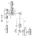
- FIG. 19 is a schematic view showing an example of the configuration of an etching apparatus for producing a master having the above-described configuration.
- an uneven surface electrode 48 and a counter electrode 47 facing the uneven surface electrode 48 are provided in the etching reaction tank 41.
- the uneven surface electrode 48 has an uneven surface on the side facing the counter electrode 47, and the master 12 is placed on the uneven surface.
- the master 12 can be anisotropically etched in two or more different directions using the concavo-convex surface of the concavo-convex surface electrode 48.
- the concavo-convex shape of the concavo-convex surface electrode 48 it is possible to change the direction of anisotropic etching according to the surface area of the master 12 using the concavo-convex surface of the concavo-convex surface electrode 48. is there.
- the etching apparatus according to the sixth embodiment is the same as the first embodiment except for the above.
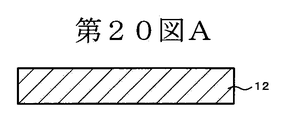
- FIG. 20A a disk-shaped master 12 is prepared.
- the master 12 is, for example, a glass master.
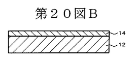
- an inorganic resist layer 14 is formed on one main surface of the disk-shaped master 12 by a sputtering method.
- the inorganic resist for example, a metal oxide made of one or more transition metals such as tungsten and molybdenum can be used.
- the master 12 is rotated and the inorganic resist layer 14 is irradiated with a laser beam (exposure beam) 15 using the exposure apparatus shown in FIG.
- the inorganic resist layer 14 is exposed over the entire surface by intermittently irradiating the laser beam 15 while moving the laser beam 15 in the height direction of the master 12.
- the latent image 16 according to the locus of the laser beam 15 is formed over the entire surface of the inorganic resist layer 14 at a pitch similar to the visible light wavelength, for example.
- a developer is dropped on the inorganic resist layer 14 to develop the inorganic resist layer 14 as shown in FIG. 21A.
- the exposed portion exposed with the laser beam 15 has a higher dissolution rate with respect to the developer than the non-exposed portion. Therefore, as shown in FIG. 21A.
- a pattern corresponding to the latent image (exposed portion) 16 is formed on the inorganic resist layer 14.
- the surface of the master 12 is etched using the pattern (resist pattern) of the inorganic resist layer 14 formed on the master 12 as a mask.
- a structure 13 is formed that is directed in various directions such as an oblique direction with respect to one main surface of the disk-shaped master 12.
- the structure 13 which has a various curved surface can be formed.
- the master 11 in which the structure 3 is formed in an oblique direction with respect to the substrate surface is obtained.
- the master 11 and the substrate 2 such as an acrylic sheet coated with an ultraviolet curable resin are brought into close contact with each other, irradiated with ultraviolet rays to cure the ultraviolet curable resin, and then the substrate 2 is peeled from the master 11.
- the target optical element 1 is manufactured.
- FIG. 22A is a schematic plan view showing an example of the configuration of an optical element according to the seventh embodiment of the present invention.
- FIG. 22B is an enlarged plan view showing a part of the optical element shown in FIG. 22A.
- 19C is a cross-sectional view taken along tracks T1, T3,... Of FIG. 22D is a cross-sectional view taken along tracks T2, T4,... Of FIG.
- FIG. 23 is an enlarged perspective view showing a part of the optical element shown in FIG.
- the optical element 1 according to the seventh embodiment is different from that of the first embodiment in that a large number of structures 3 that are concave portions are arranged on the surface of the substrate.
- the shape of the structure 3 is a concave shape obtained by inverting the convex shape of the structure 3 in the first embodiment.
- the eighth embodiment is different from the first embodiment in that an inorganic resist layer 14 is developed to form a concavo-convex pattern and is directly used as a master.
- an optical element is produced as follows. First, the steps from the resist film formation step to the development step are performed in the same manner as in the first embodiment. Thereby, concave portions of a hexagonal lattice pattern or a quasi-hexagonal lattice pattern are formed in the inorganic resist layer 14. Next, the optical element 1 is manufactured as follows using the master 12 having such a pattern formed on the inorganic resist layer 14 as a master.
- the eighth embodiment is the same as the first embodiment except for the above.
- a highly rigid inorganic resist layer 14 is formed on a master 12 such as a metal master or sheet by sputtering, and the inorganic resist layer 14 is exposed and developed to form an inorganic material.
- An uneven pattern is formed on the resist layer 14. Therefore, the master 12 having the uneven pattern of the inorganic resist layer 14 can be used directly as a stamper.
- FIG. 24 shows an example of the configuration of the liquid crystal display device according to the ninth embodiment of the present invention. As shown in FIG.
- this liquid crystal display device includes a backlight 73 that emits light, and a liquid crystal panel 71 that temporally and spatially modulates the light emitted from the backlight 73 to display an image.
- Polarizers 71a and 71b are provided on both surfaces of the liquid crystal panel 71, respectively.
- the optical element 1 is provided on the polarizer 71 b provided on the display surface side of the liquid crystal panel 71.
- the polarizer 71b in which the optical element 1 is provided on one main surface is referred to as a polarizer 72 with an antireflection function.
- This polarizer 72 with an antireflection function is an example of an optical component with an antireflection function.
- the backlight 73 for example, a direct backlight, an edge backlight, or a flat light source backlight can be used.
- the backlight 73 includes, for example, a light source, a reflecting plate, an optical film, and the like.
- the light source include a cold cathode fluorescent lamp (CCFL), a hot cathode fluorescent lamp (HCFL), an organic electroluminescence (OEL), an inorganic electroluminescence (OEL), and an inorganic electroluminescence (OEL).
- liquid crystal panel 71 for example, a twisted nematic (TN) mode, a super twisted nematic (STN) mode, a vertical alignment (Vertical Aligned: VA) mode, a horizontal alignment (In-Plane: Switch) is used.
- TN twisted nematic
- STN super twisted nematic
- VA vertical alignment
- VA horizontal alignment
- In-Plane: Switch horizontal alignment
- Mode optically compensated bend alignment
- CGH light emitting diode
- polarizers 71a and 71b are provided on both surfaces of the liquid crystal panel 71 so that their transmission axes are orthogonal to each other.
- the polarizers 71a and 71b allow only one of the orthogonal polarization components of incident light to pass through and shield the other by absorption.
- the polarizers 71a and 71b include hydrophilic polymer films such as polyvinyl alcohol films, partially formalized polyvinyl alcohol films, ethylene / vinyl acetate copolymer partially saponified films, iodine, dichroic dyes, and the like. Those obtained by adsorbing the dichroic substance and uniaxially stretching can be used.
- the protective layer is provided in this way, it is preferable that the base 2 of the optical element 1 also serves as the protective layer. This is because the polarizer 72 with an antireflection function can be thinned by adopting such a configuration.
- TAC triacetyl cellulose Since the optical element 1 is the same as any one of the first to fourth, sixth, and seventh embodiments described above, the description thereof is omitted. According to the ninth embodiment, since the optical element 1 is provided on the display surface of the liquid crystal display device, the antireflection function of the display surface of the liquid crystal display device can be improved.
- FIG. 25 shows an example of the configuration of the liquid crystal display device according to the tenth embodiment of the present invention.
- this liquid crystal display device includes a front member 74 on the front side of the liquid crystal panel 71, and the optical element 1 is provided on at least one of the front surface of the liquid crystal panel 71, the front surface and the back surface of the front member 74. Is different from that of the ninth embodiment.
- FIG. 25 shows an example in which the optical element 1 is provided on the front surface of the liquid crystal panel 71 and all the front and back surfaces of the front member 74.
- an air layer is formed between the liquid crystal panel 71 and the front member 74.
- the front surface refers to the surface on the side serving as the display surface, that is, the surface on the viewer side
- the back surface refers to the surface on the side opposite to the display surface.
- the front member 74 is a front panel or the like used for the purpose of mechanical, thermal, and weatherproof protection and design on the front surface (observer side) of the liquid crystal panel 71.
- the front member 74 has, for example, a sheet shape, a film shape, or a plate shape.
- Examples of the material of the front member 74 include glass, triacetyl cellulose (TAC), polyester (TPEE), polyethylene terephthalate (PET), polyimide (PI), polyamide (PA), aramid, polyethylene (PE), polyacrylate, Polyether sulfone, polysulfone, polypropylene (PP), diacetyl cellulose, polyvinyl chloride, acrylic resin (PMMA), polycarbonate (PC), and the like can be used, but the material is not particularly limited and is transparent. Any material having a property can be used. According to the tenth embodiment, the visibility of the liquid crystal display device can be improved as in the ninth embodiment.
- Example 1 First, an inorganic resist layer made of an oxide of tungsten (W) and molybdenum (Mo) was formed on a disk-shaped quartz substrate by a sputtering method. Next, a quasi-hexagonal lattice pattern latent image was formed on the inorganic resist layer using the exposure apparatus shown in FIG. Thereafter, the resist layer was subjected to development processing to produce a resist pattern. A 2.38% tetramethylammonium hydroxide aqueous solution (Tokyo Ohka Kogyo Co., Ltd.) was used as the developer.
- W tungsten
- Mo molybdenum
- Example 2 A duplicate substrate was obtained in the same manner as in Example 1 except that the uneven shape of the uneven electrode of the etching apparatus was changed.
- Example 3 First, a glass roll master having an outer diameter of 126 mm was prepared, and an inorganic resist layer made of an oxide of tungsten (W) and molybdenum (Mo) was formed on the surface of the glass roll master by a sputtering method.
- the glass roll master as a recording medium was conveyed to the exposure apparatus shown in FIG. 4 to expose the inorganic resist layer.
- a latent image forming a quasi-hexagonal lattice pattern between the adjacent three rows of tracks was patterned on the resist while continuing in one spiral shape.
- the inorganic resist layer on the glass roll master was subjected to development treatment, and the exposed portion of the resist was dissolved and developed.
- an undeveloped glass roll master is placed on a turntable of a developing machine (not shown), and a developer is dropped on the surface of the glass roll master while rotating the entire turntable to develop the resist on the surface. .
- a resist glass master having a resist layer opened in a quasi-hexagonal lattice pattern was obtained.
- the developer used was 2.38% tetramethylammonium hydroxide aqueous solution (Tokyo Ohka Kogyo Co., Ltd.).
- a process of etching the glass roll master by RIE etching and a process of removing the resist pattern by ashing and widening the opening diameter were repeated. Etching was performed using an etching apparatus having a cylindrical electrode shown in FIG.
- the quasi-hexagonal lattice pattern diameter at which the surface of the glass roll master is exposed gradually expands while etching proceeds in the direction perpendicular to the surface of the glass roll master, and the resist pattern is used as a mask in other areas. It was not etched. Thereby, the recessed part which goes to a perpendicular direction with respect to the surface of a glass roll original recording was formed. Finally, the resist pattern was completely removed by ashing. Thus, the intended glass roll master was obtained. Next, the produced glass roll master and an acrylic sheet coated with an ultraviolet curable resin were brought into close contact with each other, and peeled while being cured by irradiation with ultraviolet rays to produce an optical element.
- FIG. 26A and FIG. 26B show that the structure can be formed in an oblique direction with respect to the substrate by etching using the concavo-convex surface electrode. Moreover, it turns out that the direction of a structure can be changed according to an area
- FIG. 26C shows that a structure can be formed in a direction perpendicular to the substrate by etching using a cylindrical electrode. (Evaluation of reflectance) The reflectance of the optical element of Example 1 manufactured as described above was measured.
- FIG. 27 shows the following.
- Light having an incident angle of 30 degrees or 40 degrees tends to have a lower reflectance than light having an incident angle of 5 degrees. That is, in the optical element of Example 1, the effect of the antireflection characteristic is most remarkable for light having an incident angle of 30 degrees or 40 degrees. This is because in the optical element of Example 1, the structure is formed with an inclination of approximately 30 to 40 degrees with respect to the normal of the substrate. As described above, when the structure is formed to be inclined with respect to the normal of the substrate, angle dependency can be imparted to the antireflection characteristic of the optical element.
- Example 4 An optical element having such characteristics is effective when it is particularly desired to reduce the reflectance of light incident from a predetermined angle.
- a strip-like optical element was produced in the same manner as in Example 3.
- a predetermined rectangular optical element was cut out from the band-shaped optical element.
- this rectangular optical element was bent into a spherical shape with a hot water bath at a temperature of 80 ° C. to obtain a moth-eye lens film.
- FIGS. 28A and 28B show the appearance and cross section of the moth-eye lens film obtained as described above. (Evaluation of reflection characteristics) The reflectance of the moth-eye lens film of Example 4 produced as described above was measured.
- Example 5 First, a quartz lens (convex lens) having a spherical surface was prepared, and an inorganic resist layer made of an oxide of tungsten (W) and molybdenum (Mo) was formed on the spherical surface of the quartz lens as a master by sputtering. Next, the master as a recording medium was conveyed to the exposure apparatus shown in FIG.
- FIGS. 29A and 29B show the appearance of the moth-eye quartz lens obtained as described above. (Evaluation of reflection characteristics) The reflectance of the moth-eye quartz lens of Example 5 produced as described above was measured.
- the ultraviolet visible spectrophotometer (The JASCO Corporation make, brand name: V-550) was used for the measurement of a reflectance. From this evaluation result, it was found that the anti-reflection characteristic excellent in the moth-eye quartz lens of Example 5 was obtained.
- this invention is not limited to the above-mentioned embodiment, The various deformation
- the configurations, shapes, numerical values, and the like given in the above-described embodiments are merely examples, and different configurations, shapes, numerical values, and the like may be used as necessary.
- an inorganic resist is formed by sputtering on the surface of a box (cuboid), a wire frame, a cylinder, or the inside of a box, thereby forming a smooth resist film with a uniform film thickness.
- corrugated pattern can be formed by exposing an inorganic resist film with a stepper, recording various patterns, and developing.
- a smooth inorganic resist film with a uniform thickness is formed on an oval sphere (rugby ball type), conical shape, master plate with many holes, master plate with concave portions, master plate with convex portions, etc., and exposure development By doing so, it is also possible to form a desired uneven pattern.
- the present invention can also be applied to a substrate or device having a concavo-convex portion, a substrate having a wave surface or a curved surface, or the like used for a display or the like.
- a structure can be formed in an oblique direction or the like with respect to the surface of the cylindrical master and the spherical master.
- the electrodes of the optical element and the etching apparatus are a cylindrical surface and a spherical surface has been described as an example.
- the shapes of the electrodes of the optical element and the etching apparatus are not limited thereto. .
- curved surface shapes for example, various curved surfaces such as hyperboloids, free-form surfaces, and ellipsoids can be used.
- an optical element or the like is manufactured using an inorganic resist has been described.
- an organic resist can also be used.
Abstract
Description
一般に、光学素子表面に周期的な凹凸形状を設けた場合、ここを光が透過するときには回折が発生し、透過光の直進成分が大幅に減少する。しかし、凹凸形状のピッチが透過する光の波長よりも短い場合には回折は発生せず、例えば凹凸形状を矩形としたときに、そのピッチや深さなどに対応する単一波長の光に対して有効な反射防止効果を得ることができる。
本発明者らは、このような微細加工体の製造方法として、光ディスクの原盤作成プロセスとエッチングプロセスとを融合した方法を提案している(例えば特開2008−176076号公報参照)。この方法では、釣鐘形状や楕円錐台形状の構造体を形成することができる。
一般的な光ディスクの原盤作製プロセスでは、凹凸パターンは以下のようにして作製される。まず、感光材であるレジストをシンナーで希釈した溶液を、平滑なガラス基板上にスピンコート法により塗布することによって、均一な膜厚で平滑なレジスト膜を基板上に形成する。次に、基板のレジスト膜を光学記録装置により種々の露光パターンを記録し、現像する。ことにより、均一な深さや幅を有する凹凸パターンが形成される。 In recent years, various techniques for manufacturing finely processed bodies have been studied. For example, for the purpose of preventing light surface reflection, a technique for forming a fine and dense uneven structure (moth eye structure) on the surface of an optical element has been proposed (for example, “Optical Technology Contact” Vol. 43, No. 11 (2005). ), 630-637).
In general, when a periodic concavo-convex shape is provided on the surface of an optical element, diffraction occurs when light passes through the surface, and the linear component of transmitted light is greatly reduced. However, diffraction does not occur when the concave-convex pitch is shorter than the wavelength of the transmitted light. For example, when the concave-convex shape is rectangular, for a single wavelength light corresponding to the pitch, depth, etc. Effective antireflection effect can be obtained.
The inventors of the present invention have proposed a method that combines an optical disc mastering process and an etching process as a method of manufacturing such a finely processed body (see, for example, Japanese Patent Application Laid-Open No. 2008-176076). In this method, a bell-shaped or elliptic frustum-shaped structure can be formed.
In a general optical disk master production process, the concavo-convex pattern is produced as follows. First, a solution obtained by diluting a resist, which is a photosensitive material, with a thinner is applied onto a smooth glass substrate by a spin coating method to form a smooth resist film with a uniform film thickness on the substrate. Next, various exposure patterns are recorded and developed on the resist film of the substrate by an optical recording apparatus. Thus, a concavo-convex pattern having a uniform depth and width is formed.
したがって、この発明の目的は、球面や円柱面などの曲面上に微細な凹凸パターンを有する微細加工体、およびその製造方法、ならびにその作製に用いられるエッチング装置を提供することにある。 By the way, in recent years, for the purpose of preventing reflection and the like, it has been desired to form the above-described concavo-convex structure (moth eye structure) on various optical components. In order to meet such a requirement, a technique for forming a fine uneven pattern on a master having a curved surface such as a spherical surface or a cylindrical surface is required.
Accordingly, an object of the present invention is to provide a fine processed body having a fine uneven pattern on a curved surface such as a spherical surface or a cylindrical surface, a manufacturing method thereof, and an etching apparatus used for the manufacturing thereof.
曲面を有する原盤上に無機レジスト層を成膜する工程と、
原盤上に成膜された無機レジスト層を露光現像し、無機レジスト層にパターンを形成する工程と、
無機レジスト層にパターンが形成された原盤を、原盤の曲面とほぼ同一または相似の曲面を有する電極上に配置し、原盤をエッチングし、原盤表面に凹凸形状を形成することにより、微細加工体を作製する工程と
を備える微細加工体の製造方法である。
第2の発明は、
曲面を有する基体と、
基体の曲面上に形成された、凸部または凹部である構造体と
を備え、
構造体が、使用環境下の光の波長以下のピッチで配列されている微細加工体である。
第3の発明は、
エッチング反応槽と、
エッチング反応槽内に対向配置された第1の電極および第2の電極と
を備え、
第1の電極が、基体を配置する配置面を有し、
配置面が、曲面または凹凸面を有するエッチング装置である。
第4の発明は、
基体と、
上記基体の表面上に多数配列された構造体と
を備え、
上記構造体が、使用環境下の光の波長以下のピッチで配列され、
上記構造体が、上記基体の表面の法線方向に対して、所定の角度を持って2以上の異なる方向に斜めに形成されている光学素子である。
本発明において、四方格子とは、正四角形状の格子のことをいう。準四方格子とは、正四角形状の格子とは異なり、歪んだ正四角形状の格子のことをいう。具体的には、構造体が直線上に配置されている場合には、準四方格子とは、正四角形状の格子を直線状の配列方向に引き伸ばして歪ませた四方格子のことをいう。構造体が円弧上に配置されている場合には、準四方格子とは、正四角形状の格子を円弧状に歪ませた四方格子、または、正四角形状の格子を円弧状に歪ませ、かつ、円弧状の配列方向に引き伸ばして歪ませた四方格子のことをいう。
本発明において、六方格子とは、正六角形状の格子のことをいう。準六方格子とは、正六角形状の格子とは異なり、歪んだ正六角形状の格子のことをいう。具体的には、構造体が直線上に配置されている場合には、準六方格子とは、正六角形状の格子を直線状の配列方向に引き伸ばして歪ませた六方格子のことをいう。構造体が円弧上に配置されている場合には、準六方格子とは、正六角形状の格子を円弧状に歪ませた六方格子、または、正六角形状の格子を円弧状に歪ませ、かつ、円弧状の配列方向に引き伸ばして歪ませた六方格子のことをいう。
この発明では、無機レジストパターンが形成された原盤を、原盤の曲面とほぼ同一または相似の曲面を有する電極上に配置し、原盤をエッチングするので、原盤の曲面に対して垂直な方向にエッチングすることができる。したがって、円筒形や球形などの曲面を有する原盤に対して、均一な深さや幅を有する凹凸パターンを形成することができる。 In order to solve the above-mentioned problem, the first invention
Forming an inorganic resist layer on a master having a curved surface;
Exposing and developing the inorganic resist layer formed on the master, and forming a pattern on the inorganic resist layer; and
A master with a pattern formed on an inorganic resist layer is placed on an electrode that has a curved surface that is almost the same as or similar to the curved surface of the master, and the master is etched to form a concavo-convex shape on the surface of the master. A process for producing the finely processed body.
The second invention is
A substrate having a curved surface;
A structure that is a convex portion or a concave portion formed on the curved surface of the base body,
The structure is a microfabricated body in which the structures are arranged at a pitch equal to or less than the wavelength of light under the usage environment.
The third invention is
An etching reaction tank;
A first electrode and a second electrode disposed opposite to each other in an etching reaction tank;
The first electrode has an arrangement surface on which the substrate is arranged;
In the etching apparatus, the arrangement surface has a curved surface or an uneven surface.
The fourth invention is:
A substrate;
A large number of structures arranged on the surface of the substrate,
The structure is arranged at a pitch equal to or less than the wavelength of the light in the use environment,
An optical element in which the structure is formed obliquely in two or more different directions with a predetermined angle with respect to the normal direction of the surface of the substrate.
In the present invention, the tetragonal lattice means a regular tetragonal lattice. A quasi-tetragonal lattice means a distorted regular tetragonal lattice unlike a regular tetragonal lattice. Specifically, when the structures are arranged on a straight line, the quasi-tetragonal lattice means a tetragonal lattice in which a regular tetragonal lattice is distorted by stretching in a linear arrangement direction. When the structure is arranged on an arc, the quasi-tetragonal lattice is a tetragonal lattice in which a regular tetragonal lattice is distorted in an arc shape, or a regular tetragonal lattice is distorted in an arc shape, and This refers to a tetragonal lattice stretched and distorted in an arcuate arrangement direction.
In the present invention, the hexagonal lattice means a regular hexagonal lattice. The quasi-hexagonal lattice means a distorted regular hexagonal lattice unlike a regular hexagonal lattice. Specifically, when the structures are arranged on a straight line, the quasi-hexagonal lattice means a hexagonal lattice in which a regular hexagonal lattice is stretched and distorted in a linear arrangement direction. When the structure is arranged on an arc, a quasi-hexagonal lattice is a hexagonal lattice in which a regular hexagonal lattice is distorted in an arc shape, or a regular hexagonal lattice is distorted in an arc shape, and This refers to a hexagonal lattice stretched and distorted in an arcuate arrangement direction.
In this invention, the master on which the inorganic resist pattern is formed is disposed on an electrode having a curved surface that is substantially the same as or similar to the curved surface of the master, and the master is etched, so that the master is etched in a direction perpendicular to the curved surface of the master. be able to. Therefore, an uneven pattern having a uniform depth and width can be formed on a master having a curved surface such as a cylinder or a sphere.
第2図は、第1図に示した光学素子の一部を拡大して表す斜視図である。
第3図Aは、マスタの構成の一例を示す斜視図、第3図Bは、第3図Aに示したマスタの一部を拡大して表す平面図である。
第4図は、マスタを作製するための露光装置の構成の一例を示す概略図である。
第5図は、マスタを作製するためのエッチング装置の構成の一例を示す概略図である。
第6図A~第6図Cは、本発明の第1の実施形態に係る光学素子の製造方法について説明する工程図である。
第7図A~第7図Cは、本発明の第1の実施形態に係る光学素子の製造方法について説明する工程図である。
第8図は、本発明の第2の実施形態に係る光学素子の製造に用いる露光装置の構成の一例を示す概略図である。
第9図は、本発明の第2の実施形態に係る光学素子の製造に用いる露光装置の構成の一例を示す概略図である。
第10図Aは、本発明の第4の実施形態に係る光学素子の構成の一例を示す概略平面図である。第10図Bは、第10図Aに示した光学素子の一部を拡大して表す平面図である。第10図Cは、第10図BのトラックT1、T3、・・・における断面図である。第10図Dは、第10図BのトラックT2、T4、・・・における断面図である。
第11図Aは、本発明の第5の実施形態に係る光学素子の構成の一例を示す概略平面図である。第11図Bは、第12図Aに示した光学素子の一部を拡大して表す平面図である。第11図Cは、第11図BのトラックT1、T3、・・・における断面図である。第11図Dは、第11図BのトラックT2、T4、・・・における断面図である。
第12図Aは、マスタの構成の一例を示す側面図である。第12図Bは、第12図Aに示したマスタの一部を拡大して表す平面図である。
第13図は、マスタを作製するための露光装置の構成の一例を示す概略図である。
第14図は、マスタを作製するためのエッチング装置の構成の一例を示す概略図である。
第15図Aは、本発明の第6の実施形態に係る光学素子の構成の一例を示す概略平面図である。第15図Bは、第15図Aに示した光学素子の一部を拡大して表す平面図である。第15図Cは、第15図BのトラックT1、T3、・・・における断面図である。第15図Dは、第15図BのトラックT2、T4、・・・における断面図である。
第16図は、第15図に示した光学素子の一部を拡大して表す斜視図である。
第17図Aは、マスタの構成の一例を示す平面図である。第17図Bは、第17図Aに示したマスタの一部を拡大して表す平面図である。
第18図は、マスタを作製するための露光装置の構成の一例を示す概略図である。
第19図は、マスタを作製するためのエッチング装置の構成の一例を示す概略図である。
第20図A~第20図Cは、本発明の第6の実施形態に係る光学素子の製造方法について説明する工程図である。
第21図A~第21図Cは、本発明の第6の実施形態に係る光学素子の製造方法について説明する工程図である。
第22図Aは、本発明の第7の実施形態に係る光学素子の構成の一例を示す概略平面図である。第22図Bは、第22図Aに示した光学素子の一部を拡大して表す平面図である。第22図Cは、第22図BのトラックT1、T3、・・・における断面図である。第22図Dは、第22図BのトラックT2、T4、・・・における断面図である。
第23図は、第22図に示した光学素子の一部を拡大して表す斜視図である。
第24図は、本発明の第9の実施形態に係る液晶表示装置の構成の一例を示す断面図である。
第25図は、本発明の第10の実施形態に係る液晶表示装置の構成の一例を示す断面図である。
第26図Aは、実施例1の光学素子のSEM写真である。第26図Bは、実施例2の光学素子のSEM写真である。第26図Cは、実施例3の光学素子のSEM写真である。
第27図は、実施例1の反射防止特性を示すグラフである。
第28図Aは、実施例4のモスアイレンズフィルムの外観を示す斜視図である。第28図Bは、第28図AのA−A線における断面図である。
第29図A、第29図Bは、実施例5のモスアイ石英レンズの外観を示す写真である。 FIG. 1A is a schematic plan view showing an example of the configuration of an optical element according to the first embodiment of the present invention. FIG. 1B is an enlarged plan view showing a part of the optical element shown in FIG. 1A. 1C is a cross-sectional view taken along tracks T1, T3,... Of FIG. FIG. 1D is a cross-sectional view taken along tracks T2, T4,... In FIG.
FIG. 2 is an enlarged perspective view showing a part of the optical element shown in FIG.
FIG. 3A is a perspective view showing an example of the configuration of the master, and FIG. 3B is an enlarged plan view showing a part of the master shown in FIG. 3A.
FIG. 4 is a schematic view showing an example of the configuration of an exposure apparatus for producing a master.
FIG. 5 is a schematic view showing an example of the configuration of an etching apparatus for producing a master.
FIGS. 6A to 6C are process diagrams for explaining a method of manufacturing an optical element according to the first embodiment of the present invention.
FIGS. 7A to 7C are process diagrams for explaining the method of manufacturing an optical element according to the first embodiment of the present invention.
FIG. 8 is a schematic view showing an example of the configuration of an exposure apparatus used for manufacturing an optical element according to the second embodiment of the present invention.
FIG. 9 is a schematic view showing an example of the configuration of an exposure apparatus used for manufacturing an optical element according to the second embodiment of the present invention.
FIG. 10A is a schematic plan view showing an example of the configuration of an optical element according to the fourth embodiment of the present invention. FIG. 10B is an enlarged plan view showing a part of the optical element shown in FIG. 10A. FIG. 10C is a sectional view taken along tracks T1, T3,... In FIG. FIG. 10D is a sectional view taken along tracks T2, T4,... Of FIG.
FIG. 11A is a schematic plan view showing an example of the configuration of an optical element according to the fifth embodiment of the present invention. FIG. 11B is an enlarged plan view showing a part of the optical element shown in FIG. 12A. FIG. 11C is a sectional view taken along tracks T1, T3,... Of FIG. FIG. 11D is a sectional view taken along tracks T2, T4,... In FIG.
FIG. 12A is a side view showing an example of the configuration of the master. FIG. 12B is an enlarged plan view showing a part of the master shown in FIG. 12A.
FIG. 13 is a schematic view showing an example of the configuration of an exposure apparatus for producing a master.
FIG. 14 is a schematic view showing an example of the configuration of an etching apparatus for producing a master.
FIG. 15A is a schematic plan view showing an example of the configuration of an optical element according to the sixth embodiment of the present invention. FIG. 15B is an enlarged plan view showing a part of the optical element shown in FIG. 15A. FIG. 15C is a sectional view taken along tracks T1, T3,... Of FIG. FIG. 15D is a sectional view taken along tracks T2, T4,... Of FIG.
FIG. 16 is an enlarged perspective view showing a part of the optical element shown in FIG.
FIG. 17A is a plan view showing an example of the configuration of the master. FIG. 17B is an enlarged plan view showing a part of the master shown in FIG. 17A.
FIG. 18 is a schematic view showing an example of the configuration of an exposure apparatus for producing a master.
FIG. 19 is a schematic view showing an example of the configuration of an etching apparatus for producing a master.
FIGS. 20A to 20C are process diagrams for explaining a method of manufacturing an optical element according to the sixth embodiment of the present invention.
21A to 21C are process diagrams for explaining a method for manufacturing an optical element according to the sixth embodiment of the present invention.
FIG. 22A is a schematic plan view showing an example of the configuration of an optical element according to the seventh embodiment of the present invention. FIG. 22B is an enlarged plan view showing a part of the optical element shown in FIG. 22A. 22C is a cross-sectional view taken along tracks T1, T3,... In FIG. 22D is a sectional view taken along tracks T2, T4,... In FIG.
FIG. 23 is an enlarged perspective view showing a part of the optical element shown in FIG.
FIG. 24 is a sectional view showing an example of the configuration of the liquid crystal display device according to the ninth embodiment of the present invention.
FIG. 25 is a sectional view showing an example of the structure of the liquid crystal display device according to the tenth embodiment of the present invention.
FIG. 26A is a SEM photograph of the optical element of Example 1. FIG. 26B is a SEM photograph of the optical element of Example 2. FIG. 26C is a SEM photograph of the optical element of Example 3.
FIG. 27 is a graph showing the antireflection characteristics of Example 1.
FIG. 28A is a perspective view showing an appearance of a moth-eye lens film of Example 4. FIG. FIG. 28B is a sectional view taken along line AA in FIG. 28A.
FIGS. 29A and 29B are photographs showing the appearance of the moth-eye quartz lens of Example 5. FIG.
2 基体
3 構造体
11 マスタ
12 原盤
13 構造体
14 無機レジスト層
15 レーザ光
16 潜像
41 エッチング反応槽
42 円柱電極
43、47 対向電極
44 ブロッキングコンデンサ
45 高周波電源
46 球面電極
47 対向電極
48 凹凸面電極
71 液晶パネル
71a、71b 偏光子
72 反射防止機能付き偏光子 DESCRIPTION OF
(1)第1の実施形態(円筒状のマスタの例)
(2)第2の実施形態(円筒状の原盤を横にして露光する例)
(3)第3の実施形態(円筒状の原盤の内周面に構造体を配列する例)
(4)第4の実施形態(四方格子状に構造体を配列する例)
(5)第5の実施形態(球面状のマスタの作製例)
(6)第6の実施形態(傾斜した構造体を有するマスタ)
(7)第7の実施形態(凹形状の構造体を基体表面に形成する例)
(8)第8の実施形態(レジスト層の凹凸パターンを直接転写する例)
(9)第9の実施形態(表示装置に対する第1の適用例)
(10)第10の実施形態(表示装置に対する第2の適用例)
<1.第1の実施形態>
[光学素子の構成]
第1図Aは、本発明の第1の実施形態に係る光学素子の構成の一例を示す概略平面図である。第1図Bは、第1図Aに示した光学素子の一部を拡大して表す平面図である。第1図Cは、第1図BのトラックT1、T3、・・・における断面図である。第1図Dは、第1図BのトラックT2、T4、・・・における断面図である。
この光学素子1は、ディスプレイ、光エレクトロニクス、光通信(光ファイバー)、太陽電池、照明装置など種々の光学部品に適用して好適なものある。具体的には例えば、光学部品としては、偏光子、レンズ、導光板、窓材、および表示素子のいずれか1種を挙がることができる。
光学素子1は、基体2と、この基体2の表面に形成された、凸部である構造体3とを備える。この光学素子1は、構造体3が設けられた基体表面に対して入射する光の反射を防止する機能を有している。以下では、第1図に示すように、基体2の一主面内において直交する2つの軸をX軸、Y軸と称し、基体2の一主面に垂直な軸をZ軸と称する。また、構造体3間に空隙部2aがある場合には、この空隙部2aに微細凹凸形状を設けることが好ましい。このような微細凹凸形状を設けることで、光学素子1の反射率をさらに低減することができるからである。
以下、光学素子1を構成する基体2、および構造体3について順次説明する。
(基体)
基体2は、透明性を有する透明基体である。基体2の材料としては、例えば、ポリカーボネート(PC)やポリエチレンテレフタレート(PET)などの透明性合成樹脂、ガラスなどを主成分とするものが挙げられるが、特にこれらの材料に限定されるものではない。
基体2の形状としては、例えば、フィルム状、シート状、プレート状、ブロック状を挙げることができるが、特にこれらの形状に限定されるものではない。基体2の形状は、ディスプレイ、光エレクトロニクス、光通信、太陽電池、照明装置など所定の反射防止機能が必要とされる各種光学デバイスの本体部分や、これらの光学デバイスに取り付けられるシートやフィルム状などの反射防止機能部品の形状に合わせて選択決定することが好ましい。
(構造体)
第2図は、第1図に示した光学素子の一部を拡大して表す斜視図である。基体2の表面には、凸部である構造体3が多数配列されている。この構造体3は、使用環境下の光の波長以下の短いピッチ、例えば可視光の波長と同程度のピッチで周期的に2次元配置されている。使用環境下の光は、例えば、紫外光、可視光、赤外光である。ここで、紫外光とは10nm以上360nm未満の波長範囲を有する光、可視光とは360nm以上830nm以下の光、赤外光とは830nmを超えて1mm以下の光をいう。
光学素子1の構造体3は、基体2の表面において複数列のトラックT1,T2,T3,・・・(以下総称して「トラックT」ともいう。)をなすような配置形態を有する。ここで、トラックとは、構造体3が列をなして直線状に連なった部分のことをいう。隣接する構造体3の下部同士を重ね合わせて、構造体3の下部同士を接合するようにしてもよい。この構造体3の接合は、隣接関係にある構造体3の全てまたは一部でなされる。例えば、トラック方向に配置される構造体3の下部同士が重ね合わされて接合される。このように構造体3の下部同士を接合することで、反射特性を向上することができる。
構造体3は、隣接する2つのトラックT間において、半ピッチずれた位置に配置されている。具体的には、隣接する2つのトラックT間において、一方のトラック(例えばT1)に配列された構造体3の中間位置(半ピッチずれた位置)に、他方のトラック(例えばT2)の構造体3が配置されている。その結果、第1図Bに示すように、隣接する3列のトラック(T1~T3)間においてa1~a7の各点に構造体3の中心が位置する六方格子パターンまたは準六方格子パターンを形成するように構造体3が配置されている。この第1の実施形態において、六方格子パターンとは、正六角形状の格子パターンのことをいう。また、準六方格子パターンとは、正六角形状の格子パターンとは異なり、トラックの延在方向(X軸方向)に引き伸ばされ歪んだ六方格子パターンのことをいう。
構造体3が準六方格子パターンを形成するように配置されている場合には、第1図Bに示すように、同一トラック(例えばT1)内における構造体3の配置ピッチP1(a1~a2間距離)は、隣接する2つのトラック(例えばT1およびT2)間における構造体3の配置ピッチ、すなわちトラックの延在方向に対して±θ方向における構造体3の配置ピッチP2(例えばa1~a7,a2~a7間距離)よりも長くなっていることが好ましい。このように構造体3を配置することで、構造体3の充填密度の更なる向上を図れるようになる。
構造体3の高さは特に限定されず、透過させる光の波長領域に応じて適宜設定される。構造体3の高さは、例えば236nm~450nm、好ましくは415nm~421nmである。構造体3のアスペクト比(高さH/配置ピッチP)は、0.81~1.46の範囲に設定することが好ましい。0.81未満であると反射特性および透過特性が低下する傾向にあり、1.46を超えると光学素子1の作製時において剥離特性が低下し、レプリカの複製が綺麗に取れなくなる傾向があるからである。
なお、本発明においてアスペクト比は、以下の式(1)により定義される。
アスペクト比=H/P・・・(1)
但し、H:構造体3の高さ、P:平均配置ピッチ(平均周期)
ここで、平均配置ピッチPは以下の式(2)により定義される。
平均配置ピッチP=(P1+P2+P2)/3 ・・・(2)
但し、P1:トラックの延在方向の配置ピッチ(トラック延在方向周期)、P2:トラックの延在方向に対して±θ方向(但し、θ=60°−δ、ここで、δは、好ましくは0°<δ≦11°、より好ましくは3°≦δ≦6°)の配置ピッチ(θ方向周期)
また、構造体3の高さHは、構造体3の列方向の高さH2とする(第2図参照)。ここで、列方向とは、基体表面内において、トラックの延在方向(X軸方向)に直交する方向(Y軸方向)のことをいう。後述する製造方法により光学素子1を作製する場合、構造体3のトラック延在方向の高さH1は、列方向の高さH2よりも小さくすることが好ましい。このような高さの関係とすると、後述する製造方法では、構造体3のトラック延在方向以外の部分における高さは、列方向の高さH2とほぼ同一となる。このため、構造体3の高さHを列方向の高さH2で代表する。
第2図では、構造体3は、それぞれ同一の形状を有しているが、構造体3の形状はこれに限定されるものではなく、基体表面に2種以上の形状の構造体3が形成されていてもよい。また、構造体3は、基体2と一体的に形成されていてもよい。
なお、構造体3のアスペクト比は全て同一である場合に限らず、構造体3が一定の高さ分布(例えばアスペクト比0.83~1.46程度の範囲)をもつように構成されていてもよい。高さ分布を有する構造体3を設けることで、反射特性の波長依存性を低減することができる。したがって、優れた反射防止特性を有する光学素子1を実現することができる。
ここで、高さ分布とは、2種以上の高さ(深さ)を有する構造体3が基体2の表面に設けられていることを意味する。すなわち、基準となる高さを有する構造体3と、この構造体3とは異なる高さを有する構造体3とが基体2の表面に設けられていることを意味する。基準とは異なる高さを有する構造体3は、例えば基体2の表面に周期的または非周期的(ランダム)に設けられている。その周期性の方向としては、例えばトラックの延在方向、列方向などが挙げられる。
構造体3の材料としては、例えば、紫外線、もしくは電子線により硬化する電離放射線硬化型樹脂、または熱により硬化する熱硬化型樹脂を主成分とするものが好ましく、紫外線で硬化できる紫外線硬化樹脂を主成分とするものが最も好ましい。
構造体3は、この構造体3の頂部から底部に向かって徐々に広がる曲面を有していることが好ましい。このような形状にすることにより、転写性を良好にすることができるからである。
構造体3の頂部は、例えば、平面、または凸状の曲面、好ましくは、凸状の曲面である。このように凸状の曲面とすることで、光学素子1の耐久性を向上することができる。また、構造体3の頂部に、構造体3よりも屈折率が低い低屈折率層を形成してもよく、このような低屈折率層を形成することで、反射率を下げることが可能となる。
構造体3の全体形状としては、例えば、錐体形状を挙げることができる。錐体形状としては、円錐形状、円錐台形状、楕円錐形状、楕円錐台形状、頂部に曲率を持たせた円錐形状、頂部に曲率を持たせた楕円錐形状を挙げることができる。ここで、錐体形状とは、円錐形状および円錐台形状以外にも、楕円錐形状、楕円錐台形状、頂部に曲率を持たせた円錐形状、および頂部に曲率を持たせた楕円錐形状を含む概念である。また、円錐台形状とは、円錐形状の頂部を切り落とした形状をいい、楕円錐台形状とは、楕円錐の頂部を切り落とした形状のことをいう。なお、構造体3の全体形状は、これらの形状に限定されるものではなく、所望の特性に応じて適宜選択することが可能である。
より具体的には、楕円錐形状を有する構造体3は、底面が長軸と短軸をもつ楕円形、長円形または卵型の錐体構造で、頂部が曲面である構造体である。楕円錐台形状を有する構造体3は、底面が長軸と短軸をもつ楕円形、長円形または卵型の錐体構造で、頂部が平坦である構造体である。構造体3を楕円錐形状または楕円錐台形状とする場合、構造体3の底面の長軸方向がトラックの延在方向(X軸方向)となるように、構造体3を基体表面に形成することが好ましい。
[マスタの構成]
第3図は、上述の構成を有する光学素子を作製するためのマスタの構成の一例を示す。第3図に示すように、マスタ11は、いわゆるロールマスタであり、円筒状の原盤12の表面に凹部である構造体13が多数配列された構成を有している。この構造体13は、光学素子1の使用環境下の光の波長以下、例えば可視光の波長と同程度のピッチで周期的に2次元配列されている。構造体13は、例えば、円柱状の原盤12の表面に同心円状またはスパイラル状上に配置されている。構造体13は、上述の基体2の表面に凸部である構造体3を形成するためのものである。原盤12の材料は、例えばガラスを用いることができるが、この材料に特に限定されるものではない。
[露光装置の構成]
第4図は、上述の構成を有するマスタを作製するための露光装置の構成の一例を示す概略図である。この露光装置は、光学ディスク記録装置をベースとして構成されている。
レーザ光源21は、記録媒体としての原盤12の表面に着膜されたレジストを露光するための光源であり、例えば波長λ=266nmの記録用のレーザ光15を発振するものである。レーザ光源21から出射されたレーザ光15は、平行ビームのまま直進し、電気光学素子(EOM:Electro Optical Modulator)22へ入射する。電気光学素子22を透過したレーザ光15は、ミラー23で反射され、変調光学系25に導かれる。
ミラー23は、偏光ビームスプリッタで構成されており、一方の偏光成分を反射し他方の偏光成分を透過する機能をもつ。ミラー23を透過した偏光成分はフォトダイオード24で受光され、その受光信号に基づいて電気光学素子22が制御されてレーザ光15の位相変調が行われる。
変調光学系25において、レーザ光15は、集光レンズ26により、ガラス(SiO2)などからなる音響光学素子(AOM:Acoust−Optic Modulator)27に集光される。レーザ光15は、音響光学素子27により強度変調され発散した後、コリメータレンズ28によって平行ビーム化される。変調光学系25から出射されたレーザ光15は、ミラー31によって反射され、移動光学テーブル32上に水平かつ平行に導かれる。
移動光学テーブル32は、ビームエキスパンダ33、および対物レンズ34を備えている。移動光学テーブル32に導かれたレーザ光15は、ビームエキスパンダ33により所望のビーム形状に整形された後、対物レンズ34を介して、原盤12上のレジスト層へ照射される。原盤12は、スピンドルモータ35に接続されたターンテーブル36の上に載置されている。そして、原盤12を回転させるとともに、レーザ光15を原盤12の高さ方向に移動させながら、レジスト層へレーザ光15を間欠的に照射することにより、レジスト層の露光工程が行われる。形成された潜像は、例えば、円周方向に長軸を有する略楕円形になる。レーザ光15の移動は、移動光学テーブル32を矢印R方向へ移動することによって行われる。
露光装置は、第1図Bに示した六方格子または準六方格子の2次元パターンに対応する潜像をレジスト層に形成するための制御機構37を備えている。制御機構37は、フォーマッタ29とドライバ30とを備える。フォーマッタ29は、極性反転部を備え、この極性反転部が、レジスト層に対するレーザ光15の照射タイミングを制御する。ドライバ30は、極性反転部の出力を受けて、音響光学素子27を制御する。
この露光装置では、2次元パターンが空間的にリンクするように1トラック毎に極性反転フォーマッタ信号と記録装置の回転コントロラーとを同期させ信号を発生し、音響光学素子27により強度変調している。角速度一定(CAV:Constant Angular Velocity)で適切な回転数と適切な変調周波数と適切な送りピッチとでパターニングすることにより、六方格子または準六方格子パターンをレジスト層に記録することができる。
[エッチング装置の構成]
第5図は、上述の構成を有するマスタを作製するためのエッチング装置の構成の一例を示す概略図である。エッチング装置は、いわゆるRIE(Reactive Ion Etching)装置であり、第5図に示すように、エッチング反応槽41と、カソード(陰極)である円柱電極42と、アノード(陽極)である対向電極43とを備える。円柱電極42は、エッチング反応槽41の中央に配置されている。対向電極43が、エッチング反応槽41の内側に設けられている。円柱電極42は、円筒状の原盤12を着脱可能な構成を有している。円柱電極42は、例えば、筒状の原盤12の円筒面とほぼ同一または相似の円柱面、具体的には、円筒状の原盤12の内周面よりも多少小さい径を有する円柱面を有する。円柱電極43が、ブロッキングコンデンサ44を介して、例えば13.56MHzの高周波電源(RF)45に対して接続される。対向電極43は、アースに対して接続される。
上述の構成を有するエッチング装置では、高周波電源45により対向電極43と円柱電極42との間に高周波電圧が印加されると、対向電極43と円柱電極42との間にプラズマが発生する。対向電極43はアースに接続されているため、電位が変わらないのに対して、円柱電極42は、ブロッキングコンデンサ44により回路が遮断されているのため、マイナス電位になり電圧降下が発生する。この電圧降下により、円柱電極42の円柱面に垂直な方向に電界が発生し、プラズマ中のプラスイオンは、円筒状の原盤12の外周面に垂直に入射し、異方性エッチングが行われる。
[光学素子の製造方法]
第6図~第7図を参照して、本発明の第1の実施形態に係る光学素子の製造方法について説明する。
第1の実施形態に係る光学素子の製造方法は、光ディスクの原盤作成プロセスとエッチングプロセスとを融合した方法である。この製造方法は、原盤にレジスト層を形成するレジスト成膜工程と、露光装置を用いてレジスト層に潜像を形成する露光工程と、潜像が形成されたレジスト層を現像する現像工程と、エッチングによりマスタを製作するエッチング工程と、紫外線硬化樹脂により複製基板を製作する複製工程とを備える。
以下、本発明の第1の実施形態に係る光学素子の製造方法の各工程について順次説明する。
(レジスト成膜工程)
まず、第6図Aに示すように、円筒状の原盤12を準備する。この原盤12は、例えばガラス原盤である。次に、第6図Bに示すように、スパッタリング法により無機レジスト層14を円筒状の原盤12の外周面に成膜する。無機系レジストとしては、例えば、タングステンやモリブデンなどの1種または2種以上の遷移金属からなる金属酸化物を用いることができる。
(露光工程)
次に、第6図Cに示すように、第4図に示した露光装置を用いて、原盤12を回転させると共に、レーザ光(露光ビーム)15を無機レジスト層14に照射する。このとき、レーザ光15を原盤12の高さ方向に移動させながら、レーザ光15を間欠的に照射することで、無機レジスト層14を全面にわたって露光する。これにより、レーザ光15の軌跡に応じた潜像16が、例えば、可視光波長と同程度のピッチで無機レジスト層14の全面にわたって形成される。
(現像工程)
次に、原盤12を回転させながら、無機レジスト層14上に現像液を滴下して、第7図Aに示すように、無機レジスト層14を現像処理する。無機レジスト層14をポジ型のレジストにより形成した場合には、レーザ光15で露光した露光部は、非露光部と比較して現像液に対する溶解速度が増すので、第7図Aに示すように、潜像(露光部)16に応じたパターンが無機レジスト層14に形成される。
(エッチング工程)
次に、第5図に示したエッチング装置を用いて、原盤12の上に形成された無機レジスト層14のパターン(レジストパターン)をマスクとして、原盤12の表面をエッチング処理する。これにより、第7図Bに示すように、例えば、トラックの延在方向に長軸方向をもつ楕円錐形状または楕円錐台形状の凹部、すなわち構造体13を得ることができる。
また、必要に応じて、エッチング処理とアッシング処理を交互に行うようにしてもよい。このようにすることで、種々の曲面を有する構造体13を形成することができる。例えば、アッシングとエッチングとを繰り返し交互に行うと共に、エッチングの時間を徐々に長くすることにより、構造体3の形状を、頂部の傾きが緩やかで中央部から底部に徐々に急峻な傾きの楕円錐形状にできる。また、無機レジスト層14の3倍以上の深さ(選択比3以上)のガラスマスターを作製でき、構造体3の高アスペクト比化を図ることができる。
以上により、六方格子パターンまたは準六方格子パターンを有するマスタ11が得られる。
(複製工程)
次に、マスタ11と紫外線硬化樹脂を塗布したアクリルシートなどの基体2とを密着させ、紫外線を照射し紫外線硬化樹脂を硬化させた後、マスタ11から基体2を剥離する。これにより、第7図Cに示すように、目的とする光学素子1が作製される。
第1の実施形態によれば、スパッタリング法により無機レジスト層14を成膜するので、円筒状の原盤12の表面に均一な膜厚で、かつ平滑な無機レジスト膜を成膜できる。また、円筒状の原盤12を円柱電極42に配置しリアクティブイオンエッチングするので、プラスイオンを円筒状の原盤12の外周面に垂直に入射させ、異方性エッチングすることができる。以上により、均一な深さや幅を有する凹凸パターンを、円柱面を有する原盤12に形成できる。
また、光ディスクの原盤作成プロセスとエッチングプロセスとを融合した方法を用いて、光学素子1を作製する場合には、電子線露光を用いて光学素子1を作製した場合に比べて、原盤作製プロセスに要する時間(露光時間)を大幅に短縮することができる。したがって、光学素子1の生産性を大幅に向上することができる。
また、構造体3の頂上部の形状を先鋭でなく滑らかな形状、例えば高さ方向に向けて突出する滑らかな曲面とした場合には、光学素子1の耐久性を向上することができる。また、マスタ11に対する光学素子1の剥離性を向上することもできる。
一般的なスピンコート法による有機レジスト膜の形成プロセスでは、原盤が曲面(円筒形、球形)有するものである場合、塗布むらを生じ、均一な膜厚で平滑なレジスト膜を形成することは困難である。したがって、均一な深さや幅を有する凹凸パターンを曲面状の原盤表面に形成することは困難である。これに対して、第1の実施形態では、スパッタリング法により無機レジスト層14を成膜するので、円筒状の原盤12の表面に均一な膜厚で、かつ平滑な無機レジスト膜を成膜できる。したがって、均一な深さや幅を有する凹凸パターンを曲面状の原盤表面に形成することができる。
また、上述の製造方法を応用することで、円筒形や球形などの曲面を有する原盤以外にも、均一な深さや幅を有する凹凸パターンを形成することができる。例えば、シート状、テープ状、棒状、針状、直方体状(ボックス状)、ワイヤーフレーム状、円筒状などの原盤に対して、均一な深さや幅を有する凹凸パターンを形成することができる。また、直方体状を有する中空の基体、円筒形状を有する中空の原盤の内部に対しても、均一な深さや幅を有する凹凸パターンを形成することができる。
<2.第2の実施形態>
第8図は、本発明の第2の実施形態に係る光学素子の製造に用いる露光装置の構成の一例を示す概略図である。第8図に示すように、第2の実施形態は、円筒状の原盤12を横にして露光する点において、第1の実施形態とは異なっている。
この露光装置は、ターンテーブル60、スピンドルサーボ61、レーザ光源51(266nm)、ミラーM1およびミラーM2、駆動回路(ドライバ)58、移動光学テーブル53、電圧周波数制御器57、エアスライダ(図示せず)、送りサーボ(図示せず)、離軸法(Skew Method)のフォーカスサーボ(図示せず)を、その主要部として備えている。
レーザ光源51は、記録媒体としての円筒状の原盤12の表面に着膜されたレジストを露光するための光源であり、例えば波長λ=266nmの記録用のレーザ光52を発振するものである。但し、露光用の光源としては、特にこのようなレーザ光源51のみに限定されるものではない。このレーザ光源51より出射されたレーザ光52は、平行ビームのまま直進し、ミラーM1およびミラーM2で反射されて向きを変えて、移動光学テーブル53へと導かれる。
移動光学テーブル53には、2つのウェッジプリズム54と1つの音響光学変調偏向器(AOM/AOD;Acoustic Optical Modulator/Acoustic Optical Deflector)55とが配置されている。これらウェッジプリズム54および音響光学変調偏向器55は、平行ビームのまま入射して来たレーザ光52と格子面とがブラッグの条件を満たすと共にビーム水平高さが変わらないように配置されている。音響光学変調偏向器55に用いられる音響光学素子としては石英(SiO2)が好適である。
音響光学変調偏向器55には、所定の信号が駆動回路58から供給される。駆動回路58には、電圧周波数制御器(VCO)57から高周波信号が供給される。電圧周波数制御器57には制御信号が供給される。音響光学変調偏向器55は、ブラッグ回折における一次回折光強度が超音波パワーにほぼ比例することを利用したものであり、記録信号に基づいて超音波パワーを変調してレーザ光52の光変調を行い、所定の露光パターンを形成する。ブラッグ回折を実現するために、ブラッグ条件;2dsinθ=nλ(ここに、d:格子間隔、λ:レーザ光波長、θ:レーザ光と格子面のなす角、n:整数である)を満たすように、レーザ光52の光軸に対する音響光学変調偏向器55の位置関係および姿勢を設定する。電圧周波数制御器57からの制御信号(ウォブルを形成するための信号)により、格子間隔dが変化し、ブラッグ条件(2dsinθ=nλ)により、θが変化することにより、偏向(ウォブル)される。
上述のようにして変調および偏向(ウォブル)されたレーザ光52は、ビームエキスパンダ56により所望のビーム形状に整形された後、ミラーM3および対物レンズ59により円筒状の原盤12の無機レジストに照射され、所望の構造体の潜像を形成する。光学的記録装置は、スピンドルサーボにより回転数を制御し、送りサーボによりエアスライダの送りを制御し、フォーカスサーボにより焦点を制御し、第8図に示すような露光を行う。
<3.第3の実施形態>
第9図は、本発明の第2の実施形態に係る光学素子の製造に用いる露光装置の構成の一例を示す概略図である。第9図に示すように、第3の実施形態は、円筒状の原盤12の内周面に無機レジスト層を形成し、この無機レジスト層を露光する点において、第2の実施形態とは異なっている。
<4.第4の実施形態>
第10図Aは、本発明の第4の実施形態に係る光学素子の構成の一例を示す概略平面図である。第10図Bは、第10図Aに示した光学素子の一部を拡大して表す平面図である。第10図Cは、第10図BのトラックT1、T3、・・・における断面図である。第10図Dは、第10図BのトラックT2、T4、・・・における断面図である。
第4の実施形態に係る光学素子1は、構造体3が、隣接する3列のトラック間において四方格子パターンまたは準四方格子パターンをなしている点において、第1の実施形態のものとは異なっている。ここで、準四方格子パターンとは、正四方格子パターンと異なり、トラックの延在方向(X軸方向)に引き伸ばされ歪んだ四方格子パターンを意味する。構造体3が四方格子パターンまたは準四方格子パターンに周期的に配置されている場合には、例えば、構造体3が4回対称となる方位で隣接する。また、四方格子をより引き伸ばし歪ませることにより、同一トラックの構造体3に対しても隣接させることが可能となり、4回対称となる方位に加えて同一トラック方向の2箇所でも隣接した充填密度の高い配置がなされる。
隣接する2つのトラックT間において、一方のトラック(例えばT1)に配列された構造体3の中間位置(半ピッチずれた位置)に、他方のトラック(例えばT2)の構造体3が配置されている。その結果、第10図Bに示すように、隣接する3列のトラック(T1~T3)間においてa1~a4の各点に構造体3の中心が位置する四方格子パターンまたは準四方格子パターンを形成するように構造体3が配置されている。
構造体3の高さ(深さ)は特に限定されず、透過させる光の波長領域に応じて適宜設定される。例えば、可視光を透過させる場合、構造体3の高さ(深さ)は150nm~500nmであることが好ましい。トラックTに対してθ方向のピッチP2は、例えば、275nm~297nm程度である。構造体3のアスペクト比(高さH/配置ピッチP)は、例えば、0.54~1.13程度である。更に、構造体3のアスペクト比は全て同一である場合に限らず、構造体3が一定の高さ分布をもつように構成されていてもよい。
同一トラック内における構造体3の配置ピッチP1は、隣接する2つのトラック間における構造体3の配置ピッチP2よりも長いことが好ましい。また、同一トラック内における構造体3の配置ピッチをP1、隣接する2つのトラック間における構造体3の配置ピッチをP2としたとき、比率P1/P2が、1.4<P1/P2≦1.5の関係を満たすことが好ましい。このような数値範囲にすることで、楕円錐または楕円錐台形状を有する構造体の充填率を向上することができるので、反射防止特性を向上することができる。
第4の実施形態では、上述の第1の実施形態と同様に、反射防止特性に優れた光学素子1を得ることができる。
<5.第5の実施形態>
[光学素子の構成]
第11図Aは、本発明の第5の実施形態に係る光学素子の構成の一例を示す概略平面図である。第11図Bは、第12図Aに示した光学素子の一部を拡大して表す平面図である。第11図Cは、第11図BのトラックT1、T3、・・・における断面図である。第11図Dは、第11図BのトラックT2、T4、・・・における断面図である。
第5の実施形態に係る光学素子1は、球面状の面を有し、この球面上に構造体3が形成されている点において、第1の実施形態とは異なっている。球面は、例えば凸状または凹状の球面である。光学素子1は、例えば、凹レンズ、または凸レンズである。第11図では、光学素子1が凹状の球面を有する場合が例として示されている。
第5の実施形態に係る光学素子1において、上記以外のことは第1の実施形態と同様である。
[マスタの構成]
第12図は、上述の構成を有する光学素子を作製するためのマスタの構成の一例を示す。第5の実施形態に係るマスタ11は、球面状の面を有し、この球面上に構造体13が形成されている点において、第1の実施形態とは異なっている。球面は、例えば凸状または凹状の球面である。第12図では、マスタ11が凸状の球面を有する場合が例として示されている。
第5の実施形態に係るマスタ11において、上記以外のことは第1の実施形態と同様である。
[露光装置の構成]
第13図は、上述の構成を有するマスタを作製するための露光装置の構成の一例を示す概略図である。移動光学テーブル32は、ビームエキスパンダ33、ミラー38および対物レンズ34を備えている。また、対物レンズ34の直下の位置には、ポジションセンサ(図示せず)が設けられている。このポジションセンサにより、原盤12の球面との衝突が防止されるようになっている。移動光学テーブル32に導かれたレーザ光15は、ビームエキスパンダ33により所望のビーム形状に整形された後、ミラー38および対物レンズ34を介して、原盤12の球面上に形成されたレジスト層へ照射される。球面を有する原盤12は、スピンドルモータ35に接続されたターンテーブル36上に載置されている。そして、原盤12を回転させるとともに、レーザ光15を原盤12の回転半径方向に移動させながら、原盤12上のレジスト層へレーザ光を間欠的に照射することにより、レジスト層の露光工程が行われる。レーザ光15の移動は、移動光学テーブル32を矢印R方向へ移動することによって行われる。
第5の実施形態に係る露光装置において、上記以外のことは第1の実施形態と同様である。
[エッチング装置の構成]
第14図は、上述の構成を有するマスタを作製するためのエッチング装置の構成の一例を示す概略図である。エッチング反応槽41内に、球面電極46と、この球面電極46と対向する対向電極47とを備えている。球面電極46は、対向電極47と対向する側に球面を有し、この球面上に原盤12が載置される。球面電極46は、球面状の原盤12を着脱可能に構成されている。球面電極46は、例えば、球面状の原盤12の球面とほぼ同一または相似の球面を有する。
第5の実施形態に係るエッチング装置において、上記以外のことは第1の実施形態と同様である。
<6.第6の実施形態>
第15図Aは、本発明の第6の実施形態に係る光学素子の構成の一例を示す概略平面図である。第15図Bは、第15図Aに示した光学素子の一部を拡大して表す平面図である。第15図Cは、第15図BのトラックT1、T3、・・・における断面図である。第15図Dは、第15図BのトラックT2、T4、・・・における断面図である。第16図は、第15図に示した光学素子の一部を拡大して表す斜視図である。
第6の実施形態は、構造体3が基体表面に対して傾斜している点において、第1の実施形態とは異なっている。構造体3が基体表面に対して2以上の異なる方向を向いていてもよい。具体的には、構造体3が、例えば、基体表面の法線方向に対して、所定の角度を持って2以上の異なる方向に斜めに形成されているようにしてもよい。また、構造体3が、複数の領域を有し、各領域に応じて構造体の方向が異なるようにしてもよい。
第6の実施形態に係る光学素子において、上記以外のことは第1の実施形態と同様である。
[マスタの構成]
第17図は、上述の構成を有する光学素子を作製するためのマスタの構成の一例を示す。第17図に示すように、マスタ11は、円盤状の原盤12の表面に凹部である構造体13が多数配列された構成を有している。この構造体13は、光学素子1の使用環境下の光の波長以下、例えば可視光の波長と同程度のピッチで周期的に2次元配列されている。構造体13は、例えば、同心円状またはスパイラル状のトラック上に配置されている。
第6の実施形態に係るマスタにおいて、上記以外のことは第1の実施形態と同様である。
[露光装置の構成]
第18図は、上述の構成を有するマスタを作製するための露光装置の構成の一例を示す概略図である。第6の実施形態に係る露光装置は、第5の実施形態のものと同様である。但し、第6の実施形態では、第18図に示すように、ターンテーブル36にはディスク状の原盤12が載置され、この原盤12の無機レジストに対して、レーザ光が照射されて露光が行われる。
[エッチング装置の構成]
第19図は、上述の構成を有するマスタを作製するためのエッチング装置の構成の一例を示す概略図である。エッチング反応槽41内に、凹凸面電極48と、この凹凸面電極48と対向する対向電極47とを備えている。凹凸面電極48は、対向電極47と対向する側に凹凸面を有し、この凹凸面上に原盤12が載置される。
上述の構成を有するエッチング装置では、高周波電源45により対向電極47と凹凸面電極48との間に高周波電圧が印加されると、電圧降下により、凹凸面電極48の凹凸面に応じた方向に電界が発生する。プラズマ中のプラスイオンは、円盤状の原盤12の主面に斜め方向などに入射し、異方性エッチングが行われる。また、凹凸面電極48の凹凸形状を適宜調整することで、凹凸面電極48の凹凸面を用いて、2以上の異なる方向に原盤12を異方性エッチングすることができる。また、凹凸面電極48の凹凸形状を適宜調整することで、凹凸面電極48の凹凸面を用いて、原盤12の表面の領域に応じて、異方性エッチングの方向を変化させることも可能である。
第6の実施形態に係るエッチング装置において、上記以外のことは第1の実施形態と同様である。
[光学素子の製造方法]
第20図~第21図を参照して、本発明の第6の実施形態に係る光学素子の製造方法について説明する。
(レジスト成膜工程)
まず、第20図Aに示すように、円盤状の原盤12を準備する。この原盤12は、例えばガラス原盤である。次に、第20図Bに示すように、スパッタリング法により無機レジスト層14を円盤状の原盤12の一主面に成膜する。無機系レジストとしては、例えば、タングステンやモリブデンなどの1種または2種以上の遷移金属からなる金属酸化物を用いることができる。
(露光工程)
次に、第20図Cに示すように、第18図に示した露光装置を用いて、原盤12を回転させると共に、レーザ光(露光ビーム)15を無機レジスト層14に照射する。このとき、レーザ光15を原盤12の高さ方向に移動させながら、レーザ光15を間欠的に照射することで、無機レジスト層14を全面にわたって露光する。これにより、レーザ光15の軌跡に応じた潜像16が、例えば、可視光波長と同程度のピッチで無機レジスト層14の全面にわたって形成される。
(現像工程)
次に、原盤12を回転させながら、無機レジスト層14上に現像液を滴下して、第21図Aに示すように、無機レジスト層14を現像処理する。無機レジスト層14をポジ型のレジストにより形成した場合には、レーザ光15で露光した露光部は、非露光部と比較して現像液に対する溶解速度が増すので、第21図Aに示すように、潜像(露光部)16に応じたパターンが無機レジスト層14に形成される。
(エッチング工程)
次に、第19図に示したエッチング装置を用いて、原盤12の上に形成された無機レジスト層14のパターン(レジストパターン)をマスクとして、原盤12の表面をエッチング処理する。これにより、第21図Bに示すように、円盤状の原盤12の一主面に対して、斜め方向などの種々の方向に向かう構造体13が形成される。また、必要に応じて、エッチング処理とアッシング処理を交互に行うようにしてもよい。このようにすることで、種々の曲面を有する構造体13を形成することができる。
以上により、構造体3が基体表面に対して斜め方向などに向かって形成されたマスタ11が得られる。
(複製工程)
次に、マスタ11と紫外線硬化樹脂を塗布したアクリルシートなどの基体2とを密着させ、紫外線を照射し紫外線硬化樹脂を硬化させた後、マスタ11から基体2を剥離する。これにより、第21図Cに示すように、目的とする光学素子1が作製される。
<7.第7の実施形態>
第22図Aは、本発明の第7の実施形態に係る光学素子の構成の一例を示す概略平面図である。第22図Bは、第22図Aに示した光学素子の一部を拡大して表す平面図である。第19図Cは、第22図BのトラックT1、T3、・・・における断面図である。第22図Dは、第19図BのトラックT2、T4、・・・における断面図である。第23図は、第22図に示した光学素子の一部を拡大して表す斜視図である。
第7の実施形態に係る光学素子1は、凹部である構造体3が基体表面に多数配列されている点において、第1の実施形態のものとは異なっている。この構造体3の形状は、第1の実施形態における構造体3の凸形状を反転して凹形状としたものである。
<8.第8の実施形態>
第8の実施形態は、無機レジスト層14を現像処理して凹凸パターンを作製したものをマスタとして直接用いる点において、第1の実施形態のもとは異なっている。
具体的には、以下のようにして光学素子を作製する。
まず、レジスト成膜工程から現像工程までの工程を、第1の実施形態と同様にして行う。これにより、六方格子パターンまたは準六方格子パターンの凹部が無機レジスト層14に形成される。次に、このようなパターンが無機レジスト層14に形成された原盤12をマスタとして、光学素子1を以下のようにして作製する。すなわち、このマスタと紫外線硬化樹脂を塗布したアクリルシートなどの基体2とを密着させ、紫外線を照射し紫外線硬化樹脂を硬化させた後、マスタ11から基体2を剥離する。
第8の実施形態において、上記以外のことは第1の実施形態と同様である。
第8の実施形態によれば、金属原盤やシートなどの原盤12に対して、高剛性の無機レジスト層14をスパッタリング法により成膜し、この無機レジスト層14に露光および現像を施すことで無機レジスト層14に凹凸パターンを形成する。このため、無機レジスト層14の凹凸パターンを有する原盤12を直接スタンパとして用いることができる。
これに対して、有機レジストを用いた場合、有機レジストが柔らかく、有機レジストの凹凸パターンを有する原盤を直接スタンパして用いることは困難である。このため、有機レジストの原盤(凹凸パターン)に導電化膜層を形成後、電気メツキ法によりニッケルメツキ層を形成し、これを剥離することで凹凸パターンのスタンパを作製する必要がある。さらに、必要に応じて、所定のサイズにトリーミングすることもある。このように、有機レジストを用いた場合には、スタンパが完成するまでに複雑な工程が必要となる。
<9.第9の実施形態>
[液晶表示装置の構成]
第24図は、本発明の第9の実施形態に係る液晶表示装置の構成の一例を示す。第24図に示すように、この液晶表示装置は、光を出射するバックライト73と、バックライト73から出射された光を時間的空間的に変調して画像を表示する液晶パネル71とを備える。液晶パネル71の両面にはそれぞれ、偏光子71a、71bが設けられている。液晶パネル71の表示面側に設けられた偏光子71bには、光学素子1が設けられている。本発明では、光学素子1が一主面に設けられた偏光子71bを反射防止機能付き偏光子72と称する。この反射防止機能付き偏光子72は、反射防止機能付き光学部品の一例である。
以下、液晶表示装置を構成するバックライト73、液晶パネル71、偏光子71a、71b、および光学素子1について順次説明する。
(バックライト)
バックライト73としては、例えば直下型バックライト、エッジ型バックライト、平面光源型バックライトを用いることができる。バックライト73は、例えば、光源、反射板、光学フィルムなどを備える。光源としては、例えば、冷陰極蛍光管(Cold Cathode Fluorescent Lamp:CCFL)、熱陰極蛍光管(Hot Cathode Fluorescent Lamp:HCFL)、有機エレクトロルミネッセンス(Organic ElectroLuminescence:OEL)、無機エレクトロルミネッセンス(IEL:Inorganic ElectroLuminescence)および発光ダイオード(Light Emitting Diode:LED)などが用いられる。
(液晶パネル)
液晶パネル71としては、例えば、ツイステッドネマチック(Twisted Nematic:TN)モード、スーパーツイステッドネマチック(Super Twisted Nematic:STN)モード、垂直配向(Vertically Aligned:VA)モード、水平配列(In−Plane Switching:IPS)モード、光学補償ベンド配向(Optically Compensated Birefringence:OCB)モード、強誘電性(Ferroelectric Liquid Crystal:FLC)モード、高分子分散型液晶(Polymer Dispersed Liquid Crystal:PDLC)モード、相転移型ゲスト・ホスト(Phase Change Guest Host:PCGH)モードなどの表示モードのものを用いることができる。
(偏光子)
液晶パネル71の両面には、例えば偏光子71a、71bがその透過軸が互いに直交するようにして設けられる。偏光子71a、71bは、入射する光のうち直交する偏光成分の一方のみを通過させ、他方を吸収により遮へいするものである。偏光子71a、71bとしては、例えば、ポリビニルアルコール系フィルム、部分ホルマール化ポリビニルアルコール系フィルム、エチレン・酢酸ビニル共重合体系部分ケン化フィルムなどの親水性高分子フィルムに、ヨウ素や二色性染料などの二色性物質を吸着させて一軸延伸させたものを用いることができる。偏光子71a、71bの両面には、トリアセチルセルロース(TAC)フィルムなどの保護層を設けることが好ましい。このように保護層を設ける場合、光学素子1の基体2が保護層を兼ねる構成とすることが好ましい。このような構成とすることで、反射防止機能付き偏光子72を薄型化できるからである。
(光学素子)
光学素子1は、上述の第1~第4、第6、および第7の実施形態のいずれかのものと同様であるので説明を省略する。
第9の実施形態によれば、液晶表示装置の表示面に光学素子1を設けているので、液晶表示装置の表示面の反射防止機能を向上することができる。したがって、液晶表示装置の視認性を向上することができる。
<10.第10の実施形態>
[液晶表示装置の構成]
第25図は、本発明の第10の実施形態に係る液晶表示装置の構成の一例を示す。第25図に示すように、この液晶表示装置は、液晶パネル71の前面側に前面部材74を備え、液晶パネル71の前面、前面部材74の前面および裏面の少なくとも1つの面に、光学素子1を備える点において、第9の実施形態のものとは異なっている。第25図では、液晶パネル71の前面、ならびに前面部材74の前面および裏面のすべての面に、光学素子1を備える例が示されている。液晶パネル71と前面部材74との間には、例えば空気層が形成されている。上述の第9の実施形態と同様の部分には同一の符号を付して説明を省略する。なお、本発明において、前面とは表示面となる側の面、すなわち観察者側となる面を示し、裏面とは表示面と反対となる側の面を示す。
前面部材74は、液晶パネル71の前面(観察者側)に機械的、熱的、および耐候的保護や、意匠性を目的として用いるフロントパネルなどである。前面部材74は、例えば、シート状、フィルム状、または板状を有する。前面部材74の材料としては、例えば、ガラス、トリアセチルセルロース(TAC)、ポリエステル(TPEE)、ポリエチレンテレフタレート(PET)、ポリイミド(PI)、ポリアミド(PA)、アラミド、ポリエチレン(PE)、ポリアクリレート、ポリエーテルスルフォン、ポリスルフォン、ポリプロピレン(PP)、ジアセチルセルロース、ポリ塩化ビニル、アクリル樹脂(PMMA)、ポリカーボネート(PC)などを用いることができるが、特にこれらの材料に限定されるものではなく、透明性を有する材料であれば用いることができる。
第10の実施形態によれば、第9の実施形態と同様に、液晶表示装置の視認性を向上することができる。 Embodiments of the present invention will be described in the following order with reference to the drawings. In all the drawings of the following embodiments, the same or corresponding parts are denoted by the same reference numerals.
(1) First embodiment (example of cylindrical master)
(2) Second embodiment (example in which exposure is performed with a cylindrical master disk lying sideways)
(3) Third embodiment (example of arranging structures on the inner peripheral surface of a cylindrical master)
(4) Fourth embodiment (example in which structures are arranged in a tetragonal lattice)
(5) Fifth embodiment (manufacturing example of spherical master)
(6) Sixth embodiment (master having an inclined structure)
(7) Seventh embodiment (example in which a concave structure is formed on the surface of a substrate)
(8) Eighth Embodiment (Example in which the uneven pattern of the resist layer is directly transferred)
(9) Ninth Embodiment (First Application Example for Display Device)
(10) Tenth embodiment (second application example to display device)
<1. First Embodiment>
[Configuration of optical element]
FIG. 1A is a schematic plan view showing an example of the configuration of an optical element according to the first embodiment of the present invention. FIG. 1B is an enlarged plan view showing a part of the optical element shown in FIG. 1A. 1C is a cross-sectional view taken along tracks T1, T3,... Of FIG. FIG. 1D is a cross-sectional view taken along tracks T2, T4,... In FIG.
The
The
Hereinafter, the
(Substrate)
The
Examples of the shape of the
(Structure)
FIG. 2 is an enlarged perspective view showing a part of the optical element shown in FIG. A large number of
The
The
When the
The height of the
In the present invention, the aspect ratio is defined by the following formula (1).
Aspect ratio = H / P (1)
However, H: Height of the
Here, the average arrangement pitch P is defined by the following equation (2).
Average arrangement pitch P = (P1 + P2 + P2) / 3 (2)
Where P1: arrangement pitch in the track extending direction (track extending direction period), P2: ± θ direction with respect to the track extending direction (where θ = 60 ° −δ, where δ is preferably Is 0 ° <δ ≦ 11 °, more preferably 3 ° ≦ δ ≦ 6 °) (pitch in θ direction)
Further, the height H of the
In FIG. 2, the
The aspect ratios of the
Here, the height distribution means that the
The material of the
The
The top of the
Examples of the overall shape of the
More specifically, the
[Master configuration]
FIG. 3 shows an example of the configuration of a master for producing an optical element having the above-described configuration. As shown in FIG. 3, the
[Configuration of exposure apparatus]
FIG. 4 is a schematic view showing an example of the configuration of an exposure apparatus for producing a master having the above-described configuration. This exposure apparatus is configured based on an optical disk recording apparatus.
The
The
In the modulation
The moving optical table 32 includes a
The exposure apparatus includes a
In this exposure apparatus, a signal is generated by synchronizing the polarity inversion formatter signal and the rotation controller of the recording apparatus for each track so that the two-dimensional pattern is spatially linked, and the intensity is modulated by the
[Configuration of etching apparatus]
FIG. 5 is a schematic view showing an example of the configuration of an etching apparatus for producing a master having the above-described configuration. The etching apparatus is a so-called RIE (Reactive Ion Etching) apparatus. As shown in FIG. 5, an
In the etching apparatus having the above-described configuration, when a high frequency voltage is applied between the
[Method for Manufacturing Optical Element]
A method for manufacturing an optical element according to the first embodiment of the present invention will be described with reference to FIGS.
The method for manufacturing an optical element according to the first embodiment is a method in which an optical disc master production process and an etching process are combined. The manufacturing method includes a resist film forming step for forming a resist layer on the master, an exposure step for forming a latent image on the resist layer using an exposure apparatus, a developing step for developing the resist layer on which the latent image is formed, An etching process for manufacturing a master by etching and a replication process for manufacturing a replication substrate by an ultraviolet curable resin are provided.
Hereafter, each process of the manufacturing method of the optical element which concerns on the 1st Embodiment of this invention is demonstrated sequentially.
(Resist film formation process)
First, as shown in FIG. 6A, a
(Exposure process)
Next, as shown in FIG. 6C, the
(Development process)
Next, while rotating the
(Etching process)
Next, using the etching apparatus shown in FIG. 5, the surface of the
Moreover, you may make it perform an etching process and an ashing process alternately as needed. By doing in this way, the
Thus, the
(Replication process)
Next, the
According to the first embodiment, since the inorganic resist
Further, when the
Further, when the shape of the top of the
In the process of forming an organic resist film by a general spin coating method, when the master has a curved surface (cylindrical or spherical), uneven coating occurs, and it is difficult to form a smooth resist film with a uniform film thickness. It is. Therefore, it is difficult to form an uneven pattern having a uniform depth and width on the curved master surface. In contrast, in the first embodiment, since the inorganic resist
Further, by applying the above-described manufacturing method, it is possible to form a concavo-convex pattern having a uniform depth and width in addition to a master having a curved surface such as a cylinder or a sphere. For example, an uneven pattern having a uniform depth and width can be formed on a master such as a sheet, tape, bar, needle, rectangular parallelepiped (box), wire frame, or cylinder. Moreover, the uneven | corrugated pattern which has a uniform depth and width | variety can be formed also in the inside of the hollow base | substrate which has a rectangular parallelepiped shape, and the hollow original disk which has a cylindrical shape.
<2. Second Embodiment>
FIG. 8 is a schematic view showing an example of the configuration of an exposure apparatus used for manufacturing an optical element according to the second embodiment of the present invention. As shown in FIG. 8, the second embodiment is different from the first embodiment in that exposure is performed with a
This exposure apparatus includes a
The
On the moving optical table 53, two
A predetermined signal is supplied from the
The
<3. Third Embodiment>
FIG. 9 is a schematic view showing an example of the configuration of an exposure apparatus used for manufacturing an optical element according to the second embodiment of the present invention. As shown in FIG. 9, the third embodiment is different from the second embodiment in that an inorganic resist layer is formed on the inner peripheral surface of a
<4. Fourth Embodiment>
FIG. 10A is a schematic plan view showing an example of the configuration of an optical element according to the fourth embodiment of the present invention. FIG. 10B is an enlarged plan view showing a part of the optical element shown in FIG. 10A. FIG. 10C is a sectional view taken along tracks T1, T3,... In FIG. FIG. 10D is a sectional view taken along tracks T2, T4,... Of FIG.
The
Between two adjacent tracks T, the
The height (depth) of the
The arrangement pitch P1 of the
In the fourth embodiment, as in the first embodiment described above, the
<5. Fifth Embodiment>
[Configuration of optical element]
FIG. 11A is a schematic plan view showing an example of the configuration of an optical element according to the fifth embodiment of the present invention. FIG. 11B is an enlarged plan view showing a part of the optical element shown in FIG. 12A. FIG. 11C is a sectional view taken along tracks T1, T3,... Of FIG. FIG. 11D is a sectional view taken along tracks T2, T4,... In FIG.
The
The
[Master configuration]
FIG. 12 shows an example of the configuration of a master for producing an optical element having the above-described configuration. The
The
[Configuration of exposure apparatus]
FIG. 13 is a schematic view showing an example of the configuration of an exposure apparatus for producing a master having the above-described configuration. The moving optical table 32 includes a
The exposure apparatus according to the fifth embodiment is the same as the first embodiment except for the above.
[Configuration of etching apparatus]
FIG. 14 is a schematic view showing an example of the configuration of an etching apparatus for producing a master having the above-described configuration. In the
The etching apparatus according to the fifth embodiment is the same as the first embodiment except for the above.
<6. Sixth Embodiment>
FIG. 15A is a schematic plan view showing an example of the configuration of an optical element according to the sixth embodiment of the present invention. FIG. 15B is an enlarged plan view showing a part of the optical element shown in FIG. 15A. FIG. 15C is a sectional view taken along tracks T1, T3,... Of FIG. FIG. 15D is a sectional view taken along tracks T2, T4,... Of FIG. FIG. 16 is an enlarged perspective view showing a part of the optical element shown in FIG.
The sixth embodiment is different from the first embodiment in that the
The optical element according to the sixth embodiment is the same as the first embodiment except for the above.
[Master configuration]
FIG. 17 shows an example of the configuration of a master for producing an optical element having the above-described configuration. As shown in FIG. 17, the
The master according to the sixth embodiment is the same as the first embodiment except for the above.
[Configuration of exposure apparatus]
FIG. 18 is a schematic view showing an example of the configuration of an exposure apparatus for producing a master having the above-described configuration. The exposure apparatus according to the sixth embodiment is the same as that of the fifth embodiment. However, in the sixth embodiment, as shown in FIG. 18, a disk-shaped
[Configuration of etching apparatus]
FIG. 19 is a schematic view showing an example of the configuration of an etching apparatus for producing a master having the above-described configuration. In the
In the etching apparatus having the above-described configuration, when a high frequency voltage is applied between the
The etching apparatus according to the sixth embodiment is the same as the first embodiment except for the above.
[Method for Manufacturing Optical Element]
A method for manufacturing an optical element according to the sixth embodiment of the present invention will be described with reference to FIGS.
(Resist film formation process)
First, as shown in FIG. 20A, a disk-shaped
(Exposure process)
Next, as shown in FIG. 20C, the
(Development process)
Next, while rotating the
(Etching process)
Next, using the etching apparatus shown in FIG. 19, the surface of the
As described above, the
(Replication process)
Next, the
<7. Seventh Embodiment>
FIG. 22A is a schematic plan view showing an example of the configuration of an optical element according to the seventh embodiment of the present invention. FIG. 22B is an enlarged plan view showing a part of the optical element shown in FIG. 22A. 19C is a cross-sectional view taken along tracks T1, T3,... Of FIG. 22D is a cross-sectional view taken along tracks T2, T4,... Of FIG. FIG. 23 is an enlarged perspective view showing a part of the optical element shown in FIG.
The
<8. Eighth Embodiment>
The eighth embodiment is different from the first embodiment in that an inorganic resist
Specifically, an optical element is produced as follows.
First, the steps from the resist film formation step to the development step are performed in the same manner as in the first embodiment. Thereby, concave portions of a hexagonal lattice pattern or a quasi-hexagonal lattice pattern are formed in the inorganic resist
The eighth embodiment is the same as the first embodiment except for the above.
According to the eighth embodiment, a highly rigid inorganic resist
On the other hand, when an organic resist is used, the organic resist is soft, and it is difficult to directly stamp and use a master having an uneven pattern of the organic resist. For this reason, after forming a conductive film layer on an organic resist master (irregular pattern), it is necessary to form a nickel plating layer by an electroplating method and to peel off the nickel plating layer to produce a stamper having an irregular pattern. Furthermore, it may be streamed to a predetermined size as required. Thus, when an organic resist is used, a complicated process is required until the stamper is completed.
<9. Ninth Embodiment>
[Configuration of liquid crystal display device]
FIG. 24 shows an example of the configuration of the liquid crystal display device according to the ninth embodiment of the present invention. As shown in FIG. 24, this liquid crystal display device includes a
Hereinafter, the
(Backlight)
As the
(LCD panel)
As the
(Polarizer)
For example,
(Optical element)
Since the
According to the ninth embodiment, since the
<10. Tenth Embodiment>
[Configuration of liquid crystal display device]
FIG. 25 shows an example of the configuration of the liquid crystal display device according to the tenth embodiment of the present invention. As shown in FIG. 25, this liquid crystal display device includes a
The
According to the tenth embodiment, the visibility of the liquid crystal display device can be improved as in the ninth embodiment.
(実施例1)
まず、タングステン(W)およびモリブデン(Mo)の酸化物からなる無機レジスト層を、スパッタリング法により円盤状の石英基板上に成膜した。次に、この無機レジスト層に、第18図に示した露光装置を用いて準六方格子パターンの潜像を形成した。その後、レジスト層に対して現像処理を施して、レジストパターンを作製した。現像液としては、2.38%水酸化テトラメチルアンモニウム水溶液(東京応化工業(株))を用いた。
次に、RIEエッチングで石英基板をエッチングするプロセスと、アッシングによりレジストパターンを除去し開口径を広げるプロセスとを繰り返し行った。なお、エッチングは、第19図に示した凹凸面電極を有するエッチング装置を用いて行った。上述の工程により、石英基板の表面が露出している準六方格子パターン径が徐々に広がりながら、石英基板表面に対して斜め方向などにエッチングが進行し、その他の領域はレジストパターンがマスクとなりエッチングされなかった。これにより、石英基板の表面に対して斜めなどの方向に向かう凹部が形成された。最後に、アッシングによりレジストパターンを完全に除去した。以上により、目的とするディスクマスタが得られた。
次に、作製したディスクマスタ上に紫外線硬化樹脂を塗布した後、アクリル板を紫外線硬化樹脂上に密着させた。そして、紫外線を照射して紫外線硬化樹脂を硬化させ、ディスクマスタから剥離した。以上により、目的とする光学素子が得られた。
(実施例2)
エッチング装置の凹凸面電極の凹凸形状を変えた以外は、実施例1と同様にして複製基板を得た。
(実施例3)
まず、外径126mmのガラスロール原盤を準備し、このガラスロール原盤の表面に、タングステン(W)およびモリブデン(Mo)の酸化物からなる無機レジスト層をスパッタリング法により成膜した。次に、記録媒体としてのガラスロール原盤を、第4図に示した露光装置に搬送し、無機レジスト層を露光した。これにより、1つの螺旋状に連なるとともに、隣接する3列のトラック間において準六方格子パターンをなす潜像がレジストにパターニングされた。
次に、ガラスロール原盤上の無機レジスト層に現像処理を施して、露光した部分のレジストを溶解させて現像を行った。具体的には、図示しない現像機のターンテーブル上に未現像のガラスロール原盤を載置し、ターンテーブルごと回転させつつガラスロール原盤の表面に現像液を滴下してその表面のレジストを現像した。これにより、レジスト層が準六方格子パターンに開口しているレジストガラス原盤が得られた。なお、現像液としては、2.38%水酸化テトラメチルアンモニウム水溶液(東京応化工業(株))を用いた。
次に、RIEエッチングでガラスロール原盤をエッチングするプロセスと、アッシングによりレジストパターンを除去し開口径を広げるプロセスとを繰り返し行った。なお、エッチングは、第5図に示した円柱電極を有するエッチング装置を用いて行った。上述の工程により、ガラスロール原盤の表面が露出している準六方格子パターン径が徐々に広がりながら、ガラスロール原盤表面に対して垂直方向にエッチングが進行し、その他の領域はレジストパターンがマスクとなりエッチングされなかった。これにより、ガラスロール原盤の表面に対して垂直方向に向かう凹部が形成された。最後に、アッシングによりレジストパターンを完全に除去した。以上により、目的とするガラスロールマスタが得られた。
次に、作製したガラスロールマスタと紫外線硬化樹脂を塗布したアクリルシートとを密着させ、紫外線を照射し硬化させながら剥離することにより、光学素子を作製した。
(形状の評価)
上述のように作製した光学素子について、走査型電子顕微鏡(SEM:Scanning Electron Microscope)により観察を行なった。その結果を第26図に示す。
第26図Aおよび第26図Bから、凹凸面電極を用いてエッチングすると、基板に対して斜め方向に構造体を形成できることがわかる。また、凹凸面電極の凹凸形状を適宜調整することで、領域に応じて構造体の方向を変化させることができることがわかる。
第26図Cから、円柱電極を用いてエッチングすると、基板に対して垂直方向に構造体を形成できることがわかる。
(反射率の評価)
上述のようにして作製した実施例1の光学素子の反射率を測定した。なお、反射率の測定には、紫外可視分光光度計(日本分光社株式会社製、商品名:V−550)を用いた。その結果を第27図に示す。
第27図から以下のことがわかる。
入射角度が30度、または40度である光の方が、入射角度が5度である光よりも反射率が低減される傾向にある。すなわち、実施例1の光学素子では、入射角度が30度、または40度である光に対して反射防止特性の効果が最も顕著になる。これは、実施例1の光学素子では、構造体が基体の垂線に対しておよそ30度~40度傾いて形成されているためである。
以上により、構造体を基体の垂線に対して傾けて形成することで、光学素子の反射防止特性に角度依存性を付与することができる。このような特性を有する光学素子は、所定の角度から入射する光の反射率を特に低減したい場合に有効なものである。
(実施例4)
まず、実施例3と同様にして帯状の光学素子を作製した。次に、この帯状の光学素子から所定の矩形状の光学素子を切り出した。次に、この矩形状の光学素子を温度80℃の湯浴で球面状に折り曲げ、モスアイレンズフィルムを得た。第28図A、第28図Bにそれぞれ、上述のようにして得られたモスアイレンズフィルムの外観、および断面を示す。
(反射特性の評価)
上述のようにして作製した実施例4のモスアイレンズフィルムの反射率を測定した。なお、反射率の測定には、紫外可視分光光度計(日本分光社株式会社製、商品名:V−550)を用いた。この評価結果から、実施例4のモスアイレンズフィルムでは、優れた反射防止特性が得られることがわかった。
(実施例5)
まず、球面を有する石英レンズ(凸レンズ)を準備し、この原盤としての石英レンズの球面上に、タングステン(W)およびモリブデン(Mo)の酸化物からなる無機レジスト層をスパッタリング法により成膜した。次に、記録媒体としての原盤を、第13図に示した露光装置に搬送し、準六方格子パターンの潜像を形成した。その後、レジスト層に対して現像処理を施して、レジストパターンを作製した。現像液としては、2.38%水酸化テトラメチルアンモニウム水溶液(東京応化工業(株))を用いた。
次に、RIEエッチングで原盤をエッチングするプロセスと、アッシングによりレジストパターンを除去し開口径を広げるプロセスとを繰り返し行った。なお、エッチングは、第14図に示した球面電極を有するエッチング装置を用いて行った。上述の工程により、準六方格子パターン径が徐々に広がりながら、原盤表面が無機レジスト層から露出した領域ではエッチングが進行し、その他の領域では無機レジスト層がマスクとなりエッチングされなかった。最後に、アッシングにより無機レジスト層を完全に除去した。以上により、目的とするモスアイ石英レンズが得られた。第29図A、第29図Bに、上述のようにして得られたモスアイ石英レンズの外観を示す。
(反射特性の評価)
上述のようにして作製した実施例5のモスアイ石英レンズの反射率を測定した。なお、反射率の測定には、紫外可視分光光度計(日本分光社株式会社製、商品名:V−550)を用いた。この評価結果から、実施例5のモスアイ石英レンズでは、優れた反射防止特性が得られることがわかった。
以上、この発明の実施形態について具体的に説明したが、この発明は、上述の実施形態に限定されるものではなく、この発明の技術的思想に基づく各種の変形が可能である。
例えば、上述の実施形態において挙げた構成、形状、および数値などはあくまでも例に過ぎず、必要に応じてこれと異なる構成、形状、および数値などを用いてもよい。
また、上述の実施形態の各構成は、この発明の主旨を逸脱しない限り、互いに組み合わせることが可能である。
また、上述の実施形態では、曲面(円筒形、球形)有する原盤に対してこの発明を適用した例について説明したが、本発明はこの例に限定されるものではない。例えば、シートやテープ(両面)、棒状や針状を有する原盤に対して、所望凹凸パターンを原盤上に形成し、マスタを作製することも可能である。
また、ボックス(直方体)やワイヤーフレームの表面、円筒やボックスの内部などに所望の凹凸パターンを作製することも可能である。すなわち、ボックス(直方体)やワイヤーフレームの表面、円筒やボックスの内部などに、無機レジストをスパッタリング法で成膜することにより、均一な膜厚で、平滑なレジスト膜を形成する。次に、無機レジスト膜をステッパーで露光し、種々のパターンを記録し、現像することにより、凹凸パターンを形成することができる。
また、楕円球(ラグビーボール型)、円錐形、多数の穴あり原盤、凹部を有する原盤、凸部を有する原盤などに、均一な膜厚であり平滑な無機レジスト膜を成膜し、露光現像することにより、所望の凹凸パターンを形成することも可能である。
また、ディスプレイなどに用いられる、凹凸部を有する基板やデバイスなど、あるいは波上や曲面を有する基板やデバイスなどにも適用可能である。
また、上述の実施形態において、円柱電極、および球面電極の表面に凹凸形状を形成するようにしてもよい。このようにすることで、円筒状の原盤、および球面状の原盤の表面に対して斜め方向などに構造体を形成することができる。
また、上述の実施形態では、光学素子、エッチング装置の電極が、円筒面、および球面である場合を例として説明したが、光学素子、エッチング装置の電極の形状はこれに限定されるものではない。これ以外の曲面の形状としては、例えば、双曲面、自由曲面、楕円面などの種々の曲面を用いることも可能である。
また、上述の実施形態では、無機レジストを用いて光学素子などを作製する場合について説明したが、有機レジストを用いることも可能である。 EXAMPLES Hereinafter, the present invention will be specifically described with reference to examples. However, the present invention is not limited to these examples.
Example 1
First, an inorganic resist layer made of an oxide of tungsten (W) and molybdenum (Mo) was formed on a disk-shaped quartz substrate by a sputtering method. Next, a quasi-hexagonal lattice pattern latent image was formed on the inorganic resist layer using the exposure apparatus shown in FIG. Thereafter, the resist layer was subjected to development processing to produce a resist pattern. A 2.38% tetramethylammonium hydroxide aqueous solution (Tokyo Ohka Kogyo Co., Ltd.) was used as the developer.
Next, the process of etching the quartz substrate by RIE etching and the process of removing the resist pattern by ashing and widening the opening diameter were repeated. Etching was performed using an etching apparatus having an uneven surface electrode shown in FIG. By the above process, the quasi-hexagonal lattice pattern diameter on which the surface of the quartz substrate is exposed gradually increases while etching proceeds in an oblique direction with respect to the quartz substrate surface, and the resist pattern is used as a mask in other regions. Was not. As a result, a concave portion directed in an oblique direction with respect to the surface of the quartz substrate was formed. Finally, the resist pattern was completely removed by ashing. Thus, the target disk master was obtained.
Next, an ultraviolet curable resin was applied on the manufactured disk master, and then an acrylic plate was adhered to the ultraviolet curable resin. Then, the ultraviolet curable resin was cured by irradiating ultraviolet rays, and peeled off from the disk master. Thus, the target optical element was obtained.
(Example 2)
A duplicate substrate was obtained in the same manner as in Example 1 except that the uneven shape of the uneven electrode of the etching apparatus was changed.
(Example 3)
First, a glass roll master having an outer diameter of 126 mm was prepared, and an inorganic resist layer made of an oxide of tungsten (W) and molybdenum (Mo) was formed on the surface of the glass roll master by a sputtering method. Next, the glass roll master as a recording medium was conveyed to the exposure apparatus shown in FIG. 4 to expose the inorganic resist layer. As a result, a latent image forming a quasi-hexagonal lattice pattern between the adjacent three rows of tracks was patterned on the resist while continuing in one spiral shape.
Next, the inorganic resist layer on the glass roll master was subjected to development treatment, and the exposed portion of the resist was dissolved and developed. Specifically, an undeveloped glass roll master is placed on a turntable of a developing machine (not shown), and a developer is dropped on the surface of the glass roll master while rotating the entire turntable to develop the resist on the surface. . As a result, a resist glass master having a resist layer opened in a quasi-hexagonal lattice pattern was obtained. The developer used was 2.38% tetramethylammonium hydroxide aqueous solution (Tokyo Ohka Kogyo Co., Ltd.).
Next, a process of etching the glass roll master by RIE etching and a process of removing the resist pattern by ashing and widening the opening diameter were repeated. Etching was performed using an etching apparatus having a cylindrical electrode shown in FIG. By the above process, the quasi-hexagonal lattice pattern diameter at which the surface of the glass roll master is exposed gradually expands while etching proceeds in the direction perpendicular to the surface of the glass roll master, and the resist pattern is used as a mask in other areas. It was not etched. Thereby, the recessed part which goes to a perpendicular direction with respect to the surface of a glass roll original recording was formed. Finally, the resist pattern was completely removed by ashing. Thus, the intended glass roll master was obtained.
Next, the produced glass roll master and an acrylic sheet coated with an ultraviolet curable resin were brought into close contact with each other, and peeled while being cured by irradiation with ultraviolet rays to produce an optical element.
(Evaluation of shape)
The optical element produced as described above was observed with a scanning electron microscope (SEM). The results are shown in FIG.
From FIG. 26A and FIG. 26B, it can be seen that the structure can be formed in an oblique direction with respect to the substrate by etching using the concavo-convex surface electrode. Moreover, it turns out that the direction of a structure can be changed according to an area | region by adjusting the uneven | corrugated shape of an uneven surface electrode suitably.
FIG. 26C shows that a structure can be formed in a direction perpendicular to the substrate by etching using a cylindrical electrode.
(Evaluation of reflectance)
The reflectance of the optical element of Example 1 manufactured as described above was measured. In addition, the ultraviolet visible spectrophotometer (The JASCO Corporation make, brand name: V-550) was used for the measurement of a reflectance. The results are shown in FIG.
FIG. 27 shows the following.
Light having an incident angle of 30 degrees or 40 degrees tends to have a lower reflectance than light having an incident angle of 5 degrees. That is, in the optical element of Example 1, the effect of the antireflection characteristic is most remarkable for light having an incident angle of 30 degrees or 40 degrees. This is because in the optical element of Example 1, the structure is formed with an inclination of approximately 30 to 40 degrees with respect to the normal of the substrate.
As described above, when the structure is formed to be inclined with respect to the normal of the substrate, angle dependency can be imparted to the antireflection characteristic of the optical element. An optical element having such characteristics is effective when it is particularly desired to reduce the reflectance of light incident from a predetermined angle.
Example 4
First, a strip-like optical element was produced in the same manner as in Example 3. Next, a predetermined rectangular optical element was cut out from the band-shaped optical element. Next, this rectangular optical element was bent into a spherical shape with a hot water bath at a temperature of 80 ° C. to obtain a moth-eye lens film. FIGS. 28A and 28B show the appearance and cross section of the moth-eye lens film obtained as described above.
(Evaluation of reflection characteristics)
The reflectance of the moth-eye lens film of Example 4 produced as described above was measured. In addition, the ultraviolet visible spectrophotometer (The JASCO Corporation make, brand name: V-550) was used for the measurement of a reflectance. From this evaluation result, it was found that the anti-reflection characteristic excellent in the moth-eye lens film of Example 4 was obtained.
(Example 5)
First, a quartz lens (convex lens) having a spherical surface was prepared, and an inorganic resist layer made of an oxide of tungsten (W) and molybdenum (Mo) was formed on the spherical surface of the quartz lens as a master by sputtering. Next, the master as a recording medium was conveyed to the exposure apparatus shown in FIG. 13 to form a quasi-hexagonal lattice pattern latent image. Thereafter, the resist layer was subjected to development processing to produce a resist pattern. A 2.38% tetramethylammonium hydroxide aqueous solution (Tokyo Ohka Kogyo Co., Ltd.) was used as the developer.
Next, the process of etching the master by RIE etching and the process of removing the resist pattern by ashing and widening the opening diameter were repeated. Etching was performed using an etching apparatus having a spherical electrode shown in FIG. While the quasi-hexagonal lattice pattern diameter was gradually increased by the above-described process, the etching progressed in a region where the surface of the master was exposed from the inorganic resist layer, and in the other regions, the inorganic resist layer became a mask and was not etched. Finally, the inorganic resist layer was completely removed by ashing. Thus, the objective moth-eye quartz lens was obtained. FIGS. 29A and 29B show the appearance of the moth-eye quartz lens obtained as described above.
(Evaluation of reflection characteristics)
The reflectance of the moth-eye quartz lens of Example 5 produced as described above was measured. In addition, the ultraviolet visible spectrophotometer (The JASCO Corporation make, brand name: V-550) was used for the measurement of a reflectance. From this evaluation result, it was found that the anti-reflection characteristic excellent in the moth-eye quartz lens of Example 5 was obtained.
As mentioned above, although embodiment of this invention was described concretely, this invention is not limited to the above-mentioned embodiment, The various deformation | transformation based on the technical idea of this invention is possible.
For example, the configurations, shapes, numerical values, and the like given in the above-described embodiments are merely examples, and different configurations, shapes, numerical values, and the like may be used as necessary.
The configurations of the above-described embodiments can be combined with each other without departing from the gist of the present invention.
Moreover, although the above-mentioned embodiment demonstrated the example which applied this invention with respect to the original disk which has a curved surface (cylindrical shape, spherical shape), this invention is not limited to this example. For example, it is also possible to produce a master by forming a desired uneven pattern on a master, with a sheet, tape (both sides), a master having a bar shape or a needle shape.
It is also possible to produce a desired concavo-convex pattern on the surface of a box (cuboid), a wire frame, a cylinder, the inside of a box, or the like. That is, an inorganic resist is formed by sputtering on the surface of a box (cuboid), a wire frame, a cylinder, or the inside of a box, thereby forming a smooth resist film with a uniform film thickness. Next, an uneven | corrugated pattern can be formed by exposing an inorganic resist film with a stepper, recording various patterns, and developing.
In addition, a smooth inorganic resist film with a uniform thickness is formed on an oval sphere (rugby ball type), conical shape, master plate with many holes, master plate with concave portions, master plate with convex portions, etc., and exposure development By doing so, it is also possible to form a desired uneven pattern.
Further, the present invention can also be applied to a substrate or device having a concavo-convex portion, a substrate having a wave surface or a curved surface, or the like used for a display or the like.
Moreover, in the above-mentioned embodiment, you may make it form uneven | corrugated shape in the surface of a cylindrical electrode and a spherical electrode. By doing in this way, a structure can be formed in an oblique direction or the like with respect to the surface of the cylindrical master and the spherical master.
In the above-described embodiment, the case where the electrodes of the optical element and the etching apparatus are a cylindrical surface and a spherical surface has been described as an example. However, the shapes of the electrodes of the optical element and the etching apparatus are not limited thereto. . As other curved surface shapes, for example, various curved surfaces such as hyperboloids, free-form surfaces, and ellipsoids can be used.
In the above-described embodiment, the case where an optical element or the like is manufactured using an inorganic resist has been described. However, an organic resist can also be used.
Claims (18)
- 曲面を有する原盤上に無機レジスト層を成膜する工程と、
上記原盤上に成膜された無機レジスト層を露光現像し、無機レジスト層にパターンを形成する工程と、
上記無機レジスト層にパターンが形成された原盤を、上記原盤の曲面とほぼ同一または相似の曲面を有する電極上に配置し、上記原盤をエッチングし、上記原盤表面に凹凸形状を形成することにより、微細加工体を作製する工程と
を備える微細加工体の製造方法。 Forming an inorganic resist layer on a master having a curved surface;
Exposing and developing the inorganic resist layer formed on the master, and forming a pattern on the inorganic resist layer;
By placing a master having a pattern formed on the inorganic resist layer on an electrode having a curved surface that is substantially the same as or similar to the curved surface of the master, etching the master, and forming an uneven shape on the master surface, A method for producing a finely processed body, comprising: a step of producing a finely processed body. - 上記原盤は、円筒状、または球面状を有する請求の範囲1記載の微細加工体の製造方法。 2. The method for manufacturing a finely processed body according to claim 1, wherein the master has a cylindrical shape or a spherical shape.
- 上記電極の曲面には凹凸形状が形成され、
上記エッチングの工程では、上記電極の凹凸形状を用いて、上記原盤の表面に対して斜め方向に異方性エッチングする請求の範囲1記載の微細加工体の製造方法。 An uneven shape is formed on the curved surface of the electrode,
The method for manufacturing a microfabricated body according to claim 1, wherein, in the etching step, anisotropic etching is performed in an oblique direction with respect to the surface of the master using the uneven shape of the electrode. - 上記エッチングの工程では、上記電極の凹凸形状を用いて、2以上の異なる方向に上記原盤を異方性エッチングする請求の範囲3記載の微細加工体の製造方法。 4. The method of manufacturing a microfabricated body according to claim 3, wherein, in the etching step, the master is anisotropically etched in two or more different directions using the uneven shape of the electrode.
- 上記エッチングの工程では、上記電極の凹凸形状を用いて、上記原盤の表面の領域に応じて、異方性エッチングの方向を変化させる請求の範囲4記載の微細加工体の製造方法。 5. The method for manufacturing a microfabricated body according to claim 4, wherein, in the etching step, the direction of anisotropic etching is changed according to the region of the surface of the master using the uneven shape of the electrode.
- 上記無機レジスト層の成膜工程では、上記無機レジスト層をスパッタリング法により成膜する請求の範囲1記載の微細加工体の製造方法。 The method for producing a microfabricated body according to claim 1, wherein in the film formation step of the inorganic resist layer, the inorganic resist layer is formed by a sputtering method.
- 上記微細加工体の作製工程後に、上記微細加工体の凹凸形状を樹脂材料に転写することにより、上記微細加工体の複製を作製する工程をさらに備える請求の範囲1記載の微細加工体の製造方法。 The method for producing a microfabricated body according to claim 1, further comprising a step of producing a replica of the microfabricated body by transferring the concavo-convex shape of the microfabricated body to a resin material after the manufacturing process of the microfabricated body. .
- 曲面を有する基体と、
上記基体の曲面上に形成された、凸部または凹部である構造体と
を備え、
上記構造体が、使用環境下の光の波長以下のピッチで配列されている微細加工体。 A substrate having a curved surface;
A structure that is a convex portion or a concave portion formed on the curved surface of the base body,
A microfabricated body in which the structure is arranged at a pitch equal to or less than the wavelength of light under the usage environment. - 上記構造体が、上記基体表面に対して斜め方向に形成されている請求の範囲8記載の微細加工体。 The microfabricated body according to claim 8, wherein the structural body is formed in an oblique direction with respect to the surface of the base body.
- 上記構造体が、上記基体表面に対して2以上の異なる方向に形成されている請求の範囲9記載の微細加工体。 The microfabricated body according to claim 9, wherein the structure is formed in two or more different directions with respect to the surface of the substrate.
- 上記構造体が、上記基体表面の領域に応じて、異なる方向に形成されている請求の範囲10記載の微細加工体。 The microfabricated body according to claim 10, wherein the structure is formed in a different direction depending on a region of the surface of the substrate.
- 上記構造体は錐体状を有し、
上記構造体は、上記基体表面に2次元配列されている請求の範囲8記載の微細加工体。 The structure has a cone shape,
The microfabricated body according to claim 8, wherein the structure is two-dimensionally arranged on the surface of the substrate. - 上記構造体が、六方格子状、または準六方格子状に周期的に配置されている請求の範囲12記載の微細加工体。 The microfabricated body according to claim 12, wherein the structure is periodically arranged in a hexagonal lattice shape or a quasi-hexagonal lattice shape.
- 上記構造体が、四方格子状、または準四方格子状に周期的に配置されている請求の範囲12記載の微細加工体。 The microfabricated body according to claim 12, wherein the structures are periodically arranged in a tetragonal lattice shape or a quasi-tetragonal lattice shape.
- 上記錐体形状は、頂部に曲率を持たせた円錐形状、もしくは楕円錐形状、または円錐台形状、または楕円錐台形状である請求の範囲12記載の微細加工体。 13. The microfabricated body according to claim 12, wherein the cone shape is a conical shape having a curvature at the top, an elliptical cone shape, a truncated cone shape, or an elliptical truncated cone shape.
- エッチング反応槽と、
上記エッチング反応槽内に対向配置された第1の電極および第2の電極と
を備え、
上記第1の電極が、基体を配置する配置面を有し、
上記配置面が、曲面または凹凸面を有するエッチング装置。 An etching reaction tank;
A first electrode and a second electrode disposed opposite to each other in the etching reaction tank,
The first electrode has an arrangement surface on which a substrate is arranged,
An etching apparatus in which the arrangement surface has a curved surface or an uneven surface. - 上記配置面が、円柱状または球状を有する請求の範囲16記載のエッチング装置。 The etching apparatus according to claim 16, wherein the arrangement surface has a columnar shape or a spherical shape.
- 基体と、
上記基体の表面上に多数配列された構造体と
を備え、
上記構造体が、使用環境下の光の波長以下のピッチで配列され、
上記構造体が、上記基体の表面の法線方向に対して、所定の角度を持って2以上の異なる方向に斜めに形成されている光学素子。 A substrate;
A large number of structures arranged on the surface of the substrate,
The structure is arranged at a pitch equal to or less than the wavelength of the light in the use environment,
An optical element in which the structure is formed obliquely in two or more different directions with a predetermined angle with respect to the normal direction of the surface of the substrate.
Priority Applications (2)
| Application Number | Priority Date | Filing Date | Title |
|---|---|---|---|
| CN200980108705.2A CN102084272B (en) | 2008-12-26 | 2009-12-17 | Method for manufacturing microfabricated object |
| US12/919,666 US20110249338A1 (en) | 2008-12-26 | 2009-12-17 | Microfabricated member and method for manufacturing the same, and etching apparatus |
Applications Claiming Priority (2)
| Application Number | Priority Date | Filing Date | Title |
|---|---|---|---|
| JP2008335102A JP4596072B2 (en) | 2008-12-26 | 2008-12-26 | Manufacturing method of fine processed body and etching apparatus |
| JP2008-335102 | 2008-12-26 |
Publications (1)
| Publication Number | Publication Date |
|---|---|
| WO2010074190A1 true WO2010074190A1 (en) | 2010-07-01 |
Family
ID=42287795
Family Applications (1)
| Application Number | Title | Priority Date | Filing Date |
|---|---|---|---|
| PCT/JP2009/071520 WO2010074190A1 (en) | 2008-12-26 | 2009-12-17 | Microfabricated object, method for manufacturing same, and etching device |
Country Status (7)
| Country | Link |
|---|---|
| US (1) | US20110249338A1 (en) |
| JP (1) | JP4596072B2 (en) |
| KR (1) | KR20110109809A (en) |
| CN (1) | CN102084272B (en) |
| RU (1) | RU2457518C2 (en) |
| TW (1) | TWI425507B (en) |
| WO (1) | WO2010074190A1 (en) |
Cited By (3)
| Publication number | Priority date | Publication date | Assignee | Title |
|---|---|---|---|---|
| JP5633617B1 (en) * | 2013-09-27 | 2014-12-03 | 大日本印刷株式会社 | Antireflection article, image display device, antireflection article manufacturing mold, antireflection article manufacturing method, and antireflection article manufacturing mold manufacturing method |
| JP2015182465A (en) * | 2014-03-21 | 2015-10-22 | ナルックス株式会社 | Mold, optical element, and production method of them |
| US10353119B2 (en) | 2012-11-16 | 2019-07-16 | Nalux Co., Ltd. | Method for manufacturing mold or optical element |
Families Citing this family (9)
| Publication number | Priority date | Publication date | Assignee | Title |
|---|---|---|---|---|
| US20120135353A1 (en) * | 2009-07-03 | 2012-05-31 | Hoya Corporation | Functionally gradient inorganic resist, substrate with functionally gradient inorganic resist, cylindrical base material with functionally gradient inorganic resist, method for forming functionally gradient inorganic resist and method for forming fine pattern, and inorganic resist and method for forming the same |
| JP2011002853A (en) * | 2010-09-21 | 2011-01-06 | Sony Corp | Method for producing microfabricated body and etching device |
| RU2013116970A (en) * | 2010-10-22 | 2014-10-20 | Сони Корпорейшн | SUPPORT WITH A DIAGRAM, METHOD OF ITS PRODUCTION, INFORMATION INPUT DEVICE AND DISPLAY DEVICE |
| TWI577523B (en) | 2011-06-17 | 2017-04-11 | 三菱麗陽股份有限公司 | Mold having an uneven structure on its surface, optical article, and manufacturing method thereof, transparent base material for surface light emitter, and surface light emitter |
| JP6107131B2 (en) * | 2012-12-27 | 2017-04-05 | デクセリアルズ株式会社 | Nanostructure and method for producing the same |
| JP5848320B2 (en) | 2013-12-20 | 2016-01-27 | デクセリアルズ株式会社 | Cylindrical substrate, master, and method for manufacturing master |
| JP2015197560A (en) * | 2014-03-31 | 2015-11-09 | ソニー株式会社 | Optical device, original plate, method of manufacturing the same, and imaging apparatus |
| JP6818479B2 (en) | 2016-09-16 | 2021-01-20 | デクセリアルズ株式会社 | Master manufacturing method |
| JP7091438B2 (en) * | 2020-12-25 | 2022-06-27 | デクセリアルズ株式会社 | Master and transcript |
Citations (5)
| Publication number | Priority date | Publication date | Assignee | Title |
|---|---|---|---|---|
| JP2000121802A (en) * | 1998-10-21 | 2000-04-28 | Alps Electric Co Ltd | Antireflection film and its production as well as image display device |
| JP2001023972A (en) * | 1999-07-10 | 2001-01-26 | Nihon Ceratec Co Ltd | Plasma treatment device |
| JP2008226340A (en) * | 2007-03-12 | 2008-09-25 | Victor Co Of Japan Ltd | Method of manufacturing original disk for optical disk and optical disk |
| JP2008256838A (en) * | 2007-04-03 | 2008-10-23 | Canon Inc | Reticle and method for manufacturing reticle |
| JP2008304637A (en) * | 2007-06-06 | 2008-12-18 | Sony Corp | Optical device and its manufacturing method, and duplicate substrate for preparing optical device and its manufacturing method |
Family Cites Families (7)
| Publication number | Priority date | Publication date | Assignee | Title |
|---|---|---|---|---|
| JPH11121901A (en) * | 1997-08-11 | 1999-04-30 | Mitsui Chem Inc | Manufacture of circuit board |
| JP2004361635A (en) * | 2003-06-04 | 2004-12-24 | Alps Electric Co Ltd | Method of forming fine structure of curved surface |
| WO2005040864A1 (en) * | 2003-10-29 | 2005-05-06 | Matsushita Electric Industrial Co., Ltd. | Optical device having antireflective structure and process for producing the same |
| CN1956829A (en) * | 2004-03-25 | 2007-05-02 | 三洋电机株式会社 | Production method of curved-surface mold and production method of optical element using this metal mold |
| US7704402B2 (en) * | 2004-10-27 | 2010-04-27 | Nikon Corporation | Optical element manufacturing method, optical element, Nipkow disk, confocal optical system and 3-D measurement device |
| KR100898470B1 (en) * | 2004-12-03 | 2009-05-21 | 샤프 가부시키가이샤 | Reflection preventing material, optical element, display device, stamper manufacturing method, and reflection preventing material manufacturing method using the stamper |
| JP4539657B2 (en) * | 2007-01-18 | 2010-09-08 | ソニー株式会社 | Anti-reflection optical element |
-
2008
- 2008-12-26 JP JP2008335102A patent/JP4596072B2/en not_active Expired - Fee Related
-
2009
- 2009-12-17 RU RU2010135583/28A patent/RU2457518C2/en not_active IP Right Cessation
- 2009-12-17 US US12/919,666 patent/US20110249338A1/en not_active Abandoned
- 2009-12-17 CN CN200980108705.2A patent/CN102084272B/en not_active Expired - Fee Related
- 2009-12-17 KR KR1020107018855A patent/KR20110109809A/en not_active Application Discontinuation
- 2009-12-17 WO PCT/JP2009/071520 patent/WO2010074190A1/en active Application Filing
- 2009-12-23 TW TW098144568A patent/TWI425507B/en not_active IP Right Cessation
Patent Citations (5)
| Publication number | Priority date | Publication date | Assignee | Title |
|---|---|---|---|---|
| JP2000121802A (en) * | 1998-10-21 | 2000-04-28 | Alps Electric Co Ltd | Antireflection film and its production as well as image display device |
| JP2001023972A (en) * | 1999-07-10 | 2001-01-26 | Nihon Ceratec Co Ltd | Plasma treatment device |
| JP2008226340A (en) * | 2007-03-12 | 2008-09-25 | Victor Co Of Japan Ltd | Method of manufacturing original disk for optical disk and optical disk |
| JP2008256838A (en) * | 2007-04-03 | 2008-10-23 | Canon Inc | Reticle and method for manufacturing reticle |
| JP2008304637A (en) * | 2007-06-06 | 2008-12-18 | Sony Corp | Optical device and its manufacturing method, and duplicate substrate for preparing optical device and its manufacturing method |
Cited By (3)
| Publication number | Priority date | Publication date | Assignee | Title |
|---|---|---|---|---|
| US10353119B2 (en) | 2012-11-16 | 2019-07-16 | Nalux Co., Ltd. | Method for manufacturing mold or optical element |
| JP5633617B1 (en) * | 2013-09-27 | 2014-12-03 | 大日本印刷株式会社 | Antireflection article, image display device, antireflection article manufacturing mold, antireflection article manufacturing method, and antireflection article manufacturing mold manufacturing method |
| JP2015182465A (en) * | 2014-03-21 | 2015-10-22 | ナルックス株式会社 | Mold, optical element, and production method of them |
Also Published As
| Publication number | Publication date |
|---|---|
| JP4596072B2 (en) | 2010-12-08 |
| JP2010156843A (en) | 2010-07-15 |
| CN102084272A (en) | 2011-06-01 |
| TWI425507B (en) | 2014-02-01 |
| RU2010135583A (en) | 2012-02-27 |
| KR20110109809A (en) | 2011-10-06 |
| TW201040959A (en) | 2010-11-16 |
| RU2457518C2 (en) | 2012-07-27 |
| CN102084272B (en) | 2014-06-18 |
| US20110249338A1 (en) | 2011-10-13 |
Similar Documents
| Publication | Publication Date | Title |
|---|---|---|
| JP4596072B2 (en) | Manufacturing method of fine processed body and etching apparatus | |
| JP4535200B2 (en) | Optical element and method for manufacturing the same, polarizer, display device, solar cell, and method for manufacturing master | |
| JP5257066B2 (en) | Optical element, display device, optical component with antireflection function, and master | |
| JP5439783B2 (en) | Optical element, optical component with antireflection function, and master | |
| TWI387782B (en) | Optical element, method for producing same, replica substrate for forming optical element, and method for producing replica substrate | |
| US8842364B2 (en) | Optical device, manufacturing method thereof, and method of manufacturing master | |
| US9664821B2 (en) | Optical element and method for manufacturing master for producing optical element | |
| WO2011027909A1 (en) | Conductive optical element, touch panel, information input device, display device, solar cell, and master for production of conductive optical element | |
| WO2013183708A1 (en) | Optical element, fabrication method thereof, display element, and projecting image display device | |
| JP2010271727A (en) | Method of manufacturing display | |
| JP2011002853A (en) | Method for producing microfabricated body and etching device | |
| JP2016105203A (en) | Optical element and method for manufacturing the same, and method for manufacturing master | |
| JP2008026592A (en) | Optical sheet and its manufacturing method, and display device | |
| JP2015004993A (en) | Optical element, method of manufacturing the same, and method of manufacturing master |
Legal Events
| Date | Code | Title | Description |
|---|---|---|---|
| WWE | Wipo information: entry into national phase |
Ref document number: 200980108705.2 Country of ref document: CN |
|
| 121 | Ep: the epo has been informed by wipo that ep was designated in this application |
Ref document number: 09834986 Country of ref document: EP Kind code of ref document: A1 |
|
| ENP | Entry into the national phase |
Ref document number: 20107018855 Country of ref document: KR Kind code of ref document: A |
|
| WWE | Wipo information: entry into national phase |
Ref document number: 2010135583 Country of ref document: RU |
|
| WWE | Wipo information: entry into national phase |
Ref document number: 12919666 Country of ref document: US |
|
| NENP | Non-entry into the national phase |
Ref country code: DE |
|
| 122 | Ep: pct application non-entry in european phase |
Ref document number: 09834986 Country of ref document: EP Kind code of ref document: A1 |