WO2010070845A1 - スパッタリング装置及びスパッタリング方法 - Google Patents
スパッタリング装置及びスパッタリング方法 Download PDFInfo
- Publication number
- WO2010070845A1 WO2010070845A1 PCT/JP2009/006699 JP2009006699W WO2010070845A1 WO 2010070845 A1 WO2010070845 A1 WO 2010070845A1 JP 2009006699 W JP2009006699 W JP 2009006699W WO 2010070845 A1 WO2010070845 A1 WO 2010070845A1
- Authority
- WO
- WIPO (PCT)
- Prior art keywords
- sputtering
- substrate
- magnetic field
- vacuum chamber
- target material
- Prior art date
- Legal status (The legal status is an assumption and is not a legal conclusion. Google has not performed a legal analysis and makes no representation as to the accuracy of the status listed.)
- Ceased
Links
Images



Classifications
-
- H—ELECTRICITY
- H01—ELECTRIC ELEMENTS
- H01J—ELECTRIC DISCHARGE TUBES OR DISCHARGE LAMPS
- H01J37/00—Discharge tubes with provision for introducing objects or material to be exposed to the discharge, e.g. for the purpose of examination or processing thereof
- H01J37/32—Gas-filled discharge tubes
- H01J37/34—Gas-filled discharge tubes operating with cathodic sputtering
- H01J37/3402—Gas-filled discharge tubes operating with cathodic sputtering using supplementary magnetic fields
- H01J37/3405—Magnetron sputtering
-
- C—CHEMISTRY; METALLURGY
- C23—COATING METALLIC MATERIAL; COATING MATERIAL WITH METALLIC MATERIAL; CHEMICAL SURFACE TREATMENT; DIFFUSION TREATMENT OF METALLIC MATERIAL; COATING BY VACUUM EVAPORATION, BY SPUTTERING, BY ION IMPLANTATION OR BY CHEMICAL VAPOUR DEPOSITION, IN GENERAL; INHIBITING CORROSION OF METALLIC MATERIAL OR INCRUSTATION IN GENERAL
- C23C—COATING METALLIC MATERIAL; COATING MATERIAL WITH METALLIC MATERIAL; SURFACE TREATMENT OF METALLIC MATERIAL BY DIFFUSION INTO THE SURFACE, BY CHEMICAL CONVERSION OR SUBSTITUTION; COATING BY VACUUM EVAPORATION, BY SPUTTERING, BY ION IMPLANTATION OR BY CHEMICAL VAPOUR DEPOSITION, IN GENERAL
- C23C14/00—Coating by vacuum evaporation, by sputtering or by ion implantation of the coating forming material
- C23C14/04—Coating on selected surface areas, e.g. using masks
- C23C14/046—Coating cavities or hollow spaces, e.g. interior of tubes; Infiltration of porous substrates
-
- C—CHEMISTRY; METALLURGY
- C23—COATING METALLIC MATERIAL; COATING MATERIAL WITH METALLIC MATERIAL; CHEMICAL SURFACE TREATMENT; DIFFUSION TREATMENT OF METALLIC MATERIAL; COATING BY VACUUM EVAPORATION, BY SPUTTERING, BY ION IMPLANTATION OR BY CHEMICAL VAPOUR DEPOSITION, IN GENERAL; INHIBITING CORROSION OF METALLIC MATERIAL OR INCRUSTATION IN GENERAL
- C23C—COATING METALLIC MATERIAL; COATING MATERIAL WITH METALLIC MATERIAL; SURFACE TREATMENT OF METALLIC MATERIAL BY DIFFUSION INTO THE SURFACE, BY CHEMICAL CONVERSION OR SUBSTITUTION; COATING BY VACUUM EVAPORATION, BY SPUTTERING, BY ION IMPLANTATION OR BY CHEMICAL VAPOUR DEPOSITION, IN GENERAL
- C23C14/00—Coating by vacuum evaporation, by sputtering or by ion implantation of the coating forming material
- C23C14/22—Coating by vacuum evaporation, by sputtering or by ion implantation of the coating forming material characterised by the process of coating
- C23C14/34—Sputtering
- C23C14/3407—Cathode assembly for sputtering apparatus, e.g. Target
-
- C—CHEMISTRY; METALLURGY
- C23—COATING METALLIC MATERIAL; COATING MATERIAL WITH METALLIC MATERIAL; CHEMICAL SURFACE TREATMENT; DIFFUSION TREATMENT OF METALLIC MATERIAL; COATING BY VACUUM EVAPORATION, BY SPUTTERING, BY ION IMPLANTATION OR BY CHEMICAL VAPOUR DEPOSITION, IN GENERAL; INHIBITING CORROSION OF METALLIC MATERIAL OR INCRUSTATION IN GENERAL
- C23C—COATING METALLIC MATERIAL; COATING MATERIAL WITH METALLIC MATERIAL; SURFACE TREATMENT OF METALLIC MATERIAL BY DIFFUSION INTO THE SURFACE, BY CHEMICAL CONVERSION OR SUBSTITUTION; COATING BY VACUUM EVAPORATION, BY SPUTTERING, BY ION IMPLANTATION OR BY CHEMICAL VAPOUR DEPOSITION, IN GENERAL
- C23C14/00—Coating by vacuum evaporation, by sputtering or by ion implantation of the coating forming material
- C23C14/22—Coating by vacuum evaporation, by sputtering or by ion implantation of the coating forming material characterised by the process of coating
- C23C14/34—Sputtering
- C23C14/35—Sputtering by application of a magnetic field, e.g. magnetron sputtering
- C23C14/351—Sputtering by application of a magnetic field, e.g. magnetron sputtering using a magnetic field in close vicinity to the substrate
-
- C—CHEMISTRY; METALLURGY
- C23—COATING METALLIC MATERIAL; COATING MATERIAL WITH METALLIC MATERIAL; CHEMICAL SURFACE TREATMENT; DIFFUSION TREATMENT OF METALLIC MATERIAL; COATING BY VACUUM EVAPORATION, BY SPUTTERING, BY ION IMPLANTATION OR BY CHEMICAL VAPOUR DEPOSITION, IN GENERAL; INHIBITING CORROSION OF METALLIC MATERIAL OR INCRUSTATION IN GENERAL
- C23C—COATING METALLIC MATERIAL; COATING MATERIAL WITH METALLIC MATERIAL; SURFACE TREATMENT OF METALLIC MATERIAL BY DIFFUSION INTO THE SURFACE, BY CHEMICAL CONVERSION OR SUBSTITUTION; COATING BY VACUUM EVAPORATION, BY SPUTTERING, BY ION IMPLANTATION OR BY CHEMICAL VAPOUR DEPOSITION, IN GENERAL
- C23C14/00—Coating by vacuum evaporation, by sputtering or by ion implantation of the coating forming material
- C23C14/22—Coating by vacuum evaporation, by sputtering or by ion implantation of the coating forming material characterised by the process of coating
- C23C14/34—Sputtering
- C23C14/35—Sputtering by application of a magnetic field, e.g. magnetron sputtering
- C23C14/354—Introduction of auxiliary energy into the plasma
- C23C14/358—Inductive energy
-
- H—ELECTRICITY
- H01—ELECTRIC ELEMENTS
- H01J—ELECTRIC DISCHARGE TUBES OR DISCHARGE LAMPS
- H01J37/00—Discharge tubes with provision for introducing objects or material to be exposed to the discharge, e.g. for the purpose of examination or processing thereof
- H01J37/32—Gas-filled discharge tubes
- H01J37/34—Gas-filled discharge tubes operating with cathodic sputtering
- H01J37/3411—Constructional aspects of the reactor
- H01J37/3447—Collimators, shutters, apertures
-
- H—ELECTRICITY
- H01—ELECTRIC ELEMENTS
- H01J—ELECTRIC DISCHARGE TUBES OR DISCHARGE LAMPS
- H01J37/00—Discharge tubes with provision for introducing objects or material to be exposed to the discharge, e.g. for the purpose of examination or processing thereof
- H01J37/32—Gas-filled discharge tubes
- H01J37/34—Gas-filled discharge tubes operating with cathodic sputtering
- H01J37/3411—Constructional aspects of the reactor
- H01J37/345—Magnet arrangements in particular for cathodic sputtering apparatus
- H01J37/3452—Magnet distribution
-
- H—ELECTRICITY
- H01—ELECTRIC ELEMENTS
- H01J—ELECTRIC DISCHARGE TUBES OR DISCHARGE LAMPS
- H01J37/00—Discharge tubes with provision for introducing objects or material to be exposed to the discharge, e.g. for the purpose of examination or processing thereof
- H01J37/32—Gas-filled discharge tubes
- H01J37/34—Gas-filled discharge tubes operating with cathodic sputtering
- H01J37/3411—Constructional aspects of the reactor
- H01J37/345—Magnet arrangements in particular for cathodic sputtering apparatus
- H01J37/3458—Electromagnets in particular for cathodic sputtering apparatus
-
- H—ELECTRICITY
- H10—SEMICONDUCTOR DEVICES; ELECTRIC SOLID-STATE DEVICES NOT OTHERWISE PROVIDED FOR
- H10P—GENERIC PROCESSES OR APPARATUS FOR THE MANUFACTURE OR TREATMENT OF DEVICES COVERED BY CLASS H10
- H10P14/00—Formation of materials, e.g. in the shape of layers or pillars
- H10P14/20—Formation of materials, e.g. in the shape of layers or pillars of semiconductor materials
- H10P14/22—Formation of materials, e.g. in the shape of layers or pillars of semiconductor materials using physical deposition, e.g. vacuum deposition or sputtering
-
- H—ELECTRICITY
- H10—SEMICONDUCTOR DEVICES; ELECTRIC SOLID-STATE DEVICES NOT OTHERWISE PROVIDED FOR
- H10P—GENERIC PROCESSES OR APPARATUS FOR THE MANUFACTURE OR TREATMENT OF DEVICES COVERED BY CLASS H10
- H10P14/00—Formation of materials, e.g. in the shape of layers or pillars
- H10P14/40—Formation of materials, e.g. in the shape of layers or pillars of conductive or resistive materials
- H10P14/42—Formation of materials, e.g. in the shape of layers or pillars of conductive or resistive materials using a gas or vapour
- H10P14/44—Physical vapour deposition [PVD]
Definitions
- the present invention relates to a sputtering apparatus and a sputtering method for forming a film on a substrate surface to be processed.
- a sputtering (hereinafter referred to as “sputtering”) apparatus is used in a film forming process in the manufacture of a semiconductor device, and a sputtering apparatus for this application is used for a fine hole having a high aspect ratio in accordance with the recent miniaturization of a wiring pattern. Therefore, it is strongly required to form a film with good coverage over the entire substrate to be processed, that is, to improve the coverage.
- a magnet assembly having a plurality of magnets with alternating polarities is arranged behind the target (on the side facing away from the sputtering surface), and the magnet assembly is used to front the target (sputtering surface).
- a tunnel-like magnetic field is generated on the side, and electrons ionized in front of the target and secondary electrons generated by sputtering are captured to increase the electron density in front of the target and increase the plasma density.
- the target is preferentially sputtered in the region affected by the magnetic field. For this reason, if the region is located near the center of the target, for example, from the viewpoint of improving the stability of discharge and the use efficiency of the target, the amount of erosion of the target during sputtering increases near the center. For this reason, target material particles (for example, metal particles, hereinafter referred to as “sputtered particles”) sputtered from the target are incident and attached at an inclined angle on the outer peripheral portion of the substrate. As a result, it is known that when used for film formation for the above applications, a problem of asymmetry of coverage occurs particularly at the outer peripheral portion of the substrate.
- sputtered particles for example, metal particles, hereinafter referred to as “sputtered particles”
- Patent Document 1 discloses a sputtering apparatus in which a second target is arranged, that is, a device including a plurality of cathode units.
- the inventors of the present invention provided a cathode unit in which a bottomed cylindrical target material was mounted from the bottom side to a recess formed on one side of the holder and a magnetic field was generated in the internal space of the target material.
- a cathode unit in which a bottomed cylindrical target material was mounted from the bottom side to a recess formed on one side of the holder and a magnetic field was generated in the internal space of the target material.
- a sputtering apparatus of the present invention has a vacuum chamber in which a substrate to be processed is disposed, and at least one recess formed on one side of a holder, which is disposed opposite to the substrate in the vacuum chamber.
- a bottom cylindrical target material is mounted from the bottom side, and a cathode unit formed by assembling magnetic field generating means for generating a magnetic field in the internal space of the target material, and disposed so as to cover at least the surface of the holder facing the substrate.
- a vertical magnet comprising a coil provided on the wall surface of the vacuum chamber and a power source that enables energization of each coil.
- generating means characterized in that the introduction of the sputtering gas from the gas introducing means and control means for on-off control.
- a sputtering gas consisting of a rare gas is introduced, a positive potential is applied to the anode shield, and a negative potential is applied to the cathode unit.
- a glow discharge is generated in the space inside the material, and the plasma is confined in the space inside the target material by the magnetic field generated by the magnetic field generating means (particularly, secondary electrons generated by sputtering are easily confined).
- the introduction of the sputtering gas is stopped in this state, self-discharge occurs under a low pressure in the space inside the target material.
- sputter gas ions in the plasma collide with the inner wall surface of the target material and are sputtered.
- the sputter particles and the ions of the sputter particles generated thereby have a strong straightness from the target material opening and the cathode unit. Released to the front space.
- the direction of sputtered particles having a positive charge is changed by the vertical magnetic field, and enters the substrate substantially perpendicularly. As a result, even fine holes adhere and deposit with good coverage.
- sputtered particles having a positive charge are dominant, so the sputter rate at the portion of the substrate surface facing the opening of the target material locally increases and remains unchanged. If film formation by sputtering is continued, the upper surface opening of the fine hole may be covered with a thin film made of sputtered particles and blocked.
- a sputtering gas is introduced at a predetermined flow rate for a certain period of time via a gas introduction means.
- ions of the sputtering gas ionized in the plasma are also supplied to the portion of the substrate surface facing the opening of the target material, and these sputtering gas ions adhere to and deposit on the substrate surface.
- Etched can be controlled by changing the vertical magnetic field strength or the gas flow rate of the inert gas.
- the gas flow rate may be adjusted within a range of 3 to 100 sccm, for example.
- the sputtering apparatus of the present invention is applied in a film forming process in the manufacture of a semiconductor device, the upper surface opening of the fine hole is not blocked, and the fine hole with a high aspect ratio has good coverage (that is, Film can be formed with good coverage.
- the anode shield may have a configuration including an opening facing the target material and a cylindrical portion extending toward the substrate formed at the periphery of the opening.
- the sputtering method of the present invention is a sputtering method for forming a film on the surface of a substrate to be processed by the sputtering apparatus according to claim 1 or 2, wherein the vertical magnetic field generating means is used. Generates a vertical magnetic field so that vertical magnetic field lines pass between the target material and the substrate surface at a predetermined interval, introduces a sputtering gas into the vacuum chamber by the gas introducing means, and applies a positive potential to the anode shield.
- a negative potential is applied to the cathode unit to sputter the inner wall surface of the target material, and during the sputtering, the introduction of the sputtering gas is turned on and off at predetermined intervals by the control means.
- the film formation rate and the etching rate at the time of gas introduction can be adjusted by changing the bias potential.
- Sectional drawing which illustrates the structure of the sputtering device of this embodiment typically.
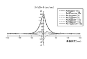
- the graph which shows the relationship between sputtering gas introduction
- the graph which shows the relationship between the energization current to a coil, and a sputtering rate.
- the sputtering apparatus M includes a vacuum chamber 1 that can form a vacuum atmosphere, and a cathode unit C is attached to the ceiling of the vacuum chamber 1.
- the ceiling side of the vacuum chamber 1 is referred to as “upper” and the bottom side thereof is referred to as “lower”.
- the cathode unit C includes a cylindrical holder 2 made of a conductive material, for example, the same material as a target material described later.
- One recess 3 is formed in the center of the lower surface of the holder 2.
- the opening area of the recess 3 is set in the range of ⁇ 30 to 50 mm, and the target material 4 is inserted into the recess 3.
- the target material 4 is made of a material appropriately selected according to the composition of the thin film to be formed on the substrate W to be processed, for example, made of Cu, Ti, or Ta, and has a discharge space 4a inside. It has a bottom cylindrical shape and is detachably inserted into the recess 3 from the bottom side. The length of the target material 4 is set so that the lower surface thereof is flush with the lower surface of the holder 2.
- a plurality of accommodation holes 5 extending in the thickness direction are opened on the upper surface of the holder 2, and magnets 6 formed into a cylindrical shape or a prismatic shape are inserted to constitute a magnetic field generating means.
- eight accommodation holes 5 are formed at intervals of 45 degrees in the circumferential direction of the holder 2, and two accommodation holes 5 are provided at predetermined intervals in the thickness direction of the holder 2.
- These prismatic magnets 6 are provided by alternately changing the polarity on the target material 4 side, and generate a strong magnetic field of 500 gauss or more in the space 4a.
- a disk-like support 7 is mounted, and the cathode unit C is mounted via an insulator (not shown). Further, the holder 2 is connected to a DC power source E1 which is a sputtering power source, and a negative DC potential is applied to the holder 2 and consequently the target material 4 during sputtering. Note that the sputtering power source is not limited to this, and other known power sources can be used.
- an anode shield 8 having conductivity is disposed below the holder 2.
- the anode shield 8 has a shape that covers the entire lower surface of the holder 2, and includes an opening 8 a that the target material 4 faces.
- a hollow cylindrical portion 8b extending toward the substrate W side is formed at the periphery of the opening 8a.
- the anode shield 8 is connected to another DC power source E2, and a positive DC potential is applied during sputtering. Thereby, the cylindrical part 8b plays a role of assisting the ions of the sputtered particles to be emitted from the space 4a of the target material 4 to the substrate W with strong straightness.
- a stage 9 is disposed at the bottom of the vacuum chamber 1 so as to face the cathode unit C, and a substrate W to be processed such as a silicon wafer can be positioned and held.
- a high frequency power source E3 is connected to the stage 9, and a bias potential is applied to the stage 9 and eventually the substrate W during sputtering, and ions of sputtered particles and sputter gas ions from the target material 4 are actively drawn into the substrate W. It is.
- the inner wall of the vacuum chamber 1 is provided with a pair of upper and lower protective plates 10u, 10d, which define a sputter chamber in the vacuum chamber 1 and prevent sputter particles from adhering to the inner wall of the vacuum chamber 1 or the like.
- a gas pipe 11 for introducing a sputtering gas which is a rare gas such as argon, is connected to the side wall of the vacuum chamber 1, and the other end communicates with a gas source (not shown) via a mass flow controller 12.
- these components constitute gas introduction means, and the sputter gas whose flow rate is controlled can be introduced into the vacuum chamber 1.
- an exhaust pipe 14 communicating with a vacuum exhaust means 13 such as a turbo molecular pump or a rotary pump is connected to the bottom of the vacuum chamber 1.
- an upper coil 15u and a lower coil 15d are provided around the reference axis CL connecting the centers of the cathode unit C and the substrate W with a predetermined interval in the vertical direction.
- the vertical magnetic field generation is performed so that the upper and lower coils 15u and 15d and the DC power source E4 generate a vertical magnetic field so that perpendicular magnetic field lines pass from the cathode unit C to the entire surface of the substrate W at equal intervals.
- the direction of the sputtered particles and the ions of the sputtered particles from the target material 4 is changed by the vertical magnetic field, and enters and adheres to the substrate W substantially perpendicularly.
- the DC power source E4 is preferably configured to be able to arbitrarily change the current value and the direction of the current to the upper and lower coils 15u, 15d.
- the magnetic field strength becomes 100 Gauss or more.
- an energization current (for example, 15 A or less) is set. If it is less than 100 gauss, the plasma is deactivated and film formation cannot be performed satisfactorily.
- the upper and lower coils 15u and 15d are caused to generate an upward vertical magnetic field.
- the direction of the flowing current is controlled.
- the number of coils is not limited to the above.
- the sputtering apparatus M includes a known control means 16 having a microcomputer, a sequencer and the like.
- the control means 16 operates the DC power sources and the high frequency power sources E1 to E4, the mass flow controller 12 and the vacuum exhaust means 13. The operation etc. is supervised and managed.
- a silicon oxide film (insulating film) is formed on the surface of the Si wafer as the substrate W to be formed, and then this silicon oxide film is formed by a known method.
- An example will be described in which a Cu film as a seed film is formed by sputtering using a pattern formed by patterning fine holes for wiring.
- the target material 4 is fitted and inserted into the recess 3 of the holder 2, and the magnet 6 is disposed in the accommodation hole 5 from the upper side, and then the support 7 is attached and the cathode unit C is assembled. Then, the cathode unit C is mounted on the ceiling portion of the vacuum chamber 1 via an insulator.
- the vacuum exhaust means 13 is operated to evacuate the vacuum chamber 1 to a predetermined degree of vacuum (for example, 10 ⁇ 5 Pa).
- a predetermined degree of vacuum for example, 10 ⁇ 5 Pa.
- the mass flow controller 12 is controlled to introduce a sputtering gas into the vacuum chamber 1 at a predetermined flow rate.
- the DC power source E4 energizes the upper and lower coils 15u and 15d to generate a vertical magnetic field so that vertical magnetic field lines pass from the cathode unit C over the entire surface of the substrate W at equal intervals, and the DC power source is supplied to the anode shield 8.
- a positive potential for example, 5 to 150 V
- a negative potential for example, 200 to 600 V
- a negative bias potential for example, for example, to the substrate W by the high frequency power source E3. 100 to 600 V) is applied.
- glow discharge is generated in the space 4 a inside the target material 4 from the space in front of the cathode unit C, and plasma is confined in the space 4 a by the magnetic field generated by the magnet 6. Thereafter, when the introduction of the sputtering gas is stopped by controlling the mass flow controller 12, self-discharge is performed in the space 4a under a low pressure.
- argon ions or the like in the plasma collide with the inner wall surface of the target material 4 and are sputtered, Cu atoms are scattered, and Cu atoms or ionized Cu ions are strongly straight from the opening on the lower surface of each target material 4.
- the sputtered particles or the ions of the sputtered particles whose direction is changed by the vertical magnetic field are combined with the application of the bias potential and the generation of the vertical magnetic field. However, they are attracted and deposited almost vertically with respect to the substrate W.
- the mass flow controller 12 is controlled to be turned on / off by the control means 16 at a predetermined cycle, and the sputtering gas is introduced into the vacuum chamber 1 at a predetermined flow rate.
- the introduction period of the sputtering gas is set in consideration of the gas exhaust speed and the like.
- the sputtering gas introduction time is set in the range of 0.5 to 2.5 sec in consideration of the gas exhaust speed and the like.
- the etching rate can be controlled by changing the vertical magnetic field strength or the gas flow rate of the inert gas.
- the gas flow rate may be adjusted within a range of 3 to 100 sccm, for example.
- the flow rate is 3 sccm or less, there is a problem that the gas flow rate control becomes unstable, and when the flow rate exceeds 100 sccm, the gas exhaust time becomes long.
- a Cu film was formed using the sputtering apparatus shown in FIG.
- the substrate W is formed by forming a silicon oxide film over the entire surface of a ⁇ 300 mm Si wafer and then patterning fine holes (width 40 nm, depth 140 nm) in the silicon oxide film by a known method.
- the target material 4 made of Cu having a composition ratio of 99% and having a thickness of 5 mm and an opening diameter of the lower surface of 30 mm was used.
- the distance between the lower surface of the holder 2 and the substrate W is set to 300 mm
- the input power to the target material 4 is 6.6 kW (current 19.5 A)
- the input voltage to the anode shield 8 is 150 V
- a Cu film was formed by setting an energization current 30A to each of the coils 15u and 15d, a bias power of 0 kW, and a sputtering time of 15 seconds.
- Ar was used as the sputtering gas, and the sputtering gas was introduced at a flow rate of 100 sccm for 1 second at the beginning of the film formation by sputtering, and then introduced into the vacuum chamber 1 at each flow rate of 0 to 100 sccm.
- FIG. 3 is a graph showing measured values of the sputtering rate when the film is formed under the above conditions. According to this, when the flow rate of the sputtering gas is smaller than 3 sccm, a high sputtering rate exceeding 3 nm / sec is obtained, and the film thickness distribution is extremely uniform immediately below and around the opening of the cathode material 4. It was confirmed that it was higher.
- the flow rate of the sputtering gas exceeds 3 sccm
- the sputtering rate particularly at a position immediately below the opening of the target material 4 is extremely lowered, and the Cu film deposited and deposited on the surface of the substrate W may be etched. It could be confirmed. In this case, it was also confirmed that the etching amount increased as the bias power was increased.
- the deposition conditions are the same as above except that the sputtering gas is introduced at a flow rate of 100 sccm for the first 1 seconds after the film formation is started, and then the gas introduction is stopped, and the upper and lower coils 15u and 15d are applied to the upper and lower coils 15u and 15d.
- the energization current was changed. *
- the cathode unit may be configured by forming a large number of recesses densely over the entire lower surface of the holder 2 and inserting a target material into each recess.
- M Sputtering device 1 Vacuum chamber 2 Holder (Cathode unit) 3 recess 4 Target material (cathode unit) 6 Magnet (magnetic field generation means) 11 Gas pipe (gas introduction means) 12 Mass flow controller (gas introduction means) 15u upper coil (vertical magnetic field generating means) 15d Lower coil (vertical magnetic field generating means) C cathode unit E1 to E4 power supply W substrate
Landscapes
- Chemical & Material Sciences (AREA)
- Engineering & Computer Science (AREA)
- Physics & Mathematics (AREA)
- Plasma & Fusion (AREA)
- Materials Engineering (AREA)
- Chemical Kinetics & Catalysis (AREA)
- Analytical Chemistry (AREA)
- Mechanical Engineering (AREA)
- Metallurgy (AREA)
- Organic Chemistry (AREA)
- Electromagnetism (AREA)
- Electrodes Of Semiconductors (AREA)
- Physical Vapour Deposition (AREA)
Abstract
Description
1 真空チャンバ
2 ホルダ(カソードユニット)
3 凹部
4 ターゲット材(カソードユニット)
6 マグネット(磁場発生手段)
11 ガス管(ガス導入手段)
12 マスフローコントローラ(ガス導入手段)
15u 上コイル(垂直磁場発生手段)
15d 下コイル(垂直磁場発生手段)
C カソードユニット
E1乃至E4 電源
W 基板
Claims (4)
- 処理すべき基板が配置される真空チャンバと、
真空チャンバ内で基板に対向配置され、ホルダの片面に形成された少なくとも1個の凹部に有底筒状のターゲット材をその底部側から装着すると共にターゲット材の内部空間に磁場を発生させる磁場発生手段を組み付けてなるカソードユニットと、
前記ホルダのうち基板との対向面を少なくとも覆うように配置され、正電位が印加されるアノードシールドと、
前記真空チャンバ内に所定のスパッタガスを導入するガス導入手段と、
前記カソードユニットに電力投入するスパッタ電源と、
前記カソードユニットと基板とを結ぶ基準軸の回りで真空チャンバの壁面に設けたコイル及び各コイルへの通電を可能とする電源とからなる垂直磁場発生手段と、
前記ガス導入手段からのスパッタガスの導入をオンオフ制御する制御手段とを備えたことを特徴とするスパッタリング装置。 - アノードシールドは、ターゲット材を臨む開口部と、開口部の周縁に形成された基板側に向かって延出する筒状部とを備えることを特徴とする請求項1記載のスパッタリング装置。
- 請求項1または請求項2記載のスパッタリング装置にて処理すべき基板の表面に成膜するスパッタリング方法であって、前記垂直磁場発生手段によりターゲット材と基板表面との間に所定の間隔で垂直な磁力線が通るように垂直磁場を発生させ、前記ガス導入手段により真空チャンバ内にスパッタガスを導入し、アノードシールドに正電位を印加すると共にカソードユニットに負電位を印加してターゲット材の内壁面をスパッタリングし、スパッタリング中、前記制御手段によりスパッタガスの導入を所定の間隔でオンオフすることを特徴とするスパッタリング方法。
- 前記基板にバイアス電位を印加することを特徴とする請求項2記載のスパッタリング方法。
Priority Applications (5)
| Application Number | Priority Date | Filing Date | Title |
|---|---|---|---|
| US13/130,589 US8834685B2 (en) | 2008-12-15 | 2009-12-08 | Sputtering apparatus and sputtering method |
| CN200980150338.2A CN102245798A (zh) | 2008-12-15 | 2009-12-08 | 溅镀装置及溅镀方法 |
| DE112009003766T DE112009003766T8 (de) | 2008-12-15 | 2009-12-08 | Sputter-Vorrichtung und Sputter-Verfahren |
| JP2010542842A JP5550565B2 (ja) | 2008-12-15 | 2009-12-08 | スパッタリング装置及びスパッタリング方法 |
| SG2011037330A SG171398A1 (en) | 2008-12-15 | 2009-12-08 | Sputtering apparatus and sputtering method |
Applications Claiming Priority (2)
| Application Number | Priority Date | Filing Date | Title |
|---|---|---|---|
| JP2008-318990 | 2008-12-15 | ||
| JP2008318990 | 2008-12-15 |
Publications (1)
| Publication Number | Publication Date |
|---|---|
| WO2010070845A1 true WO2010070845A1 (ja) | 2010-06-24 |
Family
ID=42268527
Family Applications (1)
| Application Number | Title | Priority Date | Filing Date |
|---|---|---|---|
| PCT/JP2009/006699 Ceased WO2010070845A1 (ja) | 2008-12-15 | 2009-12-08 | スパッタリング装置及びスパッタリング方法 |
Country Status (8)
| Country | Link |
|---|---|
| US (1) | US8834685B2 (ja) |
| JP (1) | JP5550565B2 (ja) |
| KR (1) | KR101593544B1 (ja) |
| CN (1) | CN102245798A (ja) |
| DE (1) | DE112009003766T8 (ja) |
| SG (1) | SG171398A1 (ja) |
| TW (1) | TWI490929B (ja) |
| WO (1) | WO2010070845A1 (ja) |
Cited By (3)
| Publication number | Priority date | Publication date | Assignee | Title |
|---|---|---|---|---|
| WO2016136255A1 (ja) * | 2015-02-25 | 2016-09-01 | 株式会社アルバック | 成膜装置及び成膜方法 |
| CN110777337A (zh) * | 2018-07-31 | 2020-02-11 | 佳能特机株式会社 | 成膜装置以及电子器件的制造方法 |
| JP2025005540A (ja) * | 2023-06-28 | 2025-01-17 | エドワーズ株式会社 | 真空排気システム、及び真空ポンプ |
Families Citing this family (7)
| Publication number | Priority date | Publication date | Assignee | Title |
|---|---|---|---|---|
| TWI485277B (zh) * | 2013-12-13 | 2015-05-21 | Univ Minghsin Sci & Tech | 多靶反應性濺鍍製程穩定控制方法 |
| GB201505578D0 (en) * | 2015-03-31 | 2015-05-13 | Spts Technologies Ltd | Method and apparatus for depositing a material |
| CN106637103B (zh) * | 2016-10-12 | 2019-04-05 | 南京华东电子信息科技股份有限公司 | 一种igzo成膜设备的阳极稳定装置 |
| CN108456860B (zh) * | 2017-02-22 | 2020-12-08 | 北京北方华创微电子装备有限公司 | 一种沉积腔室和膜层沉积装置 |
| CN109314025B (zh) * | 2017-04-06 | 2020-05-15 | 株式会社爱发科 | 离子源以及离子注入装置 |
| CN115404450B (zh) * | 2021-05-28 | 2023-12-05 | 鑫天虹(厦门)科技有限公司 | 磁场分布调整装置、沉积设备及其沉积方法 |
| US12476090B2 (en) * | 2021-12-09 | 2025-11-18 | Ulvac, Inc. | Method of depositing silicon nitride film, apparatus for depositing film, and silicon nitride film |
Citations (8)
| Publication number | Priority date | Publication date | Assignee | Title |
|---|---|---|---|---|
| JPS60184676A (ja) * | 1984-02-11 | 1985-09-20 | グリコ‐メタル‐ヴエルケ・デーレン・ウント・ロース・ゲゼルシヤフト・ミツト・ベシユレンクテル・ハフツング | 有被覆基材または有被覆部材の製造法 |
| JPS6188511A (ja) * | 1984-10-05 | 1986-05-06 | Nec Kansai Ltd | 磁性体薄膜製作方法 |
| JPS6277460A (ja) * | 1985-09-30 | 1987-04-09 | Tokuda Seisakusho Ltd | 放電電極 |
| JPH02175864A (ja) * | 1988-12-27 | 1990-07-09 | Toshiba Corp | 薄膜形成装置およびこれを用いた薄膜形成方法 |
| JPH07118845A (ja) * | 1993-10-25 | 1995-05-09 | Asahi Glass Co Ltd | マグネトロンスパッタリング装置 |
| JPH07183219A (ja) * | 1993-10-08 | 1995-07-21 | Varian Assoc Inc | プラズマからのイオン抽出を採用するpvd装置 |
| JP2002080962A (ja) * | 2000-09-07 | 2002-03-22 | Ulvac Japan Ltd | スパッタリング装置及び薄膜製造方法 |
| JP2006169610A (ja) * | 2004-12-20 | 2006-06-29 | Matsushita Electric Ind Co Ltd | スパッタリング装置 |
Family Cites Families (14)
| Publication number | Priority date | Publication date | Assignee | Title |
|---|---|---|---|---|
| GB1154249A (en) | 1966-10-12 | 1969-06-04 | Arnex Products Ltd | Improvements in or relating to Folding Tables |
| JPS61261473A (ja) * | 1985-05-15 | 1986-11-19 | Tokuda Seisakusho Ltd | スパツタリング装置 |
| JP3069180B2 (ja) * | 1991-11-15 | 2000-07-24 | 東京エレクトロン株式会社 | 中空形状マグネトロンスパッタ電極 |
| US5997699A (en) * | 1996-04-08 | 1999-12-07 | Micron Technology Inc. | Insitu faceting during deposition |
| US5976334A (en) * | 1997-11-25 | 1999-11-02 | Applied Materials, Inc. | Reliable sustained self-sputtering |
| US5976224A (en) * | 1998-05-04 | 1999-11-02 | Durant; James F. | Separating carbon from ash |
| JP5026631B2 (ja) * | 1999-06-24 | 2012-09-12 | 株式会社アルバック | スパッタリング装置 |
| JP4021601B2 (ja) * | 1999-10-29 | 2007-12-12 | 株式会社東芝 | スパッタ装置および成膜方法 |
| CN100355058C (zh) * | 2001-05-04 | 2007-12-12 | 东京毅力科创株式会社 | 具有连续沉积和蚀刻的电离pvd |
| US7504006B2 (en) * | 2002-08-01 | 2009-03-17 | Applied Materials, Inc. | Self-ionized and capacitively-coupled plasma for sputtering and resputtering |
| JP2005105400A (ja) * | 2003-10-02 | 2005-04-21 | Canon Inc | 成膜装置、成膜方法、光学素子、及び光学系 |
| JP2008047661A (ja) | 2006-08-14 | 2008-02-28 | Seiko Epson Corp | 成膜装置及び半導体装置の製造方法 |
| JP2008167175A (ja) | 2006-12-28 | 2008-07-17 | Audio Technica Corp | バウンダリーマイクロホン |
| WO2009157438A1 (ja) | 2008-06-26 | 2009-12-30 | 株式会社アルバック | カソードユニット及びこのカソードユニットを備えたスパッタリング装置 |
-
2009
- 2009-12-08 JP JP2010542842A patent/JP5550565B2/ja active Active
- 2009-12-08 KR KR1020117013198A patent/KR101593544B1/ko active Active
- 2009-12-08 WO PCT/JP2009/006699 patent/WO2010070845A1/ja not_active Ceased
- 2009-12-08 US US13/130,589 patent/US8834685B2/en active Active
- 2009-12-08 DE DE112009003766T patent/DE112009003766T8/de not_active Ceased
- 2009-12-08 CN CN200980150338.2A patent/CN102245798A/zh active Pending
- 2009-12-08 SG SG2011037330A patent/SG171398A1/en unknown
- 2009-12-14 TW TW098142717A patent/TWI490929B/zh active
Patent Citations (8)
| Publication number | Priority date | Publication date | Assignee | Title |
|---|---|---|---|---|
| JPS60184676A (ja) * | 1984-02-11 | 1985-09-20 | グリコ‐メタル‐ヴエルケ・デーレン・ウント・ロース・ゲゼルシヤフト・ミツト・ベシユレンクテル・ハフツング | 有被覆基材または有被覆部材の製造法 |
| JPS6188511A (ja) * | 1984-10-05 | 1986-05-06 | Nec Kansai Ltd | 磁性体薄膜製作方法 |
| JPS6277460A (ja) * | 1985-09-30 | 1987-04-09 | Tokuda Seisakusho Ltd | 放電電極 |
| JPH02175864A (ja) * | 1988-12-27 | 1990-07-09 | Toshiba Corp | 薄膜形成装置およびこれを用いた薄膜形成方法 |
| JPH07183219A (ja) * | 1993-10-08 | 1995-07-21 | Varian Assoc Inc | プラズマからのイオン抽出を採用するpvd装置 |
| JPH07118845A (ja) * | 1993-10-25 | 1995-05-09 | Asahi Glass Co Ltd | マグネトロンスパッタリング装置 |
| JP2002080962A (ja) * | 2000-09-07 | 2002-03-22 | Ulvac Japan Ltd | スパッタリング装置及び薄膜製造方法 |
| JP2006169610A (ja) * | 2004-12-20 | 2006-06-29 | Matsushita Electric Ind Co Ltd | スパッタリング装置 |
Cited By (7)
| Publication number | Priority date | Publication date | Assignee | Title |
|---|---|---|---|---|
| WO2016136255A1 (ja) * | 2015-02-25 | 2016-09-01 | 株式会社アルバック | 成膜装置及び成膜方法 |
| JPWO2016136255A1 (ja) * | 2015-02-25 | 2017-04-27 | 株式会社アルバック | 成膜装置及び成膜方法 |
| KR101926677B1 (ko) * | 2015-02-25 | 2018-12-07 | 가부시키가이샤 알박 | 성막 장치 및 성막 방법 |
| CN110777337A (zh) * | 2018-07-31 | 2020-02-11 | 佳能特机株式会社 | 成膜装置以及电子器件的制造方法 |
| CN110777337B (zh) * | 2018-07-31 | 2023-05-02 | 佳能特机株式会社 | 成膜装置以及电子器件的制造方法 |
| JP2025005540A (ja) * | 2023-06-28 | 2025-01-17 | エドワーズ株式会社 | 真空排気システム、及び真空ポンプ |
| JP7802729B2 (ja) | 2023-06-28 | 2026-01-20 | エドワーズ株式会社 | 真空排気システム、及び真空ポンプ |
Also Published As
| Publication number | Publication date |
|---|---|
| TW201030822A (en) | 2010-08-16 |
| US20110247928A1 (en) | 2011-10-13 |
| US8834685B2 (en) | 2014-09-16 |
| JP5550565B2 (ja) | 2014-07-16 |
| KR20110103950A (ko) | 2011-09-21 |
| JPWO2010070845A1 (ja) | 2012-05-24 |
| DE112009003766T5 (de) | 2012-10-04 |
| TWI490929B (zh) | 2015-07-01 |
| SG171398A1 (en) | 2011-07-28 |
| CN102245798A (zh) | 2011-11-16 |
| KR101593544B1 (ko) | 2016-02-15 |
| DE112009003766T8 (de) | 2012-10-25 |
Similar Documents
| Publication | Publication Date | Title |
|---|---|---|
| JP5550565B2 (ja) | スパッタリング装置及びスパッタリング方法 | |
| JP5373905B2 (ja) | 成膜装置及び成膜方法 | |
| JP5417437B2 (ja) | 成膜方法及び成膜装置 | |
| JP4344019B2 (ja) | イオン化スパッタ方法 | |
| JP4976132B2 (ja) | 金属のイオン物理蒸着におけるスパッタリングソース | |
| JPWO2009157439A1 (ja) | スパッタリング装置及びスパッタリング方法 | |
| JP5717444B2 (ja) | カソードユニット及びこのカソードユニットを備えたスパッタリング装置 | |
| KR101429069B1 (ko) | 성막 장치 및 성막 방법 | |
| KR20170041903A (ko) | 성막 장치 및 성막 방법 | |
| JP2007197840A (ja) | イオン化スパッタ装置 | |
| JP4526139B2 (ja) | 基板処理装置及びスパッタリング装置 | |
| JP5693175B2 (ja) | スパッタリング方法 | |
| JP5795002B2 (ja) | スパッタリング方法 | |
| JP2011179068A (ja) | 金属薄膜の形成方法 | |
| JP2015178653A (ja) | スパッタリング装置及びスパッタリング方法 |
Legal Events
| Date | Code | Title | Description |
|---|---|---|---|
| WWE | Wipo information: entry into national phase |
Ref document number: 200980150338.2 Country of ref document: CN |
|
| 121 | Ep: the epo has been informed by wipo that ep was designated in this application |
Ref document number: 09833155 Country of ref document: EP Kind code of ref document: A1 |
|
| ENP | Entry into the national phase |
Ref document number: 2010542842 Country of ref document: JP Kind code of ref document: A |
|
| ENP | Entry into the national phase |
Ref document number: 20117013198 Country of ref document: KR Kind code of ref document: A |
|
| WWE | Wipo information: entry into national phase |
Ref document number: 112009003766 Country of ref document: DE Ref document number: 1120090037666 Country of ref document: DE |
|
| WWE | Wipo information: entry into national phase |
Ref document number: 13130589 Country of ref document: US |
|
| 122 | Ep: pct application non-entry in european phase |
Ref document number: 09833155 Country of ref document: EP Kind code of ref document: A1 |