WO2010061844A1 - 太陽電池モジュール及びその製造方法 - Google Patents
太陽電池モジュール及びその製造方法 Download PDFInfo
- Publication number
- WO2010061844A1 WO2010061844A1 PCT/JP2009/069846 JP2009069846W WO2010061844A1 WO 2010061844 A1 WO2010061844 A1 WO 2010061844A1 JP 2009069846 W JP2009069846 W JP 2009069846W WO 2010061844 A1 WO2010061844 A1 WO 2010061844A1
- Authority
- WO
- WIPO (PCT)
- Prior art keywords
- opening
- lead wire
- sheet
- solar cell
- back surface
- Prior art date
Links
- 238000004519 manufacturing process Methods 0.000 title claims abstract description 14
- 238000000034 method Methods 0.000 title abstract description 22
- 239000000758 substrate Substances 0.000 claims abstract description 14
- 238000006243 chemical reaction Methods 0.000 claims abstract description 12
- WABPQHHGFIMREM-UHFFFAOYSA-N lead(0) Chemical compound [Pb] WABPQHHGFIMREM-UHFFFAOYSA-N 0.000 claims description 171
- 238000009413 insulation Methods 0.000 claims description 38
- 229920005989 resin Polymers 0.000 claims description 18
- 239000011347 resin Substances 0.000 claims description 18
- 239000000853 adhesive Substances 0.000 claims description 16
- 230000001070 adhesive effect Effects 0.000 claims description 16
- 239000000463 material Substances 0.000 claims description 5
- 239000010408 film Substances 0.000 description 260
- 238000007789 sealing Methods 0.000 description 37
- 239000005038 ethylene vinyl acetate Substances 0.000 description 24
- 229920001200 poly(ethylene-vinyl acetate) Polymers 0.000 description 24
- 238000000576 coating method Methods 0.000 description 14
- 238000010030 laminating Methods 0.000 description 14
- 239000011248 coating agent Substances 0.000 description 13
- 229920000139 polyethylene terephthalate Polymers 0.000 description 10
- 239000005020 polyethylene terephthalate Substances 0.000 description 10
- 239000004820 Pressure-sensitive adhesive Substances 0.000 description 9
- 230000001681 protective effect Effects 0.000 description 7
- RYGMFSIKBFXOCR-UHFFFAOYSA-N Copper Chemical compound [Cu] RYGMFSIKBFXOCR-UHFFFAOYSA-N 0.000 description 6
- 239000011889 copper foil Substances 0.000 description 6
- 229920002620 polyvinyl fluoride Polymers 0.000 description 6
- 238000007599 discharging Methods 0.000 description 5
- 238000005452 bending Methods 0.000 description 4
- 238000003475 lamination Methods 0.000 description 4
- 230000004048 modification Effects 0.000 description 4
- 238000012986 modification Methods 0.000 description 4
- 230000015556 catabolic process Effects 0.000 description 3
- 229920002037 poly(vinyl butyral) polymer Polymers 0.000 description 3
- 238000010248 power generation Methods 0.000 description 3
- 238000005476 soldering Methods 0.000 description 3
- 230000002093 peripheral effect Effects 0.000 description 2
- -1 polyethylene terephthalate Polymers 0.000 description 2
- 239000010409 thin film Substances 0.000 description 2
- QTBSBXVTEAMEQO-UHFFFAOYSA-M Acetate Chemical compound CC([O-])=O QTBSBXVTEAMEQO-UHFFFAOYSA-M 0.000 description 1
- 229920002799 BoPET Polymers 0.000 description 1
- 229910004613 CdTe Inorganic materials 0.000 description 1
- YCKRFDGAMUMZLT-UHFFFAOYSA-N Fluorine atom Chemical compound [F] YCKRFDGAMUMZLT-UHFFFAOYSA-N 0.000 description 1
- 239000004642 Polyimide Substances 0.000 description 1
- XUIMIQQOPSSXEZ-UHFFFAOYSA-N Silicon Chemical compound [Si] XUIMIQQOPSSXEZ-UHFFFAOYSA-N 0.000 description 1
- 229910006404 SnO 2 Inorganic materials 0.000 description 1
- 229910021417 amorphous silicon Inorganic materials 0.000 description 1
- 230000004888 barrier function Effects 0.000 description 1
- DQXBYHZEEUGOBF-UHFFFAOYSA-N but-3-enoic acid;ethene Chemical compound C=C.OC(=O)CC=C DQXBYHZEEUGOBF-UHFFFAOYSA-N 0.000 description 1
- 150000001875 compounds Chemical class 0.000 description 1
- 238000006073 displacement reaction Methods 0.000 description 1
- 230000000694 effects Effects 0.000 description 1
- 239000000945 filler Substances 0.000 description 1
- 229910052731 fluorine Inorganic materials 0.000 description 1
- 239000011737 fluorine Substances 0.000 description 1
- 239000011521 glass Substances 0.000 description 1
- 229920006015 heat resistant resin Polymers 0.000 description 1
- 230000007774 longterm Effects 0.000 description 1
- 239000011159 matrix material Substances 0.000 description 1
- 239000012528 membrane Substances 0.000 description 1
- 229910021424 microcrystalline silicon Inorganic materials 0.000 description 1
- 239000000203 mixture Substances 0.000 description 1
- 229920001721 polyimide Polymers 0.000 description 1
- 229920001296 polysiloxane Polymers 0.000 description 1
- 238000004080 punching Methods 0.000 description 1
- 239000003566 sealing material Substances 0.000 description 1
- 229910052710 silicon Inorganic materials 0.000 description 1
- 239000010703 silicon Substances 0.000 description 1
- 229910000679 solder Inorganic materials 0.000 description 1
- 229920001169 thermoplastic Polymers 0.000 description 1
- 238000003466 welding Methods 0.000 description 1
Images


Classifications
-
- H—ELECTRICITY
- H01—ELECTRIC ELEMENTS
- H01L—SEMICONDUCTOR DEVICES NOT COVERED BY CLASS H10
- H01L31/00—Semiconductor devices sensitive to infrared radiation, light, electromagnetic radiation of shorter wavelength or corpuscular radiation and specially adapted either for the conversion of the energy of such radiation into electrical energy or for the control of electrical energy by such radiation; Processes or apparatus specially adapted for the manufacture or treatment thereof or of parts thereof; Details thereof
- H01L31/04—Semiconductor devices sensitive to infrared radiation, light, electromagnetic radiation of shorter wavelength or corpuscular radiation and specially adapted either for the conversion of the energy of such radiation into electrical energy or for the control of electrical energy by such radiation; Processes or apparatus specially adapted for the manufacture or treatment thereof or of parts thereof; Details thereof adapted as photovoltaic [PV] conversion devices
- H01L31/042—PV modules or arrays of single PV cells
- H01L31/048—Encapsulation of modules
- H01L31/0488—Double glass encapsulation, e.g. photovoltaic cells arranged between front and rear glass sheets
-
- H—ELECTRICITY
- H01—ELECTRIC ELEMENTS
- H01L—SEMICONDUCTOR DEVICES NOT COVERED BY CLASS H10
- H01L31/00—Semiconductor devices sensitive to infrared radiation, light, electromagnetic radiation of shorter wavelength or corpuscular radiation and specially adapted either for the conversion of the energy of such radiation into electrical energy or for the control of electrical energy by such radiation; Processes or apparatus specially adapted for the manufacture or treatment thereof or of parts thereof; Details thereof
- H01L31/02—Details
- H01L31/02002—Arrangements for conducting electric current to or from the device in operations
- H01L31/02005—Arrangements for conducting electric current to or from the device in operations for device characterised by at least one potential jump barrier or surface barrier
- H01L31/02008—Arrangements for conducting electric current to or from the device in operations for device characterised by at least one potential jump barrier or surface barrier for solar cells or solar cell modules
- H01L31/02013—Arrangements for conducting electric current to or from the device in operations for device characterised by at least one potential jump barrier or surface barrier for solar cells or solar cell modules comprising output lead wires elements
-
- H—ELECTRICITY
- H01—ELECTRIC ELEMENTS
- H01L—SEMICONDUCTOR DEVICES NOT COVERED BY CLASS H10
- H01L31/00—Semiconductor devices sensitive to infrared radiation, light, electromagnetic radiation of shorter wavelength or corpuscular radiation and specially adapted either for the conversion of the energy of such radiation into electrical energy or for the control of electrical energy by such radiation; Processes or apparatus specially adapted for the manufacture or treatment thereof or of parts thereof; Details thereof
- H01L31/04—Semiconductor devices sensitive to infrared radiation, light, electromagnetic radiation of shorter wavelength or corpuscular radiation and specially adapted either for the conversion of the energy of such radiation into electrical energy or for the control of electrical energy by such radiation; Processes or apparatus specially adapted for the manufacture or treatment thereof or of parts thereof; Details thereof adapted as photovoltaic [PV] conversion devices
- H01L31/042—PV modules or arrays of single PV cells
- H01L31/048—Encapsulation of modules
- H01L31/049—Protective back sheets
-
- H—ELECTRICITY
- H02—GENERATION; CONVERSION OR DISTRIBUTION OF ELECTRIC POWER
- H02S—GENERATION OF ELECTRIC POWER BY CONVERSION OF INFRARED RADIATION, VISIBLE LIGHT OR ULTRAVIOLET LIGHT, e.g. USING PHOTOVOLTAIC [PV] MODULES
- H02S40/00—Components or accessories in combination with PV modules, not provided for in groups H02S10/00 - H02S30/00
- H02S40/30—Electrical components
- H02S40/34—Electrical components comprising specially adapted electrical connection means to be structurally associated with the PV module, e.g. junction boxes
-
- Y—GENERAL TAGGING OF NEW TECHNOLOGICAL DEVELOPMENTS; GENERAL TAGGING OF CROSS-SECTIONAL TECHNOLOGIES SPANNING OVER SEVERAL SECTIONS OF THE IPC; TECHNICAL SUBJECTS COVERED BY FORMER USPC CROSS-REFERENCE ART COLLECTIONS [XRACs] AND DIGESTS
- Y02—TECHNOLOGIES OR APPLICATIONS FOR MITIGATION OR ADAPTATION AGAINST CLIMATE CHANGE
- Y02E—REDUCTION OF GREENHOUSE GAS [GHG] EMISSIONS, RELATED TO ENERGY GENERATION, TRANSMISSION OR DISTRIBUTION
- Y02E10/00—Energy generation through renewable energy sources
- Y02E10/50—Photovoltaic [PV] energy
Definitions
- a solar battery cell is stacked on a translucent insulating substrate, and a lead wire in an insulating state and an opening for leading out an output lead portion of the lead wire on the back surface electrode film of the solar battery cell
- the present invention relates to a solar cell module having a structure in which a back surface protection sheet having a plurality of layers is sequentially stacked, and a method of manufacturing the same.
- a solar power generation system that performs solar power generation by laying a solar cell module in which a plurality of solar cell strings are arranged in a matrix on a roof or the like of a building has begun to be widely spread.
- each solar cell module is provided with a terminal box for making it possible to electrically connect the other solar cell modules installed adjacent to each other.
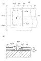
- FIG.23 (a), (b) and FIG. One structural example of the solar cell string which comprises the conventional solar cell module is shown in FIG.23 (a), (b) and FIG.
- FIG.23 (a), (b) is explanatory drawing which shows two scenes of a manufacturing process
- FIG. 24 is explanatory drawing which shows the process of carrying out lamination sealing of the solar cell string.
- FIG.23 and FIG.24 is described also in patent document 1.
- the photovoltaic cell 115 is formed by laminating a transparent electrode film made of a transparent conductive film, a photoelectric conversion layer, and a back surface electrode film in this order on the light-transmissive insulating substrate 111 although not shown.
- the solar battery cell 115 configured in this manner is an elongated rectangular shape as shown in FIG. 23A and has a length that covers almost the entire width of the light-transmissive insulating substrate 111, and adjacent solar battery cells 115. , 115 mutually connect one transparent electrode film and the other back surface electrode film, and the solar cell string 116 in which the several photovoltaic cell 115 was connected in series is comprised.
- a linear P-type electrode terminal portion 117 having substantially the same length as the solar battery cell 115 is formed on the end of the transparent electrode film of the solar battery cell 115 at one end of the solar cell string 116.
- a linear N-type electrode terminal portion 118 substantially the same length as the solar battery cell 115 is formed on the end of the back surface electrode film of the solar battery cell 115.
- the P-type electrode terminal portion 117 and the N-type electrode terminal portion 118 form an electrode lead-out portion.
- An insulating sheet 119 is laid on the solar cell string 116 so as to extend between the central portion of the P-type electrode terminal portion 117 and the central portion of the N-type electrode terminal portion 118.
- the insulating sheet 119 is laid so as not to overlap the P-type electrode terminal portion 117 and the N-type electrode terminal portion 118.
- a film compatible with the sealing material is preferable, and in particular, a PET film or a fluorine resin film is optimum.
- a resin sheet for bonding may be laid between the insulating sheet 119 and the solar battery cell 115 or between the insulating sheet 119 and the lead wire 112 or 113. It may be bonded in advance with an adhesive or the like.
- a positive electrode current collector 120 referred to as a bus bar made of copper foil having the same shape and size as the P-type electrode terminal portion 117 is electrically and mechanically joined to the entire surface of the P-type electrode terminal portion 117.
- a negative electrode current collector 121 having the same shape and size as the N-type electrode terminal portion 118 is electrically and mechanically joined to the entire surface of the N-type electrode terminal portion 118. Soldering or conductive paste can be used as these bonding means.
- a positive electrode lead wire 122 and a negative electrode lead wire 123 which are flat cables, are arranged in a straight line (or in a parallel state shifted in the width direction) with their distal end portions facing each other. ing.
- One end of the positive electrode lead wire 122 is connected to the central position of the positive electrode current collector 120. Also, the other end of the positive electrode lead wire 122 is located approximately at the center of the solar cell string 116 and is bent (for example, in a direction perpendicular to the surface) to rise from the surface of the solar cell string 116 It is an output lead portion 122a. Similarly, one end of the negative electrode lead wire 123 is connected to the center position of the negative electrode current collector 121. In addition, the other end of the negative electrode lead wire 123 is located approximately at the center of the solar cell string 116 and is bent (for example, in a direction perpendicular to the surface) to rise from the surface of the solar cell string 116 It is the output lead portion 123a.
- the positive electrode lead wire 122 and the negative electrode lead wire 123 straddle over the plurality of solar battery cells 115, but since the insulating sheet 119 is interposed between the positive electrode lead wire 122 and the solar battery cells 115, the plurality of solar battery cells 115 There is no short circuit.
- the width of the insulating sheet 119 is preferably sufficiently wider than the widths of the positive electrode lead wire 122 and the negative electrode lead wire 123, and the positive electrode current collector portion 120 to the negative electrode current collector portion 121 are arranged in the form of one strip sheet. There is.
- the sealing film is produced in a state where the output lead portions 122a and 123a of the positive electrode lead wire 122 and the negative electrode lead wire 123 are respectively derived from the openings 124a and 124a and the openings 125a and 125a.
- a back film 125 as a back surface protective material for weather resistance and high insulation is laminated and sealed on the entire surface of the solar cell string 116.
- a thermoplastic polymer film is preferable, and those made of EVA (ethylene vinyl acetate resin) or PVB (polyvinyl butyral resin) are most preferable.
- PET polyethylene terephthalate
- PVF polyvinyl fluoride resin film
- a terminal box not shown is attached and electrically connected.
- the opening 125a is formed in the back film 125 having the three-layer structure by punching or the like, the Al layer is exposed at the end face of the opening 125a. Therefore, the distance between the exposed end face of the Al layer and the back electrode film of the solar battery cell 115 becomes short, and there is a possibility that the discharge may occur when the withstand voltage test is performed. In particular, since a recent solar cell module has a high voltage and a high voltage is required as a withstand voltage, an accident due to a discharge is likely to occur with the above structure.
- each opening 125 a, 125 a of the back film 125 and each output lead there is a possibility that 122a and 123a may come in contact with each other. That is, since there is nothing to fix them in a relative positional relationship between the openings 125a, 125a and the output lead portions 122a, 123a, depending on the bending angle of the output lead portions 122a, 123a, the output lead portion There is a possibility that 122a and 123a come in contact with the openings 125a and 125a of the back film 125.
- Patent Document 2 The thin film solar cell module of Patent Document 2 is a Tedler sheet having a cut slightly larger than the hole of the protective cover on the sheet of the filler, as shown in FIGS. 5 (D) and 6 (E) thereof.
- Patent Document 2 solves a short circuit due to the contact between the end face of the Al layer exposed to the end face of the opening of the back film and the output lead portion.
- no consideration is given to the possibility that discharge may occur between the end face of the exposed Al layer and the back electrode film of the solar cell when performing the dielectric breakdown voltage test, and the solution is also suggested. It has not been.
- recent solar cell modules have a high voltage, and a high voltage is required as the withstand voltage.
- the present invention has been made to solve the above problems, and an object thereof is to provide a solar cell capable of sufficiently ensuring the withstand voltage between the back electrode film of the solar cell and the opening end face of the back surface protection sheet.
- solar cells comprising a transparent electrode film, a photoelectric conversion layer, and a back electrode film are stacked on a translucent insulating substrate, and the back electrode of this solar cell
- the present invention is applied to a solar cell module having a structure in which a lead wire in an insulating state and a back surface protection sheet having an opening for leading an output lead portion of the lead wire are sequentially stacked on a film.
- An insulating sheet is disposed between the electrode film and the back surface protection sheet so as to cover the entire periphery of the edge portion of the back surface protection sheet opening.
- a solar cell comprising a transparent electrode film, a photoelectric conversion layer, and a back surface electrode film is stacked on a translucent insulating substrate, and the back surface electrode film of the solar cell is formed.
- a method of manufacturing a solar cell module in which a lead wire in an insulated state and a back surface protection sheet having an opening for leading an output lead portion of the lead wire are sequentially stacked, the back surface electrode film and the back surface protection sheet And disposing the insulating sheet so as to cover the entire periphery of the edge of the back surface protection sheet opening.
- the back surface protective sheet includes a moistureproof layer such as a PET / Al / PET three-layer structure or a PVF / Al / PVF three-layer structure
- the end face of the Al layer is on the end face of the opening. It will be exposed. Therefore, discharge may occur between the end face of the Al layer and the back surface electrode film of the solar cell module, but in the present invention, the back surface protection sheet opening between the back surface electrode film and the back surface protection sheet Since the insulating sheet is disposed so as to cover the entire periphery of the part of the part, the discharge is prevented. Therefore, even if the withstand voltage test at a high voltage corresponding to a high voltage solar cell module is performed, a sufficient withstand voltage can be secured without discharging.
- the insulating sheet may be disposed at least along the entire periphery of the edge portion of the back surface protection sheet opening.
- a rectangular insulating sheet is formed along the four sides of the rectangular along each edge of the rectangular opening. You may arrange four in. That is, the insulating sheet may be absent at the central portion of the opening from which the output lead portion of the lead wire is led out.
- the insulating sheet is disposed between the lead wire and the back surface protection sheet, and the pressure sensitive adhesive on the lower surface of the insulation sheet fixes the lead wire on the back surface electrode film. It is also good. That is, according to the present invention, in addition to the original function of insulating between the back surface electrode film and the opening end face of the back surface protection sheet, the insulating sheet fixes the arrangement position of the lead wire wired on the back surface electrode film. It also functions as a fixing member. As a result, only by arranging the insulating sheet, it becomes possible to securely arrange and fix the lead wire at a position not in contact with the end face of the opening of the back surface protective sheet.
- the back surface electrode film and the back surface protection sheet are bonded using a resin sheet
- the back surface electrode film, the resin sheet, the lead wire, the insulating sheet, and the back surface protection sheet are stacked in this order
- the insulation sheet may be attached to the resin sheet by sandwiching the lead wire with the resin sheet and the insulation sheet.
- the resin sheet softens in the bonding process, but if it has sufficient strength to fix the lead wires in the previous steps, fix the lead wires during process conveyance or during vacuuming during lamination It is useful for
- the insulation sheet is attached to the resin sheet.
- Lead wires may be fixed. Also in this case, the effect of fixing the lead wire can be obtained until the stage of vacuuming of the laminate.
- the insulating sheet is formed in a size to cover the entire opening of the back surface protection sheet, and is disposed between the back surface electrode film and the lead wire, and the insulating sheet One of the edges is placed on the end of the insulating film disposed on the lower surface side of the lead wire, and the other edge is bonded or fixed to the lower surface of the other edge of the opening. It is good also as composition.
- the coating on the lower surface side of the lead wire may be partially overlapped with the edge of the insulating sheet, and the lead wire is further extended There is no need to coat the insulating film on the Therefore, when the lead wire is bent so as to rise from the opening of the back surface protection sheet, it is easy to bend the lead wire at an arbitrary angle desired by the user because there is no insulating film at the bent portion.
- the insulating sheet is formed in a size to cover the entire opening of the back surface protection sheet, and the lead wire and the back surface in a state where the lower surface side is covered with an insulating film and the upper surface side is exposed. It is disposed between the protective sheet and the lead wire is configured to be drawn upward from the opening of the back protective sheet after being folded in two so as to sandwich the end of the insulating sheet. Good.
- the coating of the lead wire with the insulating film may be single-sided coating with the back electrode film, and the coating of the other surface of the bent portion of the lead wire is unnecessary. Therefore, the bending process of the lead wire in the state of maintaining the insulation becomes easy.
- any one end other than the end sandwiched by the lead wires may be bonded or fixed to the lower surface of the edge of the opening. . That is, when the lead wire is bent in two at the end of the insulating sheet, the insulating sheet side may be shifted, but as in the present invention, any end of the insulating sheet is the lower surface of the edge of the opening. By bonding or sticking and fixing it on, it is possible to prevent the displacement of the insulating sheet, and to securely fix the insulating sheet in a proper position covering the entire opening.
- the insulating sheet may be disposed so as to cover the entire edge of the opening end face of the back surface protective sheet. More specifically, the insulating sheet may be disposed so as to cover the entire periphery of the lower surface and upper surface of the edge of the opening and the end surface of the opening. In particular, it is important to cover the edge lower surface of the opening with an insulating sheet.
- the edge of the opening directly with the insulating sheet, the discharge between the Al end face of the end face of the opening and the back electrode film can be reliably prevented. Therefore, even if the withstand voltage test at a high voltage corresponding to a high voltage solar cell module is performed, a sufficient withstand voltage can be obtained without discharging.
- a part or all of the insulating sheet may be substituted by the insulating film of the lead wire.
- one side of the insulating sheet covering the edge of the opening 65a may be shared by the insulating film of the lead wire 63 (upper coated insulating film 61a), as shown in FIG.
- the insulating film (lower side covering insulating film 61b) of the lead wire 63 may be substituted for all four sides of the opening 65a.
- the insulating sheet is composed of a plurality of small pieces, and even if it is different and how to attach different Good.
- the insulating sheet covering the opening of the back surface protection sheet is used to fix the lead wire on only one side that comes above the lead wire, and the other side is placed by combining the insulating sheet pieces so as to cover the opening end face.
- the insulating sheet may be replaced by an insulating film formed on the back surface electrode.
- this invention was comprised as mentioned above, the discharge between the back surface electrode film of a solar cell module and the opening end surface of a back surface protection sheet can be prevented reliably. As a result, since a sufficient withstand voltage can be obtained without discharging even when the withstand voltage test at a high voltage is performed, it is possible to increase the voltage of the solar cell module.
- FIG. 1 has shown the structural example 1 of the solar cell module which concerns on this Embodiment, (a), (b) has shown two scenes of a manufacturing process.
- FIG. 2 is an explanatory view showing a process of laminating and sealing a solar cell string.
- FIG. 3 is a partially enlarged perspective view of the periphery of the output lead portion.
- FIG. 4 is a perspective view showing a part of the periphery of the output lead portion applied to the structural example 2 of the solar cell module according to the present embodiment in an enlarged manner.
- FIG. 5 is a plan view of the vicinity of the opening showing the shape and arrangement of the insulating sheet of the first embodiment.
- FIG. 6 is a cross-sectional view (end view) of the periphery of the opening showing the shape and arrangement of the insulating sheet of the first embodiment.
- Fig.7 (a) is a top view of the opening part periphery which shows the shape and arrangement configuration of an insulation sheet of the specific example 2
- FIG.7 (b) is sectional drawing (end elevation).
- Fig.8 (a) is a top view of the opening part periphery which shows the shape and arrangement configuration of an insulation sheet of Example 3
- FIG.8 (b) is sectional drawing (end elevation).
- Fig.9 (a) is a top view of the opening part periphery which shows the shape and arrangement configuration of an insulation sheet of Example 4, FIG.9 (b) is sectional drawing (end elevation).
- FIG.10 (a) is a top view of the opening part periphery which shows the shape and arrangement configuration of an insulation sheet of Example 5, FIG.10 (b) is sectional drawing (end view).
- Fig.11 (a) is a top view of the opening part periphery which shows the shape and arrangement configuration of an insulation sheet of Example 6, FIG.11 (b) is sectional drawing (end elevation).
- Fig.12 (a) is a top view of the opening part periphery which shows the shape and arrangement configuration of an insulation sheet of Example 7, FIG.12 (b) is sectional drawing (end view).
- FIG. 13A is a plan view of the vicinity of the opening showing the shape and arrangement of the insulating sheet of Example 8, and
- FIG. 13B is a cross-sectional view (end view).
- Fig.14 (a) is a top view of the opening part periphery which shows the shape and arrangement configuration of an insulation sheet of Example 9, FIG.14 (b) is sectional drawing (end view).
- Fig.15 (a) is a top view of the opening part periphery which shows the shape and arrangement configuration of an insulation sheet of Example 10, FIG.15 (b) is sectional drawing (end elevation).
- Fig.16 (a) is a top view of the opening part periphery which shows the shape and arrangement configuration of an insulation sheet of Example 11, FIG.16 (b) is sectional drawing (end elevation).
- Fig.17 (a) is a top view of the opening part periphery which shows the shape and arrangement configuration of an insulation sheet of Example 12, FIG.17 (b) is sectional drawing (end elevation).
- Fig.18 (a) is a top view of the opening part periphery which shows the shape and arrangement configuration of an insulation sheet of Example 13, FIG.18 (b) is sectional drawing (end view).
- Fig.19 (a) is a top view of the opening part periphery which shows the shape and arrangement configuration of an insulation sheet of Example 14, FIG.19 (b) is sectional drawing (end view).
- Fig.20 (a) is a top view of the opening part periphery which shows the shape and arrangement configuration of an insulation sheet of Example 15, FIG.20 (b) is sectional drawing (end elevation).
- Fig.21 (a) is a top view of the opening part periphery which shows the shape and arrangement configuration of an insulation sheet of Example 16, FIG.21 (b) is sectional drawing (end elevation).
- FIG.22 (a) is a top view of the opening part periphery which shows the shape and arrangement configuration of an insulation sheet of Example 17,
- FIG.22 (b) is sectional drawing (end view).
- FIG. 23 shows one configuration example of a conventional solar cell string, and (a) and (b) show two scenes of a manufacturing process.
- FIG. 24 is an explanatory view showing a process of laminating and sealing a conventional solar cell string.
- FIG.1 (a), (b) and FIG. 2 have shown the structural example 1 of the solar cell module which concerns on this Embodiment.
- FIGS. 1A and 1B are explanatory views showing two scenes of the manufacturing process
- FIG. 2 is an explanatory view showing a process of laminating and sealing a solar cell string.
- a transparent electrode film made of a transparent conductive film, a photoelectric conversion layer, and a back surface electrode film are stacked in this order on the light-transmissive insulating substrate 51 in the solar battery cell 55.
- the light transmitting insulating substrate there is a heat resistant resin such as glass or polyimide.
- the transparent electrode film includes SnO 2 , ZnO, ITO and the like.
- the photoelectric conversion layer include silicon-based photoelectric conversion films such as amorphous silicon and microcrystalline silicon, and compound-based photoelectric conversion films such as CdTe and CuInSe 2 .
- the solar battery cell 55 configured in this manner has an elongated rectangular shape as shown in FIG. 1A and has a length that covers almost the entire width of the light-transmissive insulating substrate 51. , 55 mutually connect one transparent electrode film and the other back surface electrode film, and the solar cell string 56 by which the several photovoltaic cell 55 was connected in series is comprised.
- a linear P-type electrode terminal portion 57 having substantially the same length as that of the solar battery cell 55 is formed on the end of the transparent electrode film of the solar battery cell 55 at one end in this solar battery string 56
- a linear N-type electrode terminal portion 58 having substantially the same length as that of the solar battery cell 55 is formed on the end of the back surface electrode film of the solar battery cell 55 of the part.
- the P-type electrode terminal portion 57 and the N-type electrode terminal portion 58 form an electrode lead-out portion.
- the lengths of the solar battery cells 55 and the lengths of the electrode terminal portions 57 and 58 all the same, the current having flowed in series in the plurality of solar battery cells 55 of the solar battery string 56 locally Since the current can be taken out uniformly without concentration, the occurrence of series resistance loss can be suppressed.
- a positive current collecting portion 60a called a bus bar made of copper foil having substantially the same shape and size as the P-type electrode terminal portion 57 is electrically and mechanically joined to the entire surface of the P-type electrode terminal portion 57.
- a negative electrode current collector 60b substantially the same shape and size as the mold electrode terminal 58 is electrically and mechanically joined to the entire surface of the N-type electrode terminal 58. Soldering or conductive paste can be used as these bonding means.
- the positive electrode lead wire 62 formed of a flat cable covered with an insulating film (hereinafter referred to as "insulating film") 61 on the solar cell string 56 via the EVA sheet 59 disposed for bonding.
- the negative electrode lead wires 63 are arranged in a straight line (or in a parallel state shifted in the width direction) in a state in which their tip end portions face each other.
- the EVA sheet 59 for adhesion is not necessarily required.
- one end of positive electrode lead wire 62 is connected to the central position of positive electrode current collector 60 a, and the other end is located approximately at the central portion of solar cell string 56 and with respect to the surface of solar cell string 56. It is bent at a predetermined angle (in the vertical direction in FIGS. 1 and 2) to form an output lead portion 62a.
- one end of negative electrode lead wire 63 is connected to the central position of negative electrode current collector 60 b, and the other end is located approximately at the central portion of solar cell string 56 and with respect to the surface of solar cell string 56.
- the output lead portion 63a is bent at a predetermined angle (in FIG. 1 and FIG. 2 in the vertical direction).
- the bending angle (predetermined angle) of the output lead portions 62a and 63a is not necessarily limited to the vertical direction because it relates to the shape of the terminal box not shown, but in FIGS. 1 and 2, it is bent vertically. This will be described below.
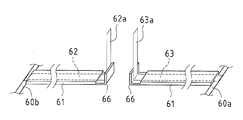
- FIG. 3 is a partially enlarged perspective view of the periphery of the output lead portions 62a and 63a.
- the lead wire on the tip end side including the bent portion 66 is in the state of single-sided coating with the insulating film 61. More specifically, the insulating film 61 of this portion is provided on the back electrode film side of the solar cell string 56 of the lead wires 62a and 63a. That is, when the root portion is bent to vertically raise the output lead portions 62a and 63a, the insulating film 61 is provided only on one side of each of the lead wires 62 and 63 in this portion. Because it is weak due to stiffness and rebound, it can be easily bent vertically.
- the positive electrode lead wire 62 and the negative electrode lead wire 63 are made of the same material (i.e., copper foil) as the positive electrode current collector portion 60a and the negative electrode current collector portion 60b, and as a bonding means between each lead wire and the current collector portion Soldering or spot welding can be used.
- the positive electrode lead wire 62 and the negative electrode lead wire 63 extend over the plurality of solar battery cells 55, but since the lead wires 62 and 63 are entirely covered with the insulating film 61, the plurality of solar battery cells There is no need to short 55.
- the sealing insulation is performed in a state where the output lead portions 62a and 63a of the positive electrode lead wire 62 and the negative electrode lead wire 63 are respectively inserted into the openings 64a and 64a and the openings 65a and 65a.
- a film 64 and a back film 65 as a back surface protection sheet for weather resistance and high insulation are laminated and sealed on the entire surface of the solar cell string 56.
- the sealing insulating film 64 may be made of PVB, silicone, etc., as long as it has good adhesion to the back film 65, the insulating film 61, and the solar battery cells 55 and is excellent in long-term weather resistance. Products made of acetate resin are most suitable because they have a track record for solar cells.
- the waterproof property of the solar cell string can be improved by selecting the sealing insulating film 64 and the insulating film 61 having good adhesion to each other.
- the back film 65 preferably has a three-layer structure including a moisture-proof layer such as PET / Al / PET (PET: polyethylene terephthalate).
- PET polyethylene terephthalate
- the back film 65 is set to 100 ⁇ m while the insulating film 61 is set to 50 ⁇ m and the sealing insulating film 64 is set to 600 ⁇ m.
- a terminal box not shown is attached and electrically connected.
- the electrode arrangement structure of the solar cell string 56 is merely an example, and the invention is not limited to such an arrangement structure.
- the arrangement positions of the positive electrode lead wire 62 and the negative electrode lead wire 63 may be close to one end side of the solar cell string 56 instead of the central portion, and it is not necessary to pull out to the central portion. That is, the output lead portions 62a and 63a may be disposed so as to project upward from the vicinity of the positive electrode current collecting portion 60a and the negative electrode current collecting portion 60b.
- each lead wire 62, 63 is covered with the insulating film 61 on the entire surface from the current collecting portion 60a, 60b to the front of the bent portion 66, and includes the bent portion 66.
- the output lead portions 62a and 63a on the tip end side are coated on one side with the insulating film 61, but in the present configuration example 2, as shown in FIG. 4, the output lead portions 62a and 63a from the respective current collectors 60a and 60b.
- the entire up to the tip end side including the bent portion 66 is coated on one side with the insulating film 61.
- the insulating film 61 is provided on the back electrode film side of the solar cell string 56 of each of the lead wires 62 and 63. That is, when the root portion is bent to vertically raise the output lead portions 62a and 63a, the insulating film 61 is provided only on one side of each of the lead wires 62 and 63 in this portion. Because it is weak due to stiffness and rebound, it can be easily bent vertically. Further, by providing the insulating film 61 only on one side over the entire length of each of the lead wires 62 and 63 as described above, the amount of the insulating film used can be minimized and the parts cost can be reduced. .
- the insulating sheet is provided between the back electrode film of the solar cell 55 and the back film 65 so as to cover the entire periphery of the edge 65 a of the back film 65.
- a dielectric breakdown voltage between the end face of the Al layer exposed to the end face of the opening 65 a of the back film 65 and the back electrode film is secured. That is, in the method of manufacturing a solar cell module according to the present embodiment, solar cell 55 formed of a transparent electrode film, a photoelectric conversion layer, and a back electrode film is stacked on translucent insulating substrate 51.
- the insulating sheet may be disposed along at least the entire periphery of the opening 65 a of the back film 65.
- the opening 65a is rectangular
- the insulating sheet is, for example, in the form of an elongated tape (rectangular)
- a tape may be formed along each edge of the rectangular opening 65a.
- Four insulating sheets may be arranged to form four sides of a square.
- specific examples of the shape and arrangement of the insulating sheet will be described.
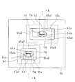
- FIG. 5 is a plan view of the vicinity of the opening showing the shape and arrangement of the insulating sheet of this specific example 1
- FIG. 6 is a cross-sectional view (accurately an end view) along the line AA of FIG.
- two openings 65a are formed corresponding to the output leads 62a and 63a of the respective lead wires 62 and 63, the shape and arrangement of the insulating sheet are the same for each opening 65a, so Now, one opening (the opening 65a on the right side in FIG. 6) will be described.
- the insulating sheet includes one rectangular insulating sheet 11a disposed along the edge 65a1 of one side of the opening 65a across which the lead wire 63 crosses, and three other non-crossing leads 63. It consists of another insulating sheet 11b disposed in a U-shape along the side edge portions 65a2 to 65a4.
- the insulating sheet 11 a is disposed between the lead wire 63 and the sealing insulating film (for example, an EVA sheet) 64, and the insulating sheet 11 b is disposed between the sealing insulating film 64 and the back film 65. There is. That is, the insulating sheet 11 a is disposed below the sealing insulating film 64, and the insulating sheet 11 b is disposed above the sealing insulating film 64.
- the sealing insulating film for example, an EVA sheet
- the insulating sheet 11a is a pressure-sensitive adhesive sheet whose lower surface is coated with a pressure-sensitive adhesive, and is disposed along the edge 65a1 of the opening 65a of the back film 65 on the back surface electrode film of the solar battery cell 55.
- the lead wires 63 are fixed or temporarily fixed on the EVA sheet 59. That is, the insulating sheet 11 a serves as both the insulation of the edge 65 a 1 of the opening 65 a and the fixation of the lead wire 63. Thus, during the subsequent laminating process, the insulating sheet 11a is prevented from shifting from the edge 65a1 of the opening 65a, and also serves to fix or temporarily fix the arrangement position of the lead wire 63 not to shift. There is. That is, the lead wire 63 can be reliably disposed and fixed at a position not in contact with the end face of the opening 65 a of the back film 65.
- the insulating sheet 11b is disposed along the edges 65a2 to 65a4 of the other three sides of the opening 65a of the back film 65, and is fixed or temporarily fixed to the lower surface of the edges 65a2 to 65a4. . This prevents the insulating sheet 11b from shifting from the edge portions 65a2 to 65a4 of the three sides of the opening 65a in the subsequent lamination process.
- the entire circumference of the edge of the opening 65 a of the back film 65 is completely covered between the back electrode film of the solar battery cell 55 and the back film 65.
- the insulating sheets 11a and 11b are reliably disposed.
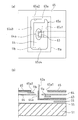
- FIGS. 7 (a) and 7 (b) are a plan view and a cross-sectional view (precisely an end view) of the vicinity of the opening showing the shape and arrangement of the insulating sheet of this specific example 2.
- FIG. 7 has shown the case where it applies to the solar cell module of the structure shown in FIG. 3 (namely, the solar cell module in which the lead wires 62 and 63 are double coated).
- FIG. 7 only one opening 65 a and one opening 65 a from which the output lead portion 63 a of one lead wire 63 is derived are illustrated, but the other output lead 62 a is extracted
- the opening 65a of the same has the same structure.
- the difference between this example 2 and the above example 1 is that the above example 1 arranges the EVA sheet 59 on the entire back electrode film of the solar battery cell 55, while this example 2
- the sheet 59 is disposed only to the front of the opening 65 a of the back film 65, and the other configuration is the same as that of the first example. Therefore, in this case, when arranging the rectangular insulating sheet 11a on the back surface electrode film of the solar battery cell 55 along the edge 65a1 of the opening 65a of the back film 65, the lead wire 63 is back surface electrode It will be fixed directly or temporarily fixed on the membrane.
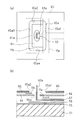
- FIGS. 8 (a) and 8 (b) are a plan view and a cross-sectional view (precisely an end view) of the vicinity of the opening showing the shape and arrangement of the insulating sheet of this specific example 3.
- FIG. 8 has shown the case where it applies to the solar cell module of the structure shown in FIG. 3 (that is, the solar cell module in which the lead wires 62 and 63 are double coated).
- FIG. 8 only one opening 65 a and one opening 65 a from which the output lead portion 63 a of one lead wire 63 is derived are illustrated, but the other output lead 62 a is The opening 65a of the same has the same structure.
- the sealing insulating film 64 is formed to have the same size as the back film 65 in the above specific example 1, while this sealing in the present specific example 3
- a lead wire adhesive sheet small piece 641 having a width slightly larger than the width of the opening 65a of the back film 65 is disposed along the lead wire 63. It is almost the same as Therefore, in this case, the lead wire 63 is fixed or temporarily fixed on the EVA sheet 59 by the rectangular insulating sheet 11 a and the lead wire adhesive sheet small piece 641.
- the lead wires 63 can be fixed or temporarily fixed on the EVA sheet 59 by the lead wire adhesive sheet pieces 641, the insulating sheet 11 a is attached to the edge 65 a 1 of one side of the opening 65 a of the back film 65. It may be configured to be fixed or temporarily fixed to the lower surface of the lead wire adhesive sheet small piece 641 arranged up to the edge 65a1 of one side of the opening 65 in a state of being arranged along.
- FIGS. 9 (a) and 9 (b) are a plan view and a cross-sectional view (precisely an end view) of the periphery of the opening showing the shape and arrangement of the insulating sheet of the fourth specific example.
- FIG. 9 has shown the case where it applies to the solar cell module of the structure shown in FIG. 3 (namely, the solar cell module in which the lead wires 62 and 63 are double coated).
- FIG. 9 only one opening 65a and one opening 65a from which the output lead portion 63a of one lead wire 63 is led out are shown, but the other output lead 62a is The opening 65a of the same has the same structure.
- the difference between this example 4 and the above example 1 is that the above example 1 arranges the EVA sheet 59 on the entire back electrode film of the solar battery cell 55 while this example 4 The point that the sheet 59 is disposed only up to the opposing edge of the opening 65a of the back film 65, and the example 1 is the same as the opening 64a of the sealing insulating film 64 and the opening 65a of the back film 65.
- the opening 64a of the sealing insulating film 64 is smaller than the opening 65a of the back film 65 while the opening of the size is taken as an example.
- the sealing insulating film 64 is extended to the inside of the opening 65 a of the back film 65.
- the lead wire 63 is EVA sheet It will fix or temporarily fix on 59.
- the insulating sheet 11 a is disposed on the lower surface of the sealing insulating film 64 extended in the opening 65 with an adhesive in a state where the insulating sheet 11 a is disposed along the edge 65 a 1 of one side of the opening 65 a of the back film 65. It may be fixed or temporarily fixed.
- FIGS. 10 (a) and 10 (b) are a plan view and a cross-sectional view (precisely an end view) of the vicinity of the opening showing the shape and arrangement of the insulating sheet of this specific example 5.
- FIG. 10 has shown the case where it applies to the solar cell module of the structure shown in FIG. 3 (that is, the solar cell module in which the lead wires 62 and 63 are double coated).
- FIG. 10 only the one opening 65a and the one opening 65a from which the output lead portion 63a of one lead wire 63 is derived are illustrated, but the other output lead 62a is derived from the other
- the opening 65a of the same has the same structure.
- the insulating sheet 11c is formed in a shape that forms four sides of a square in plan view so as to cover the edge along the entire periphery of the opening 65a of the back film 65. It consists of a sheet of sheets. And the insulating sheet 11c of such a shape is arrange
- Insulating sheet 11c is a pressure-sensitive adhesive sheet whose lower surface is coated with a pressure-sensitive adhesive, and the back electrode film of solar battery cell 55 along the entire circumference of edge portions 65a1 to 65a4 of opening 65a of back film 65.
- the lead wires 63 are fixed on the back surface electrode film (more precisely, on the EVA sheet 59) by the insulating sheet 11c. That is, the insulating sheet 11c serves both to insulate all the edge portions 65a1 to 65a4 of the opening 65a and to fix the lead wire 63.
- the insulating sheet 11c is prevented from shifting from the entire edge 65a1 to 65a4 of the opening 65a, and is fixed or temporarily fixed so that the arrangement position of the lead wire 63 is not shifted. It also plays a role.
- the adhesive applied to the lower surface of the insulating sheet 11c may be applied only to one side facing the edge 65a1 of one side of the opening 65a across which the lead wire 63 crosses.
- the whole is laminated to form the opening 65a of the back film 65 between the back electrode film of the solar battery cell 55 and the back film 65.
- the insulating sheet 11c is disposed so as to completely cover the entire circumference of the edge of the.
- FIG. 11 is a cross-sectional view (precisely an end view) of the vicinity of the opening showing the shape and arrangement of the insulating sheet of the present specific example 6. Note that the plan view is the same as FIG.
- the insulating sheet 11d is formed in a shape that forms four sides of a square in plan view so as to cover the edge along the entire periphery of the opening 65a of the back film 65. It consists of one sheet. Then, the insulating sheet 11 d having such a shape is disposed between the back film 65 and the sealing insulating film 64.
- the insulating sheet 11d is coated with an adhesive on the outer periphery of the upper surface, and when the insulating sheet 11d is arranged along the entire periphery of the edge portions 65a1 to 65a4 of the opening 65a of the back film 65, the back film
- the insulating sheet 11 d is fixed or temporarily fixed to the lower surface of the back film 65 by aligning the position from the lower surface side of the opening 65 a 65 and attaching it. This prevents the insulating sheet 11d from shifting from the entire peripheral edge portions 65a1 to 65a4 of the opening 65a in the subsequent laminating process.
- the whole is laminated to completely cover the entire periphery of the opening 65 a of the back film 65 between the back surface electrode film of the solar battery cell 55 and the back film 65, and the insulating sheet 11d will be placed.
- FIG. 12 has shown the case where it applies to the solar cell module of the structure shown in FIG. 3 (that is, the solar cell module in which the lead wires 62 and 63 have a double-sided coating).
- FIG. 12 only one opening 65a and one opening 65a from which the output lead portion 63a of one lead wire 63 is led out are shown, but the other output lead 62a is The opening 65a of the same has the same structure.
- the insulating sheet 11e is formed as a single sheet of a size (shown by a two-dot chain line in FIG. 12A) covering the entire opening 65a of the back film 65, and the solar battery cell Arranged between the back surface electrode film of 55 and the lead wire 63 (more precisely, arranged between the EVA sheet 59 for adhesion and the lead wire 63 arranged on the back surface electrode film of the solar battery cell 55) It is done. Then, one edge 11e1 (the edge on the right side in the figure) of the insulating sheet 11e is disposed so as to overlap the end 611 of the insulating film 61 disposed on the lower surface side of the lead wire 63. The other edge (left edge in the figure) 11e2 is bonded or affixed to the lower surface of one edge 65a3 of the opening 65a of the back film 65 through the opening 64a of the sealing insulating film 64.
- the coating on the lower surface side of the lead wire 63 is the insulating sheet It is sufficient to partially overlap the edge 11e1 of 11e, and it is not necessary to cover the lead wire 63 with the insulating film 61 as shown in FIG. Therefore, when the lead wire 63 is bent so as to rise from the opening 65a of the back film 65, since the insulating film 61 is not at the bent portion, the lead wire 63 may be easily bent at an arbitrary angle desired by the user. it can.
- FIGS. 13 (a) and 13 (b) are a plan view and a cross-sectional view (precisely an end view) of the vicinity of the opening showing the shape and arrangement of the insulating sheet of Concrete Example 8.
- FIG. 13 has shown the case where it applies to the solar cell module of the structure shown in FIG. 4 (namely, the solar cell module in which the lead wires 62 and 63 are coated on one side).
- FIG. 13 only one opening 65 a and one opening 65 a from which the output lead portion 63 a of one lead wire 63 is derived are illustrated, but the other output lead 62 a is drawn out
- the opening 65a of the same has the same structure.
- the insulating sheet 11f is formed as a single sheet of a size (shown by a two-dot chain line in FIG. 13A) covering the entire opening 65a of the back film 65, and the lower surface side is insulating It is disposed between the lead wire 63 covered with the film 61 and the upper surface side exposed and the sealing insulating film 64.
- the lead wire 63 passes under the insulating sheet 11f disposed under the opening 65a of the back film 65 and is pulled out to the end (left end in FIG. 13B) 11f1 of the insulating sheet 11f.
- the coating of the lead wire 63 with the insulating film 61 may be coated on one side with the back electrode film of the solar battery cell 55, and the coating of the other surface of the bent portion of the lead 63 is unnecessary. It becomes. Therefore, the bending process of the lead wire 63 becomes easy in the state where the insulation state by the insulating sheet 11 f is maintained.
- FIGS. 14 (a) and 14 (b) are a plan view and a cross-sectional view (precisely an end view) of the vicinity of the opening showing the shape and arrangement of the insulating sheet of this example 9.
- FIG. 14 has shown the case where it applies to the solar cell module of the structure shown in FIG. 4 (namely, the solar cell module in which the lead wires 62 and 63 are coated on one side).
- FIG. 14 only one opening 65 a and one opening 65 a from which the output lead portion 63 a of one lead wire 63 is derived are illustrated, but the other output lead 62 a is derived from the other
- the opening 65a of the same has the same structure.
- the configuration of this example 9 is substantially the same as the configuration of the above example 8, except that the end 11f2 opposite to the end 11f1 of the insulating sheet 11f in which the lead wire 63 is folded back is sealed It is a point fixed or temporarily fixed to the lower surface of the opening 65a of the back film 65 through the opening 64a of the insulating film 64 with an adhesive or the like.
- the insulating sheet 11d does not deviate from the entire peripheral edge portions 65a1 to 65a4 of the opening 65a, so the Al layer end face exposed to the end face of the opening 65a of the back film 65 and the sun
- the back electrode film of the battery cell 55 can be reliably insulated.
- FIGS. 15 (a) and 15 (b) are a plan view and a cross-sectional view (precisely an end view) of the vicinity of the opening showing the shape and arrangement of the insulating sheet of this specific example 10.
- FIG. 15 has shown the case where it applies to the solar cell module of the structure shown in FIG. 3 (that is, the solar cell module in which the lead wires 62 and 63 are double coated).
- FIG. 15 only one opening 65a and one opening 65a from which the output lead portion 63a of one lead wire 63 is drawn are illustrated, but the other output lead 62a is The opening 65a of the same has the same structure.
- the insulating sheet 11g directly covers the end face of the opening 65a of the back film 65 over the entire circumference. More specifically, the insulating sheet 11g is formed in a frame shape in plan view so as to cover the lower surface and the upper surface of the edge of the opening 65a and the end surface of the opening 65a over the entire circumference. It is formed in a substantially U-shape. In particular, in order to secure the withstand voltage between the Al layer end face of the end face of the opening 65a and the back electrode film of the solar battery cell 55, it is important to cover the lower surface of the edge of the opening 65a with the insulating sheet 11g is there.
- the discharge between the Al layer end face exposed to the end face of the opening 65a and the back surface electrode film of the solar battery cell 55 is reliably prevented. be able to. Therefore, even if the withstand voltage test at a high voltage corresponding to a high voltage solar cell module is performed, a sufficient withstand voltage can be obtained without discharging.
- FIG. 16 has shown the case where it applies to the solar cell module of the structure shown in FIG. 3 (ie, the solar cell module in which the lead wires 62 and 63 are double-sided coatings).
- FIG. 16 only one opening 65 a and one opening 65 a from which the output lead portion 63 a of one lead wire 63 is derived are illustrated, but the other output lead 62 a is drawn out
- the opening 65a of the same has the same structure.
- the lower covering insulating film 61b of the lead wire 63 is used as an insulating sheet, instead of separately providing an insulating sheet covering the opening 65a of the back film 65. That is, the lower coating insulation film 61b of the lead wire 63 is formed to have a width slightly larger than the width of the opening 65a of the back film 65, and extended so as to exceed the edge 65a3 of the other side of the opening 65a. Are arranged. Thus, the edge portion of the opening 65a of the back film 65 can be covered over the entire circumference by the extended portion 61b1 of the lower covering insulating film 61b.
- FIGS. 17 (a) and 17 (b) are plan views around the opening showing the shape and arrangement of the insulating sheet of this specific example 12 (however, the back film 65 and the sealing insulating film 64 are not shown) And a cross-sectional view (precisely an end view).
- FIG. 17 has shown the case where it applies to the solar cell module of the structure shown in FIG. 3 (namely, the solar cell module in which the lead wires 62 and 63 are double coated).
- FIG. 17 shows only one opening 65a from which one output 65a and one output lead 63a of one lead wire 63 are drawn, but the other output lead 62a is drawn from the other
- the opening 65a of the same has the same structure.
- this example 12 differs from the example 11 in that in the example 11, only the lower covering insulating film 61b of the lead wire 63 is formed in a width slightly larger than the width of the opening 65a of the back film 65. Further, in the present specific example 12, the upper covering insulating film 61a is also formed to have a width slightly larger than the width of the opening 65a of the back film 65, and the edge 65a1 of one side of the opening 65a is exceeded to enter the opening 65a.
- the extended portion 61b1 of the lower cover insulating film 61b can cover the edge of the opening 65a of the back film 65 over the entire circumference, and the extended portion 61a1 of the upper cover insulating film 61a The edge 65a1 of one side of the opening 65a can be further covered.
- FIG. 18 is applied to the solar cell module having the configuration shown in FIG. 4 (ie, a single-sided coated solar cell module in which the lead wires 62 and 63 are coated only on the side close to the back electrode of the solar battery cell 55). It shows. In FIG. 18, only one opening 65 a and one opening 65 a from which the output lead portion 63 a of one lead wire 63 is derived are illustrated, but the other output lead 62 a is drawn out The opening 65a of the same has the same structure.
- the present example 13 is a modification of the above-mentioned example 11.
- the lead wire 63 is a single-sided coating coated only on the side close to the back electrode of the solar battery cell 55, the same procedure as in the above-mentioned example 1 is performed between the lead wire 63 and the back film 65. , And a rectangular insulating sheet 11h.
- the lower coating insulation film 61b of the lead wire 63 is formed to have a width slightly larger than the width of the opening 65a of the back film 65, and extended so as to exceed the edge 65a3 of the other side of the opening 65a. Are arranged.
- the edge portion of the opening 65a of the back film 65 can be covered over the entire circumference by the extended portion 61b1 of the lower covering insulating film 61b.
- the rectangular insulating sheet 11 h is disposed along the edge 65 a 1 of one side of the opening 65 a across which the lead wire 63 crosses.
- the insulating sheet 11 h is disposed between the lead wires 63 and a sealing insulating film (for example, an EVA sheet) 64, and is a pressure-sensitive adhesive sheet on the lower surface of which an adhesive is applied. Further, the insulating sheet 11h is formed to be wider than the width of the lower covering insulating film 61b. Then, when arranging the insulating sheet 11 h on the back surface electrode film of the solar battery cell 55 along the edge 65 a 1 of the opening 65 a of the back film 65, the lead wire 63 is fixed or temporarily fixed on the EVA sheet 59 It is supposed to be.
- a sealing insulating film for example, an EVA sheet
- the insulating sheet 11 h serves as both the insulation of the edge 65 a 1 of the opening 65 a and the fixation of the lead wire 63.
- the insulating sheet 11h is prevented from shifting from the edge 65a1 of the opening 65a, and also serves to fix or temporarily fix the arrangement position of the lead wire 63 not to shift.
- the lead wire 63 can be reliably disposed and fixed at a position not in contact with the end face of the opening 65 a of the back film 65.
- FIGS. 19 (a) and 19 (b) are plan views around the opening showing the shape and arrangement of the insulating sheet of the present specific example 14 (however, the back film 65 and the sealing insulating film 64 are not shown) And a cross-sectional view (precisely an end view).
- FIG. 19 is applied to the solar cell module having the configuration shown in FIG. 4 (ie, a single-sided coated solar cell module in which the lead wires 62 and 63 are coated only on the side close to the back electrode of the solar battery cell 55). It shows.
- FIG. 19 only one opening 65a and one opening 65a from which the output lead portion 63a of one lead wire 63 is derived are illustrated, but the other output lead 62a is derived from the other The opening 65a of the same has the same structure.
- the present example 14 is a modification of the example 13, and the rectangular insulating sheet 11i is shorter than the insulating sheet 11h of the example 13.
- the lower coating insulation film 61b of the lead wire 63 is formed to have a width slightly larger than the width of the opening 65a of the back film 65, and extended so as to exceed the edge 65a3 of the other side of the opening 65a. Are arranged.
- the edge portion of the opening 65a of the back film 65 can be covered over the entire circumference by the extended portion 61b1 of the lower covering insulating film 61b.
- the rectangular insulating sheet 11i is disposed along the edge 65a1 of one side of the opening 65a across which the lead wire 63 crosses.
- the insulating sheet 11i is disposed between the back film 65 and the sealing insulating film (for example, an EVA sheet) 64.
- the insulating sheet 11i is formed to have a width slightly larger than the width of the opening 65a of the back film 65, and to a width slightly smaller than the width of the lower covering insulating film 61b.
- the edge 65a1 lower surface of one side of the opening 65a of the back film 65 Is fixed or temporarily fixed by an adhesive. This prevents the insulating sheet 11i from shifting from the edge 65a1 of the opening 65a in the subsequent laminating process.
- FIGS. 20 (a) and 20 (b) are plan views around the opening showing the shape and arrangement of the insulating sheet of this specific example 15 (however, the back film 65 and the sealing insulating film 64 are not shown) And a cross-sectional view (precisely an end view).
- FIG. 20 shows a case where the present invention is applied to a non-insulated lead wire in which the lead wires 62 and 63 are not covered at all.
- FIG. 20 only one opening 65a and one opening 65a from which the output lead portion 63a of one lead wire 63 is drawn are illustrated, but the other output lead 62a is The opening 65a of the same has the same structure.
- an insulating layer (insulating film) 68 for covering the lower side of the lead wire 63 is provided on the back surface electrode film of the solar battery cell 55.
- the insulating layer 68 is formed to have a width slightly larger than the width of the opening 65a of the back film 65, and is disposed along the lead wire 63 to a position beyond the edge 65a3 of the other side of the opening 65a. It is. Thereby, the edge of the opening 65 a of the back film 65 can be covered by the insulating layer 68 over the entire circumference.
- the lead wire 63 since the lead wire 63 is in a non-insulated state (a bare state not covered at all), the edge of one side of the opening 65a where the lead wire 63 intersects the rectangular insulating sheet 11j. It is arranged along 65a1.
- the insulating sheet 11 j is disposed between the lead wires 63 and a sealing insulating film (for example, an EVA sheet) 64, and is a pressure-sensitive adhesive sheet on the lower surface of which an adhesive is applied. Then, when arranging the insulating sheet 11 j on the back surface electrode film of the solar cell 55 along the edge 65 a 1 of the opening 65 a of the back film 65, the lead wire 63 is fixed or temporarily fixed on the insulating layer 68 It is supposed to be.
- a sealing insulating film for example, an EVA sheet
- the insulating sheet 11 j serves as both the insulation of the edge 65 a 1 of the opening 65 a and the fixation of the lead wire 63.
- the insulating sheet 11 j is prevented from shifting from the edge 65 a 1 of the opening 65 a at the time of subsequent lamination processing, and also serves to fix or temporarily fix the arrangement position of the lead wire 63 not to shift.
- the lead wire 63 can be reliably disposed and fixed at a position not in contact with the end face of the opening 65 a of the back film 65.
- FIGS. 21 (a) and 21 (b) are plan views around the opening showing the shape and arrangement of the insulating sheet of this specific example 16 (however, the back film 65 and the sealing insulating film 64 are not shown) And a cross-sectional view (precisely an end view).
- FIG. 21 shows a case where the present invention is applied to a non-insulated lead wire in which the lead wires 62 and 63 are not covered at all.
- FIG. 21 only one opening 65a and one opening 65a from which the output lead portion 63a of one lead wire 63 is derived are illustrated, but the other output lead 62a is derived from the other
- the opening 65a of the same has the same structure.
- the present example 16 is a modification of the example 15, and the width of the rectangular insulating sheet 11k is made shorter than the width of the insulating sheet 11j of the example 15 to cover only the lead wire 63. It is something like that.
- the insulating sheet 11k is a pressure-sensitive adhesive sheet whose lower surface is coated with a pressure-sensitive adhesive, and the solar cell 55 is placed along the edge 65a1 of the opening 65a of the back film 65.
- the lead wire 63 is fixed or temporarily fixed on the insulating layer 68 when it is disposed on the back electrode film.
- the other configuration is the same as that of the fifth specific example shown in FIG. 21, so the description is omitted here.
- FIG. 22 shows a case where the present invention is applied to a non-insulated lead wire in which the lead wires 62 and 63 are not covered at all.
- FIG. 22 only one opening 65a and one opening 65a from which the output lead portion 63a of one lead wire 63 is led out are shown, but the other output lead 62a is The opening 65a of the same has the same structure.
- the present example 17 is a modified example of the above-mentioned example 15, in which the rectangular insulating sheet 11m is disposed between the back film 65 and the sealing insulating film 64.
- the insulating sheet 11 m is disposed along the edge 65 a 1 of one side of the opening 65 a across which the lead wire 63 crosses.
- the insulating sheet 11m is disposed between the back film 65 and the sealing insulating film (for example, an EVA sheet) 64.
- the insulating sheet 11i is formed to have a width slightly larger than the width of the opening 65a of the back film 65, and to a width slightly smaller than the width of the insulating layer 68.
- the edge 65 a 1 lower surface of one side of the opening 65 a of the back film 65 Is fixed or temporarily fixed by an adhesive. This prevents the insulating sheet 11m from shifting from the edge 65a1 of the opening 65a in the subsequent laminating process.
- the case where one lead wire is led out from one opening 65a of the back film 65 is described, but both lead wires 62, 63 are led out from one opening 65a. You may do so.
- the insulating sheet having the same shape can be applied to the specific examples 2, 3, 5, and 7.
- the other edge of the insulating sheet 11e bonded or fixed to the lower surface of one edge of the opening 65a of the back film 65 is, for example, as shown in FIG.
- the upper edge 65a2 or the lower edge 65a4 of 14 (a) can be applied as it is. That is, the other edge of the insulating sheet 11e bonded or fixed to the lower surface of one edge of the opening 65a of the back film 65 may be any edge not intersecting the lead wire.
- the same can be applied to the fourth and sixth specific examples.
- the solar cell module of the present invention and the method for manufacturing the same can reliably prevent the discharge between the back surface electrode film of the solar cell module and the opening end face of the back surface protection sheet, and thereby, the withstand voltage at high voltage Even if a test is conducted, a sufficient withstand voltage can be obtained without discharging, which is useful in that high voltage of the solar cell module can be achieved.
- Insulating Sheet 51 Translucent Insulating Substrate 55
- Solar Battery Cell 56
- Solar Cell String (Thin Film Solar Cell String) 57
- P-type electrode terminal portion 58
- N-type electrode terminal portion 59
- EVA sheet 60
- a positive electrode current collecting portion 60
- negative electrode current collecting portion 61
- insulating film (insulating film) 62
- positive electrode lead wire 63
- negative electrode lead wire 62a
Abstract
Description
特許文献2の薄膜太陽電池モジュールは、その図5(D)、図6(E)に示されているように、充填材のシートの上に保護カバーの穴より少し大きめで切り込みのあるTedlerシート小片を半田メッキ銅箔(上記構成の出力リード部122a,123a)の周りにセットし、さらにほぼ同じサイズのEVAシート小片12をセットしてから、裏面保護カバーをその上からセットする構造となっている。そして、裏面保護カバーの開口から半田メッキ銅箔を出すとともに耐熱性テープで銅箔と裏面保護カバーが接触しない位置に固定することにより、真空ラミネート工程でずれることなく、ショートしないようにすることが記載されている。
図1(a),(b)及び図2は、本実施の形態に係る太陽電池モジュールの構成例1を示している。ただし、図1(a),(b)は製造工程の2つの場面を示す説明図、図2は太陽電池ストリングをラミネート封止する工程を示す説明図である。
上記構成例1に示す太陽電池ストリングでは、各リード線62,63は、各集電部60a,60bから折り曲げ部66の手前までが絶縁フィルム61による全面被覆となっており、折り曲げ部66を含む先端部側の出力リード部62a,63aが絶縁フィルム61による片面被覆となっているが、本構成例2では、図4に示すように、各集電部60a,60bから出力リード部62a,63aの折り曲げ部66を含む先端部側までの全てが絶縁フィルム61による片面被覆となっている。より具体的には、この絶縁フィルム61は、各リード線62,63の太陽電池ストリング56の裏面電極膜側に設けられている。すなわち、出力リード部62a,63aを垂直に立ち上げるためにその根元部分を折り曲げるとき、この部分には各リード線62,63の片面のみにしか絶縁フィルム61が設けられていないので、絶縁フィルム61によるコシや跳ね返りが弱いため、容易に垂直に折り曲げることができる。また、このように各リード線62,63のほぼ全長にわたって絶縁フィルム61を片面のみに設けることにより、絶縁フィルムの使用量を必要最小限に抑えることができ、部品コストの低減につなげることができる。
本実施の形態では、上記構成の太陽電池モジュールにおいて、太陽電池セル55の裏面電極膜とバックフィルム65との間に、バックフィルム65の開口部65aの縁部全周を覆うように絶縁シートを配置することによって、バックフィルム65の開口部65a端面に露出したAl層の端面と裏面電極膜との間の絶縁耐圧を確保する構成としたものである。すなわち、本実施の形態の太陽電池モジュールの製造方法は、透光性絶縁基板51上に、透明電極膜、光電変換層、裏面電極膜からなる太陽電池セル55を積層し、この太陽電池セル55の裏面電極膜上に、絶縁状態のリード線62,63と、このリード線62,63の出力リード部62a,63aを導出するための開口部65aを有するバックフィルム65とを順次積層する工程において、前記裏面電極膜とバックフィルム65との間に、バックフィルム65の開口部65aの縁部全周を覆うように絶縁シートを配置する工程を含むものである。
図5は、本具体例1の絶縁シートの形状及び配置構成を示す開口部周辺の平面図、図6は、図5のA-A線に沿う断面図(正確には端面図)である。なお、開口部65aは各リード線62,63の出力リード部62a,63aに対応して2個形成されているが、絶縁シートの形状及び配置構成は各開口部65aで同じであるので、ここでは一方の開口部(図6中右側の開口部65a)について説明する。
図7(a),(b)は、本具体例2の絶縁シートの形状及び配置構成を示す開口部周辺の平面図及び断面図(正確には端面図)である。ただし、図7は、図3に示す構成の太陽電池モジュール(すなわち、リード線62,63が両面被覆の太陽電池モジュール)に適用した場合を示している。また、図7では、一方の開口部65aと一方のリード線63の出力リード部63aが導出される一方の開口部65aのみを図示しているが、他方の出力リード部62aが導出される他方の開口部65aも同じ構造である。
図8(a),(b)は、本具体例3の絶縁シートの形状及び配置構成を示す開口部周辺の平面図及び断面図(正確には端面図)である。ただし、図8は、図3に示す構成の太陽電池モジュール(すなわち、リード線62,63が両面被覆の太陽電池モジュール)に適用した場合を示している。また、図8では、一方の開口部65aと一方のリード線63の出力リード部63aが導出される一方の開口部65aのみを図示しているが、他方の出力リード部62aが導出される他方の開口部65aも同じ構造である。
図9(a),(b)は、本具体例4の絶縁シートの形状及び配置構成を示す開口部周辺の平面図及び断面図(正確には端面図)である。ただし、図9は、図3に示す構成の太陽電池モジュール(すなわち、リード線62,63が両面被覆の太陽電池モジュール)に適用した場合を示している。また、図9では、一方の開口部65aと一方のリード線63の出力リード部63aが導出される一方の開口部65aのみを図示しているが、他方の出力リード部62aが導出される他方の開口部65aも同じ構造である。
図10(a),(b)は、本具体例5の絶縁シートの形状及び配置構成を示す開口部周辺の平面図及び断面図(正確には端面図)である。ただし、図10は、図3に示す構成の太陽電池モジュール(すなわち、リード線62,63が両面被覆の太陽電池モジュール)に適用した場合を示している。また、図10では、一方の開口部65aと一方のリード線63の出力リード部63aが導出される一方の開口部65aのみを図示しているが、他方の出力リード部62aが導出される他方の開口部65aも同じ構造である。
図11は、本具体例6の絶縁シートの形状及び配置構成を示す開口部周辺の断面図(正確には端面図)である。なお、平面図は図10(a)と同じである。
図12(a),(b)は、本具体例7の絶縁シートの形状及び配置構成を示す開口部周辺の平面図及び断面図(正確には端面図)である。ただし、図12は、図3に示す構成の太陽電池モジュール(すなわち、リード線62,63が両面被覆の太陽電池モジュール)に適用した場合を示している。また、図12では、一方の開口部65aと一方のリード線63の出力リード部63aが導出される一方の開口部65aのみを図示しているが、他方の出力リード部62aが導出される他方の開口部65aも同じ構造である。
図13(a),(b)は、本具体例8の絶縁シートの形状及び配置構成を示す開口部周辺の平面図及び断面図(正確には端面図)である。ただし、図13は、図4に示す構成の太陽電池モジュール(すなわち、リード線62,63が片面被覆の太陽電池モジュール)に適用した場合を示している。また、図13では、一方の開口部65aと一方のリード線63の出力リード部63aが導出される一方の開口部65aのみを図示しているが、他方の出力リード部62aが導出される他方の開口部65aも同じ構造である。
図14(a),(b)は、本具体例9の絶縁シートの形状及び配置構成を示す開口部周辺の平面図及び断面図(正確には端面図)である。ただし、図14は、図4に示す構成の太陽電池モジュール(すなわち、リード線62,63が片面被覆の太陽電池モジュール)に適用した場合を示している。また、図14では、一方の開口部65aと一方のリード線63の出力リード部63aが導出される一方の開口部65aのみを図示しているが、他方の出力リード部62aが導出される他方の開口部65aも同じ構造である。
図15(a),(b)は、本具体例10の絶縁シートの形状及び配置構成を示す開口部周辺の平面図及び断面図(正確には端面図)である。ただし、図15は、図3に示す構成の太陽電池モジュール(すなわち、リード線62,63が両面被覆の太陽電池モジュール)に適用した場合を示している。また、図15では、一方の開口部65aと一方のリード線63の出力リード部63aが導出される一方の開口部65aのみを図示しているが、他方の出力リード部62aが導出される他方の開口部65aも同じ構造である。
図16(a),(b)は、本具体例11の絶縁シートの形状及び配置構成を示す開口部周辺の平面図(ただし、バックフィルム65と封止絶縁フィルム64は図示を省略している。)及び断面図(正確には端面図)である。ただし、図16は、図3に示す構成の太陽電池モジュール(すなわち、リード線62,63が両面被覆の太陽電池モジュール)に適用した場合を示している。また、図16では、一方の開口部65aと一方のリード線63の出力リード部63aが導出される一方の開口部65aのみを図示しているが、他方の出力リード部62aが導出される他方の開口部65aも同じ構造である。
図17(a),(b)は、本具体例12の絶縁シートの形状及び配置構成を示す開口部周辺の平面図(ただし、バックフィルム65と封止絶縁フィルム64は図示を省略している。)及び断面図(正確には端面図)である。ただし、図17は、図3に示す構成の太陽電池モジュール(すなわち、リード線62,63が両面被覆の太陽電池モジュール)に適用した場合を示している。また、図17では、一方の開口部65aと一方のリード線63の出力リード部63aが導出される一方の開口部65aのみを図示しているが、他方の出力リード部62aが導出される他方の開口部65aも同じ構造である。
図18(a),(b)は、本具体例13の絶縁シートの形状及び配置構成を示す開口部周辺の平面図(ただし、バックフィルム65と封止絶縁フィルム64は図示を省略している。)及び断面図(正確には端面図)である。ただし、図18は、図4に示す構成の太陽電池モジュール(すなわち、リード線62,63が太陽電池セル55の裏面電極に近い側のみ被覆された片面被覆の太陽電池モジュール)に適用した場合を示している。また、図18では、一方の開口部65aと一方のリード線63の出力リード部63aが導出される一方の開口部65aのみを図示しているが、他方の出力リード部62aが導出される他方の開口部65aも同じ構造である。
図19(a),(b)は、本具体例14の絶縁シートの形状及び配置構成を示す開口部周辺の平面図(ただし、バックフィルム65と封止絶縁フィルム64は図示を省略している。)及び断面図(正確には端面図)である。ただし、図19は、図4に示す構成の太陽電池モジュール(すなわち、リード線62,63が太陽電池セル55の裏面電極に近い側のみ被覆された片面被覆の太陽電池モジュール)に適用した場合を示している。また、図19では、一方の開口部65aと一方のリード線63の出力リード部63aが導出される一方の開口部65aのみを図示しているが、他方の出力リード部62aが導出される他方の開口部65aも同じ構造である。
図20(a),(b)は、本具体例15の絶縁シートの形状及び配置構成を示す開口部周辺の平面図(ただし、バックフィルム65と封止絶縁フィルム64は図示を省略している。)及び断面図(正確には端面図)である。ただし、図20は、リード線62,63が全く被覆されていない非絶縁状態のリード線に適用した場合を示している。また、図20では、一方の開口部65aと一方のリード線63の出力リード部63aが導出される一方の開口部65aのみを図示しているが、他方の出力リード部62aが導出される他方の開口部65aも同じ構造である。
図21(a),(b)は、本具体例16の絶縁シートの形状及び配置構成を示す開口部周辺の平面図(ただし、バックフィルム65と封止絶縁フィルム64は図示を省略している。)及び断面図(正確には端面図)である。ただし、図21は、リード線62,63が全く被覆されていない非絶縁状態のリード線に適用した場合を示している。また、図21では、一方の開口部65aと一方のリード線63の出力リード部63aが導出される一方の開口部65aのみを図示しているが、他方の出力リード部62aが導出される他方の開口部65aも同じ構造である。
図22(a),(b)は、本具体例17の絶縁シートの形状及び配置構成を示す開口部周辺の平面図(ただし、バックフィルム65と封止絶縁フィルム64は図示を省略している。)及び断面図(正確には端面図)である。ただし、図22は、リード線62,63が全く被覆されていない非絶縁状態のリード線に適用した場合を示している。また、図22では、一方の開口部65aと一方のリード線63の出力リード部63aが導出される一方の開口部65aのみを図示しているが、他方の出力リード部62aが導出される他方の開口部65aも同じ構造である。
51 透光性絶縁基板
55 太陽電池セル
56 太陽電池ストリング(薄膜太陽電池ストリング)
57 P型電極端子部
58 N型電極端子部
59 EVAシート
60a 正極集電部
60b 負極集電部
61 絶縁膜(絶縁フィルム)
62 正極リード線
63 負極リード線
62a,63a 出力リード部
64 封止絶縁フィルム
65 バックフィルム
64a,65a 開口部
Claims (17)
- 透光性絶縁基板上に、透明電極膜、光電変換層、裏面電極膜からなる太陽電池セルが積層され、この太陽電池セルの裏面電極膜上に、絶縁状態のリード線と、このリード線の出力リード部を導出するための開口部を有する裏面保護シートとが順次積層された太陽電池モジュールにおいて、
前記裏面電極膜と前記裏面保護シートとの間に、前記裏面保護シート開口部の縁部全周を覆うように絶縁シートが配置されていることを特徴とする太陽電池モジュール。 - 請求項1に記載の太陽電池モジュールにおいて、
前記絶縁シートは、前記リード線と前記裏面保護シートとの間に配置され、前記絶縁シート下面の粘着材によって前記リード線が前記裏面電極膜上に固定されることを特徴とする太陽電池モジュール。 - 請求項1または請求項2に記載の太陽電池モジュールにおいて、
前記裏面保護シートと前記裏面電極膜とは樹脂シートを用いて貼り合せており、
前記絶縁シートは、前記リード線と前記裏面保護シートとの間に配置され、前記絶縁シート下面の粘着材によって前記リード線が前記樹脂シート上に固定されることを特徴とする太陽電池モジュール。 - 請求項1または請求項2に記載の太陽電池モジュールにおいて、
前記リード線と前記裏面電極膜とは樹脂シートを用いて貼り合せており、
前記絶縁シートは、前記リード線と前記裏面保護シートとの間に配置され、前記絶縁シート下面の粘着材によって前記リード線が前記樹脂シート上に固定されることを特徴とする太陽電池モジュール。 - 請求項1に記載の太陽電池モジュールにおいて、
前記絶縁シートは、前記裏面保護シートの開口部全体を覆う大きさに形成されているとともに、前記裏面電極膜と前記リード線との間に配置され、前記絶縁シートの一方の縁部が前記リード線の下面側に配置されている絶縁フィルムの端部に重ねて配置され、他方の縁部が前記開口部の他方の縁部下面に接着または貼り付け固定されていることを特徴とする太陽電池モジュール。 - 請求項1に記載の太陽電池モジュールにおいて、
前記絶縁シートは、前記裏面保護シートの開口部全体を覆う大きさに形成されるとともに、下面側が絶縁フィルムで被覆され上面側が露出した状態の前記リード線と前記裏面保護シートとの間に配置され、前記リード線は、前記絶縁シートの端部を挟むように2つ折りに折り返した後、前記裏面保護シートの開口部から上方に導出されていることを特徴とする太陽電池モジュール。 - 請求項6に記載の太陽電池モジュールにおいて、
前記絶縁シートは、前記リード線で挟まれた端部とは別のいずれかの端部が前記開口部の縁部下面に接着または貼り付け固定されていることを特徴とする太陽電池モジュール。 - 請求項1に記載の太陽電池モジュールにおいて、
前記絶縁シートは、前記裏面保護シートの開口部端面を全周にわたって被覆するように配置されていることを特徴とする太陽電池モジュール。 - 請求項1に記載の太陽電池モジュールにおいて、
前記絶縁シートは、前記開口部の縁部下面及び上面と開口部端面とを全周にわたって被覆するように配置されていることを特徴とする太陽電池モジュール。 - 請求項1に記載の太陽電池モジュールにおいて、
前記絶縁シートは、リード線を被覆する絶縁フィルムの一部であることを特徴とする太陽電池モジュール。 - 請求項9に記載の太陽電池モジュールにおいて、
被覆リード線は裏面電極膜に近い側のみを被覆した片面被覆リード線であり、リード線と裏面保護シートの開口部とを、リード線とは別の絶縁シート小片で絶縁することを特徴とする太陽電池モジュール。 - 透光性絶縁基板上に、透明電極膜、光電変換層、裏面電極膜からなる太陽電池セルが積層され、この太陽電池セルの裏面電極膜上に、非絶縁状態のリード線と、このリード線の出力リード部を導出するための開口部を有する裏面保護シートとが順次積層された太陽電池モジュールにおいて、
前記裏面電極膜と前記裏面保護シートとの間に、前記裏面保護シートの開口部を縁部全周に沿って覆うように絶縁膜が形成されていることを特徴とする太陽電池モジュール。 - 請求項12に記載の太陽電池モジュールにおいて、
リード線と裏面保護シートの開口部とを、リード線とは別の絶縁シート小片で絶縁することを特徴とする太陽電池モジュール。 - 請求項11または請求項13に記載の太陽電池モジュールにおいて、
リード線と裏面保護シートの開口部との絶縁を確保する絶縁シート小片が、リード線を裏面電極膜に貼り付けて固定する固定テープを兼ねていることを特徴とする太陽電池モジュール。 - 請求項11または請求項13に記載の太陽電池モジュールにおいて、
リード線と裏面保護シートの開口部との絶縁を確保する絶縁シート小片が、裏面保護シートに貼り付けられていることを特徴とする太陽電池モジュール。 - 請求項12に記載の太陽電池モジュールにおいて、
リード線と裏面保護シートの開口部とを、リード線を部分的に絶縁フィルムで被覆することによって絶縁することを特徴とする太陽電池モジュール。 - 透光性絶縁基板上に、透明電極膜、光電変換層、裏面電極膜からなる太陽電池セルを積層し、この太陽電池セルの裏面電極膜上に、絶縁状態のリード線と、このリード線の出力リード部を導出するための開口部を有する裏面保護シートとを順次積層する太陽電池モジュールの製造方法において、
前記裏面電極膜と前記裏面保護シートとの間に、前記裏面保護シート開口部の縁部全周を覆うように絶縁シートを配置する工程を含むことを特徴とする太陽電池モジュールの製造方法。
Priority Applications (3)
| Application Number | Priority Date | Filing Date | Title |
|---|---|---|---|
| EP09829092A EP2360737A4 (en) | 2008-11-28 | 2009-11-25 | SOLAR BATTERY MODULE AND MANUFACTURING METHOD THEREFOR |
| US13/131,973 US8921684B2 (en) | 2008-11-28 | 2009-11-25 | Solar cell module and manufacturing method thereof |
| CN200980147822.XA CN102227821A (zh) | 2008-11-28 | 2009-11-25 | 太阳能电池模块及其制造方法 |
Applications Claiming Priority (2)
| Application Number | Priority Date | Filing Date | Title |
|---|---|---|---|
| JP2008304357A JP5268596B2 (ja) | 2008-11-28 | 2008-11-28 | 太陽電池モジュール及びその製造方法 |
| JP2008-304357 | 2008-11-28 |
Publications (1)
| Publication Number | Publication Date |
|---|---|
| WO2010061844A1 true WO2010061844A1 (ja) | 2010-06-03 |
Family
ID=42225717
Family Applications (1)
| Application Number | Title | Priority Date | Filing Date |
|---|---|---|---|
| PCT/JP2009/069846 WO2010061844A1 (ja) | 2008-11-28 | 2009-11-25 | 太陽電池モジュール及びその製造方法 |
Country Status (5)
| Country | Link |
|---|---|
| US (1) | US8921684B2 (ja) |
| EP (1) | EP2360737A4 (ja) |
| JP (1) | JP5268596B2 (ja) |
| CN (1) | CN102227821A (ja) |
| WO (1) | WO2010061844A1 (ja) |
Cited By (2)
| Publication number | Priority date | Publication date | Assignee | Title |
|---|---|---|---|---|
| WO2012030758A1 (en) * | 2010-08-30 | 2012-03-08 | First Solar, Inc. | Photovoltaic module cover |
| CN114744080A (zh) * | 2022-06-10 | 2022-07-12 | 苏州小牛自动化设备有限公司 | 一种电池串生产方法及电池串铺设设备 |
Families Citing this family (12)
| Publication number | Priority date | Publication date | Assignee | Title |
|---|---|---|---|---|
| WO2013031199A1 (ja) * | 2011-08-30 | 2013-03-07 | 三洋電機株式会社 | 太陽電池モジュール |
| EP2795678A1 (de) * | 2011-12-20 | 2014-10-29 | Saint-Gobain Glass France | Solarmodul mit abdichtelement |
| WO2013144095A1 (de) * | 2012-03-27 | 2013-10-03 | Bayer Intellectual Property Gmbh | Verwendung von uv-strahlenhärtbaren polyurethanharzen zur herstellung von solarlaminaten |
| JP2012142637A (ja) * | 2012-04-27 | 2012-07-26 | Sharp Corp | 太陽電池モジュール |
| US9331631B2 (en) | 2012-08-31 | 2016-05-03 | First Solar, Inc. | Direct connection of lead bar to conductive ribbon in a thin film photovoltaic device |
| US8722450B1 (en) * | 2013-03-18 | 2014-05-13 | Perfect Source Technology Corp. | Method for manufacturing improved solar cell module |
| JP6180842B2 (ja) * | 2013-07-30 | 2017-08-16 | ソーラーフロンティア株式会社 | 薄膜太陽電池モジュールの製造方法 |
| CN103687276A (zh) * | 2013-11-04 | 2014-03-26 | 成都聚合科技有限公司 | 一种大电流聚光光伏光电转换接收器 |
| WO2016051630A1 (ja) * | 2014-09-30 | 2016-04-07 | パナソニックIpマネジメント株式会社 | 太陽電池モジュールおよび太陽電池モジュールの製造方法 |
| US9899546B2 (en) | 2014-12-05 | 2018-02-20 | Tesla, Inc. | Photovoltaic cells with electrodes adapted to house conductive paste |
| US10043937B2 (en) | 2014-12-05 | 2018-08-07 | Solarcity Corporation | Systems and method for precision automated placement of backsheet on PV modules |
| FR3062594B1 (fr) * | 2017-02-03 | 2019-03-22 | Saint-Gobain Glass France | Vitrage feuillete dont une seule feuille de verre presente un trou traversant |
Citations (8)
| Publication number | Priority date | Publication date | Assignee | Title |
|---|---|---|---|---|
| JPH11195797A (ja) * | 1997-10-27 | 1999-07-21 | Sekisui Chem Co Ltd | 太陽電池モジュールならびにその製造方法 |
| JP2000068542A (ja) * | 1998-08-26 | 2000-03-03 | Sharp Corp | 集積型薄膜太陽電池モジュール |
| JP2001077383A (ja) * | 1999-09-01 | 2001-03-23 | Kanegafuchi Chem Ind Co Ltd | 薄膜太陽電池モジュール及びその製造方法 |
| JP2001077385A (ja) * | 1999-09-06 | 2001-03-23 | Kanegafuchi Chem Ind Co Ltd | 薄膜太陽電池モジュール及びその製造方法 |
| JP2001094137A (ja) * | 1999-09-27 | 2001-04-06 | Daido Steel Sheet Corp | 屋根材一体型太陽電池モジュール |
| JP2001102616A (ja) * | 1999-09-29 | 2001-04-13 | Sharp Corp | 太陽電池モジュール |
| JP2004031646A (ja) * | 2002-06-26 | 2004-01-29 | Fuji Electric Holdings Co Ltd | 太陽電池モジュール |
| JP2004140100A (ja) * | 2002-10-16 | 2004-05-13 | Mitsubishi Heavy Ind Ltd | 薄膜太陽電池モジュール |
Family Cites Families (5)
| Publication number | Priority date | Publication date | Assignee | Title |
|---|---|---|---|---|
| JP3747096B2 (ja) | 1996-06-03 | 2006-02-22 | 株式会社カネカ | 太陽電池モジュール及びその製造方法 |
| JP3443029B2 (ja) * | 1999-03-30 | 2003-09-02 | 鐘淵化学工業株式会社 | 太陽電池モジュール及び発電装置並びに太陽電池モジュールの製造方法 |
| EP1801889B1 (en) * | 1999-09-01 | 2017-05-17 | Kaneka Corporation | Thin-film solar cell module and method of manufacturing the same |
| JP2003031824A (ja) * | 2001-07-13 | 2003-01-31 | Sharp Corp | 太陽電池モジュール |
| CN101063398B (zh) * | 2007-07-12 | 2010-10-27 | 李毅 | 一种太阳能光伏中空玻璃及其光伏部件 |
-
2008
- 2008-11-28 JP JP2008304357A patent/JP5268596B2/ja not_active Expired - Fee Related
-
2009
- 2009-11-25 US US13/131,973 patent/US8921684B2/en not_active Expired - Fee Related
- 2009-11-25 CN CN200980147822.XA patent/CN102227821A/zh active Pending
- 2009-11-25 WO PCT/JP2009/069846 patent/WO2010061844A1/ja active Application Filing
- 2009-11-25 EP EP09829092A patent/EP2360737A4/en not_active Withdrawn
Patent Citations (8)
| Publication number | Priority date | Publication date | Assignee | Title |
|---|---|---|---|---|
| JPH11195797A (ja) * | 1997-10-27 | 1999-07-21 | Sekisui Chem Co Ltd | 太陽電池モジュールならびにその製造方法 |
| JP2000068542A (ja) * | 1998-08-26 | 2000-03-03 | Sharp Corp | 集積型薄膜太陽電池モジュール |
| JP2001077383A (ja) * | 1999-09-01 | 2001-03-23 | Kanegafuchi Chem Ind Co Ltd | 薄膜太陽電池モジュール及びその製造方法 |
| JP2001077385A (ja) * | 1999-09-06 | 2001-03-23 | Kanegafuchi Chem Ind Co Ltd | 薄膜太陽電池モジュール及びその製造方法 |
| JP2001094137A (ja) * | 1999-09-27 | 2001-04-06 | Daido Steel Sheet Corp | 屋根材一体型太陽電池モジュール |
| JP2001102616A (ja) * | 1999-09-29 | 2001-04-13 | Sharp Corp | 太陽電池モジュール |
| JP2004031646A (ja) * | 2002-06-26 | 2004-01-29 | Fuji Electric Holdings Co Ltd | 太陽電池モジュール |
| JP2004140100A (ja) * | 2002-10-16 | 2004-05-13 | Mitsubishi Heavy Ind Ltd | 薄膜太陽電池モジュール |
Non-Patent Citations (1)
| Title |
|---|
| See also references of EP2360737A4 * |
Cited By (3)
| Publication number | Priority date | Publication date | Assignee | Title |
|---|---|---|---|---|
| WO2012030758A1 (en) * | 2010-08-30 | 2012-03-08 | First Solar, Inc. | Photovoltaic module cover |
| CN114744080A (zh) * | 2022-06-10 | 2022-07-12 | 苏州小牛自动化设备有限公司 | 一种电池串生产方法及电池串铺设设备 |
| CN114744080B (zh) * | 2022-06-10 | 2022-10-21 | 苏州小牛自动化设备有限公司 | 一种电池串生产方法及电池串铺设设备 |
Also Published As
| Publication number | Publication date |
|---|---|
| EP2360737A4 (en) | 2013-01-02 |
| JP5268596B2 (ja) | 2013-08-21 |
| US8921684B2 (en) | 2014-12-30 |
| CN102227821A (zh) | 2011-10-26 |
| JP2010129853A (ja) | 2010-06-10 |
| US20110232748A1 (en) | 2011-09-29 |
| EP2360737A1 (en) | 2011-08-24 |
Similar Documents
| Publication | Publication Date | Title |
|---|---|---|
| WO2010061844A1 (ja) | 太陽電池モジュール及びその製造方法 | |
| JP4558070B2 (ja) | 太陽電池モジュール | |
| US8952240B2 (en) | Solar cell module | |
| JP3146203B1 (ja) | 薄膜太陽電池モジュール及びその製造方法 | |
| JP5031698B2 (ja) | 太陽電池モジュール | |
| US8461450B2 (en) | Solar cell module and manufacturing method of solar cell module | |
| JP4101611B2 (ja) | 薄膜太陽電池 | |
| WO2011024991A1 (ja) | 太陽電池モジュール | |
| JP6192930B2 (ja) | 太陽電池モジュール、並びに、窓 | |
| JP3121811B1 (ja) | 薄膜太陽電池モジュール及びその製造方法 | |
| WO2013183395A1 (ja) | 太陽電池モジュール及び太陽電池モジュールの製造方法 | |
| WO2010010821A1 (ja) | 太陽電池モジュール及びその作成方法 | |
| JP5191406B2 (ja) | 太陽電池モジュールの製造方法 | |
| JP2010283231A (ja) | 太陽電池モジュール及びその製造方法 | |
| WO2011024992A1 (ja) | 太陽電池モジュール | |
| JP4314872B2 (ja) | 太陽電池モジュールの製造方法 | |
| JP2012142637A (ja) | 太陽電池モジュール | |
| JP5312284B2 (ja) | 太陽電池モジュール及びその製造方法 | |
| JP2012142635A (ja) | 太陽電池モジュール | |
| JP2012142634A (ja) | 太陽電池モジュール及びその製造方法 | |
| JP5339295B2 (ja) | 太陽電池モジュール及びその製造方法 | |
| JP6042710B2 (ja) | 太陽電池モジュール、及び太陽電池モジュールの製造方法 | |
| JP2002141535A (ja) | 太陽電池モジュールの電力リード引き出し方法 | |
| JP2012142633A (ja) | 太陽電池モジュール及びその製造方法 | |
| JP2012142636A (ja) | 太陽電池モジュール及びその製造方法 |
Legal Events
| Date | Code | Title | Description |
|---|---|---|---|
| WWE | Wipo information: entry into national phase |
Ref document number: 200980147822.X Country of ref document: CN |
|
| 121 | Ep: the epo has been informed by wipo that ep was designated in this application |
Ref document number: 09829092 Country of ref document: EP Kind code of ref document: A1 |
|
| NENP | Non-entry into the national phase |
Ref country code: DE |
|
| WWE | Wipo information: entry into national phase |
Ref document number: 13131973 Country of ref document: US |
|
| WWE | Wipo information: entry into national phase |
Ref document number: 2009829092 Country of ref document: EP |
|
| WWE | Wipo information: entry into national phase |
Ref document number: 4532/CHENP/2011 Country of ref document: IN |