WO2010058799A1 - 光学素子及び表示装置 - Google Patents
光学素子及び表示装置 Download PDFInfo
- Publication number
- WO2010058799A1 WO2010058799A1 PCT/JP2009/069577 JP2009069577W WO2010058799A1 WO 2010058799 A1 WO2010058799 A1 WO 2010058799A1 JP 2009069577 W JP2009069577 W JP 2009069577W WO 2010058799 A1 WO2010058799 A1 WO 2010058799A1
- Authority
- WO
- WIPO (PCT)
- Prior art keywords
- optical element
- liquid crystal
- dye
- solvatochromic dye
- element according
- Prior art date
- Legal status (The legal status is an assumption and is not a legal conclusion. Google has not performed a legal analysis and makes no representation as to the accuracy of the status listed.)
- Ceased
Links
Images








Classifications
-
- C—CHEMISTRY; METALLURGY
- C09—DYES; PAINTS; POLISHES; NATURAL RESINS; ADHESIVES; COMPOSITIONS NOT OTHERWISE PROVIDED FOR; APPLICATIONS OF MATERIALS NOT OTHERWISE PROVIDED FOR
- C09B—ORGANIC DYES OR CLOSELY-RELATED COMPOUNDS FOR PRODUCING DYES, e.g. PIGMENTS; MORDANTS; LAKES
- C09B69/00—Dyes not provided for by a single group of this subclass
- C09B69/10—Polymeric dyes; Reaction products of dyes with monomers or with macromolecular compounds
- C09B69/109—Polymeric dyes; Reaction products of dyes with monomers or with macromolecular compounds containing other specific dyes
-
- C—CHEMISTRY; METALLURGY
- C09—DYES; PAINTS; POLISHES; NATURAL RESINS; ADHESIVES; COMPOSITIONS NOT OTHERWISE PROVIDED FOR; APPLICATIONS OF MATERIALS NOT OTHERWISE PROVIDED FOR
- C09B—ORGANIC DYES OR CLOSELY-RELATED COMPOUNDS FOR PRODUCING DYES, e.g. PIGMENTS; MORDANTS; LAKES
- C09B53/00—Quinone imides
- C09B53/02—Indamines; Indophenols
-
- C—CHEMISTRY; METALLURGY
- C09—DYES; PAINTS; POLISHES; NATURAL RESINS; ADHESIVES; COMPOSITIONS NOT OTHERWISE PROVIDED FOR; APPLICATIONS OF MATERIALS NOT OTHERWISE PROVIDED FOR
- C09B—ORGANIC DYES OR CLOSELY-RELATED COMPOUNDS FOR PRODUCING DYES, e.g. PIGMENTS; MORDANTS; LAKES
- C09B55/00—Azomethine dyes
- C09B55/009—Azomethine dyes, the C-atom of the group -C=N- being part of a ring (Image)
-
- G—PHYSICS
- G02—OPTICS
- G02F—OPTICAL DEVICES OR ARRANGEMENTS FOR THE CONTROL OF LIGHT BY MODIFICATION OF THE OPTICAL PROPERTIES OF THE MEDIA OF THE ELEMENTS INVOLVED THEREIN; NON-LINEAR OPTICS; FREQUENCY-CHANGING OF LIGHT; OPTICAL LOGIC ELEMENTS; OPTICAL ANALOGUE/DIGITAL CONVERTERS
- G02F1/00—Devices or arrangements for the control of the intensity, colour, phase, polarisation or direction of light arriving from an independent light source, e.g. switching, gating or modulating; Non-linear optics
- G02F1/01—Devices or arrangements for the control of the intensity, colour, phase, polarisation or direction of light arriving from an independent light source, e.g. switching, gating or modulating; Non-linear optics for the control of the intensity, phase, polarisation or colour
- G02F1/13—Devices or arrangements for the control of the intensity, colour, phase, polarisation or direction of light arriving from an independent light source, e.g. switching, gating or modulating; Non-linear optics for the control of the intensity, phase, polarisation or colour based on liquid crystals, e.g. single liquid crystal display cells
- G02F1/133—Constructional arrangements; Operation of liquid crystal cells; Circuit arrangements
- G02F1/1333—Constructional arrangements; Manufacturing methods
- G02F1/1347—Arrangement of liquid crystal layers or cells in which the final condition of one light beam is achieved by the addition of the effects of two or more layers or cells
- G02F1/13475—Arrangement of liquid crystal layers or cells in which the final condition of one light beam is achieved by the addition of the effects of two or more layers or cells in which at least one liquid crystal cell or layer is doped with a pleochroic dye, e.g. GH-LC cell
Definitions
- the present invention relates to optical technology.
- Electronic paper is a display device that can change the image to be displayed and has portability comparable to paper. Electronic paper can replace a portion of paper used for information transmission. Therefore, electronic paper can contribute to the protection of forest resources.
- a color filter When a color filter is used to display a multicolor image in such a display device, it is difficult to achieve a high resolution and a thickness comparable to paper. Moreover, it is advantageous to change the image to be displayed by an electrical method. That is, it is desirable that a multicolor image can be displayed without a color filter.
- Japanese Patent Application Laid-Open Nos. 2007-11260, 2007-240668, and 2007-279163 describe display technologies using an electrolytic solution containing metal ions.
- a metal is deposited from the electrolytic solution by energizing the electrolytic solution.
- the display color changes according to, for example, the particle size of the metal fine particles. Therefore, according to this display technique, it is possible to display a multicolor image without a color filter.
- An object of the present invention is to enable display of a multicolor image with excellent color reproducibility.
- an optical variable layer including a material having dielectric anisotropy and a solvatochromic dye, and first and second electrodes for applying a voltage to the optical variable layer are provided.
- Provided optical elements are provided.
- a display device including the optical element according to the first aspect and a drive circuit for applying a drive voltage between the first and second electrodes.
- FIG. 11 is a perspective view schematically showing a state in which the optical element shown in FIG. 10 displays a magenta color.
- FIG. 11 is a perspective view schematically showing a state in which the optical element shown in FIG. 10 displays a cyan color.
- FIG. 11 is a diagram schematically showing solvatochromic dye molecules and liquid crystal molecules in the state shown in FIG. 10.
- FIG. 12 is a diagram schematically showing solvatochromic dye molecules and liquid crystal molecules in the state shown in FIG. 11.
- FIG. 13 is a diagram schematically showing solvatochromic dye molecules and liquid crystal molecules in the state shown in FIG. 12.
- FIG. 17 is a cross-sectional view schematically showing how the optical element shown in FIG. 16 displays other colors. Sectional drawing which shows a mode that the optical element which concerns on the 4th aspect of this invention is displaying a certain color.
- FIG. 19 is a cross-sectional view schematically showing how the optical element shown in FIG. 18 displays another color.
- the graph which shows an example of the color change accompanying a voltage change.
- Sectional drawing which shows the optical element which concerns on Example 3 roughly.
- the graph which shows the other example of the color change accompanying a voltage change.
- Solvatochromism is a phenomenon in which the color of a dye solution changes according to the type of solvent, and is interpreted as follows.
- dipole moment means “electric dipole moment”
- the magnitude of the dipole moment differs significantly between the ground state and the excited state.
- One of the ground state and the excited state of the dye molecule is more stabilized as the polarity of the solvent is higher.
- solvatochromism the electron transition energy from the ground state to the excited state changes, causing a shift in the absorption wavelength.
- solvatochromic dye such a dye is called a solvatochromic dye.
- ⁇ E and ⁇ E ′ represent the electron transition energy from the ground state to the excited state of the solvatochromic dye when the polarity of the solvent is low and when the solvent is high, respectively.
- ⁇ (g) and ⁇ (ex) represent the dipole moment of the dye molecule in the ground state and the excited state, respectively.
- ⁇ and n represent the dielectric constant and refractive index of the solvent, respectively.
- L ( ⁇ ) and L (n 2 ) in equation (1) is a value calculated from equation (2).
- Formula (1) is the difference between the electron transition energy ⁇ E ′ when the polarity of the solvent is high and the electron transition energy ⁇ E when the polarity of the solvent is low, that is, the change amount ⁇ E′ ⁇ E of the electron transition energy is the dipole moment.
- This is a function of ⁇ (g) and ⁇ (ex) , a dielectric constant ⁇ , and a refractive index n, and is called a McRae model.
- the angle formed between the dipole moment in the excited state and the dipole moment in the ground state is set to 0 ° (or 180 °).
- the concept of solvent polarity includes hydrogen bonding and electron donating properties, but these are not considered in the McRae model.
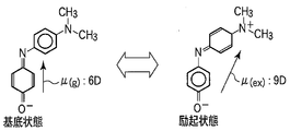
- FIG. 1 is a diagram showing an example of a dye exhibiting positive solvatochromism and dipole moments in its ground state and excited state.
- FIG. 2 is a diagram showing an example of a dye exhibiting negative solvatochromism and dipole moments in its ground state and excited state.
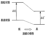
- FIG. 3 is an energy diagram of solvatochromism exhibited by the pigment shown in FIG.
- FIG. 4 is an energy diagram of solvatochromism shown by the dye shown in FIG.
- FIG. 1 shows a Phenol Blue dye as an example of a dye exhibiting positive solvatochromism.
- FIG. 2 shows a Reichardt dye as an example of a dye exhibiting negative solvatochromism. Note that the structural formulas shown in FIGS. 1 and 2 do not necessarily accurately represent the electron density in the compound.
- the solvatochromism is called a positive solvatochromism.
- the polarity of the solvent is increased, the absorption wavelength is shifted in the long wavelength direction.
- the solvatochromism is called a negative solvatochromism.
- the polarity of the solvent is increased, the absorption wavelength is shifted in the short wavelength direction.
- the value L (n 2 ) represents the electronic polarization
- the difference L ( ⁇ ) ⁇ L (n 2 ) between the value L ( ⁇ ) and the value L (n 2 ) The orientation polarization is obtained by subtracting the polarization contribution.
- the variation ⁇ E′ ⁇ E is large. That is, in this case, the color change amount of the pigment is large.
- solvatochromism can be said to be a phenomenon derived from the interaction between the dipole of the dye molecule and the dipole of the solvent existing in the vicinity of the dye molecule and the induced dipole. Therefore, if the magnitude of this interaction can be changed by an electric field, the color of the solvatochromic dye, particularly the hue, should be changed without changing the solvent.
- a material having dielectric anisotropy is positioned in the vicinity of the solvatochromic dye, and the material having dielectric anisotropy is compared with the material having dielectric anisotropy. An electric drive signal is given. This realizes a color change of the solvatochromic dye without changing the solvent.
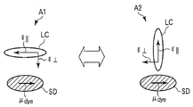
- FIG. 5 is a diagram schematically showing the relationship between the dipole moment of the dye molecule and the orientation state of the solvent molecule. Note that FIG. 5 assumes a case where a liquid crystal material is used as a material having dielectric anisotropy.
- the polarity of the solvent cannot be simply interpreted by the dielectric constant, but here, based on the McRae model, the polarity of the solvent is considered by focusing on the dielectric constant.
- the liquid crystal material is a material having a dielectric anisotropy that a dielectric constant parallel to the molecular long axis is different from a dielectric constant perpendicular to the long axis.
- the dipole moment ⁇ dye of the solvatochromic dye molecule SD is parallel to the long axis of the liquid crystal molecule LC.
- the dipole moment ⁇ dye of the solvatochromic dye molecule SD is perpendicular to the long axis of the liquid crystal molecule LC.
- the solvatochromic dye molecule SD is placed in an environment having a dielectric constant ⁇ parallel to the long axis of the liquid crystal molecule LC.
- the solvatochromic dye molecule SD is placed in an environment having a dielectric constant ⁇ perpendicular to the long axis of the liquid crystal molecule LC.
- FIG. 6 is a diagram schematically showing the interaction between the dipole of the dye molecule and the dipole of the solvent molecule and the induced dipole.
- the liquid crystal molecule LC is a nematic liquid crystal having positive dielectric anisotropy ( ⁇ > ⁇ ).
- the induced dipole moment ⁇ LC ⁇ due to the refractive index ⁇ 0 ⁇ parallel to the short axis of the liquid crystal molecule LC is perpendicular to the dipole moment ⁇ dye of the dye molecule SD.
- the dipole moment ⁇ LC of the liquid crystal molecule LC and the induced dipole moment ⁇ LC ⁇ caused by the refractive index ⁇ 0 ⁇ parallel to the long axis of the liquid crystal molecule LC are the dipole moment of the dye molecule SD. It is orthogonal to ⁇ dye . The interaction of orthogonal dipole moments is zero.
- the dipole moment ⁇ LC of the liquid crystal molecule LC and the induced dipole moment ⁇ LC ⁇ caused by the refractive index ⁇ 0 ⁇ parallel to the long axis of the liquid crystal molecule LC are It interacts with the dipole moment ⁇ dye .
- the induced dipole moment ⁇ LC ⁇ due to the refractive index ⁇ 0 ⁇ parallel to the short axis of the liquid crystal molecule LC interacts with the dipole moment ⁇ dye of the dye molecule SD.
- the interaction energy received by the dipole moment ⁇ dye of the dye molecule SD in the orientation state A1 is ⁇ dye ⁇ LC / (4 ⁇ 0 r 3 ) ⁇ 2 ⁇ dye 2 ⁇ 0 ⁇ / ((4 ⁇ 0 ) 2 r 6 ).
- the interaction energy received by the dipole moment ⁇ dye of the dye molecule SD in the orientation state A2 is ⁇ 2 ⁇ dye 2 ⁇ 0 ⁇ / ((4 ⁇ 0 ) 2 r 6 ).
- ⁇ 0 represents the dielectric constant of vacuum
- r represents the distance between the liquid crystal molecules LC and the dye molecules SD.
- the interaction between the dipole of the dye molecule SD, the dipole of the liquid crystal molecule LC, and the induced dipole is larger than that in the alignment state A2.
- the magnitude of this interaction correlates with the color of the solvatochromic dye.
- the change between the alignment state A1 and the alignment state A2 can be caused by an electric field. Therefore, when a solvatochromic dye and a liquid crystal material are combined, the color of the solvatochromic dye can be changed by an electric field. Therefore, when this technique is used, a multicolor image can be displayed without a color filter.
- the color of the solvatochromic dye correlates with the magnitude of the interaction between the dipole of the dye molecule SD, the dipole of the liquid crystal molecule LC, and the induced dipole. Therefore, when the electric field strength is changed between three or more values, three or more colors can be displayed. Therefore, when this technique is applied to a display device, a multicolor image can be displayed while adopting a relatively simple structure for the pixels.
- the magnitude of the electric field can be controlled with high accuracy. Therefore, according to the technique described above, excellent color reproducibility can be achieved.
- a liquid crystal display device using birefringence requires a polarizer.
- the technique described above utilizes absorption of a solvatochromic dye, a wide viewing angle can be easily achieved.
- this technique does not require a polarizer, so that bright display is possible.
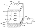
- FIG. 7 is a perspective view schematically showing that the optical element according to the first aspect of the present invention displays yellow.
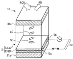
- FIG. 8 is a perspective view schematically showing how the optical element shown in FIG. 7 displays a magenta color.
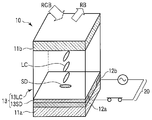
- FIG. 9 is a perspective view schematically showing that the optical element shown in FIG. 7 displays a cyan color.
- the optical element 10 shown in FIGS. 7 to 9 is a reflective optical element.
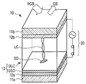
- the optical element 10 includes substrates 11a and 11b, a sealing layer (not shown), electrodes 12a and 12b, an optical variable layer 13, and a reflecting layer (not shown).
- the substrate 11a side is the back side
- the substrate 11b side is the front side.
- the substrates 11a and 11b face each other.
- the substrate 11a has light transparency and is typically colorless and / or transparent.
- the seal layer has a frame shape and is interposed between the substrates 11a and 11b.
- the substrates 11a and 11b and the sealing layer constitute a cell having a hollow structure.
- a spacer may be arranged to improve the uniformity of the distance between the substrates 11a and 11b.
- the electrodes 12a and 12b are located between the substrate 11a and the substrate 11b.
- the electrodes 12a and 12b are supported by the substrates 11a and 11b, respectively.
- the electrodes 12a and 12b are light transmissive and are typically colorless and / or transparent.
- the optically variable layer 13 includes a material having dielectric anisotropy and a solvatochromic dye. Specifically, the optical variable layer 13 includes a dye layer 13SD and a liquid crystal layer 13LC.
- the dye layer 13SD covers the electrode 12a.
- the dye layer 13SD includes a solvatochromic dye SD immobilized on the electrode 12a.
- the solvatochromic dye SD exhibits negative solvatochromism.
- the solvatochromic dye SD is oriented so that the dipole moment in the ground state or the excited state faces one direction parallel to the surface of the substrate 11a facing the substrate 11b. To do.
- this direction is referred to as “the orientation direction of the dye molecule SD”.
- An insulating layer may be interposed between the dye layer 13SD and the electrode 12a.
- the dye layer 13SD may include an insulating layer and a solvatochromic dye SD fixed thereto.
- the liquid crystal layer 13LC is interposed between the dye layer 13SD and the electrode 12b.
- the liquid crystal layer 13LC is made of a liquid crystal material that fills a sealed space surrounded by the substrates 11a and 11b and the seal layer.
- the liquid crystal material is a nematic liquid crystal having a positive dielectric anisotropy, and the major axis or the dipole moment of the liquid crystal molecules LC is substantially parallel to the alignment direction of the dye when no voltage is applied. Is oriented.
- the direction of the long axis or dipole moment of the liquid crystal molecules LC is referred to as “the alignment direction of the liquid crystal molecules LC”.
- the liquid crystal material can be aligned by, for example, providing an alignment film adjacent to the liquid crystal layer 13LC or performing an alignment process on a layer adjacent to the liquid crystal layer 13LC.
- a rubbing process or a photo-alignment technique can be used for the formation of the alignment film or the alignment process.
- the reflective layer is installed on the back side of the substrate 11a.
- the reflective layer may be disposed between the substrate 11a and the dye layer 13SD.
- a light reflective electrode such as a metal layer or an alloy layer may be used as the electrode 12a.
- the electrodes 12 a and 12 b of the optical element 10 are connected to the drive circuit 20.
- the drive circuit includes a variable voltage source.
- the variable voltage source may be an AC voltage source or a DC voltage source.
- the combination of the optical element 10 and the drive circuit 20 can be used as a display device, for example.
- the white light passes through the substrate 11b, the electrode 12b, and the liquid crystal layer 13LC in this order, and enters the dye layer 13SD.
- the dye layer 13SD absorbs part of the incident light and transmits the other part.
- the light that has passed through the dye layer 13SD passes through the substrate 11a and is reflected by the reflective layer. This reflected light passes through the substrate 11a and enters the dye layer 13SD.
- the dye layer 13SD absorbs part of the incident light and transmits the other part.
- the light that has passed through the dye layer 13SD passes through the liquid crystal layer 13LC, the electrode 12b, and the substrate 11b in this order.
- the observer perceives this transmitted light as display light. That is, the observer perceives the complementary color of the light color absorbed by the dye layer 13SD.
- the alignment direction of the liquid crystal molecules LC is parallel to the alignment direction of the dye molecules SD.
- This state corresponds to the alignment state A1 described with reference to FIGS.
- the dye layer 13SD absorbs blue light, for example. In this case, the observer perceives yellow, which is a complementary color of blue.
- the liquid crystal molecules LC are aligned substantially perpendicular to the main surface of the substrate 11a, that is, substantially perpendicular to the display surface, as shown in FIG.
- This state corresponds to the alignment state A2 described with reference to FIGS.
- the dye layer 13SD absorbs red light, for example. In this case, the observer perceives a cyan color that is a complementary color of red.
- the absorption wavelength region of the dye layer 13SD shifts in the short wavelength direction when the voltage applied between the electrodes 12a and 12b is increased. Therefore, in this case, for example, the dye layer 13SD may be designed to absorb red light when no voltage is applied to the electrodes 12a and 12b.
- the absorption wavelength region when no voltage is applied, and the shift direction and shift amount of the absorption wavelength region accompanying an increase in applied voltage can be controlled by, for example, the liquid crystal material and solvatochromic dye material used and the magnitude of the voltage.
- both the electrodes 12a and 12b are supported on the substrate 11a.
- FIG. 10 is a perspective view schematically showing that the optical element according to the second aspect of the present invention displays yellow.
- FIG. 11 is a perspective view schematically showing how the optical element shown in FIG. 10 displays a magenta color.
- FIG. 12 is a perspective view schematically showing that the optical element shown in FIG. 10 displays a cyan color.
- FIG. 13 is a diagram schematically showing solvatochromic dye molecules and liquid crystal molecules in the state shown in FIG.
- FIG. 14 is a diagram schematically showing solvatochromic dye molecules and liquid crystal molecules in the state shown in FIG.
- FIG. 15 is a diagram schematically showing solvatochromic dye molecules and liquid crystal molecules in the state shown in FIG. 13 to 15 depict the arrangement of solvatochromic dye molecules and liquid crystal molecules observed from a direction perpendicular to the display surface.
- the optical element 10 shown in FIGS. 10 to 12 has the same configuration as the optical element 10 described with reference to FIGS. 7 to 9 except that the following configuration is adopted.
- both the electrodes 12 a and 12 b are located between the substrate 11 a and the optical variable layer 13.
- the electrodes 12a and 12b each have a shape extending in one direction, and are arranged so that their length directions are parallel to each other.
- the orientation direction of the solvatochromic dye molecule SD is substantially parallel to the length direction of the electrodes 12a and 12b.
- the alignment direction of the liquid crystal molecules LC when no voltage is applied is also substantially parallel to the length direction of the electrodes 12a and 12b.
- the liquid crystal molecules LC are substantially parallel to the display surface and tilted with respect to the length direction of the electrodes 12a and 12b, as shown in FIGS. Oriented in the direction
- This state is equivalent to the state described with reference to FIG. Therefore, in this case, the observer perceives, for example, a magenta color that is a complementary color of green.
- the liquid crystal molecules LC are substantially parallel to the display surface and substantially in the length direction of the electrodes 12a and 12b, as shown in FIGS. Orient in the vertical direction.
- This state is equivalent to the state described with reference to FIG. Therefore, in this case, the observer perceives, for example, a cyan color that is a complementary color of red.
- the solvatochromic dye is not fixed but mixed with the liquid crystal material.
- FIG. 16 is a cross-sectional view schematically showing that the optical element according to the third aspect of the present invention displays a certain color.
- FIG. 17 is a cross-sectional view schematically showing how the optical element shown in FIG. 16 displays other colors.
- Reference numerals 15 and 16 denote the sealing layer and the reflective layer 16 described above, respectively.
- the optical element 10 shown in FIGS. 16 and 17 has the same configuration as the optical element 10 described with reference to FIGS. 7 to 9 except that the following configuration is adopted.
- the optical variable layer 13 has a single layer structure.
- the optically variable layer 13 is made of a mixture containing a solvatochromic dye and a liquid crystal material.
- the electrodes 12a and 12b are covered with insulating layers 17a and 17b, respectively.
- the direction of the dipole moment of the liquid crystal molecules LC is random, or the liquid crystal material is aligned with a low degree of alignment order.
- the direction of the dipole moment of the solvatochromic dye SD is random, or the solvatochromic dye SD is oriented with a low degree of orientation order.
- the direction of the dipole moment of the liquid crystal molecules LC and the direction of the dipole moment of the solvatochromic dye SD are random in the state where no voltage is applied.
- the solvatochromic dye molecule SD is placed in an average dielectric constant environment of the liquid crystal material.
- the liquid crystal molecules LC are aligned substantially perpendicular to the display surface.
- the degree of orientation order of the solvatochromic dye SD also increases.
- the color of the solvatochromic dye SD changes. That is, the display color, particularly the hue, changes.
- a solvatochromic dye SD having a negative solvatochromism such as a Reichardt dye
- the absorption spectrum of the optical variable layer 13 is Shift to short wavelength direction.
- a solvatochromic dye SD having a positive solvatochromism such as Phenol Blue dye
- the absorption spectrum of the optical variable layer 13 is increased by increasing the voltage applied between the electrodes 12a and 12b. Shifts in the long wavelength direction.
- the display color can be changed according to the magnitude of the voltage applied between the electrodes 12a and 12b.
- the optical element 10 since the solvatochromic dye and the liquid crystal material are mixed, it is not necessary to form the dye layer 13SD. Therefore, the optical element 10 is easier to manufacture than the optical element 10 described with reference to FIGS.
- the mixture containing the solvatochromic dye and the liquid crystal material may be microencapsulated. That is, the optical variable layer 13 may be configured using a microcapsule including the mixture and a transparent film containing the mixture.
- both the electrodes 12a and 12b may be supported by the substrate 11a.
- the solvatochromic dye is fixed without being oriented or with a low degree of orientation order.
- FIG. 18 is a cross-sectional view schematically showing that the optical element according to the fourth aspect of the present invention displays a certain color.
- FIG. 19 is a cross-sectional view schematically showing how the optical element shown in FIG. 18 displays other colors. 18 and 19 show only a part of the optical variable layer 13 in the optical element 10. Further, FIG. 18 illustrates a state in which no voltage is applied, and FIG. 19 illustrates a state in which a sufficiently large voltage is applied.
- the optical element 10 shown in FIGS. 18 and 19 has the same configuration as the optical element 10 described with reference to FIGS. 7 to 9 except that the following configuration is adopted.
- the optically variable layer 13 further includes a porous body 13P in addition to the solvatochromic dye SD and the liquid crystal material.
- the porous body 13P forms a layer sandwiched between the electrodes 12a and 12b.
- the solvatochromic dye SD is immobilized on the wall surfaces of the pores of the porous body 13P.
- the optical variable layer 13 displays the same color as described with reference to FIG. 7, for example.
- the liquid crystal molecules LC are aligned in approximately one direction as shown in FIG. Accordingly, the average angle formed by the dipole moment of the liquid crystal molecules LC and the dipole moment of the solvatochromic dye SD located in the vicinity thereof increases. As a result, the color of the solvatochromic dye SD changes. That is, the display color, particularly the hue, changes.
- the display color can be changed according to the magnitude of the voltage applied between the electrodes 12a and 12b.
- the area of the porous body 13P is much larger than that of the electrode 12a. Therefore, when the porous body 13P is used, more solvatochromic dye SD can be immobilized. Therefore, a higher color density can be achieved.
- both the electrodes 12a and 12b may be supported by the substrate 11a.
- the substrates 11a and 11b for example, those having sufficient strength and insulation are used.
- the substrate 11a a substrate having optical transparency, typically a transparent substrate, is used.
- substrate 11b may have a light transmittance and does not need to have it.
- a material of the substrates 11a and 11b for example, glass, plastic, ceramic and metal can be used.
- the electrode installed between the optically variable layer 13 and the observer has light transparency and is typically transparent.
- a transparent conductive material such as indium tin oxide (ITO) can be used.
- ITO indium tin oxide
- a metal such as aluminum, nickel, copper, silver, gold and platinum or an alloy thereof can be used.
- the electrodes 12a and 12b may have a single layer structure or a multilayer structure.
- the electrodes 12a and 12b are obtained, for example, by performing film formation by a vapor deposition method such as vapor deposition and sputtering, and performing patterning using, for example, photolithography as necessary.
- an adhesive can be used.
- a spacer is provided between the substrates 11a and 11b, for example, a granular spacer or a columnar spacer similar to that used in a liquid crystal display device can be used.
- the granular spacer and the columnar spacer are electrically insulating.
- the material of the granular spacer for example, polymers such as divinylbenzene and polystyrene, or inorganic oxides such as alumina and silica can be used.
- a positive or negative photosensitive resin that can use photolithography can be used.
- a photosensitive resin containing polyimide, polyamide, polyvinyl alcohol, polyacrylamide, cyclized rubber, novolac resin, polyester, polyurethane, acrylic resin, bisphenol resin, or gelatin can be used.
- the surface of at least one of the electrodes 12a and 12b may be covered with an insulating layer.
- the material for the insulating layer include polyimide, polyamide, polyvinyl alcohol, polyacrylamide, cyclized rubber, novolac resin, polyester, polyurethane, acrylic resin, bisphenol resin, gelatin, and other organic substances, or silicon oxide and silicon nitride. Inorganic materials can be used.
- the insulating layer may have a single layer structure or a multilayer structure.
- the insulating layer can be formed, for example, by a coating method such as spin coating, a Langmuir-Blodgett method in which a monomolecular film formed on the water surface is copied onto an electrode, or a vapor deposition method such as a vapor deposition method.
- the insulating layer may be subjected to an alignment treatment such as a rubbing treatment in order to control the alignment of a material having dielectric anisotropy such as a liquid crystal material.
- a material having dielectric anisotropy is a material having dielectric anisotropy in the molecule, that is, a material having anisotropy in the molecule such as orientation polarization, electronic polarization and atomic polarization. .
- the material having dielectric anisotropy may be an organic material or an inorganic material.
- a liquid crystal material As a material having dielectric anisotropy, for example, a liquid crystal material can be used.
- the liquid crystal material may be a liquid crystal compound or a composition containing a plurality of liquid crystal compounds.
- the liquid crystal material may be a composition containing one or more liquid crystal compounds and one or more other compounds.
- liquid crystal material examples include a nematic liquid crystal material, a cholesteric liquid crystal material, or a chiral nematic liquid crystal material (hereinafter referred to as a cholesteric liquid crystal material and / or a chiral nematic liquid crystal material), a nematic liquid crystal material and a cholesteric liquid crystal material, or A mixture with a chiral agent or a smectic liquid crystal material can be used.
- the material having dielectric anisotropy may be composed only of components having dielectric anisotropy, or may further include a material having no dielectric anisotropy.
- the dielectric anisotropy of the liquid crystal material preferably has a large absolute value.
- the absolute value of dielectric anisotropy which is the value obtained by subtracting the relative dielectric constant in the minor axis direction from the relative dielectric constant in the major axis direction of the liquid crystal molecules Is preferably 5 or more, more preferably 10 or more.
- solvatochromic dye a compound showing solvatochromism or a composition containing a plurality of compounds showing solvatochromism can be used.
- Examples of the compound exhibiting solvatochromism include Chem. Rev. , 94, 2319 (1994) can be used.
- the solvatochromic dye preferably has a large absorption wavelength shift amount corresponding to the change in the polarity of the solvent, such as one having an intramolecular charge transfer structure. Further, from the viewpoint of color density, the solvatochromic dye is desirably an organic material having a large absorbance. Examples of such solvatochromic dyes include Reichardt dyes.
- the solvatochromic dye may be immobilized on an organic material or an inorganic material.
- the solvatochromic dye may be incorporated in the main chain or side chain of the polymer material supported by the electrode 12a or 12b. As described above, the solvatochromic dye is preferably immobilized on the porous body.
- an alignment film When aligning a solvatochromic dye, for example, an alignment film can be used. For example, by applying a liquid containing a solvatochromic dye on the alignment film and drying the coating film, the solvatochromic dye can be oriented and fixed. Alternatively, when the solvatochromic dye is incorporated in the main chain or side chain of the polymer material, a layer containing the polymer material is formed, and the layer is subjected to stretching treatment or rubbing treatment, thereby The chromic dye can be oriented.
- the absorption axis of the solvatochromic dye is preferably substantially perpendicular to the display surface. In this case, more efficient light absorption by the solvatochromic dye material can be realized.
- the direction of the dipole moment in the ground state or excited state of the solvatochromic dye is, for example, parallel to the alignment direction in which the alignment film aligns the liquid crystal material, and between the electrodes 12a and 12b. It is perpendicular to the direction of the electric field generated when a voltage is applied to.
- the direction of the dipole moment in the ground state or excited state of the solvatochromic dye is perpendicular to the alignment direction in which the alignment film aligns the liquid crystal material, and an electric field generated when a voltage is applied between the electrodes 12a and 12b. Parallel to the direction.
- the change in the absorption wavelength accompanying the change in the applied voltage can be maximized.
- parallel means that the angle formed by the two directions is within a range of ⁇ 20 ° to + 20 °.
- “Vertical” means that the angle formed by the two directions is in the range of + 70 ° to + 110 °.
- the material of the reflective layer 16 a metal such as aluminum and silver or an alloy thereof can be used.
- the reflective layer 16 can be omitted, for example, when the electrode 12a also serves as the reflective layer or when the optical element 10 is a transmissive type.
- the color to be displayed on the optical element 10 can be controlled by the magnitude of the driving voltage.
- the drive circuit 20 outputs an alternating voltage as a drive voltage
- the color to be displayed on the optical element 10 can be controlled by at least one of the magnitude and frequency of the drive voltage.
- AC driving instead of DC driving.
- the frequency is preferably set in a range of 10 Hz to 1 KHz, more preferably 30 Hz to 240 Hz, from the viewpoint of flicker phenomenon suppression and low power consumption. Set within the range.
- the drive circuit 20 can change the absorption maximum wavelength over almost the entire visible light range, for example.
- the drive circuit 20 preferably has the maximum absorption maximum wavelength.
- the operation of the optical element 10 is controlled so that the absorption maximum wavelength changes at a maximum of 250 nm or more so as to change by 100 nm or more.
- the “visible light region” means a wavelength region of 400 nm to 800 nm.
- Example 1 the optical element 10 described with reference to FIGS. 16 and 17 was manufactured by the following method.
- Two transparent non-alkali glass substrates 11a and 11b provided with ITO electrodes 12a and 12b were prepared.
- the thickness of each glass substrate was 0.7 mm.
- an insulating layer 17a was formed on the electrode 12a by casting polyimide to a thickness of 70 nm using a spinner.
- polyimide AL-1051 manufactured by Nippon Synthetic Rubber Company was used.
- the epoxy adhesive used as the sealing layer 15 was dispensed to the peripheral part of the said main surface of the board
- the insulating layer 17b was also formed on the electrode 12b by the same method as described for the insulating layer 17a. Resin spacer balls having a diameter of 10 ⁇ m were sprayed on the insulating layer 17b.
- a mixture containing 96 parts by mass of a nematic liquid crystal material and 4 parts by mass of a solvatochromic dye was vacuum-injected into an empty cell in an isotropic phase to form the optically variable layer 13.
- a nematic liquid crystal material 4-cyano-4'-pentylbiphenyl manufactured by Aldrich-Sigma was used.
- solvatochromic dye Reichardt dye manufactured by Aldrich-Sigma was used.
- the reflective film 16 was pasted on the substrate 11a. As described above, the optical element 10 shown in FIGS. 16 and 17 was completed.
- the optical element 10 was connected to the drive circuit 20. And the alternating voltage was applied between the electrodes 12a and 12b, and the color change accompanying a voltage change was observed. In addition, the waveform of this alternating voltage was a rectangular wave, and the frequency was 30 Hz. The results are shown in FIG.
- FIG. 20 is a graph showing an example of a color change accompanying a voltage change.
- the horizontal axis indicates the wavelength
- the vertical axis indicates the absorbance (arbitrary unit).
- This optical element 10 displayed green in the state of no voltage application (0 V), and the absorption maximum wavelength at this time was 680 nm as shown in FIG.
- the optical element 10 displayed red when the applied voltage was 20 V, and the absorption maximum wavelength at this time was 580 nm as shown in FIG.
- Example 2 In this example, the optical element 10 described with reference to FIGS. 16 and 17 was manufactured by the following method. First, an empty cell was formed by the same method as described in Example 1.
- a mixture containing 96 parts by mass of a nematic liquid crystal material and 4 parts by mass of a solvatochromic dye was vacuum-injected into an empty cell in an isotropic phase to form the optically variable layer 13.
- a nematic liquid crystal material ZLI-4900-000 manufactured by Merck & Co. was used.
- solvatochromic dye Reichardt dye manufactured by Aldrich-Sigma was used.
- the reflective film 16 was pasted on the substrate 11a. As described above, the optical element 10 shown in FIGS. 16 and 17 was completed.
- the optical element 10 was connected to the drive circuit 20. And the alternating voltage was applied between the electrodes 12a and 12b, and the color change accompanying a voltage change was observed. In addition, the waveform of this alternating voltage was a rectangular wave, and the frequency was 30 Hz.
- this optical element 10 displayed a light orange color when no voltage was applied (0 V), and displayed a reddish purple color when the applied voltage was 15 V.
- FIG. 21 is a cross-sectional view schematically showing an optical element according to Example 3.
- the optical element 10 shown in FIG. 21 was manufactured by the following method.
- Two transparent non-alkali glass substrates 11a and 11b provided with ITO electrodes 12a and 12b were prepared.
- the thickness of each glass substrate was 0.7 mm.
- the electrode 12a was rubbed.
- a solution containing a solvatochromic dye was cast on the electrode 12a to a thickness of 50 nm with a spinner. Thereby, a dye layer 13SD was obtained.
- the solvatochromic dye Reichardt dye manufactured by Aldrich-Sigma was used.
- the epoxy adhesive used as the sealing layer 15 was dispensed to the peripheral part of the said main surface of the board
- polyimide was cast to a thickness of 70 nm by a spinner, and the coating film was rubbed to form an insulating layer 17b.
- the polyimide AL-1051 manufactured by Nippon Synthetic Rubber Company was used. Then, resin spacer balls having a diameter of 10 ⁇ m were dispersed on the insulating layer 17b.
- the substrates 11a and 11b were bonded so that the insulating layers 17a and 17b face each other and the rubbing directions were parallel, and the epoxy adhesive was cured. Thereby, an empty cell was obtained.
- nematic liquid crystal material JC-1041 manufactured by Chisso Corporation was used.
- the reflective film 16 was pasted on the substrate 11a. As described above, the optical element 10 shown in FIG. 21 was completed.
- the optical element 10 was connected to the drive circuit 20. And the alternating voltage of 30V was applied between the electrodes 12a and 12b, and the color change accompanying a voltage change was observed. In addition, the waveform of this alternating voltage was a rectangular wave, and the frequency was 30 Hz. The results are shown in FIG.
- FIG. 22 is a graph showing another example of color change accompanying voltage change.
- the horizontal axis indicates the wavelength
- the vertical axis indicates the absorbance (arbitrary unit).
- a curve C OFF shows an absorption spectrum in a state where no voltage is applied. Curves C ON (0), C ON (30), and C ON (90) are respectively applied immediately after the voltage is applied, after 30 seconds from the start of the voltage application, and after the voltage application is started. An absorption spectrum after 90 seconds has been shown.
- the optical element 10 shown in FIG. 21 was manufactured by the following method. Two transparent non-alkali glass substrates 11a and 11b provided with ITO electrodes 12a and 12b, respectively, were prepared. The thickness of each glass substrate was 0.7 mm.
- the electrode 12a was rubbed.
- a liquid containing a polymer having a solvatochromic dye in the side chain was cast on the electrode 12a with a spinner to a thickness of 30 nm. Further, the coating layer was rubbed to obtain a dye layer 13SD.
- this polymer a compound represented by the following chemical formula was used. Then, the epoxy adhesive used as the sealing layer 15 was dispensed to the peripheral part of the said main surface of the board
- polyimide was cast to a thickness of 70 nm by a spinner, and the coating film was rubbed to form an insulating layer 17b.
- the polyimide AL-1051 manufactured by Nippon Synthetic Rubber Company was used. Then, resin spacer balls having a diameter of 10 ⁇ m were dispersed on the insulating layer 17b.
- the substrates 11a and 11b were bonded so that the insulating layers 17a and 17b face each other and the rubbing directions were parallel, and the epoxy adhesive was cured. Thereby, an empty cell was obtained.
- nematic liquid crystal material manufactured by Merck was vacuum-injected into an empty cell in a liquid crystal phase to form a liquid crystal layer 13LC.
- a nematic liquid crystal material having a dielectric anisotropy ⁇ of 20 and a refractive index anisotropy ⁇ n of 0.15 was used.
- the reflective film 16 was pasted on the substrate 11a. As described above, the optical element 10 shown in FIG. 21 was completed.
- the optical element 10 was connected to the drive circuit 20. And the alternating voltage was applied between the electrodes 12a and 12b, and the color change accompanying a voltage change was observed. In addition, the waveform of this alternating voltage was a rectangular wave, and the frequency was 30 Hz.
- the optical element 10 displayed red when no voltage was applied (0 V), and displayed green when the applied voltage was 15 V.
- Example 5 the optical element described with reference to FIGS. 18 and 19 was manufactured by the following method.
- porous glass beads 13P having a thickness of 3 ⁇ m and a pore diameter of 1 ⁇ m were prepared by heat treatment of borosilicate soda glass and subsequent acid treatment.
- the porous glass beads were impregnated with an ethanol solution of Reichardt dye to immobilize the Reichardt dye on the walls of the pores.
- the particles thus obtained were encapsulated in a cell composed of two transparent glass substrates provided with ITO electrodes on the surface thereof and a sealing layer.
- a non-alkali glass substrate having a thickness of 0.7 mm was used as the glass substrate.
- nematic liquid crystal material manufactured by Merck was vacuum-injected into the cell in an isotropic phase.
- a nematic liquid crystal material having a dielectric anisotropy ⁇ of 15 and a refractive index anisotropy ⁇ n of 0.18 was used.
- the reflective film 16 was pasted on one substrate. As described above, the optical element described with reference to FIGS. 18 and 19 was completed.
- the optical element 10 was connected to the drive circuit 20. And the alternating voltage was applied between the electrodes 12a and 12b, and the color change accompanying a voltage change was observed. In addition, the waveform of this alternating voltage was a rectangular wave, and the frequency was 30 Hz.
- this optical element 10 displayed reddish purple when no voltage was applied (0 V), and displayed yellowish green when the applied voltage was 50 V.
Landscapes
- Chemical & Material Sciences (AREA)
- Physics & Mathematics (AREA)
- Organic Chemistry (AREA)
- Nonlinear Science (AREA)
- Mathematical Physics (AREA)
- Crystallography & Structural Chemistry (AREA)
- General Physics & Mathematics (AREA)
- Optics & Photonics (AREA)
- Liquid Crystal (AREA)
- Electrochromic Elements, Electrophoresis, Or Variable Reflection Or Absorption Elements (AREA)
Abstract
多色画像を優れた色再現性で表示可能とする。光学素子(10)は、誘電率異方性を有する材料(LC)とソルバトクロミック色素(SD)とを含んだ光学的可変層(13)と、光学的可変層(13)に電圧を印加する電極(12a,12b)とを含んでいる。
Description
本発明は、光学技術に関する。
電子ペーパは、表示すべき画像の変更が可能であり、紙に匹敵する携帯性を有している表示装置である。電子ペーパは、情報伝達に使用する紙の一部を置換し得る。それ故、電子ペーパは、森林資源の保護に寄与し得る。
このような表示装置において多色画像を表示すべくカラーフィルタを使用した場合、高い解像度と紙に匹敵する厚さとを達成することは難しい。また、表示すべき画像の変更は、電気的な手法によって行うことが有利である。即ち、カラーフィルタなしで多色画像を表示可能であることが望ましい。
特開2007-11260号公報、特開2007-240668号公報及び特開2007-279163号公報には、金属イオンを含んだ電解液を使用する表示技術が記載されている。この表示技術では、電解液に通電することによって、電解液から金属を析出させる。表示色は、例えば金属微粒子の粒径に応じて変化する。従って、この表示技術によると、カラーフィルタなしで多色画像を表示することが可能である。
しかしながら、金属微粒子の粒径を高い精度で制御することは困難である。それ故、先の表示技術によると、色再現性が不十分になり易い。
本発明の目的は、多色画像を優れた色再現性で表示可能とすることにある。
本発明の目的は、多色画像を優れた色再現性で表示可能とすることにある。
本発明の第1側面によると、誘電率異方性を有する材料とソルバトクロミック色素とを含んだ光学的可変層と、前記光学的可変層に電圧を印加する第1及び第2電極とを具備した光学素子が提供される。
本発明の第2側面によると、第1側面に係る光学素子と、前記第1及び第2電極間に駆動電圧を印加する駆動回路とを含んだ表示装置が提供される。
以下、本発明の態様について、図面を参照しながら詳細に説明する。なお、同様又は類似した機能を発揮する構成要素には全ての図面を通じて同一の参照符号を付し、重複する説明は省略する。
まず、ソルバトクロミズムについて説明する。
ソルバトクロミズムは、溶媒の種類に応じて色素溶液の色が変化する現象であり、次のように解釈されている。
ソルバトクロミズムは、溶媒の種類に応じて色素溶液の色が変化する現象であり、次のように解釈されている。
大きな電気双極子モーメント(以下、「双極子モーメント」は、「電気双極子モーメント」を意味することとする)を有しており、基底状態と励起状態とで双極子モーメントの大きさが著しく異なる色素分子は、溶媒の極性が高いほど基底状態又は励起状態の一方がより安定化される。その結果、基底状態から励起状態への電子遷移エネルギーが変化し、吸収波長のシフトを引き起こす。この現象はソルバトクロミズムと呼ばれており、このような色素はソルバトクロミック色素と呼ばれている。
ソルバトクロミズムについて、数式及び図面を参照しながら、更に詳しく説明する。

ソルバトクロミズムについて、数式及び図面を参照しながら、更に詳しく説明する。
上記数式(1)において、ΔE及びΔE’は、それぞれ、溶媒の極性が低い場合及び高い場合におけるソルバトクロミック色素の基底状態から励起状態への電子遷移エネルギーを表している。μ(g)及びμ(ex)は、それぞれ、基底状態及び励起状態における色素分子の双極子モーメントを表している。ε及びnは、それぞれ、溶媒の誘電率及び屈折率を表している。なお、等式(1)におけるL(ε)及びL(n2)の各々は、上記等式(2)から算出される値である。
数式(1)は、溶媒の極性が高い場合における電子遷移エネルギーΔE’と溶媒の極性が低い場合の電子遷移エネルギーΔEとの差、即ち電子遷移エネルギーの変化量ΔE’―ΔEが、双極子モーメントμ(g)及びμ(ex)と誘電率εと屈折率nとの関数であることを示すものであり、McRaeモデルと呼ばれている。ここでは、簡単のため、励起状態の双極子モーメントと基底状態の双極子モーメントとが成す角度は0°(又は180°)としている。なお、溶媒の極性の概念には、水素結合性や電子供与性も含まれるが、McRaeモデルではこれらは考慮されていない。
数式(1)から、色素の基底状態と励起状態とで双極子モーメントの大きさが著しく異なっていることが分かる。即ち、双極子モーメントμ(ex)の大きさと双極子モーメントμ(g)の大きさとの差μ(ex)-μ(g)が大きい場合には変化量ΔE’―ΔEが大きいことと、双極子モーメントμ(ex)及びμ(g)の各々が大きい場合には変化量ΔE’―ΔEが大きいことが分かる。換言すれば、色素の双極子モーメントと吸収波長のシフト量、即ち色の変化量との関係が分かる。また、変化量ΔE’―ΔEの極性、即ち吸収波長の変化の方向は、差μ(ex)-μ(g)の符号に依存していることが分かる。
図1は、正のソルバトクロミズムを示す色素の一例と、その基底状態及び励起状態における双極子モーメントとを示す図である。図2は、負のソルバトクロミズムを示す色素の一例と、その基底状態及び励起状態における双極子モーメントとを示す図である。図3は、図1に示す色素が示すソルバトクロミズムのエネルギー図である。図4は、図2に示す色素が示すソルバトクロミズムのエネルギー図である。図1には、正のソルバトクロミズムを示す色素の一例として、Phenol Blue色素を示している。図2には、負のソルバトクロミズムを示す色素の一例として、Reichardt色素を示している。なお、図1及び図2に示す構造式は、必ずしも化合物内における電子密度を正確に表現しているものではない。
図1に示すように差μ(ex)-μ(g)が正の値である場合、ソルバトクロミズムは、正のソルバトクロミズムと呼ばれる。この場合、図3に示すように、溶媒の極性を高めると、吸収波長は長波長方向にシフトする。
図2に示すように差μ(ex)-μ(g)が正の値である場合、ソルバトクロミズムは、負のソルバトクロミズムと呼ばれる。この場合、図4に示すように、溶媒の極性を高めると、吸収波長は短波長方向にシフトする。
溶媒がソルバトクロミズムに及ぼす影響について、更に詳しく説明する。
等式(1)において、値L(n2)は電子分極を表し、値L(ε)と値L(n2)との差L(ε)-L(n2)は、誘電率から電子分極の寄与を差し引いたものである配向分極を表している。等式(1)から分かるように、溶媒の配向分極及び電子分極が大きい場合、変化量ΔE’―ΔEが大きい。即ち、この場合、色素の色変化量が大きい。
等式(1)において、値L(n2)は電子分極を表し、値L(ε)と値L(n2)との差L(ε)-L(n2)は、誘電率から電子分極の寄与を差し引いたものである配向分極を表している。等式(1)から分かるように、溶媒の配向分極及び電子分極が大きい場合、変化量ΔE’―ΔEが大きい。即ち、この場合、色素の色変化量が大きい。
溶媒の配向分極は、溶媒の双極子に起因するものである。他方、溶媒の電子分極は、溶媒の誘起双極子に起因するものである。それ故、ソルバトクロミズムは、色素分子の双極子と色素分子の近傍に存在している溶媒の双極子及び誘起双極子との相互作用に由来した現象であると言える。従って、この相互作用の大きさを電場によって変化させることができれば、溶媒を変えることなしに、ソルバトクロミック色素の色、特には色相を変化させることができる筈である。
そこで、後で詳しく説明する本発明の各態様では、誘電率異方性を有している材料をソルバトクロミック色素の近傍に位置させ、誘電率異方性を有している材料に対して電気駆動信号を与える。これにより、溶媒を変えることなしに、ソルバトクロミック色素の色変化を実現する。
この色変化について、図5及び図6を参照しながら説明する。
図5は、色素分子の双極子モーメントと溶媒分子の配向状態との関係を概略的に示す図である。なお、図5は、誘電率異方性を有している材料として液晶材料を使用した場合を想定している。
図5は、色素分子の双極子モーメントと溶媒分子の配向状態との関係を概略的に示す図である。なお、図5は、誘電率異方性を有している材料として液晶材料を使用した場合を想定している。
前述の通り、溶媒の極性は、単純に誘電率で解釈できるものではないが、ここでは、McRaeモデルに基づき、誘電率に着目して溶媒の極性を考える。
液晶材料は、分子長軸に平行な誘電率と長軸に垂直な誘電率とが異なるという誘電率異方性を有している材料である。
図5に示す配向状態A1では、ソルバトクロミック色素分子SDの双極子モーメントμdyeは、液晶分子LCの長軸に対して平行である。他方、図5に示す配向状態A2では、ソルバトクロミック色素分子SDの双極子モーメントμdyeは、液晶分子LCの長軸に対して垂直である。
従って、配向状態A1では、ソルバトクロミック色素分子SDは、液晶分子LCの長軸に平行な誘電率ε∥の環境下に置かれていると考えられる。他方、配向状態A2では、ソルバトクロミック色素分子SDは、液晶分子LCの長軸に垂直な誘電率ε⊥の環境下に置かれていると考えられる。
図6は、色素分子の双極子と溶媒分子の双極子及び誘起双極子との相互作用を概略的に示す図である。ここでは、液晶分子LCは、正の誘電異方性(ε∥>ε⊥)を有しているネマチック液晶であるとする。
配向状態A1では、液晶分子LCの短軸に平行な屈折率α0⊥に起因する誘起双極子モーメントμLC⊥は、色素分子SDの双極子モーメントμdyeに対して垂直である。他方、配向状態A2では、液晶分子LCの双極子モーメントμLC及び液晶分子LCの長軸に平行な屈折率α0∥に起因する誘起双極子モーメントμLC∥は、色素分子SDの双極子モーメントμdyeと直交している。直交している双極子モーメントの相互作用はゼロである。
それ故、配向状態A1では、液晶分子LCの双極子モーメントμLCと、液晶分子LCの長軸に平行な屈折率α0∥に起因する誘起双極子モーメントμLC∥とが、色素分子SDの双極子モーメントμdyeと相互作用する。他方、配向状態A2では、液晶分子LCの短軸に平行な屈折率α0⊥に起因する誘起双極子モーメントμLC⊥が、色素分子SDの双極子モーメントμdyeと相互作用する。
従って、配向状態A1において色素分子SDの双極子モーメントμdyeが受ける相互作用エネルギーは、-μdyeμLC/(4πε0r3)-2μdye
2α0∥/((4πε0)2r6)である。そして、配向状態A2において色素分子SDの双極子モーメントμdyeが受ける相互作用エネルギーは、-2μdye
2α0⊥/((4πε0)2r6)である。なお、ここで、ε0は真空の誘電率を表し、rは液晶分子LCと色素分子SDの距離を表している。
このように、配向状態A1は、配向状態A2と比較して、色素分子SDの双極子と液晶分子LCの双極子及び誘起双極子との相互作用が大きい。上記の通り、この相互作用の大きさは、ソルバトクロミック色素の色と相関している。そして、配向状態A1と配向状態A2との間の変化は、電場によって生じさせることができる。従って、ソルバトクロミック色素と液晶材料とを組み合わせると、ソルバトクロミック色素の色を電場によって変化させることができる。それ故、この技術を利用すると、カラーフィルタなしで多色画像を表示することができる。
また、上記の通り、ソルバトクロミック色素の色は、色素分子SDの双極子と液晶分子LCの双極子及び誘起双極子との相互作用の大きさと相関している。従って、電場の強さを3つ以上の値の間で変化させると、3つ以上の色を表示することができる。それ故、この技術を表示装置に適用した場合、画素に比較的単純な構造を採用しながらも、多色画像を表示することができる。
例えば、減法混色を利用したゲスト-ホストモードの液晶表示装置では、3原色に対応した3つの液晶層を積層する必要がある。これに対し、上述した技術によると、ソルバトクロミック色素と液晶材料とを含んだ単一の層に、例えば、3原色、それらの中間色及び白色を表示させることができる。それ故、高精細化した場合であっても、視差に起因した表示品位の劣化を生じ難い。
更に、電場の大きさは、高い精度で制御できる。従って、上述した技術によると、優れた色再現性を達成できる。
また、複屈折を利用した液晶表示装置では、広い視野角を達成することが難しい。加えて、複屈折を利用した液晶表示装置では、偏光子が必要である。これに対し、上述した技術では、ソルバトクロミック色素の吸収を利用しているため、広い視野角を容易に達成することができる。しかも、この技術では、偏光子は不要であるため、明るい表示が可能である。
次に、上述した技術を適用した光学素子について説明する。
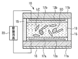
図7は、本発明の第1態様に係る光学素子が黄色を表示している様子を概略的に示す斜視図である。図8は、図7に示す光学素子がマゼンタ色を表示している様子を概略的に示す斜視図である。図9は、図7に示す光学素子がシアン色を表示している様子を概略的に示す斜視図である。
図7は、本発明の第1態様に係る光学素子が黄色を表示している様子を概略的に示す斜視図である。図8は、図7に示す光学素子がマゼンタ色を表示している様子を概略的に示す斜視図である。図9は、図7に示す光学素子がシアン色を表示している様子を概略的に示す斜視図である。
図7乃至図9に示す光学素子10は、反射型の光学素子である。この光学素子10は、基板11a及び11bと、図示しないシール層と、電極12a及び12bと、光学的可変層13と、図示しない反射層とを含んでいる。この光学素子10は、基板11a側が背面側であり、基板11b側が前面側である。
基板11a及び11bは、互いに向き合っている。基板11aは、光透過性を有しており、典型的には無色及び/又は透明である。
シール層は、枠形状を有しており、基板11a及び11b間に介在している。基板11a及び11bとシール層とは、中空構造を有しているセルを構成している。なお、このセル内には、基板11a及び11b間の距離の均一性を向上させるべく、スペーサを配置してもよい。
電極12a及び12bは、基板11aと基板11bとの間に位置している。電極12a及び12bは、それぞれ、基板11a及び11bに支持されている。電極12a及び12bは、光透過性を有しており、典型的には無色及び/又は透明である。
光学的可変層13は、誘電率異方性を有する材料とソルバトクロミック色素とを含んでいる。具体的には、光学的可変層13は、色素層13SDと液晶層13LCとを含んでいる。
色素層13SDは、電極12aを被覆している。色素層13SDは、電極12a上に固定化されたソルバトクロミック色素SDを含んでいる。ここでは、一例として、ソルバトクロミック色素SDは、負のソルバトクロミズムを示すとする。また、ここでは、一例として、ソルバトクロミック色素SDは、基底状態又は励起状態における双極子モーメントが基板11aの基板11bとの対向面に対して平行な1方向を向くように配向しているとする。以下、この方向を、「色素分子SDの配向方向」と呼ぶ。なお、色素層13SDと電極12aとの間には、絶縁層が介在していてもよい。或いは、色素層13SDは、絶縁層とこれに固定化されたソルバトクロミック色素SDとを含んでいてもよい。
液晶層13LCは、色素層13SDと電極12bとの間に介在している。液晶層13LCは、基板11a及び11bとシール層とによって囲まれた密閉空間を満たした液晶材料からなる。ここでは、一例として、液晶材料は、誘電率異方性が正のネマチック液晶であり、電圧無印加状態において、液晶分子LCの長軸又は双極子モーメントが色素の配向方向と略平行となるように配向しているとする。以下、液晶分子LCの長軸又は双極子モーメントの方向を、「液晶分子LCの配向方向」と呼ぶ。
なお、液晶材料は、例えば、液晶層13LCに隣接して配向膜を設けるか、又は、液晶層13LCに隣接した層に配向処理を施すことにより配向させることができる。配向膜の形成又は配向処理には、例えば、ラビング処理又は光配向技術を利用することができる。
反射層は、基板11aの背面側に設置されている。反射層は、基板11aと色素層13SDとの間に設置してもよい。或いは、反射層を設ける代わりに、電極12aとして、金属層又は合金層などの光反射性の電極を使用してもよい。
この光学素子10の電極12a及び12bは、駆動回路20に接続されている。駆動回路は、可変電圧源を含んでいる。可変電圧源は、交流電圧源であってもよく、直流電圧源であってもよい。
なお、光学素子10と駆動回路20との組み合わせは、例えば、表示装置として利用することができる。
この光学素子10を前方から白色光で照明すると、この白色光は、基板11b、電極12b及び液晶層13LCをこの順に透過し、色素層13SDに入射する。色素層13SDは、この入射光の一部を吸収し、他の一部を透過させる。色素層13SDを透過した光は、基板11aを透過し、反射層によって反射される。この反射光は、基板11aを透過し、色素層13SDに入射する。色素層13SDは、この入射光の一部を吸収し、他の一部を透過させる。色素層13SDを透過した光は、液晶層13LC、電極12b及び基板11bをこの順に透過する。観察者は、この透過光を表示光として知覚する。即ち、観察者は、色素層13SDが吸収した光の色の補色を知覚する。
図7に示すように、電極12a及び12bに電圧を印加していない場合、液晶分子LCの配向方向は、色素分子SDの配向方向に対して平行である。この状態は、図5及び図6を参照しながら説明した配向状態A1に相当している。この状態では、色素層13SDは、例えば青色の光を吸収する。この場合、観察者は、青色の補色である黄色を知覚する。
電極12a及び12bに絶対値が比較的小さな電圧(以下、「電圧」は「電圧の絶対値」を意味していることとする)を印加すると、液晶分子LCは、図8に示すように、基板11aに対して傾く。その結果、色素層13SDの吸収波長域は、長波長方向にシフトする。この状態では、色素層13SDは、例えば緑色の光を吸収する。この場合、観察者は、緑色の補色であるマゼンタ色を知覚する。
電極12a及び12bに印加する電圧を更に高くすると、液晶分子LCは、図9に示すように、基板11aの主面に対して略垂直に、即ち、表示面に対して略垂直に配向する。この状態は、図5及び図6を参照しながら説明した配向状態A2に相当している。この状態では、色素層13SDは、例えば赤色の光を吸収する。この場合、観察者は、赤色の補色であるシアン色を知覚する。
なお、正のソルバトクロミズムを示すソルバトクロミック色素SDを使用した場合、電極12a及び12b間に印加する電圧を高めると、色素層13SDの吸収波長域は短波長方向にシフトする。従って、この場合、例えば、電極12a及び12bに電圧を印加していないときに、色素層13SDが赤色の光を吸収するように設計してもよい。電圧無印加時における吸収波長域、並びに、印加電圧の上昇に伴う吸収波長域のシフト方向及びシフト量は、例えば、使用する液晶材料及びソルバトクロミック色素材料並びに電圧の大きさによって制御できる。
次に、本発明の第2態様を説明する。第2態様では、電極12a及び12bをそれぞれ基板11a及び11bに支持させる代わりに、電極12a及び12bの双方を基板11aに支持させる。
図10は、本発明の第2態様に係る光学素子が黄色を表示している様子を概略的に示す斜視図である。図11は、図10に示す光学素子がマゼンタ色を表示している様子を概略的に示す斜視図である。図12は、図10に示す光学素子がシアン色を表示している様子を概略的に示す斜視図である。
図13は、図11に示す状態におけるソルバトクロミック色素分子と液晶分子とを概略的に示す図である。図14は、図12に示す状態におけるソルバトクロミック色素分子と液晶分子とを概略的に示す図である。図15は、図13に示す状態におけるソルバトクロミック色素分子と液晶分子とを概略的に示す図である。なお、図13乃至図15は、表示面に垂直な方向から観察したソルバトクロミック色素分子及び液晶分子の配置を描いている。
図10乃至図12に示す光学素子10は、以下の構成を採用したこと以外は、図7乃至図9を参照しながら説明した光学素子10と同様の構成を有している。
即ち、この光学素子10では、電極12a及び12bの双方が基板11aと光学的可変層13との間に位置している。電極12a及び12bは、各々が一方向に延びた形状を有しており、それらの長さ方向が平行になるように配置されている。ソルバトクロミック色素分子SDの配向方向は、電極12a及び12bの長さ方向に対して略平行である。そして、液晶分子LCの電圧無印加状態における配向方向も、電極12a及び12bの長さ方向に対して略平行である。
電極12a及び12bに電圧を印加していない場合、液晶分子LCの配向方向は、図10及び図13に示すように、色素分子SDの配向方向に対して平行である。この状態は、図7を参照しながら説明した状態と同様である。従って、この場合、観察者は、例えば、青色の補色である黄色を知覚する。
電極12a及び12bに比較的低い電圧を印加すると、液晶分子LCは、図11及び図14に示すように、表示面に対して略平行であり且つ電極12a及び12bの長さ方向に対して傾いた方向に配向する。この状態は、図8を参照しながら説明した状態と等価である。従って、この場合、観察者は、例えば、緑色の補色であるマゼンタ色を知覚する。
電極12a及び12bに印加する電圧を更に高くすると、液晶分子LCは、図12及び図15に示すように、表示面に対して略平行であり且つ電極12a及び12bの長さ方向に対して略垂直な方向に配向する。この状態は、図9を参照しながら説明した状態と等価である。従って、この場合、観察者は、例えば、赤色の補色であるシアン色を知覚する。
次に、本発明の第3態様を説明する。第3態様では、ソルバトクロミック色素を固定化せずに、液晶材料と混合する。
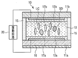
図16は、本発明の第3態様に係る光学素子が或る色を表示している様子を概略的に示す断面図である。図17は、図16に示す光学素子が他の色を表示している様子を概略的に示す断面図である。なお、参照符号15及び16は、それぞれ、上述したシール層及び反射層16を示している。
図16及び図17に示す光学素子10は、以下の構成を採用したこと以外は、図7乃至図9を参照しながら説明した光学素子10と同様の構成を有している。
即ち、この光学素子10では、光学的可変層13は、単層構造を有している。光学的可変層13は、ソルバトクロミック色素と液晶材料とを含んだ混合物からなる。そして、電極12a及び12bは、それぞれ、絶縁層17a及び17bによって被覆されている。
図16に示すように、電圧無印加状態においては、液晶分子LCの双極子モーメントの向きはランダムであるか、又は、液晶材料は低い配向秩序度で配向している。同様に、ソルバトクロミック色素SDの双極子モーメントの向きはランダムであるか、又は、ソルバトクロミック色素SDは低い配向秩序度で配向している。ここでは、一例として、電圧無印加状態において、液晶分子LCの双極子モーメントの向き及びソルバトクロミック色素SDの双極子モーメントの向きはランダムであるとする。この場合、ソルバトクロミック色素分子SDは、液晶材料の平均的な誘電率環境下に置かれている。
電極12a及び12b間に十分に高い電圧を印加すると、液晶分子LCは、表示面に対して略垂直に配向する。これに伴い、ソルバトクロミック色素SDの配向秩序度も高くなる。その結果、ソルバトクロミック色素SDの色が変化する。即ち、表示色、特には色相が変化する。
例えば、ソルバトクロミック色素SDとして、Reichardt色素などの負のソルバトクロミズムを示すものを用いた場合には、電極12a及び12b間に印加する電圧を高くすると、光学的可変層13の吸収スペクトルは短波長方向へとシフトする。他方、ソルバトクロミック色素SDとして、Phenol Blue色素などの正のソルバトクロミズムを示すものを用いた場合には、電極12a及び12b間に印加する電圧を高くすると、光学的可変層13の吸収スペクトルは長波長方向へとシフトする。
このように、ソルバトクロミック色素と液晶材料とを混合した場合であっても、電極12a及び12b間に印加する電圧の大きさに応じた表示色の変化を生じさせることができる。
また、この光学素子10では、ソルバトクロミック色素と液晶材料とを混合しているので、色素層13SDを形成する必要がない。従って、この光学素子10は、図7乃至図9を参照しながら説明した光学素子10と比較して製造が容易である。
ソルバトクロミック色素と液晶材料とを含んだ混合は、マイクロカプセル化してもよい。即ち、この混合物とこれを収容した透明膜とを含んだマイクロカプセルを用いて、光学的可変層13を構成してもよい。
ソルバトクロミック色素の一部のみを液晶材料と混合し、ソルバトクロミック色素の残りを固定化してもよい。また、電極12a及び12bの双方を基板11aに支持させてもよい。
次に、本発明の第4態様を説明する。第4態様では、ソルバトクロミック色素を配向させることなしに又は低い配向秩序度で配向させて固定化する。
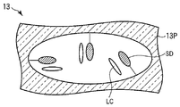
図18は、本発明の第4態様に係る光学素子が或る色を表示している様子を概略的に示す断面図である。図19は、図18に示す光学素子が他の色を表示している様子を概略的に示す断面図である。なお、図18及び図19には、光学素子10のうち光学的可変層13の一部のみを描いている。また、図18には電圧無印加状態を描いており、図19には、十分な大きさの電圧を印加した状態を描いている。
図18及び図19に示す光学素子10は、以下の構成を採用したこと以外は、図7乃至図9を参照しながら説明した光学素子10と同様の構成を有している。
即ち、この光学素子10では、光学的可変層13は、ソルバトクロミック色素SD及び液晶材料に加えて、多孔質体13Pを更に含んでいる。多孔質体13Pは、電極12a及び12b間に挟まれた層を形成している。ソルバトクロミック色素SDは、多孔質体13Pの細孔の壁面上に固定化されている。
電圧無印加状態では、図18に示すように、液晶分子LCの双極子モーメントは、その近傍に位置したソルバトクロミック色素SDの双極子モーメントに対して略平行である。従って、光学的可変層13は、例えば、図7を参照しながら説明したのと同様の色を表示する。
電極12a及び12b間に十分に高い電圧を印加すると、図19に示すように、液晶分子LCは、略一方向に配向する。これに伴い、液晶分子LCの双極子モーメントとその近傍に位置したソルバトクロミック色素SDの双極子モーメントとが成す平均角度が大きくなる。その結果、ソルバトクロミック色素SDの色が変化する。即ち、表示色、特には色相が変化する。
このように、ソルバトクロミック色素を多孔質体上に固定化した場合であっても、電極12a及び12b間に印加する電圧の大きさに応じた表示色の変化を生じさせることができる。
また、多孔質体13Pは、電極12aと比較して面積が遥かに大きい。従って、多孔質体13Pを使用した場合、より多くのソルバトクロミック色素SDを固定化することができる。それ故、より高い色濃度を達成できる。
なお、ソルバトクロミック色素の一部のみ固定化し、ソルバトクロミック色素の残りを液晶材料と混合してもよい。また、電極12a及び12bの双方を基板11aに支持させてもよい。
次に、上述した光学素子10の材料等について説明する。
基板11a及び11bとしては、例えば、十分な強度と絶縁性とを有しているものを使用する。基板11aとしては、光透過性を有している基板、典型的には透明基板を使用する。基板11bは、光透過性を有していてもよく、有していなくてもよい。基板11a及び11bの材料としては、例えば、ガラス、プラスチック、セラミック及び金属を使用することができる。
基板11a及び11bとしては、例えば、十分な強度と絶縁性とを有しているものを使用する。基板11aとしては、光透過性を有している基板、典型的には透明基板を使用する。基板11bは、光透過性を有していてもよく、有していなくてもよい。基板11a及び11bの材料としては、例えば、ガラス、プラスチック、セラミック及び金属を使用することができる。
電極12a及び12bのうち、光学的可変層13と観察者との間に設置するものは、光透過性を有しており、典型的には透明である。光透過性を有している電極の材料としては、例えば、インジウム錫酸化物(ITO)などの透明導電性材料を使用することができる。不透明又は半透明な電極の材料としては、例えば、アルミニウム、ニッケル、銅、銀、金及び白金など金属又はそれらの合金を使用することができる。電極12a及び12bは、単層構造を有していてもよく、多層構造を有していてもよい。電極12a及び12bは、例えば、蒸着及びスパッタリングなどの気相堆積法による成膜を行い、必要に応じて例えばフォトリソグラフィを利用したパターニングを行うことにより得られる。
シール層15の材料としては、例えば接着剤を使用することができる。
基板11a及び11b間にスペーサを設置する場合、スペーサとしては、例えば、液晶表示装置で使用されているのと同様の粒状スペーサ又は柱状スペーサを使用することができる。粒状スペーサ及び柱状スペーサは、電気的に絶縁性である。粒状スペーサの材料としては、例えば、ジビニルベンゼン及びポリスチレンなどの高分子、又は、アルミナ及びシリカなどの無機酸化物を使用することができる。柱状スペーサの材料としては、例えば、フォトリソグラフィを利用可能なポジ型又はネガ型の感光性樹脂を使用することができる。例えば、ポリイミド、ポリアミド、ポリビニルアルコール、ポリアクリルアミド、環化ゴム、ノボラック樹脂、ポリエステル、ポリウレタン、アクリル樹脂、ビスフェノール樹脂又はゼラチンを含んだ感光性樹脂を使用することができる。
基板11a及び11b間にスペーサを設置する場合、スペーサとしては、例えば、液晶表示装置で使用されているのと同様の粒状スペーサ又は柱状スペーサを使用することができる。粒状スペーサ及び柱状スペーサは、電気的に絶縁性である。粒状スペーサの材料としては、例えば、ジビニルベンゼン及びポリスチレンなどの高分子、又は、アルミナ及びシリカなどの無機酸化物を使用することができる。柱状スペーサの材料としては、例えば、フォトリソグラフィを利用可能なポジ型又はネガ型の感光性樹脂を使用することができる。例えば、ポリイミド、ポリアミド、ポリビニルアルコール、ポリアクリルアミド、環化ゴム、ノボラック樹脂、ポリエステル、ポリウレタン、アクリル樹脂、ビスフェノール樹脂又はゼラチンを含んだ感光性樹脂を使用することができる。
電極12a及び12bの少なくとも一方の表面を、絶縁層で被覆してもよい。絶縁層の材料としては、例えば、ポリイミド、ポリアミド、ポリビニルアルコール、ポリアクリルアミド、環化ゴム、ノボラック樹脂、ポリエステル、ポリウレタン、アクリル樹脂、ビスフェノール樹脂及びゼラチンなどの有機物、又は、酸化シリコン及び窒化シリコンなどの無機物を使用することができる。絶縁層は、単層構造を有していてもよく、多層構造を有していてもよい。絶縁層は、例えば、スピンコートなどの塗布法、水面上に形成された単分子膜を電極上に写し取るラングミュア・ブロジェット法、又は蒸着法などの気相堆積法により形成することができる。絶縁層には、液晶材料などの誘電率異方性を有する材料の配向を制御するために、ラビング処理などの配向処理を施してもよい。
誘電率異方性を有している材料は、分子内に誘電率異方性を有するもの、即ち、配向分極、電子分極及び原子分極などの分極が分子内で異方性を有するものである。誘電率異方性を有している材料は、有機材料であってもよく、無機材料であってもよい。
誘電率異方性を有している材料としては、例えば、液晶材料を使用することができる。液晶材料は、液晶化合物であってもよく、複数の液晶化合物を含んだ組成物であってもよい。或いは、液晶材料は、1つ以上の液晶化合物と他の1つ以上の化合物とを含んだ組成物であってもよい。液晶材料としては、例えば、ネマチック液晶材料、コレステリック液晶材料若しくはカイラルネマチック液晶材料(以下、コレステリック液晶材料及び/又はカイラルネマチック液晶材料を「コレステリック液晶材料」と呼ぶ)、ネマチック液晶材料とコレステリック液晶材料若しくはカイラル剤との混合物、又はスメクチック液晶材料を使用することができる。誘電率異方性を有している材料は、誘電率異方性を有している成分のみで構成されていてもよく、誘電率異方性を持たない材料を更に含んでいてもよい。
液晶材料の誘電率異方性は、その絶対値が大きいことが好ましい。カラー表示を行う光学素子で必要とされる波長シフト量を考慮すると、液晶分子の長軸方向の比誘電率から短軸方向の比誘電率を減算した値である誘電率異方性の絶対値は、好ましくは5以上であり、より好ましくは10以上である。
ソルバトクロミック色素としては、ソルバトクロミズムを示す化合物、又は、ソルバトクロミズムを示す複数の化合物を含んだ組成物を使用することができる。ソルバトクロミズムを示す化合物としては、例えば、Chem.Rev.,94,2319(1994)に記載されているソルバトクロミック色素を使用することができる。
ソルバトクロミック色素は、分子内電荷移動構造を有しているもののように、溶媒の極性の変化に応じた吸収波長シフト量が大きいものであることが好ましい。また、色濃度の観点からは、ソルバトクロミック色素は、吸光度が大きな有機材料であることが望ましい。そのようなソルバトクロミック色素としては、例えば、Reichardt色素を挙げることができる。
ソルバトクロミック色素の固定化には、化学的結合又は物理吸着などの物理的結合を利用できる。より安定な固定化には、化学的結合が好ましい。ソルバトクロミック色素は、有機材料上に固定化してもよく、無機材料上に固定化してもよい。例えば、ソルバトクロミック色素は、電極12a又は12bに支持された高分子材料の主鎖又は側鎖に組み込まれていてもよい。ソルバトクロミック色素は、上記の通り、多孔質体上に固定化することが好ましい。
ソルバトクロミック色素を配向させる場合、例えば、配向膜を利用することができる。例えば、ソルバトクロミック色素を含んだ液を配向膜上に塗布し、塗膜を乾燥させることにより、ソルバトクロミック色素を配向させ且つ固定化することができる。或いは、ソルバトクロミック色素が高分子材料の主鎖又は側鎖に組み込まれている場合、この高分子材料を含んだ層を形成し、この層に延伸処理又はラビング処理を施すことにより、ソルバトクロミック色素を配向させることができる。
ソルバトクロミック色素の吸収軸は、表示面に対して略垂直であることが好ましい。この場合、ソルバトクロミック色素材料によるより効率的な光吸収を実現できる。
ソルバトクロミック色素を配向させる場合、ソルバトクロミック色素の基底状態又は励起状態における双極子モーメントの方向は、例えば、配向膜が液晶材料を配向させる配向方向に対して平行とし、電極12a及び12b間に電圧を印加した場合に生じる電場の向きに対して垂直とする。或いは、ソルバトクロミック色素の基底状態又は励起状態における双極子モーメントの方向は、配向膜が液晶材料を配向させる配向方向に対して垂直とし、電極12a及び12b間に電圧を印加した場合に生じる電場の向きに対して平行とする。この場合、印加電圧の変化に伴う吸収波長の変化を最大とすることができる。なお、ここで、「平行」は、2つの方向が成す角度が-20°乃至+20°の範囲内にあることを意味する。また、「垂直」は、2つの方向が成す角度が+70°乃至+110°の範囲内にあることを意味する。
反射層16の材料としては、アルミニウム及び銀などの金属又はそれらの合金を使用することができる。反射層16は、例えば、電極12aが反射層を兼ねている場合や光学素子10が透過型である場合には、省略することができる。
駆動回路20が駆動電圧として直流電圧を出力する場合、光学素子10に表示させるべき色は、この駆動電圧の大きさによって制御することができる。駆動回路20が駆動電圧として交流電圧を出力する場合、光学素子10に表示させるべき色は、この駆動電圧の大きさと周波数との少なくとも一方によって制御することができる。イオン性不純物に起因したオフセット電圧などを考慮すると、直流駆動ではなく交流駆動が望ましい。光学素子10を表示装置に適用し且つ交流駆動を行う場合、その周波数は、フリッカ現象抑制及び低消費電力の観点から、好ましくは10Hz乃至1KHzの範囲内に設定し、より好ましくは30Hz乃至240Hzの範囲内に設定する。
駆動回路20は、例えば、吸収極大波長を可視光領域のほぼ全域に亘って変化させ得る。この場合、カラー写真に用いられるシアン、マゼンタ及びイエロー色の色素の吸収極大波長がそれぞれ約650、約550及び約450nmであることを考慮すると、駆動回路20は、好ましくは吸収極大波長が最大で100nm以上変化するように、より好ましくは吸収極大波長が最大で250nm以上変化するように光学素子10の動作を制御する。なお、「可視光領域」は400nm乃至800nmの波長領域を意味している。
以下に本発明の例を記載する。
(例1)
本例では、図16及び図17を参照しながら説明した光学素子10を、以下の方法により製造した。
本例では、図16及び図17を参照しながら説明した光学素子10を、以下の方法により製造した。
ITO電極12a及び12bがそれぞれ設けられた透明な無アルカリガラス基板11a及び11bを2枚準備した。各ガラス基板の厚さは、0.7mmであった。
次に、電極12a上に、ポリイミドを70nmの厚さにスピナーによりキャストして、絶縁層17aを形成した。ポリイミドとしては、日本合成ゴム社製のAL-1051を使用した。続いて、基板11aの上記主面の周縁部に、シール層15として使用するエポキシ接着剤をディスペンスした。
電極12b上にも、絶縁層17aについて説明したのと同様の方法により絶縁層17bを形成した。絶縁層17b上には、直径が10μmの樹脂製スペーサボールを散布した。
その後、基板11a及び11bを、絶縁層17a及び17bが向き合うように貼り合せ、エポキシ接着剤を硬化させた。これにより、空セルを得た。
次に、96質量部のネマチック液晶材料と4質量部のソルバトクロミック色素とを含んだ混合物を、等方相の状態で空セルへ真空注入して、光学的可変層13を形成した。ネマチック液晶材料としては、Aldrich-Sigma社製の4-シアノ-4’-ペンチルビフェニルを使用した。ソルバトクロミック色素としては、Aldrich-Sigma社製のReichardt色素を使用した。
空セルの注入口を封止した後、基板11a上に反射フィルム16を貼りつけた。以上のようにして、図16及び図17に示す光学素子10を完成した。
この光学素子10を、駆動回路20に接続した。そして、電極12a及び12b間に交流電圧を印加し、電圧変化に伴う色変化を観察した。なお、この交流電圧の波形は矩形波とし、周波数は30Hzとした。結果を図20に示す。
図20は、電圧変化に伴う色変化の一例を示すグラフである。図中、横軸は波長を示し、縦軸は吸光度(任意単位)を示している。
この光学素子10は、電圧無印加状態(0V)においては緑色を表示し、このときの吸収極大波長は、図20に示すように680nmであった。そして、この光学素子10は、印加電圧を20Vとしたときに赤色を表示し、このときの吸収極大波長は、図20に示すように580nmであった。
(例2)
本例では、図16及び図17を参照しながら説明した光学素子10を、以下の方法により製造した。
まず、例1において説明したのと同様の方法により、空セルを形成した。
本例では、図16及び図17を参照しながら説明した光学素子10を、以下の方法により製造した。
まず、例1において説明したのと同様の方法により、空セルを形成した。
次に、96質量部のネマチック液晶材料と4質量部のソルバトクロミック色素とを含んだ混合物を、等方相の状態で空セルへ真空注入して、光学的可変層13を形成した。ネマチック液晶材料としては、メルク社製のZLI-4900-000を使用した。ソルバトクロミック色素としては、Aldrich-Sigma社製のReichardt色素を使用した。
空セルの注入口を封止した後、基板11a上に反射フィルム16を貼りつけた。以上のようにして、図16及び図17に示す光学素子10を完成した。
この光学素子10を、駆動回路20に接続した。そして、電極12a及び12b間に交流電圧を印加し、電圧変化に伴う色変化を観察した。なお、この交流電圧の波形は矩形波とし、周波数は30Hzとした。
その結果、この光学素子10は、電圧無印加状態(0V)においては薄い橙色を表示し、印加電圧を15Vとしたときに赤紫色を表示した。
(例3)
図21は、例3に係る光学素子を概略的に示す断面図である。本例では、図21に示す光学素子10を、以下の方法により製造した。
図21は、例3に係る光学素子を概略的に示す断面図である。本例では、図21に示す光学素子10を、以下の方法により製造した。
ITO電極12a及び12bがそれぞれ設けられた透明な無アルカリガラス基板11a及び11bを2枚準備した。各ガラス基板の厚さは、0.7mmであった。
次に、電極12aにラビング処理を施した。次いで、電極12a上に、ソルバトクロミック色素を含んだ液を50nmの厚さにスピナーによりキャストした。これにより、色素層13SDを得た。ソルバトクロミック色素としては、Aldrich-Sigma社製のReichardt色素を使用した。続いて、基板11aの上記主面の周縁部に、シール層15として使用するエポキシ接着剤をディスペンスした。
次に、電極12b上に、ポリイミドを70nmの厚さにスピナーによりキャストし、塗膜にラビング処理を施すことにより、絶縁層17bを形成した。ポリイミドとしては、日本合成ゴム社製のAL-1051を使用した。そして、絶縁層17b上に、直径が10μmの樹脂製スペーサボールを散布した。
その後、基板11a及び11bを、絶縁層17a及び17bが向き合うように及びラビング方向が平行になるように貼り合せ、エポキシ接着剤を硬化させた。これにより、空セルを得た。
次に、フッ素系ネマチック液晶材料を、液晶相の状態で空セルへ真空注入して、液晶層13LCを形成した。ネマチック液晶材料としては、チッソ社製のJC-1041を使用した。
空セルの注入口を封止した後、基板11a上に反射フィルム16を貼りつけた。以上のようにして、図21に示す光学素子10を完成した。
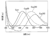
この光学素子10を、駆動回路20に接続した。そして、電極12a及び12b間に30Vの交流電圧を印加し、電圧変化に伴う色変化を観察した。なお、この交流電圧の波形は矩形波とし、周波数は30Hzとした。結果を図22に示す。
図22は、電圧変化に伴う色変化の他の例を示すグラフである。図中、横軸は波長を示し、縦軸は吸光度(任意単位)を示している。また、曲線COFFは電圧無印加状態における吸収スペクトルを示している。そして、曲線CON(0)、CON(30)及びCON(90)は、それぞれ、電圧を印加した直後、電圧印加を開始してから30秒経過後、及び電圧印加を開始してから90秒経過後における吸収スペクトルを示している。
(例4)
本例では、図21に示す光学素子10を、以下の方法により製造した。
ITO電極12a及び12bがそれぞれ設けられた透明な無アルカリガラス基板11a及び11bを2枚準備した。各ガラス基板の厚さは、0.7mmであった。
本例では、図21に示す光学素子10を、以下の方法により製造した。
ITO電極12a及び12bがそれぞれ設けられた透明な無アルカリガラス基板11a及び11bを2枚準備した。各ガラス基板の厚さは、0.7mmであった。
次に、電極12aにラビング処理を施した。次いで、電極12a上に、ソルバトクロミック色素を側鎖に有している高分子を含んだ液を30nmの厚さにスピナーによりキャストした。更に、この塗膜にラビング処理を施すことにより、色素層13SDを得た。この高分子としては、下記化学式に示す化合物を使用した。続いて、基板11aの上記主面の周縁部に、シール層15として使用するエポキシ接着剤をディスペンスした。

次に、電極12b上に、ポリイミドを70nmの厚さにスピナーによりキャストし、塗膜にラビング処理を施すことにより、絶縁層17bを形成した。ポリイミドとしては、日本合成ゴム社製のAL-1051を使用した。そして、絶縁層17b上に、直径が10μmの樹脂製スペーサボールを散布した。
その後、基板11a及び11bを、絶縁層17a及び17bが向き合うように及びラビング方向が平行になるように貼り合せ、エポキシ接着剤を硬化させた。これにより、空セルを得た。
次に、Merck社製のネマチック液晶材料を、液晶相の状態で空セルへ真空注入して、液晶層13LCを形成した。ネマチック液晶材料としては、誘電率異方性Δεが20であり、屈折率異方性Δnが0.15であるものを使用した。
空セルの注入口を封止した後、基板11a上に反射フィルム16を貼りつけた。以上のようにして、図21に示す光学素子10を完成した。
この光学素子10を、駆動回路20に接続した。そして、電極12a及び12b間に交流電圧を印加し、電圧変化に伴う色変化を観察した。なお、この交流電圧の波形は矩形波とし、周波数は30Hzとした。
その結果、この光学素子10は、電圧無印加状態(0V)においては赤色を表示し、印加電圧を15Vとしたときに緑色を表示した。
(例5)
本例では、図18及び図19を参照しながら説明した光学素子を、以下の方法により製造した。
本例では、図18及び図19を参照しながら説明した光学素子を、以下の方法により製造した。
まず、ホウケイ酸ソーダガラスの熱処理とそれに続く酸処理とにより、厚さが3μmであり、細孔径が1μmの多孔質ガラスビーズ13Pを作製した。この多孔質ガラスビーズにReichardt色素のエタノール溶液を含浸させて、Reichardt色素を細孔の壁面に固定化した。
このようにして得られた粒子を、ITO電極がその表面に設けられた透明な2枚のガラス基板とシール層とからなるセルの中に封入した。ガラス基板としては、厚さが0.7mmの無アルカリガラス基板を使用した。
その後、セルの中に、Merck社製のネマチック液晶材料を等方相の状態で真空注入した。ネマチック液晶材料としては、誘電率異方性Δεが15であり、屈折率異方性Δnが0.18であるものを使用した。
セルの注入口を封止した後、一方の基板上に反射フィルム16を貼りつけた。以上のようにして、図18及び図19を参照しながら説明した光学素子を完成した。
この光学素子10を、駆動回路20に接続した。そして、電極12a及び12b間に交流電圧を印加し、電圧変化に伴う色変化を観察した。なお、この交流電圧の波形は矩形波とし、周波数は30Hzとした。
その結果、この光学素子10は、電圧無印加状態(0V)においては赤紫色を表示し、印加電圧を50Vとしたときに黄緑色を表示した。
更なる利益及び変形は、当業者には容易である。それゆえ、本発明は、そのより広い側面において、ここに記載された特定の記載や代表的な態様に限定されるべきではない。従って、添付の請求の範囲及びその等価物によって規定される本発明の包括的概念の真意又は範囲から逸脱しない範囲内で、様々な変形が可能である。
Claims (20)
- 誘電率異方性を有する材料とソルバトクロミック色素とを含んだ光学的可変層と、
前記光学的可変層に電圧を印加する第1及び第2電極と
を具備した光学素子。 - 前記誘電率異方性を有する材料は液晶材料である請求項1に記載の光学素子。
- 前記ソルバトクロミック色素は固定化されている請求項1に記載の光学素子。
- 前記ソルバトクロミック色素は多孔質体に支持されている請求項3に記載の光学素子。
- 前記ソルバトクロミック色素は化学結合によって固定化されている請求項3に記載の光学素子。
- 前記ソルバトクロミック色素は高分子材料の主鎖又は側鎖に組み込まれている請求項5に記載の光学素子。
- 前記ソルバトクロミック色素は配向している請求項3に記載の光学素子。
- 前記ソルバトクロミック色素の吸収軸は前記光学的可変層の主面に平行である請求項7に記載の光学素子。
- 前記誘電率異方性を有する材料は液晶材料である請求項7に記載の光学素子。
- 前記光学的可変層の主面と接し、前記液晶材料の配向を制御するように構成された配向膜を更に具備した請求項7に記載の光学素子。
- 前記ソルバトクロミック色素の基底状態又は励起状態における電気双極子モーメントの方向は、前記配向膜が前記液晶材料を配向させる配向方向に対して平行であり、前記第1及び第2電極間に電圧を印加した場合に生じる電場の向きに対して垂直である請求項10に記載の光学素子。
- 前記ソルバトクロミック色素の基底状態又は励起状態における電気双極子モーメントの方向は、前記配向膜が前記液晶材料を配向させる配向方向に対して垂直であり、前記第1及び第2電極間に電圧を印加した場合に生じる電場の向きに対して平行である請求項10に記載の光学素子。
- 前記ソルバトクロミック色素の少なくとも一部は前記誘電率異方性を有する材料と混合されている請求項1に記載の光学素子。
- 前記誘電率異方性を有する材料は液晶材料である請求項13に記載の光学素子。
- 前記ソルバトクロミック色素は有機材料である請求項1に記載の光学素子。
- 前記ソルバトクロミック色素は分子内電荷移動構造を有している請求項1に記載の光学素子。
- 請求項1に記載の光学素子と、前記第1及び第2電極間に駆動電圧を印加する駆動回路とを含んだ表示装置。
- 前記誘電率異方性を有する材料は液晶材料である請求項17に記載の表示装置。
- 前記ソルバトクロミック色素は固定化されている請求項17に記載の表示装置。
- 前記ソルバトクロミック色素の少なくとも一部は前記誘電率異方性を有する材料と混合されている請求項17に記載の表示装置。
Priority Applications (1)
| Application Number | Priority Date | Filing Date | Title |
|---|---|---|---|
| US13/111,591 US8531644B2 (en) | 2008-11-19 | 2011-05-19 | Optical device and display |
Applications Claiming Priority (2)
| Application Number | Priority Date | Filing Date | Title |
|---|---|---|---|
| JP2008295851A JP5238462B2 (ja) | 2008-11-19 | 2008-11-19 | 光学素子及び表示装置 |
| JP2008-295851 | 2008-11-19 |
Related Child Applications (1)
| Application Number | Title | Priority Date | Filing Date |
|---|---|---|---|
| US13/111,591 Continuation US8531644B2 (en) | 2008-11-19 | 2011-05-19 | Optical device and display |
Publications (1)
| Publication Number | Publication Date |
|---|---|
| WO2010058799A1 true WO2010058799A1 (ja) | 2010-05-27 |
Family
ID=42198238
Family Applications (1)
| Application Number | Title | Priority Date | Filing Date |
|---|---|---|---|
| PCT/JP2009/069577 Ceased WO2010058799A1 (ja) | 2008-11-19 | 2009-11-18 | 光学素子及び表示装置 |
Country Status (3)
| Country | Link |
|---|---|
| US (1) | US8531644B2 (ja) |
| JP (1) | JP5238462B2 (ja) |
| WO (1) | WO2010058799A1 (ja) |
Families Citing this family (1)
| Publication number | Priority date | Publication date | Assignee | Title |
|---|---|---|---|---|
| WO2026004665A1 (ja) * | 2024-06-28 | 2026-01-02 | 富士フイルム株式会社 | 電気光学素子、及び、電気光学素子の製造方法 |
Citations (1)
| Publication number | Priority date | Publication date | Assignee | Title |
|---|---|---|---|---|
| JP2004233655A (ja) * | 2003-01-30 | 2004-08-19 | Fuji Photo Film Co Ltd | 画像表示素子、画像表示装置及び化合物の製造方法 |
Family Cites Families (3)
| Publication number | Priority date | Publication date | Assignee | Title |
|---|---|---|---|---|
| JP5103730B2 (ja) | 2005-06-03 | 2012-12-19 | 富士ゼロックス株式会社 | 表示方法、並びに、これを用いた表示媒体及び表示素子 |
| JP5034271B2 (ja) | 2006-03-06 | 2012-09-26 | 富士ゼロックス株式会社 | 表示媒体の表示方法、及び表示装置 |
| JP2007279163A (ja) | 2006-04-03 | 2007-10-25 | Fuji Xerox Co Ltd | 表示方法、表示媒体、及び表示素子 |
-
2008
- 2008-11-19 JP JP2008295851A patent/JP5238462B2/ja not_active Expired - Fee Related
-
2009
- 2009-11-18 WO PCT/JP2009/069577 patent/WO2010058799A1/ja not_active Ceased
-
2011
- 2011-05-19 US US13/111,591 patent/US8531644B2/en not_active Expired - Fee Related
Patent Citations (1)
| Publication number | Priority date | Publication date | Assignee | Title |
|---|---|---|---|---|
| JP2004233655A (ja) * | 2003-01-30 | 2004-08-19 | Fuji Photo Film Co Ltd | 画像表示素子、画像表示装置及び化合物の製造方法 |
Non-Patent Citations (2)
| Title |
|---|
| HIROKI IWANAGA ET AL.: "Oligothiophene dyes for guest-host liquid crystal displays", LIQUID CRYSTALS, vol. 27, no. 1, 2000, pages 115 - 123 * |
| LARS-OLOF PALSSON ET AL.: "ORIENTATION AND SOLVATOCHROMISM OF DYES IN LIQUID CRYSTAL", MOL. CRYST. LIQ. CRYST., vol. 402, 2003, pages 43(279) - 53(289) * |
Also Published As
| Publication number | Publication date |
|---|---|
| US20110279756A1 (en) | 2011-11-17 |
| US8531644B2 (en) | 2013-09-10 |
| JP2010122454A (ja) | 2010-06-03 |
| JP5238462B2 (ja) | 2013-07-17 |
Similar Documents
| Publication | Publication Date | Title |
|---|---|---|
| US7864287B2 (en) | Liquid crystal composition, liquid crystal optical device, and method of producing liquid crystal optical device | |
| EP3323014B1 (en) | Device for the regulation of light transmission | |
| CN102231027B (zh) | 一种采用波纹形电极的透反蓝相液晶显示器 | |
| JPH09166780A (ja) | 反射型液晶表示装置 | |
| KR19980063717A (ko) | 반사형 액정표시소자 | |
| KR20020077439A (ko) | 액정 디스플레이 라미네이트와 그 제조방법 | |
| JPH11183937A (ja) | 液晶光学スイッチ素子、カラーシャッターおよびカラー画像表示装置 | |
| TW201033713A (en) | Reflective color-changing liquid crystal display | |
| JP2005234204A (ja) | 液晶表示装置 | |
| JPH08297280A (ja) | 液晶表示装置 | |
| US6950171B2 (en) | Liquid crystal color switch and method of manufacture | |
| JPH0367219A (ja) | 液晶表示素子 | |
| KR20140070478A (ko) | 주기적인 마이크로 패턴을 갖는 fpr | |
| JP3679869B2 (ja) | 液晶マイクロカプセルおよびそれを用いた液晶表示素子 | |
| JP2010262055A (ja) | 表示素子および表示装置 | |
| JP5238462B2 (ja) | 光学素子及び表示装置 | |
| JP2000178557A (ja) | 液晶組成物及び液晶光変調素子 | |
| JP4978391B2 (ja) | 反射型液晶表示媒体 | |
| WO1992014185A1 (en) | Liquid crystal display device, and manufacture and application thereof | |
| JPH08106087A (ja) | 反射型液晶表示装置 | |
| JP2003149632A (ja) | 液晶表示装置、及び、そのカラーフィルタ | |
| JPH11258638A (ja) | ゲストホスト型液晶表示装置 | |
| JP2002202526A (ja) | 液晶表示素子 | |
| JPH0519231A (ja) | Stn型液晶表示装置 | |
| JP2001188258A (ja) | 液晶表示素子 |
Legal Events
| Date | Code | Title | Description |
|---|---|---|---|
| 121 | Ep: the epo has been informed by wipo that ep was designated in this application |
Ref document number: 09827580 Country of ref document: EP Kind code of ref document: A1 |
|
| NENP | Non-entry into the national phase |
Ref country code: DE |
|
| 122 | Ep: pct application non-entry in european phase |
Ref document number: 09827580 Country of ref document: EP Kind code of ref document: A1 |