WO2010052771A1 - 電子部品ハンドリング装置および電子部品移送方法 - Google Patents
電子部品ハンドリング装置および電子部品移送方法 Download PDFInfo
- Publication number
- WO2010052771A1 WO2010052771A1 PCT/JP2008/070133 JP2008070133W WO2010052771A1 WO 2010052771 A1 WO2010052771 A1 WO 2010052771A1 JP 2008070133 W JP2008070133 W JP 2008070133W WO 2010052771 A1 WO2010052771 A1 WO 2010052771A1
- Authority
- WO
- WIPO (PCT)
- Prior art keywords
- test
- tray
- unit
- loader
- unloader
- Prior art date
- Legal status (The legal status is an assumption and is not a legal conclusion. Google has not performed a legal analysis and makes no representation as to the accuracy of the status listed.)
- Ceased
Links
Images





Classifications
-
- G—PHYSICS
- G01—MEASURING; TESTING
- G01R—MEASURING ELECTRIC VARIABLES; MEASURING MAGNETIC VARIABLES
- G01R31/00—Arrangements for testing electric properties; Arrangements for locating electric faults; Arrangements for electrical testing characterised by what is being tested not provided for elsewhere
- G01R31/28—Testing of electronic circuits, e.g. by signal tracer
- G01R31/2851—Testing of integrated circuits [IC]
- G01R31/2893—Handling, conveying or loading, e.g. belts, boats, vacuum fingers
-
- G—PHYSICS
- G01—MEASURING; TESTING
- G01R—MEASURING ELECTRIC VARIABLES; MEASURING MAGNETIC VARIABLES
- G01R31/00—Arrangements for testing electric properties; Arrangements for locating electric faults; Arrangements for electrical testing characterised by what is being tested not provided for elsewhere
- G01R31/28—Testing of electronic circuits, e.g. by signal tracer
- G01R31/2851—Testing of integrated circuits [IC]
- G01R31/2855—Environmental, reliability or burn-in testing
- G01R31/286—External aspects, e.g. related to chambers, contacting devices or handlers
- G01R31/2865—Holding devices, e.g. chucks; Handlers or transport devices
- G01R31/2867—Handlers or transport devices, e.g. loaders, carriers, trays
Definitions
- the present invention relates to an electronic component handling apparatus for transferring a plurality of electronic components in order to test an electronic component such as an IC device, and a method for transferring a plurality of electronic components in such an electronic component handling apparatus.
- an electronic part testing apparatus for testing the finally manufactured electronic parts is required.
- a large number of IC devices are accommodated in a test tray and conveyed by an electronic component handling apparatus called a handler, and external terminals of the respective IC devices are connected to sockets provided on the test head. Electrically contact the terminals and have the test main unit (tester) perform the test.
- tester test main unit
- the handler is an apparatus that transfers the IC device before the test between the trays, that is, a loader device that picks up the IC device before the test from the supply tray (customer tray) and places the IC device on the test tray (test tray). Loader pick and place) and an apparatus for transferring a tested IC device between trays, that is, an unloader apparatus (unloader) for picking up a tested IC device from the test tray and placing it on a sorting tray (customer tray) Pick and place).
- a loader device that picks up the IC device before the test from the supply tray (customer tray) and places the IC device on the test tray (test tray).
- Loader pick and place an apparatus for transferring a tested IC device between trays, that is, an unloader apparatus (unloader) for picking up a tested IC device from the test tray and placing it on a sorting tray (customer tray) Pick and place).
- the loader pick and place is used only for loading the IC device before the test, and the unloader pick and place is used only for unloading the tested IC device. Therefore, at the time of handler lot start, only the loader pick and place operates, and the unloader pick and place does not operate. Further, after all the IC devices before the test are mounted on the test tray, the loader pick and place does not operate.
- the number of IC devices to be measured simultaneously has been increased to improve the efficiency of testing.
- the number of IC devices mounted on the test tray is also increasing, but as the number increases, the time from the lot start to the first test becomes longer, and the throughput of the electronic component testing apparatus decreases accordingly. There is a problem of doing.
- the tested IC devices mounted on the test tray are sorted into the customer tray, the same problem occurs because the number of IC devices to be sorted is large.
- the present invention has been made in view of such a situation, and an object thereof is to provide an electronic component handling apparatus and an electronic component transfer method capable of improving the transfer efficiency of electronic components between trays.
- the present invention transfers a pre-test electronic component from a supply tray to a test tray, and transfers a tested electronic component from the test tray to a sorting tray.
- An electronic component handling device comprising a transport device for transporting to a section, wherein the unloader device also transports an electronic component before testing from a supply tray set in the unloader section to a test tray.
- An electronic component handling device is provided (Invention 1).
- the said loader apparatus when the said loader apparatus transfers the electronic component before a test from a 1st supply tray to a 1st test tray, the said unloader apparatus is a 2nd electronic component before a test. It is preferable to transfer from the supply tray to the second test tray (Invention 2).
- the transfer device when the second test tray becomes full before the first test tray, the transfer device becomes full later in the loader unit.
- the second test tray is transported to the loader section and then transported to the test section side (Invention 4).
- the unloader device stops the transfer of the electronic components to the second test tray, and the transport The apparatus transports the second test tray to the loader section after transporting the first test tray filled with the loader section to the test section side, and the loader apparatus is an electronic component. May be transferred to an empty portion of the second test tray (Invention 5).
- the electronic component before the test is transferred from the supply tray to the test tray until the test tray on which the tested electronic component is mounted is carried out from the test unit side to the unloader unit. It is preferable to perform the operation of the unloader device to be transported to (Invention 6). According to this invention, the unloader device can be used for loading to the maximum extent until the unloader device performs the unloading operation.
- the present invention provides a loader device for transferring an electronic component before the test from the supply tray to the test tray, an unloader device for transferring the tested electronic component from the test tray to the sorting tray, and the test tray.
- a loader unit that operates the loader device to a test unit that performs an electronic component test
- a transfer device that transfers the tester unit to the unloader unit that operates the unloader device
- the unloader unit to the loader unit.
- An electronic component handling apparatus provided with the electronic component handling apparatus, wherein the loader device also transfers a tested electronic component from a test tray to a sorting tray set in the loader unit. (Invention 7).
- the said unloader apparatus and the said loader apparatus transfer the tested electronic component which concerns on a mutually different test result from the tray for a test to the tray for each test result ( Invention 8).
- the unloader device transfers only the tested electronic components related to the predetermined test result from the test tray on which the tested electronic components are mounted to the test result sorting tray.
- the transport device transports the test tray in which the tested electronic components relating to the test results other than the predetermined test result remain from the unloader unit to the loader unit, It is preferable to transfer a tested electronic component related to a test result other than the predetermined test result from the test tray to the sorting tray for the test result (Invention 9).
- the present invention relates to a loader device that transfers an electronic component before the test from the supply tray to the test tray, an unloader device that transfers the tested electronic component from the test tray to the sorting tray, and the test tray.
- a loader unit that operates the loader device to a test unit that performs an electronic component test a transfer device that transfers the tester unit to the unloader unit that operates the unloader device, and the unloader unit to the loader unit.
- a method for transferring an electronic component before a test in an electronic component handling apparatus provided, wherein the loader device transfers an electronic component before a test from a supply tray set in the loader unit to a test tray.
- the unloader device also transfers electronic components before the test from the supply tray set in the unloader unit to the test tray.
- the present invention relates to a loader device that transfers an electronic component before the test from the supply tray to the test tray, an unloader device that transfers the tested electronic component from the test tray to the sorting tray, and a test tray.
- a loader unit that operates the loader device to a test unit that performs an electronic component test a transfer device that transfers the tester unit to the unloader unit that operates the unloader device, and the unloader unit to the loader unit.
- a method of transferring an electronic component before a test in an electronic component handling device provided, wherein the loader device transfers the electronic component before the test from a first supply tray to a first test tray.
- the apparatus also transfers the pre-test electronic components from the second supply tray to the second test tray, and when the first test tray is full,
- the apparatus and the unloader device stop the transfer of the electronic components to the test tray, and the transport device transports the first test tray to the test unit side and transfers the second test tray to the loader.
- the loader device transfers the electronic component to an empty portion of the second test tray (Invention 11).
- the transfer device when the second test tray becomes full before the first test tray, the transfer device becomes full later in the loader unit.
- the second test tray is transported to the loader section and then transported to the test section side (Invention 12).
- the present invention relates to a loader device that transfers electronic components before the test from the supply tray to the test tray, an unloader device that transfers the tested electronic components from the test tray to the sorting tray, and the test tray.
- a loader unit that operates the loader device to a test unit that performs an electronic component test a transfer device that transfers the tester unit to the unloader unit that operates the unloader device, and the unloader unit to the loader unit.
- a method of transferring an electronic component before a test in an electronic component handling device provided, wherein the loader device transfers the electronic component before the test from a first supply tray to a first test tray.
- the apparatus also transfers electronic parts before testing from the second supply tray to the second testing tray, and a predetermined number of electronic parts are mounted on the second testing tray.
- the unloader device stops the transfer of the electronic component to the second test tray, and the transport device transports the first test tray that is full in the loader unit to the test unit side. Then, the second test tray is transported to the loader unit, and the loader device transports the electronic component to an empty part of the second test tray.
- the present invention provides a loader device for transferring an electronic component before the test from the supply tray to the test tray, an unloader device for transferring the tested electronic component from the test tray to the sorting tray, and the test tray.
- a loader unit that operates the loader device to a test unit that performs an electronic component test
- a transfer device that transfers the tester unit to the unloader unit that operates the unloader device
- the unloader unit to the loader unit.
- a method for transferring a tested electronic component in an electronic component handling apparatus provided, wherein the unloader device transfers the tested electronic component from a test tray to a sorting tray set in the unloader unit.
- the loader device also transfers a tested electronic component from the test tray to a sorting tray set in the loader unit.
- the present invention provides a loader device for transferring an electronic component before a test from a supply tray to a test tray, an unloader device for transferring a tested electronic component from a test tray to a sorting tray, and a test tray.
- a loader unit that operates the loader device to a test unit that performs an electronic component test, a transfer device that transfers the tester unit to the unloader unit that operates the unloader device, and the unloader unit to the loader unit.
- a method for transporting a tested electronic component in an electronic component handling apparatus provided, wherein the unloader device only receives a tested electronic component related to a predetermined test result from a test tray on which the tested electronic component is mounted.
- test tray is transported from the unloader unit to the loader unit, and the loader device only tests the tested electronic components related to the test results other than the predetermined test result from the test tray.
- an electronic component transfer method characterized by transferring to a result sorting tray (Invention 15).
- the loader device or the unloader device can be operated efficiently, the transfer efficiency of the electronic components between the trays can be improved, and as a result, the throughput of the electronic component test device can be improved.
- FIG. 1 is an overall side view of an IC device test apparatus including a handler according to an embodiment of the present invention.
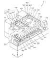
- FIG. 2 is a perspective view of a handler according to an embodiment of the present invention.
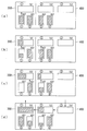
- FIG. 3-A is an explanatory diagram showing an example of a method for transferring a pre-test IC device.
- FIG. 3-B is an explanatory diagram showing an example of a method for transferring a pre-test IC device.
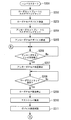
- FIG. 4 is a flowchart illustrating an example of a method for transferring a pre-test IC device.
- FIG. 5-A is an explanatory diagram showing another example of a method for transferring a pre-test IC device.
- FIG. 5B is an explanatory diagram showing another example of the method for transferring the pre-test IC device.
- FIG. 6A is a flowchart showing another example of the method for transferring the pre-test IC device.
- FIG. 6-B is a flowchart showing another example of the method for transferring the pre-test IC device.
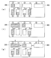
- FIG. 7A is an explanatory diagram showing an example of a method for transferring a tested IC device.
- FIG. 7-B is an explanatory diagram showing an example of a method for transferring a tested IC device.
- the IC device test apparatus 10 includes a handler 1, a test head 5, and a test main apparatus 6.
- the handler 1 sequentially carries IC devices (an example of electronic components) to be tested to a socket provided in the test head 5, classifies the IC devices that have been tested according to the test results, and stores them in a predetermined tray. To do.
- the socket provided in the test head 5 is electrically connected to the test main device 6 through the cable 7, and the IC device detachably attached to the socket is connected to the test main device 6 through the cable 7.
- the test is performed by a test electrical signal from the test main device 6.
- a control device for mainly controlling the handler 1 is built in the lower part of the handler 1, but a space portion 8 is provided in part.
- a test head 5 is replaceably disposed in the space portion 8, and an IC device can be attached to a socket on the test head 5 through a through hole formed in the handler 1.
- the handler 1 is an apparatus for testing an IC device as an electronic component to be tested in a temperature state (high temperature) higher than normal temperature or a low temperature state (low temperature).
- the handler 1 is as shown in FIG.
- the chamber 100 includes a constant temperature bath 101, a test chamber 102, and a heat removal bath 103.
- the upper part of the test head 5 shown in FIG. 1 is inserted into the test chamber 102, where the IC device is tested.
- the handler 1 of the present embodiment stores an IC device to be tested from now on, a device storage unit 200 that classifies and stores tested IC devices, and is sent from the device storage unit 200.
- a large number of IC devices before the test are stored in the customer tray KST, and in that state, are supplied to the IC storage unit 200 of the handler 1 shown in FIG. 2, and are transported in the handler 1 from the customer tray KST.
- the IC device is transferred to the test tray TST. Inside the handler 1, the IC device moves while being placed on the test tray TST, is subjected to high temperature or low temperature stress, and is tested (inspected) for proper operation, according to the test result. being classified.
- the inside of the handler 1 will be described in detail individually.
- the device storage unit 200 includes a pre-test device stocker 201 that stores pre-test IC devices, and a tested device stocker 202 that stores IC devices classified according to the test results. Is provided.
- pre-test device stocker 201 a customer tray KST storing IC devices (pre-test IC devices) to be tested is stacked and held.
- the tested device stocker 202 holds and stacks customer trays KST storing IC devices (tested IC devices) classified after the test.
- the tested device stocker 202 can be used as the pre-test device stocker 201 and vice versa.
- the device substrate 105 in the loader unit 300 has three pairs of windows 306 and 306 that are arranged so that the customer tray KST for supply faces the upper surface of the device substrate 105. .
- a tray set elevator (not shown) for raising and lowering the customer tray KST is provided below each window 306.
- a plate that supports the customer tray KST is referred to as a loader set plate.
- a tray transfer arm 205 that is movable in the X-axis direction and the Z-axis direction is provided between the device storage unit 200 and the apparatus substrate 105.
- the tray transfer arm 205 moves in the Z-axis direction to take out the customer tray KST from the pre-test device stocker 201, and then moves in the X-axis direction to deliver the customer tray KST to a predetermined tray set elevator.
- the tray set elevator raises the received customer tray KST and makes it appear in the window 306 of the loader unit 300.
- the IC devices to be tested stored in the customer tray KST are once transferred to the precursor 305 by the XY transport device 304, where the mutual positions of the IC devices to be tested are determined.
- the IC device under test transferred to the precursor 305 is reloaded onto the test tray TST stopped at the loader unit 300 by the XY transport device 304 again.
- an XY transfer device (hereinafter also referred to as “loader pick and place” or “loader P & P”) 304 that reloads IC devices to be tested from the customer tray KST to the test tray TST
- Two rails 301 installed on the upper part of the substrate 105, and a movable arm 302 that can reciprocate between the test tray TST and the customer tray KST by the two rails 301 (this direction is defined as the Y direction).
- a movable head 303 supported by the movable arm 302 and movable in the X direction along the movable arm 302.
- a plurality of suction pads 307 are mounted downward on the movable head 303 of the loader pick-and-place 304.
- the suction pads 307 move while sucking air, so that the IC device under test is moved from the customer tray KST. And the IC device under test is transferred to the test tray TST.
- four suction pads 307 are arranged in parallel with the movable head 303 in the X-axis direction, and a maximum of four IC devices to be tested can be transferred to the test tray TST at a time.
- test tray TST is loaded into the chamber 100 after the IC devices to be tested are loaded by the loader unit 300, and each IC device to be tested is tested while being mounted on the test tray TST.
- the chamber 100 is provided with a thermostatic chamber 101 that applies a desired high or low temperature thermal stress to the IC device under test loaded on the test tray TST, and the thermostatic chamber 101 is subjected to the thermal stress.
- a test chamber 102 in which an IC device under test is mounted in a socket on a test head, and a heat removal tank 103 that removes applied thermal stress from the IC device under test in the test chamber 102 Has been.
- the IC device under test when a high temperature is applied in the thermostatic chamber 101, the IC device under test is cooled by blowing to return to room temperature, and when a low temperature is applied in the thermostatic chamber 101, the IC device under test is heated with warm air. Or, it is heated with a heater or the like and returned to a temperature at which condensation does not occur. Then, the IC device to be tested after the heat removal is carried out to the unloader unit 400.
- a vertical transfer device is provided, and a plurality of test trays TST stand by while being supported by the vertical transfer device until the test chamber 102 becomes empty. Mainly, during this standby, high or low temperature thermal stress is applied to the IC device under test.
- the test head 5 is disposed at the lower center of the test chamber 102, and the test tray TST is carried on the test head 5. In this case, all the IC devices stored in the test tray TST are brought into electrical contact with the test head 5 to perform the test.
- the test tray TST is removed from heat in the heat removal tank 103, and after the temperature of the tested IC device is returned to room temperature, it is carried out to the unloader unit 400 shown in FIG.
- an inlet opening for feeding the test tray TST from the apparatus substrate 105 to the upper part of the constant temperature bath 101 and the heat removal tank 103, and for sending the test tray TST to the apparatus substrate 105.
- Each of the outlet openings is formed.
- a test tray transfer device 108 for taking in and out the test tray TST from these openings is mounted. These conveying devices 108 are constituted by rotating rollers, for example.
- the test tray TST unloaded from the heat removal tank 103 is transferred to the unloader unit 400 by the test tray transfer device 108 provided on the apparatus substrate 105.
- a plurality of inserts are attached to the test tray TST.
- the insert is formed with an IC device storage portion for storing an IC device.
- the IC device is loaded on the test tray TST.
- a transport roller or the like is used as a means for transporting the test tray TST inside the chamber 100.
- the unloader unit 400 shown in FIG. 2 may also be referred to as an XY transport device (hereinafter “unloader pick and place” or “unloader P & P”) having the same structure as the XY transport device 304 provided in the loader unit 300. ) 404 is provided, and by this unloader pick and place 404, the tested IC devices are transferred from the test tray TST carried to the unloader unit 400 to the customer tray KST.
- unloader pick and place or “unloader P & P”
- the device substrate 105 in the unloader unit 400 has two pairs of windows 406 and 406 arranged so that the customer tray KST conveyed to the unloader unit 400 faces the upper surface of the device substrate 105. It has been opened. Under each window 406, a tray set elevator (not shown) for raising and lowering the customer tray KST is provided. In this tray set elevator, a plate that supports the customer tray KST is referred to as an unloader set plate.
- the tray set elevator is lowered by placing a sorting customer tray KST (sorted tray) in which tested IC devices are sorted and stored.
- the tray transfer arm 205 shown in FIG. 2 receives the sorted tray from the lowered tray set elevator, moves in the X-axis direction and the Z-axis direction, and stores the sorted tray in the predetermined tested device stocker 202.
- a plurality of customer trays KST satisfying pre-test IC devices are stacked on the two pre-test device stockers 201 in advance.
- step S101 When the handler is started (step S101), as shown in FIG. 3-A (a), the first customer tray KST is set on the loader set plate (step S102), and the loader P & P 304 is moved to the first customer tray KST. Are sequentially picked up and placed on the first test tray TST located in the loader unit 300 (step S103).
- the second customer tray KST is set on the unloader set plate (step S104), and the unloader P & P 404 sequentially loads the pre-test IC devices from the second customer tray KST.
- the pickup is picked up and placed on the second test tray TST located in the unloader unit 400 (step S105).
- the loader P & P 304 moves the IC device before the test from the third customer tray KST. Is transferred to the test tray TST.
- the handler determines whether or not the test tray (loader test tray) TST located in the loader unit 300 is filled with pre-test IC devices (step S106). If the loader test tray TST is not full (step S106-No), it is determined whether the test tray (unloader test tray) TST located in the unloader unit 400 is full with the pre-test IC device (step S107). . If the unloader test tray is not full (No at Step S107), the process returns to Step S106.
- step S107 If the unloader test tray TST is full (step S107—Yes), the unloader P & P 404 stops the pre-test IC device transfer operation (step S108), and returns to step S106.
- step S106 when the loader test tray TST is full (step S106-Yes), the IC device transfer operation by the loader P & P 304 is stopped (step S109), and the unloader P & P 404 is also displayed. The IC device transfer operation is stopped (step S110). Then, as shown in FIGS. 3-A (d) to 3-B (e), the test tray transport device 108 transports each test tray TST by one step (step S111).
- test tray transport device 108 transports the first test tray TST to the thermostatic chamber 101, transports the second test tray TST to the loader unit 300, and in the unloader unit 400, the side far from the loader unit 300 (hereinafter, “ The third test tray TST located in the unloader section 400R ”) is transported to the side closer to the loader section 300 (hereinafter referred to as“ unloader section 400L ”) in the unloader section 400, and the fourth test tray TST. From the heat removal tank 103 to the unloader section 400R. If the unloader test tray is already full in step S107, the test tray transport device 108 transports each test tray TST in the same manner as described above.
- step S112 the loader P & P 304 and the unloader P & P 404 resume the IC device transfer operation (step S112). Specifically, as shown in FIG. 3B (e), the loader P & P 304 transfers the pre-test IC device from the third customer tray KST to the empty portion of the second test tray TST. Further, the unloader P & P 404 transfers the pre-test IC device from the second customer tray KST to the third test tray TST.
- the handler determines whether or not the customer tray KST storing the pre-test IC device is lost in the unloader set plate (step S113). If the customer tray KST still exists (step S113-No), the process returns to step S106.
- step S106 when the second loader test tray is full (step S106—Yes), the IC device transfer operation by the loader P & P 304 is stopped (step S109). The IC device transfer operation by the unloader P & P 404 is stopped (step S110). Then, the test tray transport device 108 transports each test tray TST by one step (step S111). That is, the test tray transport device 108 transports the second test tray TST to the thermostatic chamber 101 and transports the third test tray TST to the loader unit 300.
- step S113 When the customer tray KST storing the pre-test IC device is lost on the unloader set plate (step S113—Yes), the unloader P & P 404 returns to the sort-only operation (step S114). Then, an empty customer tray KST is set on the unloader set plate (step S115). Note that the loader P & P 304 transfers the pre-test IC device from the fifth customer tray KST to the empty portion of the third test tray TST, and shifts to a normal operation.
- the loading operation by the unloader P & P 404 is preferably performed until the test tray TST (first test tray TST) on which the tested IC device is mounted is carried out from the heat removal tank 103 to the unloader unit 400.
- the unloader P & P 404 can be used for loading to the maximum extent until the unloader P & P 404 performs the unloading operation.
- the unloader P & P 404 performs the loading operation for two customer trays, but is not limited to this.
- the unloader P & P 404 since the unloader P & P 404 that is normally stopped at the time of loading performs a loading operation together with the loader P & P 304, the unloader P & P 404 can be used efficiently.
- the efficiency of transferring the pre-test IC device to the test tray TST can be improved, and as a result, the throughput of the IC device test apparatus 10 can be improved.
- Steps S201 to S205 are the same as steps S101 to S105 (FIGS. 3-A (a) to (c)) of the above embodiment.
- the handler determines whether a predetermined number of pre-test IC devices are stored in the test tray (unloader test tray) TST located in the unloader unit 400 (step S206).
- the predetermined number is preferably about 1/3 to 2/3 of the number of IC devices stored in the test tray TST, particularly preferably about 2/5 to 3/5, and more preferably about half.
- step S206—No If the predetermined number of pre-test IC devices are not stored in the unloader test tray TST (step S206—No), the above operation is continued as it is.
- step S206-Yes when a predetermined number of pre-test IC devices are stored in the unloader test tray TST (second test tray TST) (step S206-Yes), the unloader P & P 404 is used. The IC device transfer operation is stopped (step S207).
- the handler determines whether or not the loader test tray TST is full of pre-test IC devices (step S208). If the loader test tray TST is not full (step S208—No), the above operation is continued as it is. On the other hand, when the loader test tray TST is full (step S208—Yes), the transfer operation of the pre-test IC device by the loader P & P 304 is stopped (step S209).
- the test tray transport device 108 transports each test tray TST one step (step S210). That is, the test tray transport device 108 transports the first test tray TST to the thermostatic chamber 101, transports the second test tray TST to the loader unit 300, and the third test tray located in the unloader unit 400R. The TST is transported to the unloader unit 400L, and the fourth test tray TST is unloaded from the heat removal tank 103 to the unloader unit 400R.
- the loader P & P 304 and the unloader P & P 404 resume the IC device transfer operation (step S211). Specifically, as shown in FIG. 5-B (e), the loader P & P 304 transfers the pre-test IC device from the third customer tray KST to the empty portion of the second test tray TST. Further, the unloader P & P 404 transfers the pre-test IC device from the second customer tray KST to the third test tray TST.
- next steps S212 to S214 are the same as steps S113 to S115 (FIG. 3-B (f) to (g)) of the above embodiment. .
- the loading operation by the unloader P & P 404 is preferably performed until the test tray TST (first test tray TST) on which the tested IC device is mounted is carried out from the heat removal tank 103 to the unloader unit 400.
- the unloader P & P 404 performs the loading operation for two customer trays, but is not limited to this.
- the unloader P & P 404 since the unloader P & P 404 that is normally stopped at the time of loading performs a loading operation together with the loader P & P 304, the unloader P & P 404 can be used efficiently.
- the efficiency of transferring the pre-test IC device to the test tray TST can be improved, and as a result, the throughput of the IC device test apparatus 10 can be improved.
- test result A is a complete good product
- test result B is a complete defective product
- test result C is a good product, but some functions are slow
- test result D is a good product, but other functions Are sorted like things with slow speed.
- customer tray KST-1 customer tray KST-2 (located in the loader section 300), customer tray KST- 3, customer tray KST-4, customer tray KST-5, customer tray KST-6 (which is located in the unloader section 400).
- Customer tray KST-1 and customer tray KST-2 are set on the loader set plate, and customer tray KST-3, customer tray KST-4, customer tray KST-5 and customer tray KST-6 are set on the unloader set plate. Is done.
- the test result C is stored in the customer tray KST-1
- the test result D is stored in the customer tray KST-2
- the test result A is stored in the customer tray KST-3
- the test result A is stored in the customer tray KST-4.
- the test result B is sorted in the tray KST-5
- the tested IC device of the test result B is sorted in the customer tray KST-6.
- the IC device of the test result A is preferentially transferred to the customer tray KST-3, and when the customer tray KST-3 is full, it is switched to the customer tray KST-4 and transferred.
- the IC device of the test result B is preferentially transferred to the customer tray KST-5, and when the customer tray KST-5 is full, it is switched to the customer tray KST-6.
- the first test tray TST loaded with the tested IC device is unloaded from the heat removal tank 103 and positioned in the unloader unit 400L via the unloader unit 400R. Further, the second test tray TST on which the tested IC device is mounted is unloaded from the heat removal tank 103 and positioned in the unloader unit 400R. In each test tray TST, tested IC devices according to the test results A to D are mixedly mounted.
- the unloader P & P 404 picks up the tested IC device of the test result A from the first test tray TST and places it on the customer tray KST-3, picks up the tested IC device of the test result B and picks up the customer tray KST- 5 is placed.
- the tested IC device of the test result A and the tested IC device of the test result B Is transferred to the customer tray KST, the IC device transfer operation by the unloader P & P 404 is stopped.
- the tested IC device of the test result C and the tested IC device of the test result D are left in the first test tray TST.
- the test tray transport device 108 transports each test tray TST in one step. That is, the test tray transport device 108 transports the test tray TST located in the loader unit 300 to the thermostatic chamber 101, transports the first test tray TST located in the unloader unit 300L to the loader unit 300, The second test tray TST located in the unloader unit 300R is transported to the unloader unit 300L, and the third test tray TST is unloaded from the heat removal tank 103 to the unloader unit 400R.
- the loader P & P 304 transfers the tested IC device of the test result C from the first test tray TST to the customer tray KST-1, The IC device is transferred to the customer tray KST-2.
- the unloader P & P 404 transfers the tested IC device of the test result A from the second test tray TST to the customer tray KST-3, and the tested result B of the test result B is tested.
- the IC device is transferred to the customer tray KST-5.
- the destination of the tested IC device of the test result A is switched to the customer tray KST-4 and transferred, and the full customer tray KST-3 is transferred to the empty customer tray KST-3.
- tray KST-3 when the customer tray KST-5 is full, the transfer destination of the tested IC device of the test result B is switched to the customer tray KST-6, and the full customer tray KST-5 is transferred to the empty customer tray. Replace with KST-5.
- the customer tray KST (sorted tray) filled with the tested IC device is stored in a predetermined tested device stocker 202 by the tray set elevator and tray transfer arm 205, and the unloader at the position where the customer tray KST is located.
- An empty customer tray KST is set on the set plate or the loader set plate.
- the tested IC device of the test result C and the tested IC device of the test result D Are transferred to the customer tray KST, and from the test tray TST (second test tray TST) located in the unloader unit 400L, the tested IC devices of the test result A and the tested IC devices of the test result B are obtained.
- the IC device transfer operation by the loader P & P 304 and the unloader P & P 404 is stopped.
- the test tray transport device 108 transports each test tray TST in one step. That is, the test tray transport device 108 transports the first test tray TST located in the loader unit 300 to the thermostatic chamber 101, and the second test tray TST located in the unloader unit 300L to the loader unit 300. The third test tray TST located in the unloader unit 300R is transported to the unloader unit 300L, and the fourth test tray TST is unloaded from the heat removal tank 103 to the unloader unit 400R.
- the handler 1 repeats the above operation.
- the loader P & P 304 that is normally stopped at the time of unloading performs an unloading operation together with the unloader P & P 404, so that the loader P & P 304 can be used efficiently. It is possible to improve the transfer efficiency of the tested IC device from the TST to the customer tray KST, and thereby improve the throughput of the IC device testing apparatus 10.
- the electronic component transfer method and electronic component handling device of the present invention are useful for efficiently transferring electronic components and improving the throughput of the electronic component handling device.
Landscapes
- Engineering & Computer Science (AREA)
- Computer Hardware Design (AREA)
- Microelectronics & Electronic Packaging (AREA)
- General Engineering & Computer Science (AREA)
- Physics & Mathematics (AREA)
- General Physics & Mathematics (AREA)
- Environmental & Geological Engineering (AREA)
- Testing Of Individual Semiconductor Devices (AREA)
Abstract
試験前ICデバイスを供給用のカスタマトレイKSTからテストトレイTSTに移送するローダP&P304と、試験済ICデバイスをテストトレイTSTから仕分け用のカスタマトレイKSTに移送するアンローダP&P404と、テストトレイTSTをローダ部300~チャンバ100~アンローダ部400~ローダ部300間で搬送する搬送装置108とを備えたハンドラ1において、ローダP&P304が試験前ICデバイスを第1のカスタマトレイKSTから第1のテストトレイTSTに移送するときに、アンローダP&P404は、試験前ICデバイスを第2のカスタマトレイKSTから第2のテストトレイTSTに移送する。
Description
本発明は、ICデバイス等の電子部品を試験するために複数の電子部品を移送する電子部品ハンドリング装置、及びかかる電子部品ハンドリング装置において複数の電子部品を移送する方法に関するものである。
ICデバイス等の電子部品の製造課程においては、最終的に製造された電子部品を試験する電子部品試験装置が必要となる。かかる電子部品試験装置においては、ハンドラと称される電子部品ハンドリング装置により、多数のICデバイスをテストトレイに収納して搬送し、各ICデバイスの外部端子をテストヘッド上に設けられたソケットの接続端子に電気的に接触させ、試験用メイン装置(テスタ)に試験を行わせる。このようにしてICデバイスは試験され、少なくとも良品や不良品といったカテゴリに分類される。
ハンドラは、試験前のICデバイスをトレイ間で移送する装置、すなわち、試験前のICデバイスを供給用トレイ(カスタマトレイ)からピックアップして、試験用トレイ(テストトレイ)に載置するローダ装置(ローダピックアンドプレイス)と、試験済のICデバイスをトレイ間で移送する装置、すなわち、試験済のICデバイスをテストトレイからピックアップして、仕分け用トレイ(カスタマトレイ)に載置するアンローダ装置(アンローダピックアンドプレイス)とを備えている。
従来のハンドラでは、ローダピックアンドプレイスは、試験前のICデバイスのローディングだけに使用され、アンローダピックアンドプレイスは、試験済のICデバイスのアンローディングだけに使用されている。したがって、ハンドラのロットスタート時には、ローダピックアンドプレイスのみが動作し、アンローダピックアンドプレイスは動作しない。また、試験前のICデバイスを全てテストトレイに搭載した後は、ローダピックアンドプレイスは動作しない。
ところで、近年、同時に測定するICデバイスの数を増加させて、試験の効率化を図ることが行われている。これに伴って、テストトレイに搭載するICデバイスの数も増えているが、その数が増えると、ロットスタートから最初の試験までの時間が長くなり、その分、電子部品試験装置のスループットが低下するという問題がある。また、テストトレイに搭載された試験済のICデバイスをカスタマトレイに仕分けするときにも、仕分けすべきICデバイスの数が多いため、同様の問題が生じる。
本発明は、このような実状に鑑みてなされたものであり、トレイ間における電子部品の移送効率を向上させることのできる電子部品ハンドリング装置および電子部品移送方法を提供することを目的とする。
上記目的を達成するために、第1に本発明は、試験前の電子部品を供給用トレイから試験用トレイに移送するローダ装置と、試験済の電子部品を試験用トレイから仕分け用トレイに移送するアンローダ装置と、試験用トレイを、前記ローダ装置が動作するローダ部から電子部品の試験を実施するテスト部へ、前記テスト部から前記アンローダ装置が動作するアンローダ部へ、前記アンローダ部から前記ローダ部へ搬送する搬送装置とを備えた電子部品ハンドリング装置であって、前記アンローダ装置も、前記アンローダ部にセットされた供給用トレイから試験前の電子部品を試験用トレイに移送することを特徴とする電子部品ハンドリング装を提供する(発明1)。
上記発明(発明1)においては、前記ローダ装置が試験前の電子部品を第1の供給用トレイから第1の試験用トレイに移送するときに、前記アンローダ装置は試験前の電子部品を第2の供給用トレイから第2の試験用トレイに移送することが好ましい(発明2)。
上記発明(発明2)においては、前記第1の試験用トレイが満杯になると、前記アンローダ装置は電子部品の前記第2の試験用トレイへの移送を止め、前記搬送装置は、前記第1の試験用トレイを前記テスト部側に搬送するとともに、前記第2の試験用トレイを前記ローダ部に搬送し、前記ローダ装置は、電子部品を前記第2の試験用トレイの空き部分に移送するようにしてもよい(発明3)。
上記発明(発明3)において、前記第1の試験用トレイよりも前記第2の試験用トレイが先に満杯になった場合には、前記搬送装置は、前記ローダ部にて後で満杯になった第1の試験用トレイを前記テスト部側に搬送した後、前記第2の試験用トレイを前記ローダ部に搬送し、次いで前記テスト部側に搬送することが好ましい(発明4)。
上記発明(発明2)においては、前記第2の試験用トレイに所定数の電子部品が搭載されると、前記アンローダ装置は電子部品の前記第2の試験用トレイへの移送を止め、前記搬送装置は、前記ローダ部にて満杯になった第1の試験用トレイを前記テスト部側に搬送した後、前記第2の試験用トレイを前記ローダ部に搬送し、前記ローダ装置は、電子部品を前記第2の試験用トレイの空き部分に移送するようにしてもよい(発明5)。
上記発明(発明1)においては、試験済の電子部品を搭載した試験用トレイが前記テスト部側から前記アンローダ部に搬出されるまでの間、試験前の電子部品を供給用トレイから試験用トレイに移送する前記アンローダ装置の動作を行うことが好ましい(発明6)。かかる発明によれば、アンローダ装置がアンローディング動作を行うまで、アンローダ装置を最大限ローディングに利用することができる。
上記発明(発明1~6)によれば、ローディングの際に、ローダ装置だけでなく、アンローダ装置もローディング動作を行うため、供給用トレイから試験用トレイへの電子部品の移送効率を向上させることができる。
第2に本発明は、試験前の電子部品を供給用トレイから試験用トレイに移送するローダ装置と、試験済の電子部品を試験用トレイから仕分け用トレイに移送するアンローダ装置と、試験用トレイを、前記ローダ装置が動作するローダ部から電子部品の試験を実施するテスト部へ、前記テスト部から前記アンローダ装置が動作するアンローダ部へ、前記アンローダ部から前記ローダ部へ搬送する搬送装置とを備えた電子部品ハンドリング装置であって、前記ローダ装置も、試験用トレイから試験済の電子部品を前記ローダ部にセットされた仕分け用トレイに移送することを特徴とする電子部品ハンドリング装置を提供する(発明7)。
上記発明(発明7)において、前記アンローダ装置および前記ローダ装置は、互いに異なる試験結果に係る試験済の電子部品を、試験用トレイからそれぞれの試験結果用の仕分け用トレイに移送することが好ましい(発明8)。
上記発明(発明8)において、前記アンローダ装置は、試験済の電子部品を搭載した試験用トレイから、所定の試験結果に係る試験済の電子部品のみを、当該試験結果用の仕分け用トレイに移送し、前記搬送装置は、前記所定の試験結果以外の試験結果に係る試験済の電子部品が残された前記試験用トレイを、前記アンローダ部から前記ローダ部へ搬送し、前記ローダ装置は、前記試験用トレイから、前記所定の試験結果以外の試験結果に係る試験済の電子部品を、当該試験結果用の仕分け用トレイに移送することが好ましい(発明9)。
上記発明(発明7~9)によれば、アンローディングの際に、アンローダ装置だけでなく、ローダ装置もアンローディング動作を行うため、試験用トレイから仕分け用トレイへの電子部品の移送効率を向上させることができる。
第3に本発明は、試験前の電子部品を供給用トレイから試験用トレイに移送するローダ装置と、試験済の電子部品を試験用トレイから仕分け用トレイに移送するアンローダ装置と、試験用トレイを、前記ローダ装置が動作するローダ部から電子部品の試験を実施するテスト部へ、前記テスト部から前記アンローダ装置が動作するアンローダ部へ、前記アンローダ部から前記ローダ部へ搬送する搬送装置とを備えた電子部品ハンドリング装置における試験前の電子部品の移送方法であって、前記ローダ装置が、前記ローダ部にセットされた供給用トレイから試験前の電子部品を試験用トレイに移送するときに、前記アンローダ装置も、前記アンローダ部にセットされた供給用トレイから試験前の電子部品を試験用トレイに移送することを特徴とする電子部品移送方法を提供する(発明10)。
第4に本発明は、試験前の電子部品を供給用トレイから試験用トレイに移送するローダ装置と、試験済の電子部品を試験用トレイから仕分け用トレイに移送するアンローダ装置と、試験用トレイを、前記ローダ装置が動作するローダ部から電子部品の試験を実施するテスト部へ、前記テスト部から前記アンローダ装置が動作するアンローダ部へ、前記アンローダ部から前記ローダ部へ搬送する搬送装置とを備えた電子部品ハンドリング装置における試験前の電子部品の移送方法であって、前記ローダ装置が試験前の電子部品を第1の供給用トレイから第1の試験用トレイに移送するときに、前記アンローダ装置も試験前の電子部品を第2の供給用トレイから第2の試験用トレイに移送し、前記第1の試験用トレイが満杯になると、前記ローダ装置および前記アンローダ装置は電子部品の試験用トレイへの移送を止め、前記搬送装置は、前記第1の試験用トレイを前記テスト部側に搬送するとともに、前記第2の試験用トレイを前記ローダ部に搬送し、前記ローダ装置は、電子部品を前記第2の試験用トレイの空き部分に移送することを特徴とする電子部品移送方法を提供する(発明11)。
上記発明(発明11)において、前記第1の試験用トレイよりも前記第2の試験用トレイが先に満杯になった場合には、前記搬送装置は、前記ローダ部にて後で満杯になった第1の試験用トレイを前記テスト部側に搬送した後、前記第2の試験用トレイを前記ローダ部に搬送し、次いで前記テスト部側に搬送することが好ましい(発明12)。
第5に本発明は、試験前の電子部品を供給用トレイから試験用トレイに移送するローダ装置と、試験済の電子部品を試験用トレイから仕分け用トレイに移送するアンローダ装置と、試験用トレイを、前記ローダ装置が動作するローダ部から電子部品の試験を実施するテスト部へ、前記テスト部から前記アンローダ装置が動作するアンローダ部へ、前記アンローダ部から前記ローダ部へ搬送する搬送装置とを備えた電子部品ハンドリング装置における試験前の電子部品の移送方法であって、前記ローダ装置が試験前の電子部品を第1の供給用トレイから第1の試験用トレイに移送するときに、前記アンローダ装置も試験前の電子部品を第2の供給用トレイから第2の試験用トレイに移送し、前記第2の試験用トレイに所定数の電子部品が搭載されると、前記アンローダ装置は電子部品の前記第2の試験用トレイへの移送を止め、前記搬送装置は、前記ローダ部にて満杯になった第1の試験用トレイを前記テスト部側に搬送した後、前記第2の試験用トレイを前記ローダ部に搬送し、前記ローダ装置は、電子部品を前記第2の試験用トレイの空き部分に移送することを特徴とする電子部品移送方法を提供する(発明13)。
上記発明(発明10~13)によれば、ローディングの際に、ローダ装置だけでなく、アンローダ装置もローディング動作を行うため、供給用トレイから試験用トレイへの電子部品の移送効率を向上させることができる。
第6に本発明は、試験前の電子部品を供給用トレイから試験用トレイに移送するローダ装置と、試験済の電子部品を試験用トレイから仕分け用トレイに移送するアンローダ装置と、試験用トレイを、前記ローダ装置が動作するローダ部から電子部品の試験を実施するテスト部へ、前記テスト部から前記アンローダ装置が動作するアンローダ部へ、前記アンローダ部から前記ローダ部へ搬送する搬送装置とを備えた電子部品ハンドリング装置における試験済の電子部品の移送方法であって、前記アンローダ装置が、試験用トレイから試験済の電子部品を前記アンローダ部にセットされた仕分け用トレイに移送するときに、前記ローダ装置も、試験用トレイから試験済の電子部品を前記ローダ部にセットされた仕分け用トレイに移送することを特徴とする電子部品移送方法を提供する(発明14)。
第7に本発明は、試験前の電子部品を供給用トレイから試験用トレイに移送するローダ装置と、試験済の電子部品を試験用トレイから仕分け用トレイに移送するアンローダ装置と、試験用トレイを、前記ローダ装置が動作するローダ部から電子部品の試験を実施するテスト部へ、前記テスト部から前記アンローダ装置が動作するアンローダ部へ、前記アンローダ部から前記ローダ部へ搬送する搬送装置とを備えた電子部品ハンドリング装置における試験済の電子部品の移送方法であって、前記アンローダ装置は、試験済の電子部品を搭載した試験用トレイから、所定の試験結果に係る試験済の電子部品のみを、当該試験結果用の仕分け用トレイに移送し、前記搬送装置は、前記所定の試験結果以外の試験結果に係る試験済の電子部品が残された前記試験用トレイを、前記アンローダ部から前記ローダ部へ搬送し、前記ローダ装置は、前記試験用トレイから、前記所定の試験結果以外の試験結果に係る試験済の電子部品のみを、当該試験結果用の仕分け用トレイに移送することを特徴とする電子部品移送方法を提供する(発明15)。
上記発明(発明14,15)によれば、アンローディングの際に、アンローダ装置だけでなく、ローダ装置もアンローディング動作を行うため、試験用トレイから仕分け用トレイへの電子部品の移送効率を向上させることができる。
本発明によれば、ローダ装置またはアンローダ装置を効率良く動作させることができるため、トレイ間における電子部品の移送効率を向上させ、ひいては電子部品試験装置のスループットを向上させることができる。
1…ハンドラ(電子部品ハンドリング装置)
10…ICデバイス(電子部品)試験装置
108…テストトレイ搬送装置
300…ローダ部
304…ローダピックアンドプレイス(ローダ装置)
400…アンローダ部
404…アンローダピックアンドプレイス(アンローダ装置)
10…ICデバイス(電子部品)試験装置
108…テストトレイ搬送装置
300…ローダ部
304…ローダピックアンドプレイス(ローダ装置)
400…アンローダ部
404…アンローダピックアンドプレイス(アンローダ装置)
以下、本発明の実施形態を図面に基づいて説明する。
〔ハンドラの構成〕
まず、本実施形態に係る電子部品ハンドリング装置(以下「ハンドラ」という。)を備えたICデバイス試験装置の全体構成について説明する。図1に示すように、ICデバイス試験装置10は、ハンドラ1と、テストヘッド5と、試験用メイン装置6とを有する。ハンドラ1は、試験すべきICデバイス(電子部品の一例)をテストヘッド5に設けたソケットに順次搬送し、試験が終了したICデバイスをテスト結果に従って分類して所定のトレイに格納する動作を実行する。
〔ハンドラの構成〕
まず、本実施形態に係る電子部品ハンドリング装置(以下「ハンドラ」という。)を備えたICデバイス試験装置の全体構成について説明する。図1に示すように、ICデバイス試験装置10は、ハンドラ1と、テストヘッド5と、試験用メイン装置6とを有する。ハンドラ1は、試験すべきICデバイス(電子部品の一例)をテストヘッド5に設けたソケットに順次搬送し、試験が終了したICデバイスをテスト結果に従って分類して所定のトレイに格納する動作を実行する。
テストヘッド5に設けられたソケットは、ケーブル7を通じて試験用メイン装置6に電気的に接続されており、ソケットに脱着可能に装着されたICデバイスは、ケーブル7を通じて試験用メイン装置6に接続され、試験用メイン装置6からの試験用電気信号によりテストされる。
ハンドラ1の下部には、主としてハンドラ1を制御する制御装置が内蔵されているが、一部に空間部分8が設けられている。この空間部分8に、テストヘッド5が交換自在に配置されており、ハンドラ1に形成した貫通孔を通してICデバイスをテストヘッド5上のソケットに装着することが可能になっている。
このハンドラ1は、試験すべき電子部品としてのICデバイスを、常温よりも高い温度状態(高温)または低い温度状態(低温)で試験するための装置であり、ハンドラ1は、図2に示すように、恒温槽101とテストチャンバ102と除熱槽103とで構成されるチャンバ100を有する。図1に示すテストヘッド5の上部は、テストチャンバ102の内部に挿入され、そこでICデバイスの試験が行われるようになっている。
図2に示すように、本実施形態のハンドラ1は、これから試験を行うICデバイスを格納し、また試験済のICデバイスを分類して格納するデバイス格納部200と、デバイス格納部200から送られる被試験ICデバイスをチャンバ部100に送り込むローダ部300と、テストヘッドを含むチャンバ部100と、チャンバ部100で試験が行われた試験済のICデバイスを取り出して分類するアンローダ部400とから構成されている。ハンドラ1の内部では、ICデバイスは、テストトレイTSTに収納されて搬送される。
試験前のICデバイスは、カスタマトレイKSTに多数収納されており、その状態で、図2に示すハンドラ1のIC収納部200へ供給され、そして、カスタマトレイKSTから、ハンドラ1内で搬送されるテストトレイTSTにICデバイスが載せ替えられる。ハンドラ1の内部では、ICデバイスは、テストトレイTSTに載せられた状態で移動し、高温または低温の温度ストレスが与えられ、適切に動作するかどうか試験(検査)され、当該試験結果に応じて分類される。以下、ハンドラ1の内部について、個別に詳細に説明する。
第1に、デバイス格納部200に関連する部分について説明する。
図2に示すように、デバイス格納部200には、試験前のICデバイスを格納する試験前デバイスストッカ201と、試験の結果に応じて分類されたICデバイスを格納する試験済デバイスストッカ202とが設けられている。
図2に示すように、デバイス格納部200には、試験前のICデバイスを格納する試験前デバイスストッカ201と、試験の結果に応じて分類されたICデバイスを格納する試験済デバイスストッカ202とが設けられている。
図2に示す試験前デバイスストッカ201には、これから試験が行われるICデバイス(試験前ICデバイス)が収納されたカスタマトレイKSTが積層されて保持される。また、試験済デバイスストッカ202には、試験を終えて分類されたICデバイス(試験済ICデバイス)が収納されたカスタマトレイKSTが積層されて保持される。
なお、これら試験前デバイスストッカ201と試験済デバイスストッカ202とは、略同じ構造にしてあるので、試験済デバイスストッカ202を、試験前デバイスストッカ201として使用することや、その逆も可能である。
第2に、ローダ部300に関連する部分について説明する。
図2に示すように、ローダ部300における装置基板105には、供給用のカスタマトレイKSTが装置基板105の上面に臨むように配置される一対の窓部306,306が三対開設してある。それぞれの窓部306の下側には、カスタマトレイKSTを昇降させるためのトレイセットエレベータ(図示せず)が設けられている。このトレイセットエレベータにおいて、カスタマトレイKSTを支持する板をローダセットプレートという。
図2に示すように、ローダ部300における装置基板105には、供給用のカスタマトレイKSTが装置基板105の上面に臨むように配置される一対の窓部306,306が三対開設してある。それぞれの窓部306の下側には、カスタマトレイKSTを昇降させるためのトレイセットエレベータ(図示せず)が設けられている。このトレイセットエレベータにおいて、カスタマトレイKSTを支持する板をローダセットプレートという。
また、図2に示すように、デバイス格納部200と装置基板105との間には、X軸方向およびZ軸方向に移動可能なトレイ移送アーム205が設けられている。
トレイ移送アーム205は、Z軸方向に移動して試験前デバイスストッカ201内からカスタマトレイKSTを取り出し、次いでX軸方向に移動してそのカスタマトレイKSTを所定のトレイセットエレベータに引き渡す。トレイセットエレベータは、受け取ったカスタマトレイKSTを上昇させて、ローダ部300の窓部306に臨出させる。
そして、このローダ部300において、カスタマトレイKSTに収納されている被試験ICデバイスは、X-Y搬送装置304によって一旦プリサイサ(preciser)305に移送され、ここで被試験ICデバイスの相互の位置を修正したのち、さらにこのプリサイサ305に移送された被試験ICデバイスは、再びX-Y搬送装置304によって、ローダ部300に停止しているテストトレイTSTに積み替えられる。
カスタマトレイKSTからテストトレイTSTへ被試験ICデバイスを積み替えるX-Y搬送装置(以下「ローダピックアンドプレイス」または「ローダP&P」という場合がある。)304は、図2に示すように、装置基板105の上部に架設された2本のレール301と、この2本のレール301によってテストトレイTSTとカスタマトレイKSTとの間を往復する(この方向をY方向とする)ことができる可動アーム302と、この可動アーム302によって支持され、可動アーム302に沿ってX方向に移動できる可動ヘッド303とを備えている。
このローダピックアンドプレイス304の可動ヘッド303には、複数の吸着パッド307が下向に装着されており、この吸着パッド307が空気を吸引しながら移動することで、カスタマトレイKSTから被試験ICデバイスを吸着し、その被試験ICデバイスをテストトレイTSTに積み替える。こうした吸着パッド307は、可動ヘッド303に対して例えばX軸方向に4個並設されており、一度に最大4個の被試験ICデバイスをテストトレイTSTに積み替えることができる。
第3に、チャンバ100に関連する部分について説明する。
上述したテストトレイTSTは、ローダ部300で被試験ICデバイスが積み込まれたのちチャンバ100に送り込まれ、当該テストトレイTSTに搭載された状態で各被試験ICデバイスがテストされる。
上述したテストトレイTSTは、ローダ部300で被試験ICデバイスが積み込まれたのちチャンバ100に送り込まれ、当該テストトレイTSTに搭載された状態で各被試験ICデバイスがテストされる。
図2に示すように、チャンバ100は、テストトレイTSTに積み込まれた被試験ICデバイスに目的とする高温または低温の熱ストレスを与える恒温槽101と、この恒温槽101で熱ストレスが与えられた状態にある被試験ICデバイスがテストヘッド上のソケットに装着されるテストチャンバ102と、テストチャンバ102で試験された被試験ICデバイスから、与えられた熱ストレスを除去する除熱槽103とで構成されている。
除熱槽103では、恒温槽101で高温を印加した場合は、被試験ICデバイスを送風により冷却して室温に戻し、また恒温槽101で低温を印加した場合は、被試験ICデバイスを温風またはヒータ等で加熱して結露が生じない程度の温度まで戻す。そして、この除熱された被試験ICデバイスをアンローダ部400に搬出する。
恒温槽101内には、垂直搬送装置が設けられており、テストチャンバ102が空くまでの間、複数枚のテストトレイTSTがこの垂直搬送装置に支持されながら待機する。主として、この待機中において、被試験ICデバイスに高温または低温の熱ストレスが印加される。
テストチャンバ102には、その中央下部にテストヘッド5が配置され、テストヘッド5の上にテストトレイTSTが運ばれる。そこでは、テストトレイTSTに収納された全てのICデバイスをテストヘッド5に電気的に接触させ、試験を行う。試験が終了したら、テストトレイTSTは、除熱槽103で除熱され、試験済ICデバイスの温度を室温に戻したのち、図2に示すアンローダ部400に搬出される。
また、図2に示すように、恒温槽101と除熱槽103の上部には、装置基板105からテストトレイTSTを送り込むための入口用開口部と、装置基板105へテストトレイTSTを送り出すための出口用開口部とがそれぞれ形成してある。装置基板105には、これら開口部からテストトレイTSTを出し入れするためのテストトレイ搬送装置108が装着してある。これら搬送装置108は、例えば回転ローラなどで構成してある。この装置基板105上に設けられたテストトレイ搬送装置108によって、除熱槽103から搬出されたテストトレイTSTは、アンローダ部400に搬送される。
図示しないが、テストトレイTSTには、複数のインサートが取り付けられている。インサートには、ICデバイスを収納するICデバイス収納部が形成されている。このインサートのICデバイス収納部にICデバイスを収納することで、テストトレイTSTにICデバイスが積み込まれることになる。
チャンバ100内部でのテストトレイTSTの搬送手段としては、搬送用ローラなどが用いられる。
第4に、アンローダ部400に関連する部分について説明する。
図2に示すアンローダ部400にも、ローダ部300に設けられたX-Y搬送装置304と同一構造のX-Y搬送装置(以下「アンローダピックアンドプレイス」または「アンローダP&P」という場合がある。)404が設けられ、このアンローダピックアンドプレイス404によって、アンローダ部400に運び出されたテストトレイTSTから試験済のICデバイスがカスタマトレイKSTに積み替えられる。
図2に示すアンローダ部400にも、ローダ部300に設けられたX-Y搬送装置304と同一構造のX-Y搬送装置(以下「アンローダピックアンドプレイス」または「アンローダP&P」という場合がある。)404が設けられ、このアンローダピックアンドプレイス404によって、アンローダ部400に運び出されたテストトレイTSTから試験済のICデバイスがカスタマトレイKSTに積み替えられる。
図2に示すように、アンローダ部400における装置基板105には、当該アンローダ部400へ運ばれたカスタマトレイKSTが装置基板105の上面に臨むように配置される一対の窓部406,406が二対開設してある。それぞれの窓部406の下側には、カスタマトレイKSTを昇降させるためのトレイセットエレベータ(図示せず)が設けられている。このトレイセットエレベータにおいて、カスタマトレイKSTを支持する板をアンローダセットプレートという。
トレイセットエレベータは、試験済のICデバイスが仕分けされて収納された仕分用のカスタマトレイKST(仕分済トレイ)を載せて下降する。図2に示すトレイ移送アーム205は、下降したトレイセットエレベータから仕分済トレイを受け取り、X軸方向およびZ軸方向に移動してその仕分済トレイを所定の試験済デバイスストッカ202に格納する。
〔試験前ICデバイスの移送方法-1〕
ここで、図3-A、図3-Bの説明図および図4のフローチャートを参照して、上記ハンドラ1における試験前ICデバイスの供給用のカスタマトレイKSTからテストトレイTSTへの移送方法の一例を説明する。なお、ここでは説明の簡略化のために、移送におけるプリサイサ305の経由を省略する。
ここで、図3-A、図3-Bの説明図および図4のフローチャートを参照して、上記ハンドラ1における試験前ICデバイスの供給用のカスタマトレイKSTからテストトレイTSTへの移送方法の一例を説明する。なお、ここでは説明の簡略化のために、移送におけるプリサイサ305の経由を省略する。
あらかじめ、2つの試験前デバイスストッカ201には、試験前ICデバイスを満たしたカスタマトレイKSTを複数枚積層しておく。
ハンドラをスタートさせると(ステップS101)、図3-A(a)に示すように、ローダセットプレートに第1のカスタマトレイKSTがセットされ(ステップS102)、ローダP&P304が、第1のカスタマトレイKSTから試験前ICデバイスを順次ピックアップして、ローダ部300に位置している第1のテストトレイTSTに載置する(ステップS103)。
次に、図3-A(b)に示すように、アンローダセットプレートに第2のカスタマトレイKSTがセットされ(ステップS104)、アンローダP&P404が、第2のカスタマトレイKSTから試験前ICデバイスを順次ピックアップして、アンローダ部400に位置している第2のテストトレイTSTに載置する(ステップS105)。
なお、図3-A(c)に示すように、第1のカスタマトレイKSTの試験前ICデバイスが全てテストトレイTSTに移送されたら、ローダP&P304は、第3のカスタマトレイKSTから試験前ICデバイスをテストトレイTSTに移送する。
次に、ハンドラは、ローダ部300に位置しているテストトレイ(ローダテストトレイ)TSTが試験前ICデバイスで満杯になったかどうか判断する(ステップS106)。ローダテストトレイTSTが満杯でない場合には(ステップS106-No)、アンローダ部400に位置しているテストトレイ(アンローダテストトレイ)TSTが試験前ICデバイスで満杯になったかどうか判断する(ステップS107)。アンローダテストトレイが満杯でない場合には(ステップS107-No)、上記ステップS106に戻る。
アンローダテストトレイTSTが満杯になった場合には(ステップS107-Yes)、アンローダP&P404による試験前ICデバイスの移送動作を停止して(ステップS108)、上記ステップS106に戻る。
図3-A(d)に示すように、ローダテストトレイTSTが満杯になった場合には(ステップS106-Yes)、ローダP&P304によるICデバイスの移送動作を停止するとともに(ステップS109)、アンローダP&P404によるICデバイスの移送動作を停止する(ステップS110)。そして、図3-A(d)~図3-B(e)に示すように、テストトレイ搬送装置108は、各テストトレイTSTをワンステップ搬送する(ステップS111)。すなわち、テストトレイ搬送装置108は、第1のテストトレイTSTを恒温槽101に搬送し、第2のテストトレイTSTをローダ部300に搬送し、アンローダ部400においてローダ部300から遠い側(以下「アンローダ部400R」という。)に位置している第3のテストトレイTSTを、アンローダ部400においてローダ部300に近い側(以下「アンローダ部400L」という。)に搬送し、第4のテストトレイTSTを除熱槽103からアンローダ部400Rに搬出する。なお、ステップS107にてアンローダテストトレイが既に満杯になっていた場合には、テストトレイ搬送装置108は、さらにもうワンステップ、各テストトレイTSTを上記と同様に搬送する。
次いで、ローダP&P304およびアンローダP&P404は、ICデバイスの移送動作を再開する(ステップS112)。具体的には、図3-B(e)に示すように、ローダP&P304は、第3のカスタマトレイKSTから、第2のテストトレイTSTの空き部分に試験前ICデバイスを移送する。また、アンローダP&P404は、第2のカスタマトレイKSTから、第3のテストトレイTSTに試験前ICデバイスを移送する。
なお、図3-B(e)~(f)に示すように、第2のカスタマトレイKSTの試験前ICデバイスが全て第3のテストトレイTSTに移送されたら、アンローダP&P404は、第4のカスタマトレイKSTから試験前ICデバイスを第3のテストトレイTSTに移送する。また、図3-B(f)に示すように、第3のカスタマトレイKSTの試験前ICデバイスが全て第2のテストトレイTSTに移送されたら、ローダP&P304は、第5のカスタマトレイKSTから試験前ICデバイスを第2のテストトレイTSTに移送する。
次に、ハンドラは、アンローダセットプレートにおいて試験前ICデバイスを収納したカスタマトレイKSTが無くなったかどうか判断する(ステップS113)。当該カスタマトレイKSTが未だある場合には(ステップS113-No)、上記ステップS106に戻る。
図3-B(g)に示すように、第2のローダテストトレイが満杯になった場合には(ステップS106-Yes)、ローダP&P304によるICデバイスの移送動作を停止するとともに(ステップS109)、アンローダP&P404によるICデバイスの移送動作を停止する(ステップS110)。そして、テストトレイ搬送装置108は、各テストトレイTSTをワンステップ搬送する(ステップS111)。すなわち、テストトレイ搬送装置108は、第2のテストトレイTSTを恒温槽101に搬送し、第3のテストトレイTSTをローダ部300に搬送する。
アンローダセットプレートにおいて試験前ICデバイスを収納したカスタマトレイKSTが無くなった場合には(ステップS113-Yes)、アンローダP&P404はソート専用の動作に戻る(ステップS114)。そして、アンローダセットプレートに空のカスタマトレイKSTがセットされる(ステップS115)。なお、ローダP&P304は、第5のカスタマトレイKSTから、第3のテストトレイTSTの空き部分に試験前ICデバイスを移送し、通常の動作に移行する。
上記アンローダP&P404によるローディング動作は、試験済ICデバイスを搭載したテストトレイTST(第1のテストトレイTST)が除熱槽103からアンローダ部400に搬出されるまでの間、行うことが好ましい。これにより、アンローダP&P404がアンローディング動作を行うまで、アンローダP&P404を最大限ローディングに利用することができる。本実施形態では、アンローダP&P404は、カスタマトレイ2枚分についてローディング動作を行ったが、これに限定されるものではない。
以上説明した試験前ICデバイスの移送方法によれば、通常、ロード時には停止しているアンローダP&P404が、ローダP&P304とともにローディング動作を行うため、アンローダP&P404を効率良く使用することができ、カスタマトレイKSTからテストトレイTSTへの試験前ICデバイスの移送効率を向上させ、ひいてはICデバイス試験装置10のスループットを向上させることができる。具体的には、例えば、従来のローダP&P304のみを使用した方法では、試験前ICデバイスを4枚のテストトレイTSTに移送するのに160秒かかっていたものが、上記実施形態に係る移送方法によれば、80秒程度まで短縮することができる。
〔試験前ICデバイスの移送方法-2〕
次に、図5-A、図5-Bの説明図および図6-Aおよび図6-Bのフローチャートを参照して、上記ハンドラ1における試験前ICデバイスの供給用のカスタマトレイKSTからテストトレイTSTへの移送方法の他の例を説明する。
次に、図5-A、図5-Bの説明図および図6-Aおよび図6-Bのフローチャートを参照して、上記ハンドラ1における試験前ICデバイスの供給用のカスタマトレイKSTからテストトレイTSTへの移送方法の他の例を説明する。
ステップS201からステップS205まで(図5-A(a)~(c))は、上記実施形態のステップS101からステップS105まで(図3-A(a)~(c))と同様である。
ステップS205の後、ハンドラは、アンローダ部400に位置しているテストトレイ(アンローダテストトレイ)TSTに所定数の試験前ICデバイスが収納されたかどうか判断する(ステップS206)。所定数としては、テストトレイTSTにおけるICデバイス収納数の1/3~2/3程度が好ましく、2/5~3/5程度が特に好ましく、半分程度がさらに好ましい。
アンローダテストトレイTSTに所定数の試験前ICデバイスが収納されていない場合には(ステップS206-No)、上記動作をそのまま継続する。
一方、図5-A(d)に示すように、アンローダテストトレイTST(第2のテストトレイTST)に所定数の試験前ICデバイスが収納された場合には(ステップS206-Yes)、アンローダP&P404によるICデバイスの移送動作を停止する(ステップS207)。
次いでハンドラは、ローダテストトレイTSTが試験前ICデバイスで満杯になったかどうか判断する(ステップS208)。ローダテストトレイTSTが満杯になっていない場合には(ステップS208-No)、上記動作をそのまま継続する。一方、ローダテストトレイTSTが満杯になった場合には(ステップS208-Yes)、ローダP&P304による試験前ICデバイスの移送動作を停止する(ステップS209)。
そして、図5-A(d)~図5-B(e)に示すように、テストトレイ搬送装置108は、各テストトレイTSTをワンステップ搬送する(ステップS210)。すなわち、テストトレイ搬送装置108は、第1のテストトレイTSTを恒温槽101に搬送し、第2のテストトレイTSTをローダ部300に搬送し、アンローダ部400Rに位置している第3のテストトレイTSTをアンローダ部400Lに搬送し、第4のテストトレイTSTを除熱槽103からアンローダ部400Rに搬出する。
次いで、ローダP&P304およびアンローダP&P404は、ICデバイスの移送動作を再開する(ステップS211)。具体的には、図5-B(e)に示すように、ローダP&P304は、第3のカスタマトレイKSTから、第2のテストトレイTSTの空き部分に試験前ICデバイスを移送する。また、アンローダP&P404は、第2のカスタマトレイKSTから、第3のテストトレイTSTに試験前ICデバイスを移送する。
なお、図5-B(e)~(f)に示すように、第2のカスタマトレイKSTの試験前ICデバイスが全て第3のテストトレイTSTに移送されたら、アンローダP&P404は、第4のカスタマトレイKSTから試験前ICデバイスを第3のテストトレイTSTに移送する。また、図5-B(e)~(f)に示すように、第3のカスタマトレイKSTの試験前ICデバイスが全て第2のテストトレイTSTに移送されたら、ローダP&P304は、第5のカスタマトレイKSTから試験前ICデバイスを第2のテストトレイTSTに移送する。
次のステップS212からステップS214まで(図5-B(f)~(g))は、上記実施形態のステップS113からステップS115まで(図3-B(f)~(g))と同様である。
上記アンローダP&P404によるローディング動作は、試験済ICデバイスを搭載したテストトレイTST(第1のテストトレイTST)が除熱槽103からアンローダ部400に搬出されるまでの間、行うことが好ましい。本実施形態では、アンローダP&P404は、カスタマトレイ2枚分についてローディング動作を行ったが、これに限定されるものではない。
以上説明した試験前ICデバイスの移送方法によれば、通常、ロード時には停止しているアンローダP&P404が、ローダP&P304とともにローディング動作を行うため、アンローダP&P404を効率良く使用することができ、カスタマトレイKSTからテストトレイTSTへの試験前ICデバイスの移送効率を向上させ、ひいてはICデバイス試験装置10のスループットを向上させることができる。具体的には、例えば、従来のローダP&P304のみを使用した方法では、試験前ICデバイスを4枚のテストトレイTSTに移送するのに240秒かかっていたものが、上記実施形態に係る移送方法によれば、120秒程度まで短縮することができる。
〔試験済ICデバイスの移送方法〕
次に、図7-Aおよび図7-Bを参照して、上記ハンドラ1における試験済ICデバイスのテストトレイTSTから仕分用のカスタマトレイKSTへの移送方法の一例を説明する。
次に、図7-Aおよび図7-Bを参照して、上記ハンドラ1における試験済ICデバイスのテストトレイTSTから仕分用のカスタマトレイKSTへの移送方法の一例を説明する。
なお、本実施形態では、試験済ICデバイスの試験結果として、A、B、CおよびDのカテゴリが存在するものとする。例えば、試験結果Aは完全な良品、試験結果Bは完全な不良品、試験結果Cは良品ではあるものの、一部の機能の速度が遅いもの、試験結果Dは良品ではあるものの、他の機能の速度が遅いもの、などのように仕分けされる。
ここで、図7-Aおよび図7-Bに示される6つのカスタマトレイKSTを、左から順にカスタマトレイKST-1,カスタマトレイKST-2(以上ローダ部300に位置する),カスタマトレイKST-3,カスタマトレイKST-4,カスタマトレイKST-5,カスタマトレイKST-6(以上アンローダ部400に位置する)と称する。カスタマトレイKST-1およびカスタマトレイKST-2は、ローダセットプレートにセットされ、カスタマトレイKST-3、カスタマトレイKST-4、カスタマトレイKST-5およびカスタマトレイKST-6は、アンローダセットプレートにセットされる。
本実施形態では、カスタマトレイKST-1には試験結果C、カスタマトレイKST-2には試験結果D、カスタマトレイKST-3には試験結果A、カスタマトレイKST-4には試験結果A、カスタマトレイKST-5には試験結果B、カスタマトレイKST-6には試験結果Bの試験済ICデバイスが仕分けされるものとする。試験結果AのICデバイスは、カスタマトレイKST-3に優先的に移送され、カスタマトレイKST-3が満杯になると、カスタマトレイKST-4に切り替えて移送される。同様に、試験結果BのICデバイスは、カスタマトレイKST-5に優先的に移送され、カスタマトレイKST-5が満杯になると、カスタマトレイKST-6に切り替えて移送される。
図7-A(a)に示すように、試験済ICデバイスを搭載した第1のテストトレイTSTは、除熱槽103から搬出され、アンローダ部400Rを経由してアンローダ部400Lに位置する。また、試験済ICデバイスを搭載した第2のテストトレイTSTは、除熱槽103から搬出され、アンローダ部400Rに位置する。各テストトレイTSTには、試験結果A~Dに係る試験済ICデバイスが混在して搭載されている。
アンローダP&P404は、第1のテストトレイTSTから、試験結果Aの試験済ICデバイスをピックアップしてカスタマトレイKST-3に載置し、試験結果Bの試験済ICデバイスをピックアップしてカスタマトレイKST-5に載置する。
図7-A(b)に示すように、アンローダ部400Lに位置しているテストトレイTST(第1のテストトレイTST)から、試験結果Aの試験済ICデバイスおよび試験結果Bの試験済ICデバイスが全てカスタマトレイKSTに移送されたら、アンローダP&P404によるICデバイスの移送動作を停止する。なお、第1のテストトレイTSTには、試験結果Cの試験済ICデバイスおよび試験結果Dの試験済ICデバイスが残されている。
そして、図7-A(b)~(c)に示すように、テストトレイ搬送装置108は、各テストトレイTSTをワンステップ搬送する。すなわち、テストトレイ搬送装置108は、ローダ部300に位置しているテストトレイTSTを恒温槽101に搬送し、アンローダ部300Lに位置している第1のテストトレイTSTをローダ部300に搬送し、アンローダ部300Rに位置している第2のテストトレイTSTをアンローダ部300Lに搬送し、第3のテストトレイTSTを除熱槽103からアンローダ部400Rに搬出する。
次いで、図7-A(c)に示すように、ローダP&P304は、第1のテストトレイTSTから、試験結果Cの試験済ICデバイスをカスタマトレイKST-1に移送し、試験結果Dの試験済ICデバイスをカスタマトレイKST-2に移送する。
また、図7-A(c)に示すように、アンローダP&P404は、第2のテストトレイTSTから、試験結果Aの試験済ICデバイスをカスタマトレイKST-3に移送し、試験結果Bの試験済ICデバイスをカスタマトレイKST-5に移送する。このとき、カスタマトレイKST-3が満杯になったら、試験結果Aの試験済ICデバイスの移送先をカスタマトレイKST-4に切り替えて移送し、満杯になったカスタマトレイKST-3を空のカスタマトレイKST-3に交換する。同じく、カスタマトレイKST-5が満杯になったら、試験結果Bの試験済ICデバイスの移送先をカスタマトレイKST-6に切り替えて移送し、満杯になったカスタマトレイKST-5を空のカスタマトレイKST-5に交換する。
試験済ICデバイスで満杯になったカスタマトレイKST(仕分済トレイ)は、トレイセットエレベータおよびトレイ移送アーム205によって、所定の試験済デバイスストッカ202に格納され、当該カスタマトレイKSTがあった位置のアンローダセットプレートまたはローダセットプレートには、空のカスタマトレイKSTがセットされる。
図7-A(d)に示すように、ローダ部300に位置しているテストトレイTST(第1のテストトレイTST)から、試験結果Cの試験済ICデバイスおよび試験結果Dの試験済ICデバイスが全てカスタマトレイKSTに移送され、かつ、アンローダ部400Lに位置しているテストトレイTST(第2のテストトレイTST)から、試験結果Aの試験済ICデバイスおよび試験結果Bの試験済ICデバイスが全てカスタマトレイKSTに移送されたら、ローダP&P304およびアンローダP&P404によるICデバイスの移送動作を停止する。
そして、図7-A(d)~図7-B(e)に示すように、テストトレイ搬送装置108は、各テストトレイTSTをワンステップ搬送する。すなわち、テストトレイ搬送装置108は、ローダ部300に位置している第1のテストトレイTSTを恒温槽101に搬送し、アンローダ部300Lに位置している第2のテストトレイTSTをローダ部300に搬送し、アンローダ部300Rに位置している第3のテストトレイTSTをアンローダ部300Lに搬送し、第4のテストトレイTSTを除熱槽103からアンローダ部400Rに搬出する。
本実施形態では、ハンドラ1は上記の動作を繰り返す。以上説明した試験済ICデバイスの移送方法によれば、通常、アンロード時には停止しているローダP&P304が、アンローダP&P404とともにアンローディング動作を行うため、ローダP&P304を効率良く使用することができ、テストトレイTSTからカスタマトレイKSTへの試験済ICデバイスの移送効率を向上させ、ひいてはICデバイス試験装置10のスループットを向上させることができる。
以上説明した実施形態は、本発明の理解を容易にするために記載されたものであって、本発明を限定するために記載されたものではない。したがって、上記実施形態に開示された各要素は、本発明の技術的範囲に属する全ての設計変更や均等物をも含む趣旨である。
本発明の電子部品移送方法および電子部品ハンドリング装置は、電子部品を効率良く移送して、電子部品ハンドリング装置のスループットを向上させるのに有用である。
Claims (15)
- 試験前の電子部品を供給用トレイから試験用トレイに移送するローダ装置と、
試験済の電子部品を試験用トレイから仕分け用トレイに移送するアンローダ装置と、
試験用トレイを、前記ローダ装置が動作するローダ部から電子部品の試験を実施するテスト部へ、前記テスト部から前記アンローダ装置が動作するアンローダ部へ、前記アンローダ部から前記ローダ部へ搬送する搬送装置と
を備えた電子部品ハンドリング装置であって、
前記アンローダ装置も、前記アンローダ部にセットされた供給用トレイから試験前の電子部品を試験用トレイに移送する
ことを特徴とする電子部品ハンドリング装置。 - 前記ローダ装置が試験前の電子部品を第1の供給用トレイから第1の試験用トレイに移送するときに、前記アンローダ装置は試験前の電子部品を第2の供給用トレイから第2の試験用トレイに移送することを特徴とする請求項1に記載の電子部品ハンドリング装置。
- 前記第1の試験用トレイが満杯になると、前記アンローダ装置は電子部品の前記第2の試験用トレイへの移送を止め、
前記搬送装置は、前記第1の試験用トレイを前記テスト部側に搬送するとともに、前記第2の試験用トレイを前記ローダ部に搬送し、
前記ローダ装置は、電子部品を前記第2の試験用トレイの空き部分に移送する
ことを特徴とする請求項2に記載の電子部品ハンドリング装置。 - 前記第1の試験用トレイよりも前記第2の試験用トレイが先に満杯になった場合には、前記搬送装置は、前記ローダ部にて後で満杯になった第1の試験用トレイを前記テスト部側に搬送した後、前記第2の試験用トレイを前記ローダ部に搬送し、次いで前記テスト部側に搬送することを特徴とする請求項3に記載の電子部品ハンドリング装置。
- 前記第2の試験用トレイに所定数の電子部品が搭載されると、前記アンローダ装置は電子部品の前記第2の試験用トレイへの移送を止め、
前記搬送装置は、前記ローダ部にて満杯になった第1の試験用トレイを前記テスト部側に搬送した後、前記第2の試験用トレイを前記ローダ部に搬送し、
前記ローダ装置は、電子部品を前記第2の試験用トレイの空き部分に移送する
ことを特徴とする請求項2に記載の電子部品ハンドリング装置。 - 試験済の電子部品を搭載した試験用トレイが前記テスト部側から前記アンローダ部に搬出されるまでの間、試験前の電子部品を供給用トレイから試験用トレイに移送する前記アンローダ装置の動作を行うことを特徴とする請求項1に記載の電子部品ハンドリング装置。
- 試験前の電子部品を供給用トレイから試験用トレイに移送するローダ装置と、
試験済の電子部品を試験用トレイから仕分け用トレイに移送するアンローダ装置と、
試験用トレイを、前記ローダ装置が動作するローダ部から電子部品の試験を実施するテスト部へ、前記テスト部から前記アンローダ装置が動作するアンローダ部へ、前記アンローダ部から前記ローダ部へ搬送する搬送装置と
を備えた電子部品ハンドリング装置であって、
前記ローダ装置も、試験用トレイから試験済の電子部品を前記ローダ部にセットされた仕分け用トレイに移送する
ことを特徴とする電子部品ハンドリング装置。 - 前記アンローダ装置および前記ローダ装置は、互いに異なる試験結果に係る試験済の電子部品を、試験用トレイからそれぞれの試験結果用の仕分け用トレイに移送することを特徴とする請求項7に記載の電子部品ハンドリング装置。
- 前記アンローダ装置は、試験済の電子部品を搭載した試験用トレイから、所定の試験結果に係る試験済の電子部品のみを、当該試験結果用の仕分け用トレイに移送し、
前記搬送装置は、前記所定の試験結果以外の試験結果に係る試験済の電子部品が残された前記試験用トレイを、前記アンローダ部から前記ローダ部へ搬送し、
前記ローダ装置は、前記試験用トレイから、前記所定の試験結果以外の試験結果に係る試験済の電子部品を、当該試験結果用の仕分け用トレイに移送することを特徴とする請求項8に記載の電子部品ハンドリング装置。 - 試験前の電子部品を供給用トレイから試験用トレイに移送するローダ装置と、
試験済の電子部品を試験用トレイから仕分け用トレイに移送するアンローダ装置と、
試験用トレイを、前記ローダ装置が動作するローダ部から電子部品の試験を実施するテスト部へ、前記テスト部から前記アンローダ装置が動作するアンローダ部へ、前記アンローダ部から前記ローダ部へ搬送する搬送装置と
を備えた電子部品ハンドリング装置における試験前の電子部品の移送方法であって、
前記ローダ装置が、前記ローダ部にセットされた供給用トレイから試験前の電子部品を試験用トレイに移送するときに、前記アンローダ装置も、前記アンローダ部にセットされた供給用トレイから試験前の電子部品を試験用トレイに移送する
ことを特徴とする電子部品移送方法。 - 試験前の電子部品を供給用トレイから試験用トレイに移送するローダ装置と、
試験済の電子部品を試験用トレイから仕分け用トレイに移送するアンローダ装置と、
試験用トレイを、前記ローダ装置が動作するローダ部から電子部品の試験を実施するテスト部へ、前記テスト部から前記アンローダ装置が動作するアンローダ部へ、前記アンローダ部から前記ローダ部へ搬送する搬送装置と
を備えた電子部品ハンドリング装置における試験前の電子部品の移送方法であって、
前記ローダ装置が試験前の電子部品を第1の供給用トレイから第1の試験用トレイに移送するときに、前記アンローダ装置も試験前の電子部品を第2の供給用トレイから第2の試験用トレイに移送し、
前記第1の試験用トレイが満杯になると、前記ローダ装置および前記アンローダ装置は電子部品の試験用トレイへの移送を止め、
前記搬送装置は、前記第1の試験用トレイを前記テスト部側に搬送するとともに、前記第2の試験用トレイを前記ローダ部に搬送し、
前記ローダ装置は、電子部品を前記第2の試験用トレイの空き部分に移送する
ことを特徴とする電子部品移送方法。 - 前記第1の試験用トレイよりも前記第2の試験用トレイが先に満杯になった場合には、前記搬送装置は、前記ローダ部にて後で満杯になった第1の試験用トレイを前記テスト部側に搬送した後、前記第2の試験用トレイを前記ローダ部に搬送し、次いで前記テスト部側に搬送することを特徴とする請求項11に記載の電子部品移送方法。
- 試験前の電子部品を供給用トレイから試験用トレイに移送するローダ装置と、
試験済の電子部品を試験用トレイから仕分け用トレイに移送するアンローダ装置と、
試験用トレイを、前記ローダ装置が動作するローダ部から電子部品の試験を実施するテスト部へ、前記テスト部から前記アンローダ装置が動作するアンローダ部へ、前記アンローダ部から前記ローダ部へ搬送する搬送装置と
を備えた電子部品ハンドリング装置における試験前の電子部品の移送方法であって、
前記ローダ装置が試験前の電子部品を第1の供給用トレイから第1の試験用トレイに移送するときに、前記アンローダ装置も試験前の電子部品を第2の供給用トレイから第2の試験用トレイに移送し、
前記第2の試験用トレイに所定数の電子部品が搭載されると、前記アンローダ装置は電子部品の前記第2の試験用トレイへの移送を止め、
前記搬送装置は、前記ローダ部にて満杯になった第1の試験用トレイを前記テスト部側に搬送した後、前記第2の試験用トレイを前記ローダ部に搬送し、
前記ローダ装置は、電子部品を前記第2の試験用トレイの空き部分に移送する
ことを特徴とする電子部品移送方法。 - 試験前の電子部品を供給用トレイから試験用トレイに移送するローダ装置と、
試験済の電子部品を試験用トレイから仕分け用トレイに移送するアンローダ装置と、
試験用トレイを、前記ローダ装置が動作するローダ部から電子部品の試験を実施するテスト部へ、前記テスト部から前記アンローダ装置が動作するアンローダ部へ、前記アンローダ部から前記ローダ部へ搬送する搬送装置と
を備えた電子部品ハンドリング装置における試験済の電子部品の移送方法であって、
前記アンローダ装置が、試験用トレイから試験済の電子部品を前記アンローダ部にセットされた仕分け用トレイに移送するときに、前記ローダ装置も、試験用トレイから試験済の電子部品を前記ローダ部にセットされた仕分け用トレイに移送する
ことを特徴とする電子部品移送方法。 - 試験前の電子部品を供給用トレイから試験用トレイに移送するローダ装置と、
試験済の電子部品を試験用トレイから仕分け用トレイに移送するアンローダ装置と、
試験用トレイを、前記ローダ装置が動作するローダ部から電子部品の試験を実施するテスト部へ、前記テスト部から前記アンローダ装置が動作するアンローダ部へ、前記アンローダ部から前記ローダ部へ搬送する搬送装置と
を備えた電子部品ハンドリング装置における試験済の電子部品の移送方法であって、
前記アンローダ装置は、試験済の電子部品を搭載した試験用トレイから、所定の試験結果に係る試験済の電子部品のみを、当該試験結果用の仕分け用トレイに移送し、
前記搬送装置は、前記所定の試験結果以外の試験結果に係る試験済の電子部品が残された前記試験用トレイを、前記アンローダ部から前記ローダ部へ搬送し、
前記ローダ装置は、前記試験用トレイから、前記所定の試験結果以外の試験結果に係る試験済の電子部品のみを、当該試験結果用の仕分け用トレイに移送する
ことを特徴とする電子部品移送方法。
Priority Applications (1)
| Application Number | Priority Date | Filing Date | Title |
|---|---|---|---|
| PCT/JP2008/070133 WO2010052771A1 (ja) | 2008-11-05 | 2008-11-05 | 電子部品ハンドリング装置および電子部品移送方法 |
Applications Claiming Priority (1)
| Application Number | Priority Date | Filing Date | Title |
|---|---|---|---|
| PCT/JP2008/070133 WO2010052771A1 (ja) | 2008-11-05 | 2008-11-05 | 電子部品ハンドリング装置および電子部品移送方法 |
Publications (1)
| Publication Number | Publication Date |
|---|---|
| WO2010052771A1 true WO2010052771A1 (ja) | 2010-05-14 |
Family
ID=42152587
Family Applications (1)
| Application Number | Title | Priority Date | Filing Date |
|---|---|---|---|
| PCT/JP2008/070133 Ceased WO2010052771A1 (ja) | 2008-11-05 | 2008-11-05 | 電子部品ハンドリング装置および電子部品移送方法 |
Country Status (1)
| Country | Link |
|---|---|
| WO (1) | WO2010052771A1 (ja) |
Citations (2)
| Publication number | Priority date | Publication date | Assignee | Title |
|---|---|---|---|---|
| JPH0943311A (ja) * | 1995-08-04 | 1997-02-14 | Advantest Corp | Ic試験装置 |
| WO2008068798A1 (ja) * | 2006-11-30 | 2008-06-12 | Advantest Corporation | 電子部品ハンドリング装置、電子部品ハンドリングシステムおよび電子部品試験方法 |
-
2008
- 2008-11-05 WO PCT/JP2008/070133 patent/WO2010052771A1/ja not_active Ceased
Patent Citations (2)
| Publication number | Priority date | Publication date | Assignee | Title |
|---|---|---|---|---|
| JPH0943311A (ja) * | 1995-08-04 | 1997-02-14 | Advantest Corp | Ic試験装置 |
| WO2008068798A1 (ja) * | 2006-11-30 | 2008-06-12 | Advantest Corporation | 電子部品ハンドリング装置、電子部品ハンドリングシステムおよび電子部品試験方法 |
Similar Documents
| Publication | Publication Date | Title |
|---|---|---|
| JP3591679B2 (ja) | Ic用トレイ取出装置及びic用トレイ収納装置 | |
| US20100148793A1 (en) | Electronic device test apparatus for successively testing electronic devices | |
| KR102535047B1 (ko) | 검사 장치 | |
| CN101234382A (zh) | 用于对封装芯片分类的系统和用于对封装芯片分类的方法 | |
| TW200302545A (en) | Centering mechanism, centering unit, semiconductor manufacturing apparatus, and centering method | |
| US20090314607A1 (en) | Electronic device conveying method and electronic device handling apparatus | |
| JPH112657A (ja) | 複合ic試験装置 | |
| KR100957561B1 (ko) | 커스터머 트레이 이송 유닛 및 커스터머 트레이 이송유닛을 포함하는 테스트 핸들러 | |
| KR100962632B1 (ko) | 커스터머 트레이 이송 방법, 커스터머 트레이 이송 유닛 및커스터머 트레이 이송 유닛을 포함하는 테스트 핸들러 | |
| JPWO2008142752A1 (ja) | トレイ格納装置及び電子部品試験装置 | |
| JP4082807B2 (ja) | 電子部品の温度印加方法および電子部品試験装置 | |
| JP5282032B2 (ja) | トレイ格納装置、電子部品試験装置及びトレイ格納方法 | |
| JPH05136219A (ja) | 検査装置 | |
| WO2009116165A1 (ja) | トレイ搬送装置およびそれを備えた電子部品試験装置 | |
| WO2010052771A1 (ja) | 電子部品ハンドリング装置および電子部品移送方法 | |
| JP5022375B2 (ja) | トレイ搬送装置及びそれを備えた電子部品試験装置 | |
| KR20200104445A (ko) | 다관절 로봇을 구비한 전자부품 내열성능테스트 시스템 | |
| KR101394389B1 (ko) | 웨이퍼 이송 장치 및 이의 구동 방법 | |
| CN100416286C (zh) | 电子部件试验装置 | |
| KR102114678B1 (ko) | 로더를 구비한 전자부품 내열성능테스트 시스템 | |
| JP4553492B2 (ja) | 電子部品試験装置におけるソケットの電気特性相関取得方法、ハンドラ、ハンドラの制御方法および電子部品試験装置 | |
| WO2007135710A1 (ja) | 電子部品試験装置 | |
| WO2004109304A1 (ja) | 電子部品ハンドリング装置および電子部品ハンドリング装置における温度印加方法 | |
| JP2000074987A (ja) | 電子部品試験装置 | |
| WO2007135709A1 (ja) | 部品搬送装置及び電子部品試験装置 |
Legal Events
| Date | Code | Title | Description |
|---|---|---|---|
| 121 | Ep: the epo has been informed by wipo that ep was designated in this application |
Ref document number: 08877966 Country of ref document: EP Kind code of ref document: A1 |
|
| NENP | Non-entry into the national phase |
Ref country code: DE |
|
| NENP | Non-entry into the national phase |
Ref country code: JP |
|
| 122 | Ep: pct application non-entry in european phase |
Ref document number: 08877966 Country of ref document: EP Kind code of ref document: A1 |