WO2010046982A1 - 光または放射線撮像装置 - Google Patents
光または放射線撮像装置 Download PDFInfo
- Publication number
- WO2010046982A1 WO2010046982A1 PCT/JP2008/069225 JP2008069225W WO2010046982A1 WO 2010046982 A1 WO2010046982 A1 WO 2010046982A1 JP 2008069225 W JP2008069225 W JP 2008069225W WO 2010046982 A1 WO2010046982 A1 WO 2010046982A1
- Authority
- WO
- WIPO (PCT)
- Prior art keywords
- charge
- signal
- voltage signal
- switching
- light
- Prior art date
- Legal status (The legal status is an assumption and is not a legal conclusion. Google has not performed a legal analysis and makes no representation as to the accuracy of the status listed.)
- Ceased
Links
Images



Classifications
-
- H—ELECTRICITY
- H04—ELECTRIC COMMUNICATION TECHNIQUE
- H04N—PICTORIAL COMMUNICATION, e.g. TELEVISION
- H04N25/00—Circuitry of solid-state image sensors [SSIS]; Control thereof
- H04N25/40—Extracting pixel data from image sensors by controlling scanning circuits, e.g. by modifying the number of pixels sampled or to be sampled
- H04N25/46—Extracting pixel data from image sensors by controlling scanning circuits, e.g. by modifying the number of pixels sampled or to be sampled by combining or binning pixels
-
- H—ELECTRICITY
- H04—ELECTRIC COMMUNICATION TECHNIQUE
- H04N—PICTORIAL COMMUNICATION, e.g. TELEVISION
- H04N23/00—Cameras or camera modules comprising electronic image sensors; Control thereof
- H04N23/30—Cameras or camera modules comprising electronic image sensors; Control thereof for generating image signals from X-rays
-
- H—ELECTRICITY
- H04—ELECTRIC COMMUNICATION TECHNIQUE
- H04N—PICTORIAL COMMUNICATION, e.g. TELEVISION
- H04N25/00—Circuitry of solid-state image sensors [SSIS]; Control thereof
- H04N25/70—SSIS architectures; Circuits associated therewith
- H04N25/76—Addressed sensors, e.g. MOS or CMOS sensors
-
- H—ELECTRICITY
- H04—ELECTRIC COMMUNICATION TECHNIQUE
- H04N—PICTORIAL COMMUNICATION, e.g. TELEVISION
- H04N25/00—Circuitry of solid-state image sensors [SSIS]; Control thereof
- H04N25/70—SSIS architectures; Circuits associated therewith
- H04N25/76—Addressed sensors, e.g. MOS or CMOS sensors
- H04N25/78—Readout circuits for addressed sensors, e.g. output amplifiers or A/D converters
Definitions
- the present invention relates to a light or radiation imaging apparatus used in the medical field, industrial fields such as non-destructive inspection, RI (Radio Isotope) inspection, and optical inspection, and more particularly, charge from a detection element that detects light or radiation.
- the present invention relates to a light or radiation imaging apparatus including a circuit for reading a signal.
- a light or radiation imaging apparatus is provided with a light or radiation detector for detecting light or radiation.
- light refers to infrared rays, visible rays, ultraviolet rays, radiation, ⁇ -rays, and the like.
- an X-ray detector will be described as an example.
- the X-ray detector includes an X-ray sensitive X-ray conversion layer.
- the X-ray conversion layer generates a carrier (charge signal) by the incidence of X-rays, and reads the generated charge signal to read X Detect lines.
- carriers (charge signals) proportional to the intensity of the X-ray intensity transmitted through the subject are generated in the X-ray conversion layer.
- the carriers (charge signals) generated in the X-ray conversion layer are collected on the two-dimensionally arranged carrier collecting electrodes and accumulated for a predetermined time, and then the data are transmitted through the thin film transistor (TFT).
- TFT thin film transistor
- an X-ray conversion type is formed on an insulating substrate on which a switching element made up of thin film transistors (TFTs) arranged in a two-dimensional manner and the above-described carrier collection electrode are patterned. It is obtained by evaporating the semiconductor film.
- the X-ray detector further includes, for example, a charge detection amplification circuit (CSA) that converts a charge signal generated in the X-ray conversion layer into a voltage signal, and a signal amplification circuit that amplifies the voltage signal from the charge detection amplification circuit.
- CSA charge detection amplification circuit
- the voltage signal output from the sample hold circuit is time-divided by a multiplexer, and the time-divided voltage signal is converted to a digital signal by an A / D converter.
- the present invention has been made in view of such circumstances, and is a light or radiation imaging apparatus capable of performing a series of readings for converting a charge signal generated in a light or radiation conversion layer into a voltage signal at high speed.
- the purpose is to provide.
- the present invention has the following configuration. That is, the first invention of the present invention is a light or radiation imaging apparatus, wherein a plurality of detection elements that generate charge signals in response to light or radiation are arranged in a two-dimensional matrix.
- a switching signal operating means for sending a switching signal for reading out the charge signal for each row of the two-dimensional matrix of the light or radiation detection means, and a charge signal read from the light or radiation detection means via a data line as a voltage
- a charge voltage converting means for converting to a signal
- a voltage signal amplifying means for amplifying the voltage signal converted by the charge voltage converting means
- a predetermined time by sampling the voltage signal amplified by the voltage signal amplifying means for a predetermined time
- Voltage signal holding means for holding the time
- first switching means for connecting or disconnecting the data lines, the data lines and the power
- a second switching unit that switches between the connection to the voltage conversion unit or the connection between the ground line and the charge voltage conversion unit, and the data lines are connected by the first switching unit.
- the charge voltage conversion means and voltage signal amplification means connected to the data line need only operate, the charge voltage conversion means and voltage signal amplification means not connected to the data line can be initialized.
- the charge voltage conversion means and the voltage signal amplification means that are operating and the charge voltage conversion means and the voltage signal amplification means to be initialized can be simultaneously processed in parallel by the switching connection of the second switching means. it can. Thereby, a light or radiation imaging apparatus capable of reading out a charge signal at high speed is obtained.
- the charge signal of the charge voltage conversion means may be erased.
- the charge signal of the charge-voltage conversion means can be erased reliably and initialized.
- the voltage signal amplification means starts to be initialized, and the second switching means causes the data line and the charge to be initialized. After the voltage converting means is connected, the initialization of the voltage signal amplifying means may be finished. As a result, the initialization of the voltage signal amplifying means can be performed reliably, and the initialization of the voltage signal amplifying means is completed after the data line and the charge voltage converting means are connected, so that the voltage The base potential of the signal amplification means can be matched with the potential of the data line.
- the first switching means may connect or block the data lines by two lines. From this, it is possible to add the charge signals of the two pixels in the row direction of the two-dimensional matrix of the light or radiation detector. Thus, the charge signal can be read out at high speed.
- a light or radiation imaging apparatus comprising: a light or radiation detection means in which a plurality of detection elements that generate a charge signal in response to light or radiation are arranged in a two-dimensional matrix.
- a switching signal operating means for sending a switching signal for reading out the charge signal for each row of the two-dimensional matrix of the light or radiation detection means, and a charge signal read out from the light or radiation detection means via a data line as a voltage signal.
- Charge voltage conversion means for conversion, voltage signal amplification means for amplifying the voltage signal converted by the charge voltage conversion means, and voltage signal amplified by the voltage signal amplification means for a predetermined time after sampling A voltage signal holding means for holding, and a first switch for connecting or disconnecting each of the data lines with one of two connection lines. And a second switching means for switching between the connection line and the charge voltage conversion means, or a connection between the ground line and the charge voltage conversion means, and one data line.
- the charge voltage conversion means, the voltage signal amplification means, and the voltage signal holding means are provided in parallel in two sets.
- the second switching means for switching to one of the connection between the line and the charge voltage converting means, and the charge voltage converting means, the voltage signal amplifying means, and the voltage signal holding means are connected in parallel to one data line. Since two sets are provided, the charge signals from the detection elements can be alternately read. In addition, since the charge voltage conversion means and voltage signal amplification means connected to the data line need only operate, the charge voltage conversion means and voltage signal amplification means not connected to the data line can be initialized.
- the switching operation of the first switching means and the second switching means enables the charge voltage conversion means and the voltage signal amplification means that are in operation, and the charge voltage conversion means and the voltage signal amplification means to be initialized at the same time in parallel. Can be processed. Thereby, a light or radiation imaging apparatus capable of reading out a charge signal at high speed is obtained.
- the charge voltage conversion means and the voltage signal amplification means connected to the data line only need to operate, so the charge voltage conversion means and the voltage signal not connected to the data line.
- the amplification means can be initialized.
- the charge voltage conversion means and the voltage signal amplification means that are operating and the charge voltage conversion means and the voltage signal amplification means to be initialized can be simultaneously processed in parallel by the switching connection of the second switching means. it can.
- a series of readings for converting the charge signal generated by the light or radiation detection means into a voltage signal can be performed at high speed.
- FIG. 1 is a block diagram showing the configuration of the X-ray imaging apparatus according to the embodiment
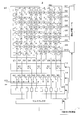
- FIG. 2 is a circuit diagram showing the configuration of the X-ray detector
- FIG. 3 is the periphery of the X-ray conversion layer of the X-ray detector.
- FIG. 4 is a block diagram showing the configuration of the amplifier array section.
- X-rays will be described as an example of incident light or radiation
- an X-ray imaging apparatus will be described as an example of light or radiation imaging apparatus.
- the X-ray imaging apparatus performs imaging by irradiating a subject with X-rays. Specifically, an X-ray image transmitted through the subject is projected on an X-ray conversion layer (in this embodiment, an amorphous selenium film), and carriers (charge signals) proportional to the density of the image are generated in the layer. Thus, it is converted into a charge signal.
- an X-ray conversion layer in this embodiment, an amorphous selenium film
- the X-ray imaging apparatus transmits an X-ray tube 1 that irradiates a subject M to be imaged with X-rays, a top plate 2 on which the subject M is placed, and the subject M.
- Generates a charge signal corresponding to the X-ray dose (detects X-rays as a charge signal), converts the charge signal into a voltage signal and outputs it, and outputs from the X-ray flat detector 3
- An A / D converter 4 for converting the converted voltage signal from analog to digital
- an image processing unit 5 for processing the digital voltage signal converted by the A / D converter 4 to form an image
- X-ray imaging A main control unit 6 that performs various controls on the X-ray tube, an X-ray tube control unit 7 that controls the X-ray tube 1 by generating a tube voltage and a tube current based on the control of the main control unit 6, and inputs related to X-ray imaging An X-ray image obtained by processing by the input unit 8 and the
- the X-ray flat panel detector 3 includes a plurality of X-ray detection elements DU, an X-ray detection control unit 11, a gate drive circuit 12, a first switching unit 13, a second switching unit 14, and an amplifier array unit. 15 and a multiplexer 16.
- the plurality of X-ray detection elements DU are connected to the gate drive circuit 12 through the gate lines G1 to G10, and are connected to the amplifier array unit 15 through the first switching unit 13 and the second switching unit 14 through the data lines D1 to D10.
- the X-ray detection control unit 11 is connected to the gate drive circuit 12, the first switching unit 13, the second switching unit 14, the amplifier array unit 15, and the multiplexer 16.
- the X-ray detection elements DU output charge signals in response to incident X-rays, and are arranged in a two-dimensional vertical and horizontal matrix on the X-ray detection surface SC on which X-rays are incident.
- X-ray detection elements DU are used, for example, arranged in a two-dimensional matrix in a length of about 4096 ⁇ width 4096.
- FIG. 2 an X-ray detection element DU arranged in a two-dimensional matrix of 10 ⁇ 10 is shown as an example.
- the X-ray detection surface SC corresponds to the light or radiation detection means in the present invention.
- the X-ray detection element DU includes a voltage application electrode 17 for applying a high bias voltage Va, an X-ray conversion layer 18 for converting incident X-rays into charge signals, and X-ray conversion. And an active matrix substrate 19 that collects, stores, and reads (outputs) the charge signals converted in the layer 18.
- the X-ray conversion layer 18 is made of an X-ray sensitive semiconductor, and is formed of, for example, an amorphous amorphous selenium (a-Se) film. Further, when X-rays enter the X-ray conversion layer 18, a predetermined number of carriers (charge signals) proportional to the energy of the X-rays are directly generated (direct conversion type).
- a-Se amorphous amorphous selenium
- the active matrix substrate 19 is provided with an insulating glass substrate 20, and an X-ray conversion is performed on the glass substrate 20 based on the application of the bias voltage Va to the voltage application electrode 17.
- the X-ray detection control unit 11 is controlled by the main control unit 6 (see FIG. 1). As shown in FIG. 2, the gate drive circuit 12, the first switching unit 13, the second switching unit 14, and the amplifier array unit 15 are used. And the multiplexer 16 are controlled in an integrated manner, and the charge signals detected by the X-ray detection element DU are selectively and sequentially taken out to the amplifier array unit 15 and further outputted from the multiplexer 16 in sequence.
- the X-ray detection control unit 11 includes a gate operation signal for starting the operation of the gate drive circuit 12, a first switching signal for turning on / off the switch S ⁇ b> 1 of the first switching unit 13, and the second switching unit 14.
- the second switching signal for turning ON / OFF the switches S2 and S3 the amplifier reset signal for starting the amplifier reset of the amplifier array unit 15, and the multiplexer control signal for controlling the operation of the multiplexer 16 are output. .
- the gate drive circuit 12 operates the TFT 22 of each X-ray detection element DU in order to selectively extract the charge signals detected by the X-ray detection element DU sequentially. Based on the gate operation signal from the X-ray detection control unit 11, the gate drive circuit 12 sequentially selects the gate lines G1 to G10 connected in common for each row of the X-ray detection elements DU and sends the gate signal. . At this time, as a method of selecting the gate lines G1 to G10, there are a normal mode for selecting one line at a time and a double mode for selecting two lines together.
- the TFTs 22 of the X-ray detection elements DU in the selected row are switched on simultaneously by the gate signal, and carriers (charge signals) accumulated in the capacitor Ca pass through the data lines D1 to D10 to the first switching unit 13. Is output.
- the gate drive circuit 12 corresponds to the switching signal operating means in the present invention, and the gate signal corresponds to the switching signal in the present invention.
- the first switching unit 13 connects the data lines D1 to D10 for each line via the switch S1. That is, as shown in FIG. 2, the data lines D1 and D2, D3 and D4, D5 and D6, D7 and D8, and D9 and D10 are connected via the switch S1, respectively.
- the switch S ⁇ b> 1 is controlled to be turned ON / OFF by the first switching signal from the X-ray detection control unit 11. In the normal mode, the switch S1 is always in the OFF state, and in the double mode, the switch S1 is always in the ON state.
- the first switching unit 13 corresponds to the first switching unit in the present invention.
- the second switching unit 14 connects the data lines D1 to D10 and the voltage signal detection unit 23 in the amplifier array unit 15 via switches S2 and S3.
- the switch S2 is connected to the data lines D1, D3, D5, D7, D9 whose data lines D1 to D10 are odd-numbered lines
- the switch S3 is the data line D2, D4 whose data lines D1 to D10 are even-numbered lines. , D6, D8, and D10.
- the switches S2 and S3 are in the ON state, the data lines D1 to D10 and the voltage signal detection unit 23 are connected and in a conductive state.
- the switch S2 and the switch S3 are in the OFF state, the ground line GR and the voltage signal detector 23 are connected.
- the switches S2 and S3 are ON / OFF controlled by the second switching signal from the X-ray detection control unit 11.
- the second switching unit 14 corresponds to the second switching unit in the present invention.
- the amplifier array section 15 is provided with a number (10 in FIG. 2) of voltage signal detection sections 23 corresponding to the data lines D1 to D10 for each column of the X-ray detection elements DU.
- the voltage signal detection unit 23 includes a charge detection amplifier circuit (CSA: Charge Sensitive Amplifier) 24, a low-pass filter 25, a signal amplifier circuit 26, and a sample hold circuit 27.
- CSA Charge Sensitive Amplifier
- the voltage signal detection unit 23 converts the charge signal read out through the data lines D1 to D10 into a voltage signal, and outputs a stable voltage signal to the multiplexer 16. Detailed explanation will be given later.
- the number of switches corresponding to the number of sample and hold circuits 27 is provided in the multiplexer 16. Further, the multiplexer 16 sequentially switches one of the switches to the ON state based on the multiplexer control signal from the X-ray detection control unit 11 and bundles the voltage signals output from the sample hold circuits 27 one by one. Is output to the A / D converter 4 as a time division signal.
- the A / D converter 4 samples each voltage signal of the time division signal from the multiplexer 16 at a predetermined timing, converts it to each voltage signal of a digital time division signal, and outputs it to the image processing unit 5. To do.
- the voltage signal detection unit 23 receives a charge signal output from each X-ray detection element DU and converts it into a voltage signal, and a voltage signal converted by the charge detection amplification circuit 24.
- a low-pass filter 25 that restricts the passage of high-frequency band component signals and a capacitor Cs1 that is a part of the low-pass filter 25, and a signal that amplifies the voltage signal that has passed through the low-pass filter 25 using the amplifying element A2.
- An amplifier circuit 26 and a sample hold circuit 27 that samples, holds and outputs the voltage signal amplified by the signal amplifier circuit 26 at a predetermined time are provided.
- the charge detection amplifier circuit 24 is an amplifying element, and an operational amplifier A1 whose inverting input terminal is connected to the data lines D1 to D10, and a feedback capacitor Cf1 provided between the inverting input terminal and the output terminal of the operational amplifier A1. And a switch SW1 provided in parallel with the feedback capacitor Cf1.
- a reference voltage Vref is applied to the non-inverting input terminal of the operational amplifier A1.
- the reference voltage Vref is a ground level (0 [V]).
- the charge detection amplification circuit 24 corresponds to charge voltage conversion means in the present invention.
- the switch SW1 changes to a conductive state (ON state) and a cut-off state (OFF state) based on the control from the X-ray detection control unit 11. Specifically, the switch SW1 is in a conductive state for a predetermined time based on the first amplifier reset signal from the X-ray detection control unit 11.
- the switch SW1 is in the conductive state, the charge accumulated in the feedback capacitor Cf1 is discharged, the feedback capacitor Cf1 is reset, and the charge detection amplifier circuit 24 is initialized.
- the switch SW1 is turned off after a predetermined time elapses, the initialization state is released, and the charge signals input from the data lines D1 to D10 after this time are accumulated in the feedback capacitor Cf1.
- the charge detection amplifier circuit 24 is configured to output a voltage signal corresponding to the charge signal input after the time point when the initialization state is released.
- the low-pass filter 25 includes a resistor R1 connected in series with the output terminal of the operational amplifier A1 of the charge detection amplifier circuit 24 and an input capacitor Cs1 connected in series with the resistor R1.
- the low-pass filter 25 is configured to output a voltage signal to the signal amplifier circuit 26 in a state where the passage of the high-frequency band component signal is restricted.
- the input capacitor Cs1 is a part of the configuration of the low-pass filter 25 and the signal amplifier circuit 26.
- the signal amplifying circuit 26 is one of the amplifying circuits.
- the operational amplifier A2 is an inverting amplifier for capacitor feedback, a feedback capacitor Cf2 provided between the inverting input terminal and the output terminal of the operational amplifier A2, and the feedback.
- a switch SW2 provided in parallel with the capacitor Cf2 and an input capacitor Cs1 having one end connected to the inverting input terminal of the operational amplifier A2 are provided.
- a reference voltage Vref is applied to the non-inverting input terminal of the operational amplifier A2.
- the signal amplifying circuit 26 corresponds to the voltage signal amplifying means in the present invention.
- the switch SW2 changes to a conductive state (ON state) and a cut-off state (OFF state) based on the control from the X-ray detection control unit 11. Specifically, the switch SW2 becomes conductive for a predetermined time based on the second amplifier reset signal from the X-ray detection control unit 11.
- the switch SW2 is in the conductive state, the charge accumulated in the feedback capacitor Cf2 is discharged, the feedback capacitor Cf2 is reset, and the signal amplifier circuit 26 is initialized.
- the signal amplifier circuit 26 including the input capacitor Cs1 and the feedback capacitor Cf2 is also a CDS (CorrelatedorSampling) circuit.
- the sample hold circuit 27 receives the voltage signal amplified by the signal amplifier circuit 26, samples the voltage signal at a predetermined time based on the sample hold control signal from the X-ray detection control unit 11, and outputs the voltage signal for a predetermined time. Is held (held), and a stable voltage signal is output to the multiplexer 16.
- the sample hold circuit 27 corresponds to the voltage signal holding means in the present invention.
- a charge detection amplifier circuit (CSA) 24 connected to the data lines D1, D3, D5, D7, D9, which are odd-numbered lines, via the switch S2, a signal amplifier circuit
- the (CDS) 26 and the sample hold circuit (S / H) 27 are a CSA odd channel, a CDS odd channel, and an S / H odd channel, respectively.
- the charge detection amplification circuit 24, the signal amplification circuit 26, and the sample hold circuit 27 connected to the data lines D2, D4, D6, D8, and D10 that are even-numbered lines via the switch S3 are respectively connected to the CSA even channel.
- FIG. 5 is a timing chart of the X-ray detection control unit according to the embodiment.
- the input unit 8 instructs to start X-ray imaging in the normal mode or the double mode.
- the gate line is selected for each line by the gate driving circuit 12 and the charge signal for each row is read out. It is most suitable for still image shooting with plenty of image processing time.
- the double mode is a pixel addition mode of 2 ⁇ 2 pixel addition.
- a charge detection signal of a total of four pixel regions, two in the row direction and two in the column direction, is added to obtain a radiation detection signal. Since the charge signal is read every two rows and the image processing time is shortened, it is optimal for moving image shooting.
- X-ray imaging in the double mode will be described.
- the main control unit 6 controls the X-ray tube control unit 7 and the X-ray detection control unit 11 of the X-ray flat panel detector 3 according to an instruction to start X-ray imaging from the input unit 8.
- the X-ray tube control unit 7 controls the X-ray tube 1 by generating tube voltage and tube current based on the control from the main control unit 6, and the subject M is irradiated with X-rays from the X-ray tube 1. Furthermore, the X-ray transmitted through the subject M is converted into a charge signal corresponding to the X-ray dose transmitted through the subject M by the X-ray detection element DU of the X-ray flat panel detector 3 and accumulated by the capacitor Ca.
- the X-ray detection control unit 11 sends a control signal for turning on the switch S1 of the first switching unit in the double mode based on the control from the main control unit 6.
- the switch S1 of the first switching unit 13 is turned on, so that the data lines D1 and D2, D3 and D4, D5 and D6, D7 and D8, and D9 and D10 are connected. In this way, charge signals are read simultaneously from two columns from the pixels connected to each data line.
- the X-ray detection control unit 11 also includes switches S2 and S3 of the second switching unit 14, a switch SW1 of the charge detection amplification circuit 24 in the voltage signal detection unit 23 in the amplifier array unit 15, and a switch SW2 of the signal amplification circuit 26. ON / OFF control and sample hold control of the sample hold circuit 27 are commanded.
- the X-ray detection control unit 11 outputs the first amplifier reset signal and the second amplifier reset signal to the CSA odd channel and the CDS odd channel connected to the switch S2 of the second switching unit 14.
- the switch SW1 of the CSA odd-numbered channel is turned on and the feedback capacitor Cf1 is reset, and the CSA odd-numbered channel is initialized as shown in FIG. 5C (t1 to t2).
- the switch S2 is in the OFF state.
- the CSA odd channel is connected to the ground line GR via the switch S2
- the CSA odd channel is initialized.
- the switch SW2 of the CDS odd channel is turned on by the second amplifier reset signal, the feedback capacitor Cf2 is reset, and the CDS odd channel is initialized (t1 to t4).
- the initialization of the CDS odd channel is performed even after the initialization of the CSA odd channel is completed. continuing.
- the switch S2 of the second switching unit 14 is turned on (t3).
- the CSA odd channel converts the charge signal read from the two connected data lines into a voltage signal.
- initialization of the CDS odd channel is continued.
- the input capacitor Cs1 of the CDS odd channel becomes a potential obtained by adding the potentials of the two data lines. That is, the input capacitor Cs1 changes from the ground level to a potential obtained by adding the potentials of the two connected data lines, and this is used as the base potential.
- the CDS odd channel starts to be initialized, and after the data line and the CSA odd channel are connected, the CDS odd channel is started. End initialization of.
- the X-ray detection control unit 11 outputs a gate operation signal to the gate drive circuit 12.
- the gate drive circuit 12 sequentially selects the gate lines every two lines. In this embodiment, description will be made assuming that two lines are selected in the order of the gate lines G1 and G2, G3 and G4,..., G9 and G10.
- the gate drive circuit 12 selects the gate lines G1 and G2, and each detection element DU connected to the gate lines G1 and G2 is designated.
- a voltage is applied to the gate of the TFT 22 of each designated detection element DU when a gate signal is sent from the gate drive circuit 12, and the gate is turned on (t4 to t6).
- carriers (charge signals) accumulated in the capacitor Ca connected to each designated TFT 22 are read to the data lines D1 to D10 via the TFT 22.
- the switches S2 and S3 of the second switching unit 14 are alternately turned on and off for each one-line readout period Ts.
- S2 is in the ON state (t3 to t8, t13 to t18)
- S3 is in the OFF state
- S2 is in the OFF state (t8 to t13, t18 to t23)
- S3 is in the ON state.
- the connected voltage signal detectors 23 are alternately switched every one line readout period Ts.
- the switch S1 of the first switching unit 13 is in the ON state, and the voltage signal detecting unit 23 to be connected is alternately switched every one line reading period Ts in the second switching unit 14, so that for each data line The read charge signal is added every two columns.
- the switch SW2 of the CDS odd channel is turned OFF to shut off.
- the voltage signal converted in the CSA odd channel is amplified in the CDS odd channel.
- the switches of the CSA even channel and the CDS even channel are ON, and initialization is started.
- the CSA even channel is initialized between t4 and t5, and the CDS even channel is initialized between t4 and t9.
- the CSA even channel is initialized when the CSA even channel is connected to the ground line GR via the switch S3, the CSA even channel is initialized.
- the CDS even channel starts to be initialized, and after the data line and the CSA even channel are connected, the CDS even channel is initialized. End conversion.
- the CSA even channel is turned off from t5 and accumulates a charge signal. However, since the switch S3 is connected to the ground line and no charge flows into the CSA even channel, the charge signal is not accumulated.
- CDS even channel is initializing while the CDS odd channel is accumulating voltage signals.
- CDS signal amplifier circuit
- the X-ray detection control unit 11 stops the gate operation signal to the gate drive circuit 12 (t6), and then sends a sample hold control signal to the S / H odd channel. With this signal, in the S / H odd channel, as shown in FIG. 5E, the potential of the difference between the potential of the voltage signal amplified in the CDS odd channel and the base potential is sampled (t7 to t8) and once. Hold.
- the X-ray detection control unit 11 sends a multiplexer control signal to the multiplexer 16 (t8).
- the voltage signal held in the odd-numbered S / H channel is output from the multiplexer 16 as a time division signal (t8 to t11).
- the output voltage signal is converted from an analog value to a digital value by the A / D converter 4.
- the image processing unit 5 Based on the converted digital signal, the image processing unit 5 performs signal processing to form a two-dimensional captured image.
- the gate drive circuit 12 selects the gate lines G3 and G4 (t9). Thereafter, in the same procedure, each detection element DU connected to the gate lines G3 and G4 is designated, and carriers (charge signals) accumulated in the capacitor Ca of each designated detection element DU are transferred to the data lines D1 to D1. Read to D10 (t9 to t11).
- the CSA odd channel and the CDS odd channel are initialized, and the CSA even channel and the CDS even channel respectively perform voltage conversion and voltage signal amplification in the same manner as described above. .
- the switches S2 and S3 of the second switching unit 14 are switched ON / OFF, whereby the charge detection amplification circuit 24 and the signal amplification circuit 26 can be initialized alternately.
- the charge signal and voltage signal added and accumulated via the two data lines can be initialized.
- the remaining gate lines G5 to G10 are similarly selected in order to read out charge signals in a two-dimensional manner.
- the gate driving circuit 12 sequentially selects the gate lines G1 to G10 line by line, so that the detection element DU connected to each gate line is designated, and the capacitor Ca of each designated detection element DU is applied to the capacitor Ca.
- the accumulated carriers (charge signals) are read out to the data lines D1 to D10.
- the charge signal converted by the X-ray detection element DU can be added and read via the data line.
- the charge detection amplification circuit 24 and the signal amplification circuit 26 in the voltage signal detection unit 23 not connected to the data line are initialized. be able to.
- the switching connection of the second switching unit 14 causes the operating voltage signal detection unit 23 and the charge detection amplification circuit 24 and the signal amplification circuit 26 in the voltage signal detection unit 23 to be initialized at the same time in parallel. Can be processed.
- the charge signal can be read out at high speed.
- the addition of the charge signal is not performed after the conversion to the voltage signal but before the conversion to the voltage signal, noise generated in the charge detection amplification circuit 24 is added to the voltage signal, and this is added to the signal amplification circuit 26. Will not amplify. As described above, since the charge signal is added before being input to the voltage signal detection unit 23, noise can be reduced as compared with the case where the voltage signal output from the voltage signal detection unit 23 is added.
- the present invention is not limited to the above embodiment, and can be modified as follows.
- the 2 ⁇ 2 pixel addition double mode is used.
- the three data lines are interposed between the three data lines.
- Two switches S1 may be connected to implement a triple mode of 3 ⁇ 3 pixel addition.
- the data lines D1 to D3, D4 to D6, and D7 to D9 are connected to each other, and charge signals for three pixels can be added in the row direction of the two-dimensional matrix. If gate signals are sent simultaneously from the gate drive circuit 12 to the gate lines G1 to G3, the charge signals for three pixels can be added in the column direction of the two-dimensional matrix.
- the gate lines G4 to G9 may also be sent in order by grouping three gate lines in order.
- the normal mode, the double mode, or the triple mode may be selected and implemented by connecting or disconnecting all the data lines with the switch S1.
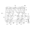
- the data line is connected by the first switching unit 13 so that the initialization of the voltage signal detection unit 23 can be alternately performed every time the gate line is selected. Therefore, as shown in FIG. 7, two voltage signal detectors 23 may be provided for each data line. That is, in the first switching unit 41, one of the two connection lines 42 is connected to one data line by the switch S4. In the second switching unit 43, The switch S5 switches the connection line 42 to the charge signal detection unit 23 and the connection between the ground line GR and the charge signal detection unit 23.
- the charge signal from the X-ray detection element DU is alternated. Can be read.
- the charge detection amplification circuit 24 and the signal amplification circuit 26 connected to the data line need only operate, the charge detection amplification circuit 24 and the signal amplification circuit 26 not connected to the data line are initialized. Can do.
- the charge detection amplification circuit 24 and the signal amplification circuit 26 which are operating, the charge detection amplification circuit 24 and the signal amplification circuit 26 to be initialized, Can be processed simultaneously in parallel.
- the charge signal can be read out at high speed.
- the voltage signal detectors 23 can be initialized alternately, so that image processing with higher image quality can be performed.
- the detection element DU is an X-ray sensitive semiconductor that is sensitive to X-rays.
- an optical imaging device that can perform high-speed readout with the same configuration. Can be produced.
Landscapes
- Engineering & Computer Science (AREA)
- Multimedia (AREA)
- Signal Processing (AREA)
- Transforming Light Signals Into Electric Signals (AREA)
- Apparatus For Radiation Diagnosis (AREA)
- Measurement Of Radiation (AREA)
Abstract
本発明の放射線撮像装置に備わるX線平面検出器3には、電荷信号を読み出すデータ線同士を接続または遮断する第1切り替え部13を備えることで、画素加算モードと通常の撮像モードとを選択してX線撮像を行うことができる。また、さらにデータ線と電圧信号検出部23との間に第2切り替え部14を備えることで、ゲート線を選択する度に、電圧信号検出部23内の電荷検出増幅回路24および信号増幅回路26の初期化を交互に行うことができる。この結果、電荷検出増幅回路24および信号増幅回路26を十分に初期化することができつつ、X線検出信号を高速に読み出すことができる。
Description
本発明は、医療分野や非破壊検査、RI(Radio Isotope)検査、および光学検査などの産業分野などに用いられる光または放射線撮像装置に係り、特に、光または放射線を検出する検出素子からの電荷信号を読み出す回路を備えた光または放射線撮像装置に関する。
従来、光または放射線撮像装置には、光または放射線を検出する光または放射線検出器を備えている。ここで光とは、赤外線、可視光線、紫外線、放射線、γ線等をいうが、特にX線検出器を例に採って説明する。X線検出器にはX線感応型のX線変換層を備えており、X線の入射によりX線変換層はキャリア(電荷信号)を生成し、その生成された電荷信号を読み出すことでX線を検出する。
被検体にX線を照射してX線撮像を行う場合には、被検体を透過したX線強度の強弱に比例したキャリア(電荷信号)がX線変換層内に発生する。その後、X線変換層内で生成されたキャリア(電荷信号)が、2次元状に配列されたキャリア収集電極に収集されて、所定時間分だけ蓄積された後、薄膜トランジスタ(TFT)を介してデータ線を通じて外部に読み出される。また、このようなX線検出器を製造するには、2次元状に配列された薄膜トランジスタ(TFT)からなるスイッチング素子や上述したキャリア収集電極などをパターン形成した絶縁基板上に、X線変換型の半導体膜を蒸着することで得られる。
さらに、X線検出器は、例えば、X線変換層で生成された電荷信号を電圧信号に変換する電荷検出増幅回路(CSA)と、電荷検出増幅回路からの電圧信号を増幅する信号増幅回路と、信号増幅回路から出力される電圧信号をサンプリングし、このサンプリングされた電圧信号を保持(ホールド)し、出力するサンプルホールド回路とを備えたものがある(例えば、特許文献1参照)。また、サンプルホールド回路から出力された電圧信号をマルチプレクサにより時分割し、さらに、この時分割された電圧信号をA/D変換器でデジタル信号に変換している。
特開2007-306481号公報
しかしながら、特許文献1に開示されている方法では、各データ線の読み出し動作は、電荷検出増幅回路および信号増幅回路のクリア、電荷蓄積、電圧ホールドという手順になるが、ゲート線1ラインの読み出し時間に対して、この電荷検出増幅回路および信号増幅回路のクリア時間の占める割合が大きくなる問題が発生した。さらには、放射線検出器の画素数が多くなればなるほど、ゲート線のライン数が増加するので、1ラインの読み出し時間が短くなることも原因である。このような理由により、高速な電圧信号の読み出しに限界が生じ、特に大画面になる程、動画での放射線透過画像の作成は困難であった。
本発明は、このような事情に鑑みてなされたものであって、光または放射線変換層で生成された電荷信号を電圧信号へ変換する一連の読み込みを高速ですることができる光または放射線撮像装置を提供することを目的とする。
本発明は、このような目的を達成するために、次のような構成をとる。
すなわち、本発明の第1の発明は、光または放射線撮像装置であって、光または放射線に感応して電荷信号を生成する検出素子が2次元マトリックス状に複数個配設された光または放射線検出手段と、前記光または放射線検出手段の2次元マトリックスの行ごとに前記電荷信号を読み出すスイッチング信号を送るスイッチング信号稼働手段と、前記光または放射線検出手段からデータ線を介して読み出される電荷信号を電圧信号に変換する電荷電圧変換手段と、前記電荷電圧変換手段にて変換された電圧信号を増幅する電圧信号増幅手段と、前記電圧信号増幅手段にて増幅された電圧信号を一定時間サンプリングして所定の時間保持する電圧信号保持手段と、前記データ線間を接続または遮断する第1切り替え手段と、前記データ線と前記電荷電圧変換手段との接続、または、接地ラインと前記電荷電圧変換手段との接続のいずれかに切り替え接続をする第2切り替え手段とを備え、前記第1切り替え手段により前記データ線間が接続されることで、複数のデータ線上に接続された検出素子からの電荷信号を同時に読み出すことができることを特徴とする。
すなわち、本発明の第1の発明は、光または放射線撮像装置であって、光または放射線に感応して電荷信号を生成する検出素子が2次元マトリックス状に複数個配設された光または放射線検出手段と、前記光または放射線検出手段の2次元マトリックスの行ごとに前記電荷信号を読み出すスイッチング信号を送るスイッチング信号稼働手段と、前記光または放射線検出手段からデータ線を介して読み出される電荷信号を電圧信号に変換する電荷電圧変換手段と、前記電荷電圧変換手段にて変換された電圧信号を増幅する電圧信号増幅手段と、前記電圧信号増幅手段にて増幅された電圧信号を一定時間サンプリングして所定の時間保持する電圧信号保持手段と、前記データ線間を接続または遮断する第1切り替え手段と、前記データ線と前記電荷電圧変換手段との接続、または、接地ラインと前記電荷電圧変換手段との接続のいずれかに切り替え接続をする第2切り替え手段とを備え、前記第1切り替え手段により前記データ線間が接続されることで、複数のデータ線上に接続された検出素子からの電荷信号を同時に読み出すことができることを特徴とする。
本発明の第1の発明によれば、データ線間を接続または遮断する第1切り替え手段と、データ線と電荷電圧変換手段との接続、および接地ラインと電荷電圧変換手段との接続のいずれかに切り替え接続をする第2切り替え手段とを備えるので、検出素子からの電荷信号を複数のデータ線を介して加算して読み込むことができる。また、データ線と接続されている電荷電圧変換手段と電圧信号増幅手段が動作すればよいので、データ線と接続されていない電荷電圧変換手段と電圧信号増幅手段とを初期化することができる。このように、第2切り替え手段の切り替え接続により、動作している電荷電圧変換手段および電圧信号増幅手段と、初期化する電荷電圧変換手段および電圧信号増幅手段とを同時に並行して処理することができる。これより、電荷信号を高速に読み出すことができる光または放射線撮像装置が得られる。
また、第2切り替え手段により、接地ラインと前記電荷電圧変換手段とが接続されているときに、前記電荷電圧変換手段の電荷信号を消去すればよい。これより、電荷電圧変換手段の電荷信号を確実に消去して初期化することができる。
また、第2切り替え手段により、接地ラインと前記電荷電圧変換手段とが接続されているときに、前記電圧信号増幅手段の初期化を開始するとともに、第2切り替え手段により、前記データ線と前記電荷電圧変換手段とが接続された後に、前記電圧信号増幅手段の初期化を終了すればよい。これより、電圧信号増幅手段の初期化を確実に行うことができ、また、電圧信号増幅手段の初期化をデータ線と電荷電圧変換手段とが接続された後に初期化を終了することで、電圧信号増幅手段のベース電位をデータ線の電位に合わすことができる。
また、第1切り替え手段は、前記データ線を2ラインずつ接続または遮断してもよい。 これより、光または放射線検出器の2次元マトリックスの行方向の2画素の電荷信号を加算することができる。これより、電荷信号を高速に読み出すことができる。
本発明の第2の発明は、光または放射線撮像装置であって、光または放射線に感応して電荷信号を生成する検出素子が2次元マトリックス状に複数個配設された光または放射線検出手段と、前記光または放射線検出手段の2次元マトリックスの行ごとに前記電荷信号を読み出すスイッチング信号を送るスイッチング信号稼働手段と、前記光または放射線検出手段からデータ線を介して読み出される電荷信号を電圧信号に変換する電荷電圧変換手段と、前記電荷電圧変換手段にて変換された電圧信号を増幅する電圧信号増幅手段と、前記電圧信号増幅手段にて増幅された電圧信号を一定時間サンプリングして所定の時間保持する電圧信号保持手段と、前記データ線をそれぞれ2本の接続ラインのいずれかと接続または遮断する第1切り替え手段と、前記接続ラインと前記電荷電圧変換手段との接続、または、接地ラインと前記電荷電圧変換手段との接続のいずれかに切り替え接続をする第2切り替え手段と、1本の前記データ線に対して、前記電荷電圧変換手段および前記電圧信号増幅手段並びに前記電圧信号保持手段とを並列に2組備えたことを特徴とする。
本発明の第2の発明によれば、1本のデータ線に対して2本の接続ラインのいずれかと接続または遮断する第1切り替え手段と、接続ラインと電荷電圧変換手段との接続、および接地ラインと電荷電圧変換手段との接続のいずれかに切り替え接続をする第2切り替え手段と、1本のデータ線に対して、電荷電圧変換手段および電圧信号増幅手段並びに電圧信号保持手段とを並列に2組備えるので、検出素子からの電荷信号を交互に読み込むことができる。また、データ線と接続されている電荷電圧変換手段と電圧信号増幅手段が動作すればよいので、データ線と接続されていない電荷電圧変換手段と電圧信号増幅手段を初期化することができる。このように、第1切り替え手段および第2切り替え手段の切り替え接続により、動作している電荷電圧変換手段および電圧信号増幅手段と、初期化する電荷電圧変換手段および電圧信号増幅手段とを同時に並行して処理することができる。これより、電荷信号を高速に読み出すことができる光または放射線撮像装置が得られる。
本発明に係る放射線または光撮像装置によれば、データ線と接続されている電荷電圧変換手段と電圧信号増幅手段が動作すればよいので、データ線と接続されていない電荷電圧変換手段と電圧信号増幅手段とを初期化することができる。このように、第2切り替え手段の切り替え接続により、動作している電荷電圧変換手段および電圧信号増幅手段と、初期化する電荷電圧変換手段および電圧信号増幅手段とを同時に並行して処理することができる。これより、光または放射線検出手段で生成された電荷信号を電圧信号へ変換する一連の読み込みを高速ですることができる。
1 … X線管
3 … X線平面検出器
4 … A/D変換器
5 … 画像処理部
11 … X線検出制御部
12 … ゲート駆動回路
13 … 第1切り替え部
14 … 第2切り替え部
15 … アンプアレイ部
16 … マルチプレクサ
23 … 電圧信号検出部
24 … 電荷検出増幅回路
25 … ローパスフィルタ
26 … 信号増幅回路
27 … サンプルホールド回路
DU … 検出素子
SC … 検出面
G1~G10 … ゲート線
D1~D10 … データ線
3 … X線平面検出器
4 … A/D変換器
5 … 画像処理部
11 … X線検出制御部
12 … ゲート駆動回路
13 … 第1切り替え部
14 … 第2切り替え部
15 … アンプアレイ部
16 … マルチプレクサ
23 … 電圧信号検出部
24 … 電荷検出増幅回路
25 … ローパスフィルタ
26 … 信号増幅回路
27 … サンプルホールド回路
DU … 検出素子
SC … 検出面
G1~G10 … ゲート線
D1~D10 … データ線
以下、図面を参照して本発明の実施例を説明する。
図1は実施例に係るX線撮像装置の構成を示すブロック図であり、図2はX線検出器の構成を示す回路図であり、図3はX線検出器のX線変換層周辺部の概略断面図であり、図4はアンプアレイ部の構成を示すブロック図である。本実施例では、入射する光または放射線としてX線を例に採って説明するとともに、光りまたは放射線撮像装置としてX線撮像装置を例に採って説明する。
図1は実施例に係るX線撮像装置の構成を示すブロック図であり、図2はX線検出器の構成を示す回路図であり、図3はX線検出器のX線変換層周辺部の概略断面図であり、図4はアンプアレイ部の構成を示すブロック図である。本実施例では、入射する光または放射線としてX線を例に採って説明するとともに、光りまたは放射線撮像装置としてX線撮像装置を例に採って説明する。
<X線撮像装置>
本実施例に係るX線撮像装置は、被検体にX線を照射して撮像を行う。具体的には、被検体を透過したX線像がX線変換層(本実施例ではアモルファスセレン膜)上に投影されて、像の濃淡に比例したキャリア(電荷信号)が層内に発生することで電荷信号に変換される。
本実施例に係るX線撮像装置は、被検体にX線を照射して撮像を行う。具体的には、被検体を透過したX線像がX線変換層(本実施例ではアモルファスセレン膜)上に投影されて、像の濃淡に比例したキャリア(電荷信号)が層内に発生することで電荷信号に変換される。
図1に示すように、X線撮像装置は、撮像対象である被検体MにX線を照射するX線管1と、被検体Mを載置させる天板2と、被検体Mを透過したX線量に応じた電荷信号を生成(X線を電荷信号として検出)し、さらに、この電荷信号を電圧信号に変換して出力するX線平面検出器3と、X線平面検出器3から出力された電圧信号をアナログからデジタルへ変換するA/D変換器4と、A/D変換器4で変換されたデジタルの電圧信号を処理して画像を構成する画像処理部5と、X線撮像に関する種々の制御を行う主制御部6と、主制御部6での制御に基づいて管電圧や管電流を発生させX線管1を制御するX線管制御部7と、X線撮像に関する入力設定を行うことが可能な入力部8、画像処理部5で処理されて得られたX線画像などを表示する表示部9、画像処理部5で処理されて得られたX線画像などを記憶する記憶部10などを備えている。さらに、X線撮像装置の各部構成を詳細に説明する。
図2に示すように、X線平面検出器3は、複数のX線検出素子DU、X線検出制御部11、ゲート駆動回路12、第1切り替え部13、第2切り替え部14、アンプアレイ部15、マルチプレクサ16とが備えられている。これら複数のX線検出素子DUは、ゲート線G1~G10によりゲート駆動回路12と接続し、データ線D1~D10により第1切り替え部13および第2切り替え部14を介してアンプアレイ部15と接続されている。X線検出制御部11は、ゲート駆動回路12、第1切り替え部13、第2切り替え部14、アンプアレイ部15、およびマルチプレクサ16とに接続されている。
X線検出素子DUは、入射されたX線に感応して電荷信号を出力するものであり、X線が入射されるX線検出面SCに縦横の2次元マトリックス状に配列されている。実際のX線検出面SCにはX線検出素子DUが、例えば、縦4096×横4096程度に2次元マトリックス状に配列されて用いられる。なお、図2においては、X線検出素子DUが縦10×横10の2次元マトリックス状に配列したものを一例として図示している。X線検出面SCは本発明における光または放射線検出手段に相当する。
また、X線検出素子DUは図3に示されるように、高電圧のバイアス電圧Vaを印加する電圧印加電極17と、入射したX線から電荷信号へ変換するX線変換層18とX線変換層18で変換された電荷信号を収集、蓄積、読み出し(出力)を行うアクティブマトリックス基板19とを備えている。
X線変換層18は、X線感応型半導体からなり、例えば、非晶質のアモルファスセレン(a-Se)膜で形成されている。また、X線変換層18にX線が入射すると、このX線のエネルギーに比例した所定個数のキャリア(電荷信号)が直接生成される構成(直接変換型)となっている。
アクティブマトリックス基板19は図3に示すように、絶縁性のガラス基板20が設けられ、このガラス基板20上には、電圧印加電極17にバイアス電圧Vaが印加されたことに基づいて、X線変換層18で変換された電荷信号を収集する収集電極21、収集電極21で収集された電荷信号を蓄積するコンデンサCa、スイッチング素子としてのTFT22、ゲート駆動回路12からTFT22を制御するためのゲート線G1~G10、TFT22から電荷信号が読み出されるデータ線D1~D10とを設けている。
次に、X線検出制御部11は主制御部6(図1参照)から制御され、図2に示すようにゲート駆動回路12と第1切り替え部13と第2切り替え部14とアンプアレイ部15とマルチプレクサ16とを統括制御するものであり、X線検出素子DUで検出された電荷信号を順次選択的にアンプアレイ部15へ取り出し、さらに、マルチプレクサ16から順次出力させる制御を行うものである。具体的にはX線検出制御部11は、ゲート駆動回路12の動作を開始させるゲート動作信号と、第1切り替え部13のスイッチS1をON・OFFさせる第1切り替え信号と、第2切り替え部14のスイッチS2およびスイッチS3をON・OFFさせる第2切り替え信号と、アンプアレイ部15のアンプリセットを開始させるアンプリセット信号と、マルチプレクサ16の動作を制御するマルチプレクサ制御信号を出力する構成となっている。
次に、ゲート駆動回路12は、X線検出素子DUで検出された電荷信号を順次選択的に取り出すために、各X線検出素子DUのTFT22を動作させるものである。ゲート駆動回路12は、X線検出制御部11からのゲート動作信号に基づいて、X線検出素子DUの横行ごとに共通して接続されるゲート線G1~G10を順次選択してゲート信号を送る。このとき、ゲート線G1~G10の選択の方法として、1ラインずつ選択するノーマルモードと2ラインまとめて選択するダブルモードとがある。この選択した行内のX線検出素子DUのTFT22は、ゲート信号により一斉にスイッチオン状態になり、コンデンサCaに蓄積されたキャリア(電荷信号)がデータ線D1~D10を通り第1切り替え部13に出力される。ゲート駆動回路12は、本発明におけるスイッチング信号稼働手段に相当し、ゲート信号は、本発明におけるスイッチング信号に相当する。
次に、第1切り替え部13は、データ線D1~D10を1ラインごとにスイッチS1を介して接続する。すなわち、図2に示すように、データ線D1とD2、D3とD4、D5とD6、D7とD8、D9とD10がそれぞれスイッチS1を介して接続されている。X線検出制御部11からの第1切り替え信号により、スイッチS1はON・OFFの制御がされる。ノーマルモードでは、スイッチS1は常にOFF状態であり、ダブルモードではスイッチS1は常にON状態である。第1切り替え部13は本発明における第1切り替え手段に相当する。
次に、第2切り替え部14は、データ線D1~D10とアンプアレイ部15内の電圧信号検出部23との間にスイッチS2およびS3を介して接続する。スイッチS2はデータ線D1~D10が奇数番目のラインであるデータ線D1、D3、D5、D7、D9と接続され、スイッチS3はデータ線D1~D10が偶数番目のラインであるデータ線D2、D4、D6、D8、D10と接続されている。スイッチS2およびスイッチS3がON状態のときに、データ線D1~D10と電圧信号検出部23とが接続され導通状態にある。スイッチS2およびスイッチS3がOFF状態の時には、接地ラインGRと電圧信号検出部23とが接続される。スイッチS2およびスイッチS3は、X線検出制御部11からの第2切り替え信号により、ON・OFFの制御がされる。第2切り替え部14は本発明における第2切り替え手段に相当する。
次に、アンプアレイ部15は、X線検出素子DUの縦列ごとのデータ線D1~D10に対応した数(図2では10個)の電圧信号検出部23が備えられている。電圧信号検出部23は、電荷検出増幅回路(CSA:Charge Sensitive Amplifier)24とローパスフィルタ25と信号増幅回路26とサンプルホールド回路27とが備えられている。電圧信号検出部23では、データ線D1~D10を介して読み出された電荷信号を電圧信号に変換し、安定した状態の電圧信号をマルチプレクサ16に出力する。詳細な説明は後で行う。
次に、マルチプレクサ16の内部には、サンプルホールド回路27の数に対応した数のスイッチが設けられている。また、マルチプレクサ16は、X線検出制御部11からのマルチプレクサ制御信号に基づいてスイッチのいずれかひとつを順次ON状態に切り替えて、各サンプルホールド回路27から出力される電圧信号の一つずつを束ねた時分割信号としてA/D変換器4へ出力する。
次に、A/D変換器4は、マルチプレクサ16からの時分割信号の各電圧信号について、所定のタイミングでサンプリングしてデジタルの時分割信号の各電圧信号に変換し、画像処理部5へ出力する。
<電圧信号検出部>
以下に、電圧信号検出部23の電気的構成を図4を用いて詳細に説明する。
電圧信号検出部23は、各X線検出素子DUから出力された電荷信号を入力し、電圧信号に変換する電荷検出増幅回路(CSA)24と、この電荷検出増幅回路24で変換された電圧信号において、高周波帯域成分の信号の通過を制限するローパスフィルタ25と、ローパスフィルタ25の一部であるコンデンサCs1と結合し、ローパスフィルタ25を通過した電圧信号を、増幅素子A2を用いて増幅する信号増幅回路26と、信号増幅回路26で増幅された電圧信号をサンプリングし所定の時間において保持し、出力するサンプルホールド回路27とを備えている。
以下に、電圧信号検出部23の電気的構成を図4を用いて詳細に説明する。
電圧信号検出部23は、各X線検出素子DUから出力された電荷信号を入力し、電圧信号に変換する電荷検出増幅回路(CSA)24と、この電荷検出増幅回路24で変換された電圧信号において、高周波帯域成分の信号の通過を制限するローパスフィルタ25と、ローパスフィルタ25の一部であるコンデンサCs1と結合し、ローパスフィルタ25を通過した電圧信号を、増幅素子A2を用いて増幅する信号増幅回路26と、信号増幅回路26で増幅された電圧信号をサンプリングし所定の時間において保持し、出力するサンプルホールド回路27とを備えている。
電荷検出増幅回路24は、増幅素子であり、反転入力端子がデータ線D1~D10に接続された演算増幅器A1と、この演算増幅器A1の反転入力端子および出力端子の間に設けられた帰還コンデンサCf1と、この帰還コンデンサCf1に並列に設けられたスイッチSW1とを備えている。また、演算増幅器A1の非反転入力端子には、基準電圧Vrefが印加されている。なお、基準電圧Vrefは、接地レベル(0[V])である。電荷検出増幅回路24は本発明における電荷電圧変換手段に相当する。
また、スイッチSW1は、X線検出制御部11からの制御に基づいて、導通状態(ON状態)および遮断状態(OFF状態)に変化するものである。具体的には、スイッチSW1はX線検出制御部11からの第1アンプリセット信号に基づいて、所定の時間において導通状態となる。ここで、スイッチSW1が導通状態の場合には、帰還コンデンサCf1に蓄積された電荷が放電され、帰還コンデンサCf1がリセットされた状態となり、電荷検出増幅回路24が初期化された状態となる。さらに、所定の時間経過後にスイッチSW1が遮断状態になると初期化状態が解除され、この時点以降にデータ線D1~D10から入力された電荷信号が帰還コンデンサCf1に蓄積される。これより、電荷検出増幅回路24は、初期化状態が解除された時点以降に入力された電荷信号に応じた電圧信号を出力する構成である。
ローパスフィルタ25は、電荷検出増幅回路24の演算増幅器A1の出力端と直列に接続された抵抗R1と、この抵抗R1に直列に接続された入力コンデンサCs1により構成される。このローパスフィルタ25により、高周波帯域成分の信号の通過を制限した状態で電圧信号を信号増幅回路26に出力する構成である。なお、入力コンデンサCs1は、ローパスフィルタ25および信号増幅回路26の構成の一部である。
信号増幅回路26は、増幅回路の一つであり、コンデンサ帰還の反転増幅器である演算増幅器A2と、この演算増幅器A2の反転入力端子および出力端子の間に設けられた帰還コンデンサCf2と、この帰還コンデンサCf2に並列に設けられたスイッチSW2と、演算増幅器A2の反転入力端子に一端が接続された入力コンデンサCs1とを備えている。また、演算増幅器A2の非反転入力端子には、基準電圧Vrefが印加されている。信号増幅回路26は、本発明における電圧信号増幅手段に相当する。
また、スイッチSW2は、X線検出制御部11からの制御に基づいて、導通状態(ON状態)および遮断状態(OFF状態)に変化するものである。具体的には、スイッチSW2はX線検出制御部11からの第2アンプリセット信号に基づいて、所定の時間において導通状態となる。ここで、スイッチSW2が導通状態の場合には、帰還コンデンサCf2に蓄積された電荷が放電され、帰還コンデンサCf2がリセットされた状態となり、信号増幅回路26が初期化された初期化状態となる。さらに、所定の時間経過後にスイッチSW2が遮断状態になると、信号増幅回路26は、倍率MA=|Cs1/Cf2|で、入力された電圧信号を反転増幅して出力する増幅状態となる。また、入力コンデンサCs1と帰還コンデンサCf2を備える信号増幅回路26はCDS(Correlated Double Sampling)回路でもある。
サンプルホールド回路27は、信号増幅回路26で増幅された電圧信号を入力し、X線検出制御部11からのサンプルホールド制御信号に基づいて、この電圧信号を所定の時間においてサンプリングし、所定の時間が経過した時点での電圧信号を保持(ホールド)し、安定した状態の電圧信号をマルチプレクサ16に出力する。サンプルホールド回路27は、本発明における電圧信号保持手段に相当する。
また、スイッチS1のON・OFFに関係なく、スイッチS2を介して奇数番目のラインであるデータ線D1、D3、D5、D7、D9と接続される電荷検出増幅回路(CSA)24、信号増幅回路(CDS)26、サンプルホールド回路(S/H)27をそれぞれ、CSA奇数チャンネル、CDS奇数チャンネル、S/H奇数チャンネルとする。同様に、スイッチS3を介して偶数番目のラインであるデータ線D2、D4、D6、D8、D10と接続される電荷検出増幅回路24、信号増幅回路26、サンプルホールド回路27をそれぞれ、CSA偶数チャンネル、CDS偶数チャンネル、S/H偶数チャンネルとする。
<X線撮像>
次に、本実施例におけるX線撮像装置でX線撮像が実行される場合の動作を、図1~図5を用いて説明する。図5は、実施例に係るX線検出制御部のタイミングチャート図である。
次に、本実施例におけるX線撮像装置でX線撮像が実行される場合の動作を、図1~図5を用いて説明する。図5は、実施例に係るX線検出制御部のタイミングチャート図である。
まず、入力部8においてノーマルモードかダブルモードかでのX線撮像開始の指示をする。ノーマルモードにおいては、ゲート駆動回路12よりゲート線が1ラインごとに選択されて、各行ごとの電荷信号を読み出す。画像処理時間に余裕のある静止画撮影時に最適である。
これに対して、ダブルモードとは、2×2画素加算の画素加算モードである。行方向に2個と列方向に2個の合計4個の画素領域の電荷信号を加算して放射線検出信号を得る。2行ごとに電荷信号を読み取り、画像処理時間の短縮化になるので、動画撮影時に最適である。以下、ダブルモードでのX線撮像の説明をする。
入力部8からのX線撮像開始の指示により、主制御部6は、X線管制御部7とX線平面検出器3のX線検出制御部11とを制御する。X線管制御部7は、主制御部6からの制御に基づいて管電圧や管電流を発生させX線管1を制御し、X線管1からX線が被検体Mに照射される。さらに、被検体Mを透過したX線は、X線平面検出器3のX線検出素子DUにより被検体Mを透過したX線量に応じた電荷信号に変換され、コンデンサCaにより蓄積される。
次に、図5を用いて、各検出素子DUにゲート線G1~G10を介して接続されたゲート駆動回路12の動作、およびデータ線D1~D10を介して接続された第1切り替え部13、第2切り替え部14、アンプアレイ部15の動作、並びにこれらを制御するX線検出制御部11の動作を説明する。
X線検出制御部11は、主制御部6からの制御に基づいて、ダブルモード時には第1切り替え部のスイッチS1をONにする制御信号を送る。これにより、第1切り替え部13のスイッチS1が導通するので、データ線D1とD2、D3とD4、D5とD6、D7とD8、D9とD10とがそれぞれ接続される。このようにして、各データ線に接続された画素から2列同時に電荷信号を読み込む。
また、X線検出制御部11は、第2切り替え部14のスイッチS2およびS3とアンプアレイ部15内の電圧信号検出部23内の電荷検出増幅回路24のスイッチSW1および信号増幅回路26のスイッチSW2のON・OFF制御およびサンプルホールド回路27のサンプルホールド制御を指令する。
まず、X線検出制御部11は、第2切り替え部14のスイッチS2と接続されるCSA奇数チャンネルと、CDS奇数チャンネルに対して、第1アンプリセット信号および第2アンプリセット信号を出力する。この第1アンプリセット信号により、CSA奇数チャンネルのスイッチSW1がON状態で導通し、帰還コンデンサCf1がリセットされ、図5(c)に示すように、CSA奇数チャンネルが初期化する(t1~t2)。この時、図5(b)に示すように、スイッチS2はOFF状態である。このように、CSA奇数チャンネルがスイッチS2を介して接地ラインGRと接続しているときに、CSA奇数チャンネルが初期化する。また、第2アンプリセット信号により、CDS奇数チャンネルのスイッチSW2がON状態で導通し、帰還コンデンサCf2がリセットされ、CDS奇数チャンネルが初期化する(t1~t4)。この際、電荷検出増幅回路(CSA)24よりも信号増幅回路(CDS)26を初期化する方が時間を要するので、CSA奇数チャンネルの初期化が終わった後でも、CDS奇数チャンネルの初期化を継続している。
次に、第2切り替え部14のスイッチS2がON状態(t3)になる。この際、CSA奇数チャンネルは、接続された2本のデータ線から読み出される電荷信号を電圧信号へと変換する。しかしながら、この時点では、CDS奇数チャンネルの初期化を継続している。これより、CDS奇数チャンネルの入力コンデンサCs1は、2本のデータ線のそれぞれの電位を加算した電位となる。つまり、入力コンデンサCs1は、接地準位から、接続された2本のデータ線のそれぞれの電位を加算した電位へと変化し、これをベース電位とする。このように、CSA奇数チャンネルがスイッチS2を介して接地ラインGRと接続されているときにCDS奇数チャンネルも初期化を開始して、データ線とCSA奇数チャンネルとが接続された後に、CDS奇数チャンネルの初期化を終了する。
次に、X線検出制御部11はゲート駆動回路12に対してゲート動作信号を出力する。このゲート動作信号により、図5(a)に示すように、ゲート駆動回路12がゲート線を2ライン毎に順次選択する。本実施例では、ゲート線G1およびG2,G3およびG4,…,G9およびG10の順に2ラインずつ選択するものとして説明する。
先ず、ゲート駆動回路12がゲート線G1およびG2を選択して、ゲート線G1およびG2に接続された各検出素子DUが指定される。指定された各検出素子DUのTFT22のゲートは、ゲート駆動回路12からゲート信号が送られることで電圧が印加され、ON状態(t4~t6)となる。これより、指定された各TFT22に接続されるコンデンサCaに蓄積されたキャリア(電荷信号)が、TFT22を経由して、データ線D1~D10に読み出される。
また、図5(b)と(f)に示すように、1ライン読み出し期間Tsごとに、第2切り替え部14のスイッチS2およびS3は交互にON・OFF状態になっている。S2がON状態である時(t3~t8、t13~t18)は、S3はOFF状態であり、S2がOFF状態である時(t8~t13、t18~t23)は、S3はON状態である。これより、1ライン読み出し期間Tsごとに、接続される電圧信号検出部23が交互に入れ替わる。
さらに、第1切り替え部13のスイッチS1がON状態にあり、第2切り替え部14にて1ライン読み出し期間Tsごとに、接続される電圧信号検出部23が交互に入れ替わるので、各データ線ごとに読み出された電荷信号は、2列ごとに加算される。
そして、CDS奇数チャンネルがベース電位へ移行した時点(t4)で、CDS奇数チャンネルのスイッチSW2をOFFして、遮断する。これにより、CSA奇数チャンネルで変換された電圧信号がCDS奇数チャンネルにて増幅される。
この時(t4)、CSA偶数チャネルおよび、CDS偶数チャンネルはスイッチがON状態であり、初期化を開始する。CSA偶数チャネルについてはt4~t5の間、CDS偶数チャンネルについてはt4~t9の間初期化する。このように、CSA偶数チャンネルがスイッチS3を介して接地ラインGRと接続しているときに、CSA偶数チャンネルが初期化する。また、CSA偶数チャンネルがスイッチS3を介して接地ラインGRと接続されているときにCDS偶数チャンネルも初期化を開始して、データ線とCSA偶数チャンネルとが接続された後に、CDS偶数チャンネルの初期化を終了する。CSA偶数チャネルはt5からOFF状態になり電荷信号を蓄積する状態になるが、スイッチS3が接地ラインと接続されておりCSA偶数チャネルには電荷が流れ込まないので、電荷信号を蓄積することはない。
そして、CDS奇数チャンネルが電圧信号を蓄積している間に、CDS偶数チャンネルは初期化している。このように、交互に信号増幅回路(CDS)26を初期化することで、初期化するのに十分な時間を確保している。
そして、X線検出制御部11はゲート駆動回路12へゲート動作信号を停止した後(t6)、S/H奇数チャンネルへサンプルホールド制御信号を送る。この信号により、S/H奇数チャンネルでは、図5(e)に示すように、CDS奇数チャンネルで増幅された電圧信号の電位とベース電位との差の電位をサンプリングする(t7~t8)とともに一旦ホールドする。
その後、X線検出制御部11はマルチプレクサ16へマルチプレクサ制御信号を送る(t8)。この信号により、図5(j)に示すように、マルチプレクサ16からS/H奇数チャンネルにホールドされた電圧信号を時分割信号として出力する(t8~t11)。出力された電圧信号はA/D変換器4にてアナログ値からデジタル値へ変換される。この変換されたデジタル信号に基づいて、画像処理部5は信号処理を行って、2次元状の撮像画像を構成する。
次に、第2切り替え部14のスイッチS2がOFF状態に、スイッチS3がON状態になった(t8)後に、ゲート駆動回路12がゲート線G3およびG4を選択する(t9)。その後、同様の手順で、ゲート線G3およびG4に接続された各検出素子DUが指定され、その指定された各検出素子DUのコンデンサCaに蓄積されたキャリア(電荷信号)が、データ線D1~D10に読み出される(t9~t11)。
このように、次の1ライン読み出し期間Tsでは、CSA奇数チャンネルおよびCDS奇数チャンネルが初期化され、CSA偶数チャンネルおよびCDS偶数チャンネルがそれぞれ電圧変換と電圧信号増幅とを既に上述したのと同様に行う。
ゲート線を2ラインずつ選択する度に、第2切り替え部14のスイッチS2とS3のON・OFFが入れ替わることで、電荷検出増幅回路24および信号増幅回路26の初期化が交互にできる。これより、ダブルモード時において、2本のデータ線を介して加算されて蓄積された電荷信号および電圧信号を初期化することができる。
残りのゲート線G5からG10についても同様に順に選択することで、2次元状に電荷信号を読み出す。このように、ゲート駆動回路12がゲート線G1~G10を2ラインずつ順次選択することで、各ゲート線に接続された検出素子DUが指定され、その指定された各検出素子DUのコンデンサCaに蓄積されたキャリア(電荷信号)が、データ線D1~D10に読み出される。
以上のように、本実施例によれば、X線検出素子DUで変換された電荷信号をデータ線を介して加算して読み込むことができる。また、データ線と接続されている電圧信号検出部23が動作すればよいので、データ線と接続されていない電圧信号検出部23内の電荷検出増幅回路24と信号増幅回路26とを初期化することができる。このように、第2切り替え部14の切り替え接続により、動作している電圧信号検出部23と、初期化する電圧信号検出部23内の電荷検出増幅回路24および信号増幅回路26とを同時に並行して処理することができる。これより、電荷信号を高速に読み出すことができる。
また、電荷信号の加算が電圧信号へ変換した後ではなく、電圧信号へ変換する前にされているので、電荷検出増幅回路24で発生するノイズが電圧信号に加わり、これを、信号増幅回路26で増幅することがない。このように、電荷信号を電圧信号検出部23へ入力される前に加算しているので、電圧信号検出部23から出力された電圧信号を加算するよりもノイズを低減することができる。
本発明は、上記実施形態に限られることはなく、下記のように変形実施することができる。
(1)上述した実施例では、2×2画素加算のダブルモードであったが、第1切り替え部31内において3本のデータ線の接続または遮断するために、3本のデータ線の間にスイッチS1を2つ接続して、3×3画素加算のトリプルモードを実施してもよい。図6に示すように、データ線D1~D3間、D4~D6間、D7~D9間がそれぞれ接続され、2次元マトリックスの行方向に3画素分の電荷信号を加算することができる。また、ゲート駆動回路12からゲート線G1~G3を同時にゲート信号を送れば、2次元マトリックスの列方向に3画素分の電荷信号を加算することができる。ゲート線G4~G9も順に、ゲート線を3本ずつまとめてゲート信号を送ればよい。このようにして、3×3画素加算をすることができる。これより、電荷信号の読み出しがより高速になるので、画像処理をより高速にすることができる。また、第1切り替え部31内の接続するスイッチS1の数を増やせば、4×4画素加算、さらに多くの画素加算も可能である。また、全てのデータ線の間にスイッチS1にて接続または遮断することで、ノーマルモードまたはダブルモードまたはトリプルモードのいずれかを選択して実施できるようにしてもよい。
(2)上述した実施例では、第1切り替え部13によりデータ線を接続することで、ゲート線を選択する度に、電圧信号検出部23の初期化を交互にすることが可能であった。そこで、図7に示すように、データ線1ラインごとに電圧信号検出部23を2個備えてもよい。つまり、第1切り替え部41にて、スイッチS4により、1本のデータ線に対して2本の接続ライン42のいずれかと接続する。また、第2切り替え部43にて、
スイッチS5により、接続ライン42と電荷信号検出部23との接続、および接地ラインGRと電荷信号検出部23との接続のいずれかに切り替え接続をする。
スイッチS5により、接続ライン42と電荷信号検出部23との接続、および接地ラインGRと電荷信号検出部23との接続のいずれかに切り替え接続をする。
この構成によれば、1本のデータ線に対して、電荷検出増幅回路24および信号増幅回路26並びにサンプルホールド回路27とを並列に2組備えるので、X線検出素子DUからの電荷信号を交互に読み込むことができる。また、データ線と接続されている電荷検出増幅回路24と信号増幅回路26とが動作すればよいので、データ線と接続されていない電荷検出増幅回路24と信号増幅回路26とを初期化することができる。このように、第1切り替え部41と第2切り替え部43の切り替え接続により、動作している電荷検出増幅回路24と信号増幅回路26と、初期化する電荷検出増幅回路24と信号増幅回路26とを同時に並行して処理することができる。これより、電荷信号を高速に読み出すことができる。また、ゲート線を1ラインずつ選択しても、電圧信号検出部23を交互に初期化することができるので、より高画質な画像処理をすることができる。
(3)上述した実施例では、検出素子DUはX線に感応するX線感応型半導体であったが、光感応型半導体を採用すれば、同じ構成にて高速に読み出しができる光撮像装置を製作することができる。
Claims (5)
- 光または放射線撮像装置であって、
光または放射線に感応して電荷信号を生成する検出素子が2次元マトリックス状に複数個配設された光または放射線検出手段と、
前記光または放射線検出手段の2次元マトリックスの行ごとに前記電荷信号を読み出すスイッチング信号を送るスイッチング信号稼働手段と、
前記光または放射線検出手段からデータ線を介して読み出される電荷信号を電圧信号に変換する電荷電圧変換手段と、
前記電荷電圧変換手段にて変換された電圧信号を増幅する電圧信号増幅手段と、
前記電圧信号増幅手段にて増幅された電圧信号を一定時間サンプリングして所定の時間保持する電圧信号保持手段と、
前記データ線間を接続または遮断する第1切り替え手段と、
前記データ線と前記電荷電圧変換手段との接続、または、接地ラインと前記電荷電圧変換手段との接続のいずれかに切り替え接続をする第2切り替え手段とを備え、
前記第1切り替え手段により前記データ線間が接続されることで、複数のデータ線上に接続された前記検出素子からの電荷信号を同時に読み出すことができる
ことを特徴とする光または放射線撮像装置。 - 請求項1に記載の光または放射線撮像装置において、
前記第2切り替え手段により、接地ラインと前記電荷電圧変換手段とが接続されているときに、前記電荷電圧変換手段の電荷信号を消去する
ことを特徴とする光または放射線撮像装置。 - 請求項2に記載の光または放射線撮像装置において、
前記第2切り替え手段により、接地ラインと前記電荷電圧変換手段とが接続されているときに、前記電圧信号増幅手段の初期化を開始するとともに、
前記第2切り替え手段により、前記データ線と前記電荷電圧変換手段とが接続された後に、前記電圧信号増幅手段の初期化を終了する
ことを特徴とする光または放射線撮像装置。 - 請求項1から3いずれか1つに記載の光または放射線撮像装置において、
前記第1切り替え手段は、前記データ線を2ラインずつ接続または遮断する
ことを特徴とする光または放射線撮像装置。 - 光または放射線撮像装置であって、
光または放射線に感応して電荷信号を生成する検出素子が2次元マトリックス状に複数個配設された光または放射線検出手段と、
前記光または放射線検出手段の2次元マトリックスの行ごとに前記電荷信号を読み出すスイッチング信号を送るスイッチング信号稼働手段と、
前記光または放射線検出手段からデータ線を介して読み出される電荷信号を電圧信号に変換する電荷電圧変換手段と、
前記電荷電圧変換手段にて変換された電圧信号を増幅する電圧信号増幅手段と、
前記電圧信号増幅手段にて増幅された電圧信号を一定時間サンプリングして所定の時間保持する電圧信号保持手段と、
前記データ線をそれぞれ2本の接続ラインのいずれかと接続する第1切り替え手段と、
前記接続ラインと前記電荷電圧変換手段との接続、または、接地ラインと前記電荷電圧変換手段との接続のいずれかに切り替え接続をする第2切り替え手段と、
1本の前記データ線に対して、前記電荷電圧変換手段および前記電圧信号増幅手段並びに前記電圧信号保持手段とを並列に2組備えた
ことを特徴とする光または放射線撮像装置。
Priority Applications (2)
| Application Number | Priority Date | Filing Date | Title |
|---|---|---|---|
| JP2010534634A JP5120458B2 (ja) | 2008-10-23 | 2008-10-23 | 光または放射線撮像装置 |
| PCT/JP2008/069225 WO2010046982A1 (ja) | 2008-10-23 | 2008-10-23 | 光または放射線撮像装置 |
Applications Claiming Priority (1)
| Application Number | Priority Date | Filing Date | Title |
|---|---|---|---|
| PCT/JP2008/069225 WO2010046982A1 (ja) | 2008-10-23 | 2008-10-23 | 光または放射線撮像装置 |
Publications (1)
| Publication Number | Publication Date |
|---|---|
| WO2010046982A1 true WO2010046982A1 (ja) | 2010-04-29 |
Family
ID=42119043
Family Applications (1)
| Application Number | Title | Priority Date | Filing Date |
|---|---|---|---|
| PCT/JP2008/069225 Ceased WO2010046982A1 (ja) | 2008-10-23 | 2008-10-23 | 光または放射線撮像装置 |
Country Status (2)
| Country | Link |
|---|---|
| JP (1) | JP5120458B2 (ja) |
| WO (1) | WO2010046982A1 (ja) |
Cited By (3)
| Publication number | Priority date | Publication date | Assignee | Title |
|---|---|---|---|---|
| JP2011239070A (ja) * | 2010-05-07 | 2011-11-24 | Sony Corp | 固体撮像装置、および、その製造方法、電子機器 |
| JP2012130406A (ja) * | 2010-12-20 | 2012-07-12 | Shimadzu Corp | 二次元画像撮影装置 |
| US10575806B2 (en) | 2018-03-22 | 2020-03-03 | International Business Machines Corporation | Charge amplifiers that can be implemented in thin film and are useful for imaging systems such as digital breast tomosynthesis with reduced X-ray exposure |
Citations (3)
| Publication number | Priority date | Publication date | Assignee | Title |
|---|---|---|---|---|
| JP2006020037A (ja) * | 2004-07-01 | 2006-01-19 | Sony Corp | 物理情報取得方法および物理情報取得装置並びに物理量分布検知の半導体装置 |
| JP2006310933A (ja) * | 2005-04-26 | 2006-11-09 | Sony Corp | 固体撮像装置、固体撮像装置の駆動方法および撮像装置 |
| JP2007524234A (ja) * | 2003-12-30 | 2007-08-23 | ディクスレイ,インコーポレイティド | ピクセル化されたカドミウム亜鉛テルライドに基づいた光子カウントモード検出器 |
Family Cites Families (2)
| Publication number | Priority date | Publication date | Assignee | Title |
|---|---|---|---|---|
| JP4035194B2 (ja) * | 1996-03-13 | 2008-01-16 | キヤノン株式会社 | X線検出装置及びx線検出システム |
| JP4773768B2 (ja) * | 2005-08-16 | 2011-09-14 | キヤノン株式会社 | 放射線撮像装置、その制御方法及び放射線撮像システム |
-
2008
- 2008-10-23 JP JP2010534634A patent/JP5120458B2/ja not_active Expired - Fee Related
- 2008-10-23 WO PCT/JP2008/069225 patent/WO2010046982A1/ja not_active Ceased
Patent Citations (3)
| Publication number | Priority date | Publication date | Assignee | Title |
|---|---|---|---|---|
| JP2007524234A (ja) * | 2003-12-30 | 2007-08-23 | ディクスレイ,インコーポレイティド | ピクセル化されたカドミウム亜鉛テルライドに基づいた光子カウントモード検出器 |
| JP2006020037A (ja) * | 2004-07-01 | 2006-01-19 | Sony Corp | 物理情報取得方法および物理情報取得装置並びに物理量分布検知の半導体装置 |
| JP2006310933A (ja) * | 2005-04-26 | 2006-11-09 | Sony Corp | 固体撮像装置、固体撮像装置の駆動方法および撮像装置 |
Cited By (13)
| Publication number | Priority date | Publication date | Assignee | Title |
|---|---|---|---|---|
| US10177184B2 (en) | 2010-05-07 | 2019-01-08 | Sony Semiconductor Solutions Corporation | Solid-state imaging device, method of manufacturing solid-state imaging device, and electronic apparatus |
| US9438833B2 (en) | 2010-05-07 | 2016-09-06 | Sony Semiconductor Solutions Corporation | Solid-state imaging device, method of manufacturing solid-state imaging device, and electronic apparatus |
| US9653499B2 (en) | 2010-05-07 | 2017-05-16 | Sony Semiconductor Solutions Corporation | Solid-state imaging device, method of manufacturing solid-state imaging device, and electronic apparatus |
| US9923005B2 (en) | 2010-05-07 | 2018-03-20 | Sony Corporation | Solid-state imaging device, method of manufacturing solid-state imaging device, and electronic apparatus |
| US10050073B2 (en) | 2010-05-07 | 2018-08-14 | Sony Semiconductor Solutions Corporation | Solid-state imaging device, method of manufacturing solid-state imaging device, and electronic apparatus |
| JP2011239070A (ja) * | 2010-05-07 | 2011-11-24 | Sony Corp | 固体撮像装置、および、その製造方法、電子機器 |
| US10355037B2 (en) | 2010-05-07 | 2019-07-16 | Sony Semiconductor Solutions Corporation | Solid-state imaging device, method of manufacturing solid-state imaging device, and electronic apparatus |
| US10720458B2 (en) | 2010-05-07 | 2020-07-21 | Sony Semiconductor Solutions Corporation | Solid-state imaging device, method of manufacturing solid-state imaging device, and electronic apparatus |
| US10978506B2 (en) | 2010-05-07 | 2021-04-13 | Sony Semiconductor Solutions Corporation | Solid-state imaging device, method of manufacturing solid-state imaging device, and electronic apparatus |
| US11671721B2 (en) | 2010-05-07 | 2023-06-06 | Sony Semiconductor Solutions Corporation | Solid-state imaging device, method of manufacturing solid-state imaging device, and electronic apparatus |
| JP2012130406A (ja) * | 2010-12-20 | 2012-07-12 | Shimadzu Corp | 二次元画像撮影装置 |
| US10575806B2 (en) | 2018-03-22 | 2020-03-03 | International Business Machines Corporation | Charge amplifiers that can be implemented in thin film and are useful for imaging systems such as digital breast tomosynthesis with reduced X-ray exposure |
| US11058382B2 (en) | 2018-03-22 | 2021-07-13 | International Business Machines Corporation | Charge amplifiers that can be implemented in thin film and are useful for imaging systems such as digital breast tomosynthesis with reduced X-ray exposure |
Also Published As
| Publication number | Publication date |
|---|---|
| JPWO2010046982A1 (ja) | 2012-03-15 |
| JP5120458B2 (ja) | 2013-01-16 |
Similar Documents
| Publication | Publication Date | Title |
|---|---|---|
| CN102813526B (zh) | 成像装置、成像系统及其控制方法 | |
| EP2037674B1 (en) | Solid-state imaging device | |
| CN102498713B (zh) | 成像装置、成像系统、该装置和系统的控制方法以及装置 | |
| US7791032B2 (en) | Multi-mode digital imaging apparatus and system | |
| WO2017183264A1 (ja) | 放射線撮像装置、放射線撮像システム、及び、放射線撮像装置の制御方法 | |
| JP2010005212A (ja) | 放射線撮像装置、その制御方法及び放射線撮像システム | |
| JP2014049983A (ja) | 放射線撮像装置、その制御方法及びプログラム | |
| US10158813B2 (en) | Image pickup device, electronic apparatus, radiation detection apparatus and method for an image pickup device | |
| JP4888599B2 (ja) | 光または放射線撮像装置 | |
| KR101598233B1 (ko) | 고체 촬상 장치 및 x선 검사 시스템 | |
| CN107645640B (zh) | 放射线图像捕获装置和放射线图像捕获系统及其控制方法 | |
| KR101632757B1 (ko) | 고체 촬상 장치 및 x선 검사 시스템 | |
| JP3942793B2 (ja) | 電荷量検出回路 | |
| WO2018083894A1 (ja) | 放射線撮像装置、放射線撮像システム、放射線撮像装置の駆動方法およびプログラム | |
| JP5120458B2 (ja) | 光または放射線撮像装置 | |
| US7346146B2 (en) | X-ray detector with photo-gates and dose control | |
| WO2008012897A1 (en) | Optical or radiation imaging device | |
| WO2012096080A1 (ja) | 固体撮像装置および固体撮像装置の駆動方法 | |
| JP2004023654A (ja) | 放射線撮像装置及び放射線撮像方法 | |
| JP2022099931A (ja) | 放射線撮像装置および放射線撮像システム | |
| JPWO2006112320A1 (ja) | X線平面検出器及びx線画像診断装置 | |
| JP4702147B2 (ja) | 光または放射線検出装置及びこれを備えた光または放射線撮像装置 | |
| CN1868064A (zh) | 多模式数字成像装置和系统 | |
| JP5822966B2 (ja) | 撮像装置及び撮像システム、それらの制御方法及びそのプログラム | |
| JP2007229368A (ja) | 光または放射線検出装置及びこれを備えた光または放射線撮像装置 |
Legal Events
| Date | Code | Title | Description |
|---|---|---|---|
| 121 | Ep: the epo has been informed by wipo that ep was designated in this application |
Ref document number: 08877548 Country of ref document: EP Kind code of ref document: A1 |
|
| WWE | Wipo information: entry into national phase |
Ref document number: 2010534634 Country of ref document: JP |
|
| NENP | Non-entry into the national phase |
Ref country code: DE |
|
| 122 | Ep: pct application non-entry in european phase |
Ref document number: 08877548 Country of ref document: EP Kind code of ref document: A1 |