WO2010038426A1 - 浮遊ゲート型不揮発性メモリ配置構成 - Google Patents
浮遊ゲート型不揮発性メモリ配置構成 Download PDFInfo
- Publication number
- WO2010038426A1 WO2010038426A1 PCT/JP2009/004989 JP2009004989W WO2010038426A1 WO 2010038426 A1 WO2010038426 A1 WO 2010038426A1 JP 2009004989 W JP2009004989 W JP 2009004989W WO 2010038426 A1 WO2010038426 A1 WO 2010038426A1
- Authority
- WO
- WIPO (PCT)
- Prior art keywords
- floating gate
- word line
- gate
- nonvolatile memory
- control gate
- Prior art date
- Legal status (The legal status is an assumption and is not a legal conclusion. Google has not performed a legal analysis and makes no representation as to the accuracy of the status listed.)
- Ceased
Links
Images







Classifications
-
- H—ELECTRICITY
- H10—SEMICONDUCTOR DEVICES; ELECTRIC SOLID-STATE DEVICES NOT OTHERWISE PROVIDED FOR
- H10D—INORGANIC ELECTRIC SEMICONDUCTOR DEVICES
- H10D30/00—Field-effect transistors [FET]
- H10D30/60—Insulated-gate field-effect transistors [IGFET]
- H10D30/68—Floating-gate IGFETs
- H10D30/681—Floating-gate IGFETs having only two programming levels
- H10D30/684—Floating-gate IGFETs having only two programming levels programmed by hot carrier injection
- H10D30/685—Floating-gate IGFETs having only two programming levels programmed by hot carrier injection from the channel
-
- H—ELECTRICITY
- H10—SEMICONDUCTOR DEVICES; ELECTRIC SOLID-STATE DEVICES NOT OTHERWISE PROVIDED FOR
- H10B—ELECTRONIC MEMORY DEVICES
- H10B41/00—Electrically erasable-and-programmable ROM [EEPROM] devices comprising floating gates
- H10B41/10—Electrically erasable-and-programmable ROM [EEPROM] devices comprising floating gates characterised by the top-view layout
-
- H—ELECTRICITY
- H10—SEMICONDUCTOR DEVICES; ELECTRIC SOLID-STATE DEVICES NOT OTHERWISE PROVIDED FOR
- H10B—ELECTRONIC MEMORY DEVICES
- H10B41/00—Electrically erasable-and-programmable ROM [EEPROM] devices comprising floating gates
- H10B41/30—Electrically erasable-and-programmable ROM [EEPROM] devices comprising floating gates characterised by the memory core region
Definitions
- the present invention relates to a floating gate type nonvolatile memory arrangement configuration in which a plurality of cells are arranged in a matrix in a word line direction and a bit line direction.
- FIG. 10 is a diagram showing a nonvolatile memory device having a conventional stack structure described in Patent Document 1.
- a gate insulating film made of a thin silicon oxide film and source and drain regions are formed on the silicon substrate, and a floating gate electrode made of a polycrystalline silicon film, an interlayer insulating film and a polycrystalline silicon film are formed on the gate insulating film.
- Gate electrodes are sequentially stacked.
- information is written, held, and erased by accumulating charges in the floating gate electrode or discharging charges from the floating gate electrode. Since it is a structure usually used in a memory chip, it is well known as a process and a device.
- FIG. 11A shows a pattern layout showing a conventional nonvolatile memory device described in Patent Document 2
- FIG. 11B shows a cross-sectional view taken along line XX.
- a memory FET including source and drain regions and a control gate diffusion region are formed in the element region on the surface of the silicon substrate.
- Floating gates are formed on the channel region between the source and drain regions and on a part of the control gate diffusion region via ultrathin oxide films a and b, respectively.
- a select transistor in which a select gate is formed via a gate oxide film is provided on the channel region between the drain region and the bit line diffusion region.
- a common potential line connected to the source region via the contact hole a, and a bit line diffusion region connected to the contact hole b are connected. Bit lines are formed.
- erasing is performed by setting the control gate diffusion region to a high potential and the drain region to 0 V, and accumulating charges in the floating gate.
- Writing is performed by setting the control gate diffusion region to 0 V, the drain region to a high potential, and allowing charge to flow out from the floating gate to the drain region.
- the non-volatile memory device shown in the figure is formed by forming only the floating gate electrode with a single layer of polycrystalline silicon film, which simplifies the manufacturing process.
- the control gate electrode is not on the floating gate electrode but on the side. Therefore, there is a problem that the cell area becomes large.
- a virtual ground nonvolatile memory is well known (see Patent Document 4).
- the virtual ground nonvolatile memory can be configured to operate symmetrically by switching the source and drain, thereby increasing the integration density of the memory cells.
- JP 10-223783 A JP-A-6-53521 JP-A-10-70204 JP 2007-157280 A
- the present invention solves such a problem and realizes a virtual cell type memory cell array configuration in a floating gate type nonvolatile memory in which a control gate part sharing a floating gate is arranged on the side of the memory FET.
- An object of the present invention is to realize a memory cell array which is an inexpensive process and has a small area.
- the present invention relates to a floating gate type nonvolatile memory arrangement in which one floating gate type nonvolatile memory device is used as one cell and a plurality of cells are arranged in a matrix in the word line direction and bit line direction.
- One floating gate type nonvolatile memory device includes a memory FET sharing a floating gate and two transistors composed of a control gate part on a semiconductor substrate. The control gate part is connected to the floating gate. A control gate is provided opposite to the gate insulating film.
- the bit line extends in the length direction above the floating gate, and the word line functioning as the control gate extends in a direction orthogonal to the bit line.
- Cells that share the same word line and are adjacent in the word line direction are arranged opposite to each other and shifted in the bit line direction, and the control gates of the adjacent cells are arranged in a straight line in the word line direction.
- the floating gates of the cells adjacent in the word line direction are alternately arranged on the sides in the word line direction.
- Two cell rows sharing the same word line use different bit lines.
- the word line is formed by a buried word line separated from the semiconductor substrate, and has no contact from metal inside the memory arrangement, and is supplied with a potential outside the memory arrangement.
- the plurality of cells implement a virtual ground type memory arrangement configuration.
- the present invention it is possible to realize a memory cell array configuration of a virtual ground type, and to realize a memory cell array which is an inexpensive process and saves area. Furthermore, the word lines of the active layer are adopted, the pitches of adjacent cells are shifted, and the floating gates are alternately arranged on the side of the word line direction of each region, so that the facing cells are word-to-word. By sharing the lines, the area of the word lines per cell can be reduced.
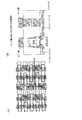
- FIG. 1 shows the layout of the 1st example of the floating gate type non-volatile memory arrangement configuration which embodies this invention.
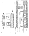
- FIG. 1 is a view showing the same layout as FIG. 1, and (B) and (C) are cross-sectional views in the word line direction and the bit line direction of a portion indicated by a dotted line in (A), respectively.
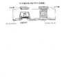
- (A) is a diagram showing the same layout as FIG. 1, and (B) is a cross-sectional view in the word line direction of a portion indicated by a dotted line in (A) (different from FIG. 2 (B)).
- FIG. 2 (B) shows the layout of the 1st example of the floating gate type non-volatile memory arrangement configuration which embodies this invention.
- FIG. 5 is a diagram illustrating a second method of forming a p-type layer immediately below the gate insulating film in addition to the first method of FIG. 4. It is a figure which illustrates the 3rd method by SOI (Silicon ⁇ > On> Insulator).
- (A) And (B) is a figure explaining the 2nd example of the floating gate type non-volatile memory arrangement configuration which embodies the present invention, and is equivalent to Drawing 2 (B) and Drawing 2 (C), respectively. It is sectional drawing of a word line direction and a bit line direction.
- FIG. 4 is a cross-sectional view in the word line direction corresponding to FIG.
- FIG. 2 is an equivalent circuit diagram of the floating gate nonvolatile memory layout shown in FIG. 1.
- 1 is a diagram illustrating a nonvolatile memory device having a conventional stack structure.
- FIG. (A) shows a pattern layout showing a conventional nonvolatile memory device
- (B) shows a cross-sectional view taken along line
- FIG. 1 is a diagram showing a layout. However, in an actual product, more cells are usually arranged in a matrix, but the layout of FIG. 1 shows a part of the layout (in the following description, a word line). Direction is row, bit line direction is column). Also, a decoder for switching the potential to the bit line and the word line is usually provided, but it is not shown.
- 2A is a diagram showing the same layout as FIG. 1, and FIG. 2B and FIG. 2C are the word line direction and the bit line at the locations indicated by the dotted lines in FIG. 2A, respectively.
- FIG. 3A is a diagram showing the same layout as FIG. 1, and FIG. 3B is a word line at a location indicated by a dotted line in FIG. 3A (different from FIG. 2B). It is sectional drawing of a direction.
- the structure of the floating gate type nonvolatile memory device is such that a memory FET sharing a floating gate and two transistors composed of a control gate portion are arranged side by side in the bit line direction. Configured. Each part such as a memory FET or a control gate part is separated by an element isolation region made of a thick oxide film.
- the control gate portion includes a control gate that faces the floating gate via a gate insulating film.
- a gate insulating film such as a silicon oxide film is grown, and a floating gate (polysilicon) is formed thereon. Deposit (deposit).
- the active region is “a portion where the silicon substrate is exposed” or “outside the element isolation region formed of a thick oxide film”.
- the gate insulating film (tunnel insulating film) of the memory FET is written and erased by hot carriers or FN current.
- the gate insulating film of the control gate portion is preferably manufactured by the same process using an insulating film made of the same material as the tunnel insulating film of the memory FET.
- the “tunnel insulating film” is used as a term meaning an insulating film in which writing and / or erasing is performed through this film during device operation.
- Such a tunnel insulating film is usually formed of a silicon oxide film of about 90 A (or a film in which nitrogen is slightly added). It is necessary to secure a certain film thickness in order to guarantee the data retention characteristics for 10 years. On the other hand, when the holding period may be short, the film thickness may be reduced and it is not necessary to be restricted by this film thickness.
- a floating gate (polysilicon) is formed on these insulating films so as to connect the memory FET and the control gate.
- the bit line extending in the length direction of the floating gate is formed of metal, and is connected to the source and drain (N + source / drain) of the memory FET through a contact (and silicide) penetrating the interlayer insulating film. Silicide is formed on the surface of the N + source / drain.
- the word line is formed by a buried word line separated from the substrate as will be described later.
- the buried word line (active layer word line) functions as a control gate. Inside the memory cell array, the word line does not have a contact from metal (thus, the area can be saved), and a potential is supplied outside the memory cell array.
- the “active layer” is used as a term meaning a portion other than the element isolation region (by a thick oxide film).
- the drain and source of the memory FET are formed by implantation (ion implantation).
- the side surface of the floating gate is formed with a sidewall spacer for LDD (Lightly Doped Drain) fabrication, and the floating gate is covered with silicide. This silicide and the silicide on the surface of the N + source / drain are simultaneously silicided and reduced in resistance by a normal process.
- LDD Lightly Doped Drain
- one word line (for example, w1) is arranged in a first row (cell 1, cell 3,%) Arranged in the vertical direction in the figure and a second row. (Cell 2, cell 4,...) Are shared.
- two rows sharing one word line use different bit lines (that is, the first row uses bit lines a1, a2, a3,..., The second row uses bit line b1). , B2...
- the cells adjacent to the word line direction (for example, the cell 1 and the cell 2) are arranged so that their floating gates are staggered laterally in the word line direction, that is, to the side of the mutual word line direction.
- control gates are typically offset by half the pitch so that the control gates are linearly aligned in the word line direction and in opposite directions (ie, in cell 1 the control gate is on the left side of the figure). In contrast, the cell 2 is shifted in the bit line direction (on the right side in the figure).
- the memory FET can be formed of either NMOS or PMOS, but is preferably formed of NMOS in the same manner as a normal nonvolatile memory because of carrier mobility, write characteristics, and the like.
- NMOS the substrate under the channel is p-type
- the source S and drain D are n +
- the floating gate (polysilicon) is n +.
- the operating condition of the memory cell with the layout illustrated in FIG. 1 is a NOR type.
- This memory cell basically operates in accordance with an existing floating gate type memory cell.
- typical operating conditions will be described.
- a negative (-) high voltage is applied to the control gate, a positive (+) high voltage is applied to the source electrode, and 0 V is applied to the drain electrode, and electrons are extracted from all floating gates.
- the drain is often floated in NOR-type erasure, but in the illustrated layout, the drain is shared by a plurality of cells, so that the drain is set to 0V.
- a constant voltage is applied to the drain electrode and a voltage about twice the drain voltage is applied to the control gate to determine whether a large amount of current flows.
- the read voltage can be arbitrarily determined based on the balance between speed and reliability. For example, a power supply voltage is applied to the gate and a low voltage is applied to the drain to prevent electrons from being injected into the floating gate due to a high voltage.
- the same potential as the drain is applied to the source of the cell sharing the drain in order to eliminate the current flowing in the direction other than the reading side.
- there are no electrons in the floating gate many electrons move between the source and drain (channel), and current flows.
- the number of electrons flowing through the channel is reduced.
- FIGS. 4 to 6 are cross-sectional views taken along the word line direction and the bit line direction, taken along the same location as FIG. Only the layout shown in FIG. 4A is the same as that shown in FIG. 1, but the layouts and cut portions in FIGS. 5 and 6 are also the same.
- FIGS. 4B and 4C are diagrams illustrating a first method in which the control gate portion is formed in the N well of the P substrate. When a positive voltage is applied as the control gate voltage, a positive voltage is applied to the entire N well (and the P + region), and when a negative voltage is applied, a negative voltage is applied to the p source / drain.
- FIGS. 5A and 5B are diagrams illustrating a second method of forming a p-type layer immediately below the gate insulating film in addition to the first method.
- a positive voltage is applied as the control gate voltage
- a positive voltage is applied to the entire N well
- a negative voltage is applied
- the resistance of the word line is lower than that in the first method.
- the p + layer is for applying a negative voltage to the control gate.
- the P + region is cut and formed like a source / drain region, but when erasing, a channel is formed under the floating gate and connected to each other.
- a continuous P + region is formed in FIG.
- FIGS. 6A and 6B are diagrams illustrating a third method using SOI (Silicon On On Insulator). Each node is formed on an oxide film as an insulating film.
- the control gate portion can be easily insulated from other nodes, and the impurity type of the control gate portion can be arbitrarily set.
- a gate voltage is applied to the substrate of the control gate part insulated by the oxide film.
- FIGS. 7A, 7B, and 8 are diagrams illustrating a second example of a floating gate type nonvolatile memory arrangement configuration embodying the present invention.
- 7A and 7B are cross-sectional views in the word line direction and the bit line direction corresponding to FIGS. 2B and 2C, respectively.
- FIG. 8 is a cross-sectional view in the word line direction corresponding to FIG.
- the second example illustrated in FIGS. 7A and 7B and FIG. 8 differs from the first example described above only in the configuration of the floating gate and the gate insulating film.
- the gate insulating film (tunnel insulating film) of the memory FET is written and erased by hot carriers or FN current.
- the gate insulating film of the control gate portion is composed of two layers of a gate insulating film A (an insulating film made of the same material as the tunnel insulating film) and a gate insulating film B (High-k insulating film).
- the tunnel insulating film which is indispensable for realizing the non-volatile memory, and the high-k insulating film already possessed by the logic process are combined to suppress the leakage current while maintaining the capacity (high capacity) ⁇ Low leakage).
- the exemplary two-layer structure can realize a non-volatile memory with a minimum process change from a normal logic CMOS process (using a high-k insulating film).
- the floating gate is configured by integrally connecting the gate electrode a, the gate electrode b, and the gate electrode c.
- a gate electrode b made of metal or polysilicon is formed on the gate insulating film B (high-k insulating film).
- a gate electrode a is formed on the memory FET.
- the gate electrode c (polysilicon) is used to connect the memory FET and the control gate.
- the gate electrode b is a metal
- the impurity type of the gate electrode c does not matter.
- depositing a thin metal gate directly on a high-k gate insulating film and depositing a thick polysilicon on the thin metal gate makes it possible to use an arbitrary work function of the metal gate and ease the processing of the polysilicon. It is taken into consideration.
- FIG. 9 is an equivalent circuit diagram of the floating gate type nonvolatile memory layout shown in FIG. However, the layout shown in FIG. 1 is illustrated by an arrangement rotated 90 degrees. As shown in the figure, a virtual cell ground memory cell array configuration is realized. The upper and lower memory cell rows in the figure sharing the same word line use different bit lines. The word line is efficiently shared between the upper and lower cells.
- the number of contacts per cell can be reduced by adopting a virtual ground type cell array (1/2 for the drain and 1/2 for the source, one total). If the configuration is not a virtual ground type, a single contact for each drain and source, or even if only the source contact can be shared with other cells, a total of 1.5 to 2 contacts per cell is required. Considering the space for separating it from other nodes, the area is greatly increased.
- the word line by the active layer is adopted, but the layout is devised (adjacent cells are shifted by half the pitch so that the protrusions of the floating gates protrude from each other area) Since the cells share the word lines, the area of the word lines per cell is reduced.
- the area required (to form a word line) is the product of half the minimum active layer width and the contact pitch (minimum pitch when floating gates and contacts are alternately arranged).
- the active layer word line is not used, a large area is required to contact the active layer in addition to the metal wiring of the word line.
- each cell requires an active layer and an area for separating it from the facing cell is also required. The area will increase.
Landscapes
- Non-Volatile Memory (AREA)
- Semiconductor Memories (AREA)
Abstract
本発明は、仮想接地型によるメモリセルアレイ構成を実現し、安価なプロセスでなおかつ省面積なメモリセルアレイを実現する。行列状に配置した浮遊ゲート型不揮発性メモリ装置のそれぞれが、浮遊ゲートを共有するメモリFETと制御ゲート部からなる2トランジスタにより構成され、その制御ゲート部は浮遊ゲートに対してゲート絶縁膜を介して対峙する制御ゲートを含む。ビット線は、浮遊ゲートの上方をその長さ方向に伸び、かつ、制御ゲートとして機能するワード線が、ビット線と直交方向に伸びる。同じワード線を共有しかつワード線方向に隣り合うセルは、それぞれの浮遊ゲートが互いの領域に出っ張るようピッチの半分ずつずらして、かつ、互いに反対向きに配置する。
Description
本発明は、複数個のセルをワード線方向及びビット線方向の行列状に配置した浮遊ゲート型不揮発性メモリ配置構成に関する。
不揮発性メモリとして、スタック型浮遊ゲート構造が知られている。図10は、特許文献1に記載の従来のスタック構造を有する不揮発性メモリ装置を示す図である。薄い酸化シリコン膜からなるゲート絶縁膜およびソース、ドレイン領域がシリコン基板上に形成され、ゲート絶縁膜の上には多結晶シリコン膜からなる浮遊ゲート電極、層間絶縁膜および多結晶シリコン膜からなる制御ゲート電極が順次積層されている。図示の不揮発性メモリ装置は、浮遊ゲート電極に電荷を蓄積したり、浮遊ゲート電極から電荷を放出したりすることによって、情報の書き込み、保持および消去が行なわれる。メモリチップで通常用いられている構造であるため、プロセス及びデバイスともよく知られている。浮遊ゲート電極の上方に制御ゲート電極を積層する構造のために高密度である。しかし、一層目の多結晶シリコン膜(ポリシリコン)で浮遊ゲート電極を形成し、かつこの浮遊ゲート電極から層間絶縁膜によって隔離される2層目の多結晶シリコン膜で制御ゲート電極を形成するため、製造プロセスが複雑になり、コスト的に不利である。
このために、1層の多結晶シリコン膜を用いて、浮遊ゲート電極を構成すると共に、制御ゲート電極を拡散領域により形成した不揮発性メモリが知られている(特許文献2,3参照)。図11(A)は、特許文献2に記載の従来の不揮発性メモリ装置を示すパターンレイアウトを、図11(B)はX-X線に沿う断面図を示している。
シリコン基板表面の素子領域にはソ―ス、ドレイン領域を含むメモリFETと、制御ゲート用拡散領域が形成されている。ソ―ス,ドレイン領域間のチャネル領域上及び制御ゲート用拡散領域の一部上にはそれぞれ極薄酸化膜a、bを介して浮遊ゲ―トが形成されている。また、ドレイン領域とビット線用拡散領域間のチャネル領域上にはゲ―ト酸化膜を介してセレクトゲ―トを形成したセレクトトランジスタが設けられている。更に、全面に堆積されたCVD酸化膜上には、ソ―ス領域とコンタクトホ―ルaを介して接続する共通電位線、及びビット線用拡散領域とコンタクトホ―ルbを介して接続するビット線が形成されている。
このような不揮発性メモリにおいて、消去は制御ゲート用拡散領域を高電位、ドレイン領域を0Vとし、浮遊ゲ―トに電荷を蓄積させることにより行なう。また、書き込みは制御ゲート用拡散領域を0V、ドレイン領域を高電位とし、浮遊ゲ―トからドレイン領域へ電荷を流出させることにより行なう。
図示の不揮発性メモリ装置は、浮遊ゲート電極のみを一層の多結晶シリコン膜で形成するものであるために、製造プロセスが簡単になるが、制御ゲート電極を浮遊ゲート電極の上方ではなく、側方に配置するために、セル面積が大きくなるという問題がある。
一方、仮想接地型の不揮発性メモリが周知である(特許文献4参照)。仮想接地型の不揮発性メモリは、ソースとドレインを入れ替えて対称的に動作させるよう構成することにより、メモリセルの集積密度を高めることができる。
本発明は、係る問題点を解決して、浮遊ゲートを共有する制御ゲート部をメモリFETの側方に配置した浮遊ゲート型不揮発性メモリにおいて仮想接地型(virtual ground)によるメモリセルアレイ構成を実現し、安価なプロセスでなおかつ省面積なメモリセルアレイを実現することを目的としている。
本発明は、1個の浮遊ゲート型不揮発性メモリ装置を1個のセルとして、複数個のセルをワード線方向及びビット線方向の行列状に配置した浮遊ゲート型不揮発性メモリ配置構成において、前記1個の浮遊ゲート型不揮発性メモリ装置は、浮遊ゲートを共有するメモリFETと制御ゲート部からなる2トランジスタを半導体基板の上に併置して構成され、該制御ゲート部は前記浮遊ゲートに対してゲート絶縁膜を介して対峙する制御ゲートを含む。ビット線は、前記浮遊ゲートの上方をその長さ方向に伸び、かつ、前記制御ゲートとして機能する前記ワード線が、前記ビット線と直交方向に伸びる。同じワード線を共有しかつワード線方向に隣り合うセルは、互いに反対向きにかつビット線方向にずらして配置し、かつ、この隣り合うセルの制御ゲートがワード線方向に直線状に並ぶようにワード線方向に隣り合うセルの浮遊ゲートをワード線方向の側方に互い違いに配置した。同じワード線を共有する2つのセル行は、互いに異なるビット線を使用する。ワード線は、半導体基板と分離した埋め込みワード線によって形成されて、メモリ配置構成の内部ではメタルからコンタクトを持たず、メモリ配置構成の外側で電位を供給される。複数個のセルは、仮想接地型によるメモリ配置構成を実現する。
本発明によれば、仮想接地型(virtual ground)によるメモリセルアレイ構成を実現し、安価なプロセスでなおかつ省面積なメモリセルアレイを実現することができる。さらに、アクティブ層によるワード線を採用し、かつ、隣り合うセルのピッチをずらして配置し、浮遊ゲートを互いの領域のワード線方向の側方に互い違いに配置して、対面のセル同士がワード線を分け合うことにより、セル当たりのワード線の面積を減らすことができる。
以下、例示に基づき本発明を説明する。本発明を具体化する浮遊ゲート型不揮発性メモリ配置構成の第1の例を、図1~図6を参照して説明する。図1は、レイアウトを示す図である。但し、実際の製品においては、より多くのセルが行列状に配置されるのが通常であるが、図1のレイアウトは、その一部を取り出して図示している(以下の説明において、ワード線方向を行、ビット線方向を列とする)。また、ビット線及びワード線に電位を切り換え供給するデコーダが通常に備えられるが、図示省略している。図2(A)は図1と同一のレイアウトを示す図であり、図2(B)及び図2(C)は、それぞれ図2(A)中に点線で示す箇所のワード線方向及びビット線方向の断面図である。図3(A)は、図1と同一のレイアウトを示す図であり、図3(B)は、図3(A)中に点線で示す(図2(B)とは異なる)箇所のワード線方向の断面図である。
浮遊ゲート型不揮発性メモリ装置の構成は、特に、図2(C)に見られるように、浮遊ゲートを共有するメモリFETと制御ゲート部からなる2トランジスタをビット線方向に互いに側方に併置して構成される。メモリFETとか制御ゲート部等の各部は、厚い酸化膜による素子分離領域により分離されている。制御ゲート部は、浮遊ゲートに対してゲート絶縁膜を介して対峙する制御ゲートを含んでいる。この浮遊ゲート型不揮発性メモリ装置は、半導体基板にアクティブ領域を形成した後、例えばシリコン酸化膜のようなゲート絶縁膜(トンネル絶縁膜)を成長させ、その上に、浮遊ゲート(ポリシリコン)をデポジション(堆積)する。アクティブ領域は、周知のように、「シリコン基板が露出された部分」、もしくは「厚い酸化膜で形成された素子分離領域の外側」である。メモリFETのゲート絶縁膜(トンネル絶縁膜)は、ホットキャリアもしくはFN電流にて書き込み及び消去を行なう。制御ゲート部のゲート絶縁膜は、メモリFETのトンネル絶縁膜と同材質の絶縁膜により同一プロセスで作製することが望ましい。なお、本明細書において、「トンネル絶縁膜」とは、デバイス動作の上でこの膜を通して書き込み且つ/又は消去を行なう絶縁膜を意味する用語として用いている。このようなトンネル絶縁膜は、通常90A程度のシリコン酸化膜(もしくはそれに窒素を若干付加したもの)で形成される。10年間のデータ保持特性を保証するためにある程度の膜厚を確保する必要がある。逆に、保持期間が短くてよい場合は薄膜化してもよく、この膜厚に縛られる必要は無い。
これら絶縁膜の上に、浮遊ゲート(ポリシリコン)を、メモリFETと制御ゲートを接続するようにして作製する。浮遊ゲートの長さ方向に伸びるビット線はメタルで形成され、層間絶縁膜を貫通するコンタクト(及びシリサイド)を通じてメモリFETのソースとドレイン(N+ソース・ドレイン)に接続される。N+ソース・ドレインの表面にシリサイドが形成されている。ワード線は、後述するように基板と分離した埋め込みワード線によって形成される。埋め込みワード線(アクティブ層ワード線)は、制御ゲートとして機能する。メモリセルアレイ内部ではワード線はメタルからコンタクトを持たず(それ故、省面積化が可能になっている)、メモリセルアレイの外側で電位を供給されることになる。なお、本明細書において、「アクティブ層」とは、(厚い酸化膜による)素子分離領域以外の部分を意味する用語として用いている。
これによって、制御ゲート-浮遊ゲート-チャネルという接続で形成できる不揮発性メモリ構造を構成することができる。この後、インプラ(イオンインプランテーション)によって、メモリFETのドレイン及びソースを作成する。また、通常の技術に従い、図2(C)に示すように、浮遊ゲート側面はLDD(Lightly Doped Drain)作製用のサイドウォールスペーサを作成し、かつ、浮遊ゲートの上方はシリサイドで覆う。このシリサイドと、上述のN+ソース・ドレインの表面のシリサイドは、通常のプロセスにより同時にシリサイド化され低抵抗化される。
特に、図1に見られるように、1本のワード線(例えば、w1)を、図中の縦方向に並ぶ第1の行(セル1,セル3,・・・)と、第2の行(セル2,セル4,・・・)が共有している。但し、1本のワード線を共有する2つの行は、互いに異なるビット線を使用する(即ち、第1の行はビット線a1、a2、a3・・・を、第2の行はビット線b1、b2・・・を使用する)。そして、ワード線方向に隣り合うセル(例えばセル1とセル2)は、それぞれの浮遊ゲートをワード線方向の側方に互い違いに、即ち、互いの領域のワード線方向の側方にまでビット線方向に出っ張らせて、制御ゲートがワード線方向に直線状に並ぶように典型的にはピッチの半分ずつずらして、かつ、互いに反対向きに(即ち、セル1では制御ゲートが図中の左側であるのに対して、セル2では図中の右側に)ビット線方向にずらして配置している。このような配置によって、詳細は図9を参照して後述するように、セル当たりのワード線の面積を減らして、省面積なメモリセルアレイを実現することができる。
メモリFETは、NMOS或いはPMOSのいずれでも形成することができるが、キャリアの移動度や書き込み特性などから、通常の不揮発性メモリと同様にNMOSで形成することが望ましい。NMOSで形成する場合、チャネル下の基板はp型、ソースS及びドレインDはn+、浮遊ゲート(ポリシリコン)はn+である。
図1に例示したレイアウトのメモリセルの動作条件は、NOR型である。このメモリセルは、基本的に既存の浮遊ゲート型メモリセルに準じて動作する。以下、典型的な動作条件について説明する。書き込み時には、制御ゲートとメモリFETのドレイン電極に高電圧をかけて、メモリFETのソースとドレインの間を流れる電子を高エネルギーにすると、電子は、ゲート絶縁膜(トンネル絶縁膜)を突き破って浮遊ゲートに飛び込む。
データの消去は、制御ゲートに負(-)の高電圧、ソース電極に正(+)の高電圧、ドレイン電極に0Vを印加して、すべての浮遊ゲートから、電子を抜き出す。通常NOR型の消去ではドレインを浮かせることが多いが、例示のレイアウトではドレインを複数のセルで共有するため0Vとする。
データを読み出すときは、ドレイン電極に一定の電圧を、制御ゲートにドレイン電圧の約2倍の電圧をかけて、電流が多く流れるか否かを判別する。読み出しの電圧は、速度と信頼性との兼ね合いから任意に決定できる。例えば、ゲートには電源電圧を、ドレインには、高電圧により電子が浮遊ゲートに注入されるのを防ぐためある程度低い電圧を印加する。例示のレイアウトでは、ドレインを共有しているセルのうち、読み出す側でない方向への電流をなくすために、そのソースにドレインと同電位を与える。浮遊ゲートに電子がない状態では、ソースとドレインの間(チャネル)で多くの電子が移動し電流が流れる。一方、浮遊ゲートに電子がある状態では、チャネルを流れる電子が少なくなる。
次に、メモリFETは、NMOS又はPMOSのいずれで形成することも可能であるが、以下、NMOSで形成した場合を例として、制御ゲート(ワード線)電圧の印加について、図4~図6を参照して説明する。図4~図6は、いずれも、図2と同じ箇所で切断したワード線方向及びビット線方向の断面図である。図4(A)のみに、図1に示したのと同一のレイアウトを示しているが、図5及び図6のレイアウト及び切断箇所も同一のものである。図4(B)及び(C)は、制御ゲート部を、P基板のNウェル内に形成した第1の方法を例示する図である。制御ゲート電圧として正電圧を与える場合はNウェル全体(とP+領域)に正電圧を印加し、負電圧を与える場合はpソース・ドレインに負電圧を印加する。
図5(A)及び(B)は、上記の第1の方法に追加して、ゲート絶縁膜の直ぐ下にp型層を形成する第2の方法を例示する図である。制御ゲート電圧として正電圧を与える場合はNウェル全体に正電圧を印加し、負電圧を与える場合はp型層に負電圧を印加する。上記の第1の方法よりもワード線の抵抗が低くなる。
図4及び図5において、p+層は、制御ゲートに負電圧を与えるためのものである。図4(B)ではP+領域がソース・ドレイン領域のように切断されて形成されているが、消去の際には浮遊ゲート下にチャネルを形成して相互に接続されることになる。これに対して、図5(A)では連続したP+領域が形成されている。典型的なNOR型の動作条件では消去時に制御ゲートに負電圧を与える必要があるが、Nウェルの電位はP基板より低くできないので、負電圧を与えるためにはNウェルの中にP型の領域を定義する必要がある。
図6(A)及び(B)は、SOI(Silicon On Insulator)による第3の方法を例示する図である。絶縁膜としての酸化膜の上に、各ノードを形成する。制御ゲート部は他のノードから容易に絶縁でき、また、制御ゲート部の不純物型は任意に設定できる。ゲート電圧を、酸化膜で絶縁された制御ゲート部の基板に印加する。
図7(A)(B)及び図8は、本発明を具体化する浮遊ゲート型不揮発性メモリ配置構成の第2の例を説明する図である。図7(A)及び(B)は、それぞれ図2(B)及び(C)に相当するワード線方向及びビット線方向の断面図である。また、図8は、図3(B)に相当するワード線方向の断面図である。図7(A)及び(B)及び図8に例示の第2の例は、上述の第1の例とは、浮遊ゲート及びゲート絶縁膜の構成のみを異にしている。
図7(A)及び(B)及び図8に示す浮遊ゲート型メモリセルにおいて、メモリFETのゲート絶縁膜(トンネル絶縁膜)は、ホットキャリアもしくはFN電流にて書き込み及び消去を行なう。制御ゲート部のゲート絶縁膜は、ゲート絶縁膜A(トンネル絶縁膜と同材質の絶縁膜)とゲート絶縁膜B(High-k絶縁膜)の2層により構成される。図示の構成は、不揮発性メモリを実現するのに必須のトンネル絶縁膜と、ロジックプロセスが既に持っているhigh-k絶縁膜を組み合わせることにより、容量を保ったままリーク電流を抑えること(高容量・低リーク)ができる。これにより安定した書き込み及び消去と電荷の長期保存が可能になる。例示の2層構造は(high-k絶縁膜を用いた)通常のロジックCMOSのプロセスから最小限のプロセス変更によって不揮発性メモリを実現することができる。
浮遊ゲートは、ゲート電極a,ゲート電極b,ゲート電極cを一体に接続して構成する。制御ゲート部上では、ゲート絶縁膜B(high-k絶縁膜)上に、金属或いはポリシリコンからなるゲート電極bを形成する。メモリFET上には、ゲート電極aを形成する。さらに、ゲート電極c(ポリシリコン)をメモリFETと制御ゲートを接続するために使っている。ゲート電極bが金属の場合、ゲート電極c(ポリシリコン)の不純物型は問題にならない。ここで、薄い金属ゲートをhigh-kゲート絶縁膜直上に堆積し、その上に厚いポリシリコンを堆積することは、金属ゲートの任意の仕事関数を利用できることと、ポリシリコンの加工し易さを考慮したものである。
図9は、図1に示す浮遊ゲート型不揮発性メモリレイアウトの等価回路図である。但し、図1に示すレイアウトとは90度回転した配置で例示している。図示のように、仮想接地型(virtual ground)によるメモリセルアレイ構成を実現している。同じワード線を共有する図中の上下のメモリセル行が、互いに異なるビット線を使用する。ワード線は、上下のセルで効率よく共有されている。
本発明は、仮想接地型のセルアレイを採用することによって、セル当たりのコンタクトの数を減らすことができる(ドレインに1/2、ソースに1/2、計1個)。仮想接地型でない構成だと、ドレインとソースに各1個のコンタクト、もしくはソースコンタクトのみを他のセルと共有できるとしてもセル当たり計1.5~2個のコンタクトが必要となり、そのコンタクト自身の面積、またそれを他のノードから切り離すスペースを考慮すると大きな面積の増加になる。
さらに、アクティブ層によるワード線を採用するが、レイアウトの工夫(隣り合うセルをピッチの半分ずつずらして配置し、浮遊ゲートの突起がお互いの領域に出っ張れるようにする)を行い、対面のセル同士がワード線を分け合うことにより、セル当たりのワード線の面積を減らしている。(ワード線を形成するのに)必要な面積はアクティブ層最小幅の半分とコンタクトピッチ(浮遊ゲートとコンタクトを交互に配置する場合の最小ピッチ)の積となる。アクティブ層ワード線を用いない場合、ワード線のメタル配線に加え、それからアクティブ層にコンタクトするための大きな面積が必要となる。またアクティブ層によるワード線を用いても、本レイアウトのようにワード線を対面で分け合う工夫がない場合、各セルでアクティブ層を必要としそれを対面のセルから分離する面積も必要となるので、面積が増加することになる。
以上、本開示にて幾つかの実施の形態を単に例示として詳細に説明したが、本発明の新規な教示及び有利な効果から実質的に逸脱せずに、その実施の形態には多くの改変例が可能である。
Claims (7)
- 1個の浮遊ゲート型不揮発性メモリ装置を1個のセルとして、複数個のセルをワード線方向及びビット線方向の行列状に配置した浮遊ゲート型不揮発性メモリ配置構成において、
前記1個の浮遊ゲート型不揮発性メモリ装置は、浮遊ゲートを共有するメモリFETと制御ゲート部からなる2トランジスタを半導体基板の上に併置して構成され、該制御ゲート部は前記浮遊ゲートに対してゲート絶縁膜を介して対峙する制御ゲートを含み、
前記ビット線は、前記浮遊ゲートの上方をその長さ方向に伸び、かつ、前記制御ゲートとして機能する前記ワード線が、前記ビット線と直交方向に伸び、
同じワード線を共有しかつワード線方向に隣り合うセルは、互いに反対向きにかつビット線方向にずらして配置し、かつ、この隣り合うセルの制御ゲートがワード線方向に直線状に並ぶようにワード線方向に隣り合うセルの浮遊ゲートをワード線方向の側方に互い違いに配置したことから成る浮遊ゲート型不揮発性メモリ配置構成。 - 同じワード線を共有する2つのセル行が、互いに異なるビット線を使用する請求項1に記載の浮遊ゲート型不揮発性メモリ配置構成。
- 前記ワード線は、半導体基板と分離した埋め込みワード線によって形成されて、メモリ配置構成の内部ではメタルからコンタクトを持たず、メモリ配置構成の外側で電位を供給される請求項1に記載の浮遊ゲート型不揮発性メモリ配置構成。
- 前記制御ゲートを、半導体基板と逆導電型のウェル内に形成した請求項3に記載の浮遊ゲート型不揮発性メモリ配置構成。
- 前記ウェルとは逆導電型の層を、ゲート絶縁膜の直ぐ下に形成した請求項4に記載の浮遊ゲート型不揮発性メモリ配置構成。
- 前記制御ゲートを他のノードから絶縁するように、絶縁膜の上に制御ゲートを形成し、ゲート電圧を絶縁膜で絶縁された制御ゲートに印加する請求項3に記載の浮遊ゲート型不揮発性メモリ配置構成。
- 前記複数個のセルは、仮想接地型によるメモリ配置構成を実現した請求項1に記載の浮遊ゲート型不揮発性メモリ配置構成。
Priority Applications (1)
| Application Number | Priority Date | Filing Date | Title |
|---|---|---|---|
| JP2010531734A JPWO2010038426A1 (ja) | 2008-09-30 | 2009-09-29 | 浮遊ゲート型不揮発性メモリ配置構成 |
Applications Claiming Priority (2)
| Application Number | Priority Date | Filing Date | Title |
|---|---|---|---|
| JP2008-255297 | 2008-09-30 | ||
| JP2008255297 | 2008-09-30 |
Publications (1)
| Publication Number | Publication Date |
|---|---|
| WO2010038426A1 true WO2010038426A1 (ja) | 2010-04-08 |
Family
ID=42073208
Family Applications (1)
| Application Number | Title | Priority Date | Filing Date |
|---|---|---|---|
| PCT/JP2009/004989 Ceased WO2010038426A1 (ja) | 2008-09-30 | 2009-09-29 | 浮遊ゲート型不揮発性メモリ配置構成 |
Country Status (3)
| Country | Link |
|---|---|
| JP (1) | JPWO2010038426A1 (ja) |
| TW (1) | TWI416713B (ja) |
| WO (1) | WO2010038426A1 (ja) |
Families Citing this family (1)
| Publication number | Priority date | Publication date | Assignee | Title |
|---|---|---|---|---|
| US9634019B1 (en) * | 2015-10-01 | 2017-04-25 | Silicon Storage Technology, Inc. | Non-volatile split gate memory cells with integrated high K metal gate, and method of making same |
Citations (4)
| Publication number | Priority date | Publication date | Assignee | Title |
|---|---|---|---|---|
| JP2004363260A (ja) * | 2003-06-04 | 2004-12-24 | Matsushita Electric Ind Co Ltd | 不揮発性半導体記憶装置 |
| JP2005522884A (ja) * | 2002-04-15 | 2005-07-28 | エスティマイクロエレクトロニクス エスエー | 半導体メモリ・デバイス |
| JP2005533372A (ja) * | 2002-07-09 | 2005-11-04 | インピンジ インコーポレイテッド | フローティング・ゲート半導体構造 |
| JP2007184321A (ja) * | 2006-01-04 | 2007-07-19 | Toshiba Corp | 半導体装置と半導体システム |
-
2009
- 2009-09-24 TW TW098132314A patent/TWI416713B/zh not_active IP Right Cessation
- 2009-09-29 WO PCT/JP2009/004989 patent/WO2010038426A1/ja not_active Ceased
- 2009-09-29 JP JP2010531734A patent/JPWO2010038426A1/ja active Pending
Patent Citations (4)
| Publication number | Priority date | Publication date | Assignee | Title |
|---|---|---|---|---|
| JP2005522884A (ja) * | 2002-04-15 | 2005-07-28 | エスティマイクロエレクトロニクス エスエー | 半導体メモリ・デバイス |
| JP2005533372A (ja) * | 2002-07-09 | 2005-11-04 | インピンジ インコーポレイテッド | フローティング・ゲート半導体構造 |
| JP2004363260A (ja) * | 2003-06-04 | 2004-12-24 | Matsushita Electric Ind Co Ltd | 不揮発性半導体記憶装置 |
| JP2007184321A (ja) * | 2006-01-04 | 2007-07-19 | Toshiba Corp | 半導体装置と半導体システム |
Also Published As
| Publication number | Publication date |
|---|---|
| JPWO2010038426A1 (ja) | 2012-03-01 |
| TWI416713B (zh) | 2013-11-21 |
| TW201023349A (en) | 2010-06-16 |
Similar Documents
| Publication | Publication Date | Title |
|---|---|---|
| JP4246400B2 (ja) | 半導体記憶装置 | |
| TWI845305B (zh) | 非揮發性記憶裝置 | |
| KR100334300B1 (ko) | 불휘발성반도체기억장치및그제조방법 | |
| JP3238576B2 (ja) | 不揮発性半導体記憶装置 | |
| JP2817500B2 (ja) | 不揮発性半導体記憶装置 | |
| TWI433302B (zh) | 積體電路自對準三度空間記憶陣列及其製作方法 | |
| US20120235224A1 (en) | Circuit and Method for a Three Dimensional Non-Volatile Memory | |
| JPWO2000070683A1 (ja) | 半導体記憶装置 | |
| JP2006093695A (ja) | 不揮発性メモリ素子及びその形成方法 | |
| JP3472313B2 (ja) | 不揮発性記憶装置 | |
| US9287284B2 (en) | Semiconductor field-effect transistor, memory cell and memory device | |
| JP2009130136A (ja) | 不揮発性半導体記憶装置およびその製造方法 | |
| JP2008294088A (ja) | 半導体装置およびその製造方法 | |
| CN100573917C (zh) | 半导体存储器元件 | |
| US7745872B2 (en) | Asymmetric operation method of non-volatile memory structure | |
| US10388660B2 (en) | Semiconductor device and method for manufacturing the same | |
| US20070045715A1 (en) | Semiconductor storage device | |
| KR20080001644A (ko) | 전하 축적층을 갖는 mis 트랜지스터를 구비한 반도체기억 장치 | |
| WO2010038426A1 (ja) | 浮遊ゲート型不揮発性メモリ配置構成 | |
| US7388253B2 (en) | Nonvolatile memory | |
| JP2009164349A (ja) | 不揮発性半導体記憶装置及びその製造方法 | |
| JPWO2009096083A1 (ja) | 浮遊ゲート型不揮発性メモリ装置及びその製造方法 | |
| JP2006344735A (ja) | 半導体装置 | |
| JP7462389B2 (ja) | 不揮発性半導体記憶装置 | |
| US20090140316A1 (en) | Semiconductor memory device and method of fabricating the same |
Legal Events
| Date | Code | Title | Description |
|---|---|---|---|
| 121 | Ep: the epo has been informed by wipo that ep was designated in this application |
Ref document number: 09817468 Country of ref document: EP Kind code of ref document: A1 |
|
| WWE | Wipo information: entry into national phase |
Ref document number: 2010531734 Country of ref document: JP |
|
| NENP | Non-entry into the national phase |
Ref country code: DE |
|
| 122 | Ep: pct application non-entry in european phase |
Ref document number: 09817468 Country of ref document: EP Kind code of ref document: A1 |