WO2010007985A1 - 点灯装置、バックライト装置 - Google Patents
点灯装置、バックライト装置 Download PDFInfo
- Publication number
- WO2010007985A1 WO2010007985A1 PCT/JP2009/062733 JP2009062733W WO2010007985A1 WO 2010007985 A1 WO2010007985 A1 WO 2010007985A1 JP 2009062733 W JP2009062733 W JP 2009062733W WO 2010007985 A1 WO2010007985 A1 WO 2010007985A1
- Authority
- WO
- WIPO (PCT)
- Prior art keywords
- circuit
- lighting
- output
- signal
- voltage
- Prior art date
Links
Images


Classifications
-
- H—ELECTRICITY
- H05—ELECTRIC TECHNIQUES NOT OTHERWISE PROVIDED FOR
- H05B—ELECTRIC HEATING; ELECTRIC LIGHT SOURCES NOT OTHERWISE PROVIDED FOR; CIRCUIT ARRANGEMENTS FOR ELECTRIC LIGHT SOURCES, IN GENERAL
- H05B41/00—Circuit arrangements or apparatus for igniting or operating discharge lamps
- H05B41/14—Circuit arrangements
- H05B41/26—Circuit arrangements in which the lamp is fed by power derived from dc by means of a converter, e.g. by high-voltage dc
- H05B41/28—Circuit arrangements in which the lamp is fed by power derived from dc by means of a converter, e.g. by high-voltage dc using static converters
- H05B41/282—Circuit arrangements in which the lamp is fed by power derived from dc by means of a converter, e.g. by high-voltage dc using static converters with semiconductor devices
- H05B41/2825—Circuit arrangements in which the lamp is fed by power derived from dc by means of a converter, e.g. by high-voltage dc using static converters with semiconductor devices by means of a bridge converter in the final stage
- H05B41/2828—Circuit arrangements in which the lamp is fed by power derived from dc by means of a converter, e.g. by high-voltage dc using static converters with semiconductor devices by means of a bridge converter in the final stage using control circuits for the switching elements
-
- H—ELECTRICITY
- H05—ELECTRIC TECHNIQUES NOT OTHERWISE PROVIDED FOR
- H05B—ELECTRIC HEATING; ELECTRIC LIGHT SOURCES NOT OTHERWISE PROVIDED FOR; CIRCUIT ARRANGEMENTS FOR ELECTRIC LIGHT SOURCES, IN GENERAL
- H05B41/00—Circuit arrangements or apparatus for igniting or operating discharge lamps
- H05B41/14—Circuit arrangements
- H05B41/36—Controlling
- H05B41/38—Controlling the intensity of light
- H05B41/39—Controlling the intensity of light continuously
- H05B41/392—Controlling the intensity of light continuously using semiconductor devices, e.g. thyristor
- H05B41/3921—Controlling the intensity of light continuously using semiconductor devices, e.g. thyristor with possibility of light intensity variations
- H05B41/3927—Controlling the intensity of light continuously using semiconductor devices, e.g. thyristor with possibility of light intensity variations by pulse width modulation
-
- H—ELECTRICITY
- H05—ELECTRIC TECHNIQUES NOT OTHERWISE PROVIDED FOR
- H05B—ELECTRIC HEATING; ELECTRIC LIGHT SOURCES NOT OTHERWISE PROVIDED FOR; CIRCUIT ARRANGEMENTS FOR ELECTRIC LIGHT SOURCES, IN GENERAL
- H05B45/00—Circuit arrangements for operating light-emitting diodes [LED]
- H05B45/10—Controlling the intensity of the light
-
- H—ELECTRICITY
- H05—ELECTRIC TECHNIQUES NOT OTHERWISE PROVIDED FOR
- H05B—ELECTRIC HEATING; ELECTRIC LIGHT SOURCES NOT OTHERWISE PROVIDED FOR; CIRCUIT ARRANGEMENTS FOR ELECTRIC LIGHT SOURCES, IN GENERAL
- H05B45/00—Circuit arrangements for operating light-emitting diodes [LED]
- H05B45/30—Driver circuits
- H05B45/37—Converter circuits
- H05B45/3725—Switched mode power supply [SMPS]
- H05B45/382—Switched mode power supply [SMPS] with galvanic isolation between input and output
-
- H—ELECTRICITY
- H05—ELECTRIC TECHNIQUES NOT OTHERWISE PROVIDED FOR
- H05B—ELECTRIC HEATING; ELECTRIC LIGHT SOURCES NOT OTHERWISE PROVIDED FOR; CIRCUIT ARRANGEMENTS FOR ELECTRIC LIGHT SOURCES, IN GENERAL
- H05B45/00—Circuit arrangements for operating light-emitting diodes [LED]
- H05B45/30—Driver circuits
- H05B45/37—Converter circuits
- H05B45/3725—Switched mode power supply [SMPS]
- H05B45/39—Circuits containing inverter bridges
-
- Y—GENERAL TAGGING OF NEW TECHNOLOGICAL DEVELOPMENTS; GENERAL TAGGING OF CROSS-SECTIONAL TECHNOLOGIES SPANNING OVER SEVERAL SECTIONS OF THE IPC; TECHNICAL SUBJECTS COVERED BY FORMER USPC CROSS-REFERENCE ART COLLECTIONS [XRACs] AND DIGESTS
- Y02—TECHNOLOGIES OR APPLICATIONS FOR MITIGATION OR ADAPTATION AGAINST CLIMATE CHANGE
- Y02B—CLIMATE CHANGE MITIGATION TECHNOLOGIES RELATED TO BUILDINGS, e.g. HOUSING, HOUSE APPLIANCES OR RELATED END-USER APPLICATIONS
- Y02B20/00—Energy efficient lighting technologies, e.g. halogen lamps or gas discharge lamps
- Y02B20/30—Semiconductor lamps, e.g. solid state lamps [SSL] light emitting diodes [LED] or organic LED [OLED]
-
- Y—GENERAL TAGGING OF NEW TECHNOLOGICAL DEVELOPMENTS; GENERAL TAGGING OF CROSS-SECTIONAL TECHNOLOGIES SPANNING OVER SEVERAL SECTIONS OF THE IPC; TECHNICAL SUBJECTS COVERED BY FORMER USPC CROSS-REFERENCE ART COLLECTIONS [XRACs] AND DIGESTS
- Y10—TECHNICAL SUBJECTS COVERED BY FORMER USPC
- Y10S—TECHNICAL SUBJECTS COVERED BY FORMER USPC CROSS-REFERENCE ART COLLECTIONS [XRACs] AND DIGESTS
- Y10S315/00—Electric lamp and discharge devices: systems
- Y10S315/04—Dimming circuit for fluorescent lamps
Definitions
- the present invention relates to a lighting device used for a backlight device of a liquid crystal display device, and more particularly to reduction of light flicker and improvement of circuit efficiency.
- Liquid crystal display devices generally display images using light from a backlight device in which a plurality of fluorescent lamps such as cold cathode lamps are lit.
- An inverter circuit is generally used for a fluorescent lamp lighting circuit. By lighting the lamp at a high frequency, the luminous efficiency of the lamp is improved, and electronic components such as a transformer can be miniaturized.
- a light source of a liquid crystal display device not only a fluorescent lamp but also an LED or an organic EL that emits semiconductor light is being put into practical use. Therefore, high efficiency is also required for lighting circuits that supply power to these light emitting devices.
- the efficiency of power conversion in the lighting circuit of these backlight devices is lower than that of the lighting circuit for general lighting. This is because a direct current stabilization circuit for suppressing flickering is required separately from a lighting circuit for general illumination.
- the output voltage of the inverter circuit also varies somewhat depending on the ripple voltage.
- a 100 Hz ripple voltage is included in the DC voltage input to the inverter circuit.
- This 100 Hz is a frequency component that appears when full-wave rectification is applied to a commercial power supply.
- the inverter circuit turns on the lamp without removing the ripple voltage, the light output has a fluctuation having a frequency component of 100 Hz.
- the level of ripple voltage of the inverter circuit for general lighting is about 10% or less. Even if you look directly at this light, you will hardly see any flicker. This is because the frequency of light change is as high as 100 Hz. Therefore, this flickering is not a problem in an inverter circuit of a fluorescent lamp used for general lighting.
- the liquid crystal display device uses a lighting method different from that of general illumination, flickering becomes remarkable. This is because the backlight device of a general liquid crystal display device performs impulse lighting at a relatively low frequency.
- Patent Document 1 Japanese Patent Laid-Open No. 7-272889
- the fluorescent lamp is dimmed by periodically repeating a period in which a high-frequency voltage is applied to the fluorescent lamp and a period in which the high-frequency voltage is not applied to the fluorescent lamp.
- the light output is obtained from the time ratio of turning on and off. Therefore, the light output changes linearly as compared with the method of continuously changing the lamp current.
- the moving image blur of the liquid crystal display device is improved by blinking.
- Patent Document 2 Japanese Patent Laid-Open No. 11-202286 discloses a technique for obtaining a clear image by causing a light source to emit an impulse light in a liquid crystal display device. According to this technique, the responsiveness, which is a drawback of the liquid crystal display device, is improved by causing the light source to emit light in accordance with the image update period. That is, when the display image is updated at 60 Hz, the light source may be made to emit impulse light at 60 Hz. It is useful for the liquid crystal display device to cause the light source to emit impulse light in this way.
- the power supply of the light source includes the ripple voltage of the commercial power supply, fluctuations due to interference between the frequency of the ripple voltage and the frequency of the impulse light emission occur.
- the frequency of the commercial power supply is 50 Hz and a ripple voltage of 100 Hz is generated in the smoothing circuit output.
- the impulse emission frequency is 120 Hz, a light fluctuation of 20 Hz occurs. That is, when the difference between the frequency of the commercial power source and the frequency of the impulse light emission becomes a low frequency, it appears as flicker.
- Measures against this flicker include a method of keeping the impulse emission frequency away from the ripple frequency. That is, it is set so that the difference between the frequency of the commercial power supply and the frequency of the impulse light emission becomes large.
- the ripple frequency is set to 100 Hz and the impulse light emission frequency is set to 380 Hz, the frequency difference is 280 Hz, so that the flicker becomes inconspicuous.
- a general liquid crystal display device includes a stabilized power supply circuit that removes a ripple voltage of a DC power supply caused by a commercial power supply. If there is no ripple effect, the flicker problem does not occur. However, circuit loss occurs due to the stabilization of the power supply, so that the conversion efficiency from power to light of the liquid crystal display device is lowered.
- the lamp current may be feedback controlled. If feedback control is performed, the lamp current becomes substantially constant, and fluctuations in the optical output due to the ripple voltage can be eliminated.
- Another approach is to perform feedforward control. If the inverter output is increased or decreased in accordance with the ripple voltage, the control circuit can be configured on the non-insulated primary side, and the design of the insulating circuit is easy. Moreover, since the ripple voltage is generated relatively stably, it is suitable for feedforward control. Various methods have also been proposed for feedforward control of the discharge lamp lighting device.
- Patent Document 3 Japanese Patent Laid-Open No. 2002-330591
- a switch drive frequency or a switch-on / switch-off time ratio is changed so as to suppress a lamp current change due to voltage fluctuation.
- Patent Document 4 Japanese Patent Publication No. 2007-529872 proposes a technique for feed-forward control in a converter that stores energy in an inductor or the like and applies energy to a light source so that the stored energy is constant. ing.
- Patent Document 3 is a technique suitable for continuous lighting.
- lamp lighting control burst dimming control
- flickering may occur due to deviations in the start timing of the lamp, particularly when a fluorescent lamp is blinked. There are problems that occur.
- Patent Document 4 temporarily stores energy to a light emitting element such as an LED in an inductor and the like, and then causes the light emitting element to emit light. Therefore, it involves energy loss for storage. In addition, in order to reduce the element for energy storage, it is necessary to increase the switching frequency, which tends to increase the switching loss.
- the present invention has been made in order to solve the above-described problems of the prior art, and the liquid crystal display device is controlled by removing the flicker caused by power fluctuation by an inverter circuit that turns on the light source of the liquid crystal display device.
- An object is to provide an inexpensive and highly efficient lighting device without impairing the image display performance of the display device.
- An aspect of the present invention is a lighting device, a rectifier that rectifies a commercial power supply, at least one smoothing circuit that smoothes an output of the rectifier, and a lighting circuit that inputs an output of the smoothing circuit and supplies power to a light source
- a dimming signal circuit that provides the lighting circuit with a timing signal for periodically switching the output of the lighting circuit to an on state, an off state, or a dimming state, and an input voltage of the lighting circuit or an input voltage of the smoothing circuit
- a feedforward control circuit for sending a control signal for correcting the lighting time so that the light output of the light source becomes a desired value to the dimming signal circuit.
- the lighting circuit may have a control circuit that keeps the input current constant.
- the feedforward control circuit starts integration of a voltage signal proportional to the input voltage of the lighting circuit or the input voltage of the smoothing circuit at the same time when the output of the lighting circuit is turned on. Furthermore, it is preferable that the feedforward control circuit sends a signal for turning off the lighting circuit to the dimming signal circuit when the integral value of the voltage signal reaches a predetermined value.
- the feedforward control circuit starts integration of a multiplication value of the input voltage signal and the input current signal of the lighting circuit at the same time when the output of the lighting circuit is turned on. Furthermore, it is preferable that the feedforward control circuit sends a signal for turning off the lighting circuit to the dimming signal circuit when the integral value reaches a predetermined value.
- the on-state period of the lighting circuit is smaller than a time ratio of 100%.
- the frequency of the dimming signal circuit may be 30 Hz to 1000 Hz.
- the light source may be a semiconductor light source.
- the aspect of the present invention may be a backlight device including the lighting device.
- feedforward control is performed to adjust the lighting time so that the light emission amount of the light source becomes a desired value. Since the light quantity can be corrected by changing the time ratio between lighting and extinguishing, high-speed feedback control or the like becomes unnecessary. Therefore, flicker due to power supply ripple can be suppressed with an inexpensive configuration.
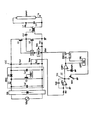
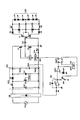
- the lighting circuit according to the first embodiment of the present invention includes a rectifier circuit DB that rectifies the commercial power supply Vin, and a power factor correction circuit PFC that boosts and smoothes the output of the rectifier circuit DB.
- the power factor correction circuit PFC is a well-known boost chopper circuit.
- the power factor correction circuit PFC includes a small-capacitance capacitor Cs2 connected in parallel to the rectification output terminal of the rectification circuit DB, a series circuit of an inductor L1 and a switching element Q3 connected to the rectification output terminal of the rectification circuit DB, and a switching element.
- a smoothing electrolytic capacitor Cs1 connected in parallel to both ends of Q3 via a diode D1 and a chopper control unit CTR1 for on / off-controlling the switching element Q3 at a high frequency are included.
- the switching element Q3 is turned on / off at a frequency higher than the commercial frequency, so that the pause period of the input current from the commercial power source Vin is reduced and the input power factor is improved.
- the smoothing electrolytic capacitor Cs1 is charged with the boosted DC voltage. Since the charging energy to the capacitor Cs1 is insufficient in the valley portion of the commercial power supply Vin, a ripple voltage having a frequency component twice that of the commercial power supply Vin is superimposed on the output voltage VDC of the power factor correction circuit PFC. For example, when the input voltage and the frequency of the commercial power supply Vin are 100 V and 50 Hz, respectively, a ripple voltage of 100 Hz is superimposed on the output voltage VDC. Since other operations of the power factor correction circuit PFC are well known, a detailed description thereof will be omitted.
- the output voltage VDC of the power factor correction circuit PFC is a half-bridge inverter circuit comprising a series circuit of switching elements Q1 and Q2, a driving circuit DRV thereof, a capacitor Cd1, an insulating transformer T1, a resonant inductor Lr1 and a resonant capacitor Cr1.
- an inverter circuit A resistor Rs1 for detecting an input current is inserted into the input terminal on the low voltage side of the inverter circuit.
- the inverter circuit converts the DC voltage VDC into a high-frequency voltage and supplies power to the fluorescent lamp Lamp1.
- the switching elements Q1 and Q2 are constituted by, for example, MOSFETs incorporating reverse diodes connected in parallel between the source and drain.
- the switching elements Q1 and Q2 are alternately turned on / off at high frequency, the switching element Q1 is on, and the switching element Q2 is off, the positive electrode of the DC power supply VDC ⁇ the switching element Q1 ⁇ the capacitor Cd1 ⁇ the primary of the insulation transformer T1.
- a current flows through the negative path of winding ⁇ current detection resistor Rs1 ⁇ DC voltage VDC to charge capacitor Cd1.
- the switching element Q1 When the switching element Q1 is off and the switching element Q2 is on, a current flows through the path of the capacitor Cd1, the switching element Q2, the primary winding of the insulating transformer T1, and the capacitor Cd1, and the capacitor Cd1 is discharged. Therefore, the insulating transformer T1 is excited by the high frequency voltage, and a boosted high frequency voltage is generated in the secondary winding.
- the boosted high frequency voltage is applied to a series resonance circuit of the resonance inductor Lr1 and the resonance capacitor Cr1, and further boosted by a resonance action. Further, a high frequency high voltage is generated at both ends of the resonance capacitor Cr1, and this high voltage is applied to both ends of the discharge lamp Lamp1.
- the discharge lamp Lamp1 is a cold cathode fluorescent lamp (CCFL), a hot cathode fluorescent lamp (HCFL), or the like.
- the oscillation frequency of the switching elements Q1, Q2 is normally set to a frequency higher than the resonance frequency.
- the oscillation frequency increases, the light output of the discharge lamp Lamp1 decreases.
- the oscillation frequency decreases, the light output of the discharge lamp Lamp1 increases.
- the lighting period and the extinguishing period are repeated at a low frequency (for example, 120 Hz) synchronized with the video update period of the liquid crystal display device.
- the switching elements Q1 and Q2 may be alternately turned on and off at a high frequency sufficiently higher than the resonance frequency even during the extinguishing period. In this case, the operating frequency of on / off is switched to a frequency that is high enough that the lighting of the discharge lamp Lamp1 cannot be maintained.
- the inverter circuit includes a pulse width modulation controller PWM1.
- a feedback control circuit is added to the inverter circuit. In this feedback control, by inputting the detection signal from the resistor Rs1, the on-time and the operating frequency of the switching elements Q1, Q2 are adjusted so that the input current to the inverter circuit becomes a predetermined value. Further, this feedback control functions only during the lighting period when the enable signal EN1 is High, and the oscillation of the inverter circuit is stopped during the extinguishing period when the enable signal EN1 is Low.
- the drive circuit DRV receives a high frequency output from the pulse width modulation controller PWM1, and applies a high frequency pulse voltage between the gate electrode of the switching element Q2 and the gate and source electrodes of the switching element Q1.
- these high-frequency phases are opposite to each other. Therefore, by applying these high frequency pulses, the switching element Q2 is turned on / off at a high frequency, and conversely, the switching element Q1 is turned off / on at a high frequency.
- the ON times of the switching elements Q1, Q2 are set equally.
- the oscillation frequency is constant and the on-time of each switching element Q1, Q2 increases or decreases.
- the feedback control is control of the oscillation frequency, the operating frequency at which the switching elements Q1 and Q2 are alternately turned on changes.
- the output is decreased by shortening the ON time of the switching elements Q1 and Q2 or increasing the operating frequency. As the output increases or decreases, the input current becomes constant.
- the lighting period in which the enable signal EN1 is High and the light-off period in which the Enable signal EN1 is Low are repeated at a low frequency (for example, 120 Hz) synchronized with the video update cycle of the liquid crystal display device.
- the light output is adjusted by changing the time ratio between the lighting period and the extinguishing period.
- the enable signal EN1 is output from the feedforward control circuit FF.
- the feedforward control circuit FF includes resistors Ra1, Ra2, Ri1, an integration capacitor Ca2, a reset switch SW1 of the integration capacitor Ca2, an operational amplifier OP1, a comparator CMP1, and a reference voltage Vref1.
- Resistors Ra1 and Ra2 output a divided voltage signal Vsns of voltage VDC.
- This voltage division signal Vsns may be used as a signal for output voltage control by the power factor correction circuit PFC (that is, an input voltage to the chopper control circuit CTR1).
- the divided voltage signal Vsns is input to an integrating circuit including an operational amplifier OP1 and a capacitor Ca2 via a resistor Ri1.
- the output Vint of the integration circuit is input to the negative input terminal of the comparator CMP1.
- the reference voltage Vref1 is input to the positive input terminal of the comparator CMP1.
- the output of the comparator CMP1 is input to the reset input R of the flip-flop circuit RSFF1.
- the ON pulse signal of the dimming signal generator DIM is input to the set input S of the flip-flop circuit RSFF1.
- the inverted output Q ′ of the flip-flop circuit RSFF1 is output to the reset switch SW1.
- the enable signal EN1 which is the non-inverted output Q of the flip-flop circuit RSFF1, is output to the pulse width modulation controller PWM1.
- the pulse width modulation controller PWM1 turns on / off the switching operation of the inverter circuit based on the enable signal EN1.
- This integrating circuit integrates the voltage Vsns obtained by dividing the output voltage VDC of the power factor correction circuit PFC by the resistors Ra1 and Ra2, and outputs the integrated voltage Vint.
- the integration time constant is determined by the capacitance of the input resistor Ri1 and the capacitor Ca2 that is the feedback impedance.
- the operational amplifier OP1 is a differential amplifier with extremely high input impedance and amplification factor, and its + side input terminal and ⁇ side input terminal are at the same potential, that is, in a virtual short circuit (imaginary short) state. Since the + side input terminal of the operational amplifier OP1 is connected to the ground potential, the potential of the ⁇ side input terminal is fixed to the ground potential.
- the switch SW1 resets the integrating capacitor Ca2.
- the potentials at both ends of the capacitor Ca2 are both ground potentials, so the residual charge of the capacitor Ca2 is zero and the integrated voltage Vint is 0 volts.
- the switch SW1 is turned OFF in order to start integration, a current flows through the capacitor Ca2 via the resistor Ri1 due to the voltage Vsns obtained by dividing the output voltage VDC of the power factor correction circuit PFC by the resistors Ra1 and Ra2, and the capacitor Ca2 is charged. Since the input impedance of the operational amplifier OP1 is extremely high, the current flowing through the resistor Ri1 flows only through the capacitor Ca2.
- the charging current at this time is a constant current determined by (the voltage Vsns across the resistor Ri1) / (the resistance value of the resistor Ri1), the integrated voltage Vint decreases linearly.
- Both the operational amplifier OP1 and the comparator CMP1 are composed of operational amplifiers using two positive and negative power supplies. Therefore, in the comparator CMP1, when the integrated voltage Vint falls below the reference voltage Vref1 in a negative potential region lower than the ground potential, the output of the comparator CMP1 becomes High.
- Figure 2 shows the operation timing of each part.
- the output voltage VDC of the power factor correction circuit PFC the ON pulse signal of the dimming signal generator DIM, the OFF pulse signal of the dimming signal generator DIM, and the voltage Vint of the integration capacitor Ca2 are compared from above.
- An enable signal EN1 which is an output of the device CMP1 and an output of the flip-flop circuit RSFF1 is shown.
- the output voltage VDC of the power factor correction circuit PFC includes a so-called ripple voltage whose voltage fluctuates periodically as shown in FIG.
- This ripple voltage fluctuates the power supplied to a load circuit such as a lamp.
- the ripple voltage can be reduced by increasing the capacitance of the smoothing capacitor Cs1 in the power factor correction circuit PFC.
- the inverter circuit performs control to correct the ripple voltage. That is, when the DC voltage VDC which is the output voltage of the power factor correction circuit PFC is high, the feedforward control circuit corrects the inverter output to be small. On the other hand, when the DC voltage VDC is low, the inverter output is corrected to be increased.
- increase / decrease in light output is controlled by lighting time.
- the enable signal EN1 output from the non-inverted output Q of the flip-flop circuit RSFF1 Becomes High.
- the pulse width modulation controller PWM1 performs control for lighting the lamp.
- the inverted output Q ′ of the flip-flop circuit RSFF1 becomes Low.
- the reset switch SW1 is turned off.
- the integration operation to the capacitor Ca2 of the integration circuit is started.
- the DC voltage VDC is integrated.
- the capacitor Ca2 is charged slowly when the DC voltage VDC is low and quickly when the DC voltage VDC is high.
- the output of the comparator CMP1 is input to the reset terminal of the flip-flop circuit RSFF1. Therefore, when the output of the comparator CMP1 becomes High, the enable signal EN1 that is the non-inverted output Q of the flip-flop circuit RSFF1 becomes Low. When the enable signal EN1 becomes Low, the pulse width modulation controller PWM1 performs control to turn off the lamp.
- an OFF pulse signal is output from the dimming signal generator DIM and input to the reset terminal of the flip-flop circuit RSFF1.
- the ON pulse signal is output again from the dimming signal generator DIM and input to the set terminal of the flip-flop circuit RSFF1. Thereafter, the same operation is repeated.
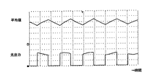
- FIG. 3 is a graph showing an example of the operation of this embodiment.
- the figure shows a light output waveform when the lamp Lamp1 is turned on and off with a DC power source including a ripple voltage of 100 Hz and a waveform obtained by averaging the waveform. From the optical output waveform, it can be seen that lighting and extinguishing are repeated periodically, and the peak value varies depending on the ripple voltage. On the other hand, looking at the averaged optical output waveform, it can be seen that the peak values are aligned. That is, when the direct current voltage is high, the lighting time is shortened, and when the direct current voltage is low, the lighting time is lengthened. Therefore, the amount of light per pulse emission is constant. As a result, the average value of the light output can be made constant, and flicker can be reduced.
- the light output is constant by controlling the time ratio between lighting and extinguishing.
- the same effect can be obtained by controlling the time ratio between lighting and dimming lighting. Therefore, if a discharge lamp maintains a discharge in a dimming lighting state, lighting such as an LED or EL is possible.
- the switching elements Q1 and Q2 are alternately turned on / off at the first oscillation frequency (frequency relatively close to the resonance frequency).
- the switching elements Q1 and Q2 are alternately turned on / off at a second oscillation frequency higher than the first oscillation frequency (a frequency far from the resonance frequency but not extinguished). Therefore, bright and dark lighting can be obtained by alternately switching between these lighting periods and dimming lighting periods.
- the lighting period and the dimming lighting period are repeated at a low frequency (for example, 120 Hz) synchronized with the video update period of the liquid crystal display device.
- the average value of the turn-off time is more preferably 5% or more than 0% of the blinking period (for example, the time from t1 to t5 in FIG. 2).
- the time ratio of the lighting period (ON state period) in the lighting circuit is smaller than 100% and not more than 95% with respect to the total of the lighting period and the extinguishing period (OFF state period).
- the ripple voltage is often about ⁇ 5% of the DC voltage VDC, and such fluctuation can be corrected by an increase / decrease in lighting time of ⁇ 5%.
- the reference voltage Vref1 is preferably set in a range in which the average value of the turn-off time is 5% or more of the blinking cycle. That is, the reference voltage Vref1 is preferably set so that the dimming range is 0% to 95% of the blinking cycle. The most suitable time ratio is around 95%.
- the present invention is effective when it repeatedly blinks at a low frequency.
- the image update period of a general video display device is 30 Hz or more, but the present invention is effective when the flashing lighting is from about 30 Hz to about 1 kHz.
- the ripple frequency is 100 Hz and the blinking frequency is 120 Hz.
- light fluctuation of about 5% appears at a frequency difference of 20 Hz due to interference between the ripple frequency and the blinking frequency.
- the flickering tendency tends to decrease in inverse proportion. Therefore, if the blinking frequency is increased to about 10 times the ripple frequency, the flickering feeling is reduced to about 1/10. Therefore, if the ripple voltage is about 5%, the flickering is reduced to a negligible level.
- the higher the blinking frequency the smaller the light output and the more difficult it is to obtain a clear image.
- the lighting time is corrected by detecting the input voltage of the lighting circuit.
- the lighting time may be corrected by detecting the input voltage of the smoothing circuit instead of the input voltage of the lighting circuit. The same applies to the following embodiments.
- FIG. 4 shows a lighting circuit according to a second embodiment of the present invention.
- the lighting time is determined from the integrated value of the input power.
- the detection signal Vsns of the DC voltage VDC and the detection signal Isns of the input current of the inverter circuit are input to the multiplier MUL1, and as a result, the power detection signal Wsns is output.
- the power detection signal Wsns is input to an integration circuit including an operational amplifier OP1 and an integration capacitor Ca2.
- the integral value Vint becomes equal to or less than the reference value Wref1
- the comparator CMP1 outputs High, and the inverter circuit is turned off.
- the high frequency oscillator OSC1 oscillates at a high frequency whose frequency is the operating frequency of the inverter circuit. This oscillation is controlled by the enable signal EN1, and the high frequency oscillator OSC1 oscillates when the enable signal EN1 is High and stops oscillating when it is Low. Alternatively, the high frequency oscillator OSC1 oscillates at the first oscillation frequency (a frequency relatively close to the resonance frequency) when the enable signal EN1 is High, and is higher than the first oscillation frequency when the enable signal EN1 is Low. Oscillates at an oscillation frequency of 2 (a frequency far from the resonance frequency but not extinguished).
- the lighting time is controlled so that the integral value of the input power of the inverter circuit becomes a predetermined power amount for each lighting period, the light output per lighting period can be controlled to be constant. . Therefore, it is possible to reduce flicker due to the ripple voltage of the DC voltage.
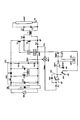
- FIG. 5 shows a lighting circuit according to a third embodiment of the present invention.
- a current detection circuit DET2 that detects the lamp current ila is inserted between one end of the inverter circuit output and the lamp Lamp1.
- a feedback control circuit FBC2 for setting a reference voltage (corresponding to Vref1 in FIG. 1) of the feedforward control circuit so that the output of the current detection circuit DET2 becomes a predetermined value, and an output signal of the feedback control circuit FBC2 on the primary side
- a lamp current feedback circuit is provided that includes a photocoupler PC1 that transmits to the photocoupler and a low-pass filter LPF1 that smoothes the output of the photocoupler PC1.
- the inverter circuit includes the high-frequency oscillator OSC1 described in the second embodiment. Other configurations are the same as those of the first embodiment.
- feedback control is suppressed for long-term load fluctuations, which are difficult to control by feedforward.
- feedforward control a control response is shown only for a certain input, so that it is difficult to design a sufficient control for various disturbances. Therefore, it is effective to use feedback control together with the load current fluctuation factors other than the power supply ripple.
- the current detection circuit DET2 detects the lamp current ila.
- the feedback control circuit FBC2 controls the positive input terminal voltage of the comparator CMP1, which is the target value of the feedforward control, via the photocoupler PC1 and the smoothing low-pass filter LPF1.
- the response speed of this feedback control is set sufficiently slow so as not to respond at the power supply frequency or the blinking frequency. With such a setting, it is possible to accurately perform correction control of load current fluctuation due to ambient temperature change, output change due to long-term use, and the like.
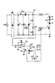
- FIG. 6 shows a lighting circuit according to a fourth embodiment of the present invention.
- the present embodiment is a circuit for lighting an LED.
- the lighting circuit includes a rectifier circuit DB and a power factor correction circuit PFC.
- the output voltage VDC of the power factor correction circuit PFC is supplied to an LED lighting circuit comprising a plurality of LEDs connected in series with the current limiting circuit CRG and a switch Q2.
- the current limiting circuit CRG is a circuit that controls the current flowing through the LED to be stable, and is a resistor, a step-down chopper circuit, a constant current element, or the like, for example.
- the switch Q2 of the LED lighting circuit is turned on / off by the drive circuit DRV.
- the switch Q2 is turned on when the enable signal EN1 is High, and the switch Q2 is turned off when the enable signal EN1 is Low.
- the resistor Ra1, Ra2, Ri1, the integration capacitor Ca2, the integration capacitor reset switch SW1, the operational amplifier OP1, the comparator CMP1, and the reference voltage Vref1 are included.
- a feedforward control circuit is provided.
- the reference voltage Vref1 is input to the positive input terminal of the comparator CMP1.
- the output of the comparator CMP1 is input to the reset input R of the flip-flop circuit RSFF1.
- the ON pulse signal of the dimming signal generator DIM is input to the set input S of the flip-flop circuit RSFF1.
- the inverted output Q ′ of the flip-flop circuit RSFF1 is output to the reset switch SW1.
- the drive circuit DRV controls the turning on / off of the LED.
- the dimming signal generator DIM periodically outputs an ON pulse signal and an OFF pulse signal.
- flicker due to ripple voltage is reduced when an LED is used as an element that is lit by a DC power source. Since the LED is lit by the smoothing circuit output, it does not require a circuit for converting to a high frequency unlike the inverter circuit. However, as described above, flickering occurs at a low frequency when blinking is performed.
- the feedforward control for controlling the lighting time is performed so that the lighting light amount per time does not change, it is possible to reduce the flicker caused by the ripple voltage caused by the power source.
- the constant voltage converter circuit for removing the power supply ripple is not necessary, the loss of the lighting circuit can be reduced.
- FIG. 7 shows a lighting circuit according to a fifth embodiment of the present invention.
- the LED is lit while performing insulation between the power supply side and the load side.
- the lighting circuit includes a rectifier circuit DB that rectifies commercial power and a power factor correction circuit PFC that boosts and smoothes the output of the rectifier circuit DB.
- the output voltage VDC of the power factor correction circuit PFC includes switching elements Q1 and Q2, a driving circuit DRV thereof, a capacitor Cd1, an insulating transformer T1, diodes D2 to D5, smoothing capacitors Cs3 and Cs4, and smoothing inductors Ls1 and Ls2. Supplied to the half-bridge circuit.
- a resistor Rs1 for detecting an input current is inserted into the input terminal on the low voltage side of the half bridge circuit.
- the DC voltage VDC is converted into an insulated DC voltage by the half bridge circuit, and power is supplied to the LED.
- the half bridge circuit includes a pulse width modulation controller PWM1.
- a feedback control circuit is blown to the half bridge circuit. In this feedback control, by inputting the detection signal from the resistor Rs1, the on-time and the operating frequency of the switching elements Q1 and Q2 are adjusted so that the input current of the half bridge circuit becomes a predetermined value.
- this embodiment also includes a feed consisting of resistors Ra1, Ra2, Ri1, an integration capacitor Ca2, an integration capacitor reset switch SW1, an operational amplifier OP1, a comparator CMP1, and a reference voltage Vref1.
- a forward control circuit is provided.
- the reference voltage Vref1 is input to the positive input terminal of the comparator CMP1.
- the output of the comparator CMP1 is input to the reset input R of the flip-flop circuit RSFF1.
- the ON pulse signal of the dimming signal generator DIM is input to the set input S of the flip-flop circuit RSFF1.
- the inverted output Q ′ of the flip-flop circuit RSFF1 is output to the reset switch SW1.
- the half-bridge circuit controls the turning on / off of the LED.
- the dimming signal generator DIM periodically outputs an ON pulse signal and an OFF pulse signal.
- This embodiment is an example of reducing flicker due to ripple voltage while performing electrical insulation between the power supply side and the load side when an LED is used as the lighting element.
- FIG. 8 shows a lighting circuit according to a sixth embodiment of the present invention.
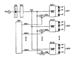
- the LEDs are sequentially turned on in a plurality of groups.
- the lighting circuit includes a rectifier circuit DB that rectifies the commercial power supply Vin and a power factor correction circuit PFC that boosts and smoothes the output of the rectifier circuit DB.
- the output voltage VDC of the power factor correction circuit PFC is supplied to the insulation converters DCC1 to DCC8.
- LEDs 1 to LED8 are connected to the outputs of the insulating converters DCC1 to DCC8, respectively.
- the lighting circuit includes feedforward control circuits FF1 to FF8.
- the dimming signal generator DIM generates a plurality of on / off timing signals DIM-1 to DIM-8.
- the feedforward control circuits FF1 to FF8 output enable signals EN1 to EN8 for determining the lighting time of each LED to the isolation converters DCC1 to DCC8 based on the timing signals DIM-1 to DIM-8 of the dimming signal generator DIM. To do.
- the insulating converters DCC1 to DCC8 are repeatedly turned on / off in response to the enable signals EN1 to EN8.
- FIG. 9 shows an arrangement example of each LED. As shown in the figure, the LEDs 1 to 8 are grouped for each row and controlled to be lit.
- Fig. 10 shows the operation timing of each signal.
- the figure shows the output voltage VDC of the power factor correction circuit PFC, the outputs DIM-1, DIM-2, DIM-8 of the dimming signal generator DIM, and the enable signals EN1, EN2, EN8 of the feedforward control circuit. .
- the dimming signal generator DIM starts lighting sequentially from the LED 1 and outputs a timing signal for periodically blinking and lighting.
- the feedforward control circuits FF1 to FF8 determine the lighting time according to the input of the DC voltage VDC, and send the enable signals EN1 to EN8 to the respective isolated converters DCC1 to DCC8. Output.
- the lighting is performed sequentially in this way, the image quality of the moving image display of the liquid crystal display device can be improved. Further, flicker due to the ripple voltage superimposed on the DC power supply can be reduced. Further, a converter for stabilizing the DC voltage VDC is not required, and power can be supplied to the LEDs with high efficiency.
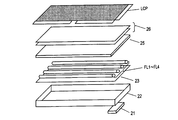
- FIG. 11 is an exploded perspective view showing a schematic configuration of a liquid crystal display device using the lighting device according to the first to third embodiments.
- a backlight is disposed on the back surface (directly below) of the liquid crystal panel LCP, and the backlight is disposed above the casing 22, the reflector 23 and a plurality of fluorescent lamps FL1 to FL4 disposed thereon.
- a diffusing plate 25 and an optical sheet 26 such as a prism sheet.
- an inverter substrate 21 for lighting the fluorescent lamps FL1 to FL4 is installed on the rear surface of the housing 22.
- the reflector 23 effectively directs the irradiation light of each of the fluorescent lamps FL1 to FL4 to the front surface.
- the diffusion plate 25 has a function of diffusing the light from the fluorescent lamps FL1 to FL4 and the reflection plate 23 and averaging the brightness distribution of the illumination light to the front surface.
Landscapes
- Circuit Arrangements For Discharge Lamps (AREA)
- Circuit Arrangement For Electric Light Sources In General (AREA)
Abstract
点灯装置であって、点灯回路と、調光信号回路RSFF1と、フィードフォワード制御回路FFとを備える。点灯回路は、商用電源Vinを整流・平滑した出力VDCを入力して光源Lamp1に電力を供給する。調光信号回路RSFF1は、前記点灯回路の出力を周期的にオン状態とオフ状態(または減光状態)に切り替えるタイミング信号を点灯回路に与える。フィードフォワード制御回路FFは、前記点灯回路の入力電圧または平滑回路の入力電圧を検知して前記光源の光出力を所望の値となるように点灯時間を補正する制御信号を前記調光信号回路に送出する。
Description
本発明は液晶表示装置のバックライト装置などに用いられる点灯装置に関し、特に光のちらつきの低減と回路効率の改善に関する。
液晶表示装置は、一般的に、冷陰極ランプなど蛍光ランプを複数点灯させたバックライト装置の光を用いて画像表示を行っている。蛍光ランプの点灯回路にはインバータ回路が一般的に用いられる。高周波でランプを点灯させることによりランプ発光効率が向上し、トランスなど電子部品の小型化が可能となっている。
液晶表示装置は、その普及に伴って、更なる機器の高効率化が求められている。特に、バックライト装置は液晶表示装置の大部分の電力を消費するため、その高効率化は重要な課題である。この要請に応えるため、ゼロ電圧スイッチングなどのソフトスイッチング手法を放電灯点灯回路に採用することで、インバータ回路のスイッチング損失を低減することが提案されている。インバータ回路に入力する直流電源を高電圧仕様にして、昇圧トランスの損失を低減することも提案されている。
また、液晶表示装置の光源として、蛍光ランプだけでなく、半導体発光であるLEDや有機ELなどが実用化されつつある。従って、これらの発光デバイスに電力供給する点灯回路に対しても高効率化が求められている。
しかしながら、これらのバックライト装置の点灯回路における電力変換の効率は、一般照明用の点灯回路のそれよりも低い。その理由は、一般照明用の点灯回路よりもちらつきを抑えるための直流安定化回路を別途必要とするからである。
ここで一般照明用の点灯回路でちらつきが問題とならない理由を説明する。たとえば、商用電源(50Hz)を電源とした蛍光灯インバータ回路のちらつきについて考える。蛍光灯インバータ回路では、商用電源を整流回路で整流し、平滑回路で直流電圧を平滑してインバータ回路に直流電力を供給し、インバータ回路がランプに高周波電力を供給している。平滑回路の出力電圧は、完全な直流電圧とはなっておらず、所謂リップル電圧を含んでいる。
そのため、インバータ回路の出力電圧もリップル電圧により多少変動する。たとえばインバータ回路に入力された直流電圧に100Hzのリップル電圧が含まれているとする。この100Hzは、商用電源を全波整流したときに現れる周波数成分である。このリップル電圧を除去せずにインバータ回路がランプを点灯させると、光出力に100Hzの周波数成分をもつ変動が生じる。一般照明用のインバータ回路のリップル電圧のレベルはおよそ10%以下である。この光を直視しても、ちらつきはほとんど感じない。これは光変化の周波数が100Hzと高いからである。そのため、一般照明などで用いる蛍光灯のインバータ回路などではこのちらつきは特に問題とならない。
ところが液晶表示装置においては、一般照明と異なる点灯方法を用いているため、ちらつきが顕著となる。なぜなら、一般的な液晶表示装置のバックライト装置は、比較的低周波でインパルス点灯を行っているからである。
特許文献1(特開平7-272889号公報)では、蛍光ランプに高周波電圧を印加する期間と印加しない期間を周期的に繰り返すことで、蛍光ランプの調光を行っている。この調光では、光出力が点灯と消灯の時間比率から求まる。従って、ランプ電流を連続的に可変する方式に比べて、光出力が直線的に変化する。また、点滅することで液晶表示装置の動画ボケを改善している。
特許文献2(特開平11-202286号公報)は、液晶表示装置において、光源をインパルス発光させることで鮮明な画像を得る技術を開示している。この技術によれば、光源を画像の更新周期に合わせて発光させることで、液晶表示装置の欠点である応答性が改善する。つまり、表示画像を60Hzで更新する場合、光源も60Hzでインパルス発光させれば良い。このように光源をインパルス発光させるのは液晶表示装置にとって有用である。
しかし、このインパルス発光のためには安定した電源が必要となる。なぜなら、光源の電源に商用電源のリップル電圧が含まれていると、リップル電圧の周波数とインパルス発光の周波数の干渉によるゆらぎが発生するからである。たとえば商用電源の周波数が50Hzで、平滑回路出力に100Hzのリップル電圧が生じているとする。このときインパルス発光の周波数を120Hzとすると、20Hzの光変動を生じる。すなわち、商用電源の周波数とインパルス発光の周波数の差が低周波になると、それがちらつきとして現れる。
このちらつきの対策として、インパルス発光の周波数をリップル周波数から遠ざける方法がある。つまり商用電源の周波数とインパルス発光の周波数の差が大きくなるように設定する。リップル周波数を100Hz、インパルス発光周波数を380Hzにそれぞれ設定した場合、周波数差は280Hzとなるので、ちらつきは目立たなくなる。
しかし、特許文献2のように鮮明な画像を効率的に得るには、インパルス発光の周期を表示画像の更新周期に同期させる必要がある。すなわち、液晶表示更新を60Hzで行う場合は、インパルス発光の周波数は60Hz、120Hz、180Hzから選択できる。この場合、もっとも画面が明るく、かつ鮮明な画像を得るにはなるべく低い周波数を選択しなくてはならない。
そこで一般的な液晶表示装置は、商用電源に起因する直流電源のリップル電圧を除去する安定化電源回路を備えている。リップルの影響がないのであれば、そのちらつきの問題は発生しない。しかし、電源安定化によって回路損失が生じるため、液晶表示装置の電力から光への変換効率が低下する。
ところで、電源安定化回路を用いずにリップルの影響を低減する方法としてインバータ回路に電源リップル除去機能を付加することが考えられる。たとえばランプ電流をフィードバック制御すればよい。フィードバック制御を行えばランプ電流は略一定となり、リップル電圧による光出力の変動を除去できる。
しかし、このフィードバック制御では、ランプ電流を絶縁された2次側回路で検出し、この検出信号を非絶縁である1次側スイッチング回路ヘ伝達する必要がある。従って、実際には、その伝達回路を含めたフィードバック制御の設計は困難である。
もうひとつの手法として、フィードフォワード制御を行うことが考えられる。リップル電圧に応じてインバータ出力を増減させれば、制御回路は非絶縁の1次側で構成することができ、絶縁回路の設計は容易である。また、リップル電圧は比較的安定に発生するので、フィードフォワード制御には適している。この放電灯点灯装置のフィードフォワード制御についても様々な手法が提案されている。
特許文献3(特開2002-330591号公報)では、インバータの入力電圧を検知し、電圧変動によるランプ電流変化を抑制するように、スイッチの駆動周波数またはスイッチオン・スイッチオフの時間比を変化させる技術が提案されている。
また、特許文献4(特表2007-529872号公報)では、インダクタなどにエネルギーを蓄積して、光源にエネルギーを与えるコンバータにおいて、蓄積エネルギーが一定となるように、フィードフォワード制御する技術が提案されている。
特許文献3は連続点灯に適した技術である。しかしながら、液晶表示装置で用いられるランプの点灯制御(バースト調光制御)のように点滅を繰り返す調光においては、とくに蛍光灯などを点滅させた場合に、ランプの始動タイミングのずれなどでちらつきが発生する問題がある。
特許文献4は、LEDなどの発光素子へのエネルギーを一旦インダクタなどに蓄積し、その後、発光素子を発光させる。従って、蓄積のためのエネルギー損失を伴う。また、エネルギー蓄積のための素子を小さくするために、スイッチング周波数を高める必要があり、これによりスイッチング損失も増加する傾向にある。
本発明は、このような従来技術の課題を解決すべくなされたものであり、液晶表示装置の光源を点灯させるインバータ回路で電源変動に起因するちらつきを除去する制御を確実に行うことにより、液晶表示装置の画像表示性能を損なわずに安価で高効率な点灯装置を提供することを目的とする。
本発明の態様は点灯装置であって、商用電源を整流する整流器と、前記整流器の出力を平滑する少なくとも1つの平滑回路と、前記平滑回路の出力を入力して光源に電力を供給する点灯回路と、前記点灯回路の出力を周期的にオン状態と、オフ状態または減光状態に切り替えるタイミング信号を前記点灯回路に与える調光信号回路と、前記点灯回路の入力電圧または前記平滑回路の入力電圧を検知して前記光源の光出力を所望の値となるように点灯時間を補正する制御信号を前記調光信号回路に送出するフィードフォワード制御回路とを備える。
前記点灯回路は入力電流を一定にする制御回路を有してもよい。
前記フィードフォワード制御回路は、前記点灯回路の出力がオンとなると同時に前記点灯回路の入力電圧または平滑回路の入力電圧に比例する電圧信号の積分を開始するのが好ましい。さらに、前記フィードフォワード制御回路は、前記電圧信号の積分値が所定の値になると前記調光信号回路に前記点灯回路をオフさせる信号を送出するのが好ましい。
前記フィードフォワード制御回路は、前記点灯回路の出力がオンとなると同時に前記点灯回路の入力電圧信号と入力電流信号の乗算値の積分を開始するのが好ましい。さらに、前記フィードフォワード制御回路は、前記積分の値が所定の値になると、前記調光信号回路に前記点灯回路をオフさせる信号を送出するのが好ましい。
前記調光信号回路は、前記点灯回路のオン状態期間を、時間比率100%よりも小さくすることが好ましい。
前記調光信号回路の周波数は、30Hzから1000Hzであってもよい。
前記光源は、半導体光源であってもよい。
本発明の態様は、上記点灯装置を備えたバックライト装置でもよい。
本発明によれば、光源の発光量が所望の値となるように点灯時間を調整するフィードフォワード制御が実行される。点灯と消灯の時間比率を可変して光量補正することができるので、高速なフィードバック制御などが不要となる。従って、安価な構成で、電源リップルによるちらつきを抑制できる。
以下図面を参照しながら、本発明の実施形態を説明する。
(第1実施形態)
図1に示すように、本発明の第1実施形態に係る点灯回路は、商用電源Vinを整流する整流回路DBと、その出力を昇圧して平滑する力率改善回路PFCを有する。
図1に示すように、本発明の第1実施形態に係る点灯回路は、商用電源Vinを整流する整流回路DBと、その出力を昇圧して平滑する力率改善回路PFCを有する。
力率改善回路PFCは周知の昇圧チョッパ回路である。力率改善回路PFCは、整流回路DBの整流出力端に並列接続された小容量のコンデンサCs2と、整流回路DBの整流出力端に接続されたインダクタL1とスイッチング素子Q3の直列回路と、スイッチング素子Q3の両端にダイオードD1を介して並列接続された平滑用の電解コンデンサCs1と、スイッチング素子Q3を高周波でオン・オフ制御するチョッパ制御部CTR1を含む。力率改善回路PFCでは、スイッチング素子Q3が商用周波数よりも高周波でオン・オフされることで、商用電源Vinからの入力電流の休止期間が少なくなり、入力力率が改善される。平滑用の電解コンデンサCs1には昇圧された直流電圧が充電される。商用電源Vinの谷部ではコンデンサCs1への充電エネルギーが不足するので、力率改善回路PFCの出力電圧VDCには、商用電源Vinの2倍の周波数成分のリップル電圧が重畳する。例えば、商用電源Vinの入力電圧およびその周波数がそれぞれ、100V、50Hzである場合には、100Hzのリップル電圧が出力電圧VDCに重畳される。力率改善回路PFCのその他の動作については周知であるので、その詳細な説明は省略する。
力率改善回路PFCの出力電圧VDCは、スイッチング素子Q1、Q2の直列回路と、その駆動回路DRVと、キャパシタCd1と絶縁トランスT1と、共振インダクタLr1と共振キャパシタCr1とからなるハーフブリッジインバータ回路(以下、単にインバータ回路と称する)に供給される。インバータ回路の低電圧側の入力端子には入力電流を検出する抵抗Rs1が挿入されている。インバータ回路は直流電圧VDCを高周波電圧に変換し、蛍光ランプLamp1に電力を供給する。
スイッチング素子Q1,Q2は、例えば、ソース‐ドレイン間に並列接続される逆方向ダイオードを内蔵するMOSFETで構成される。スイッチング素子Q1,Q2は高周波で交互にオン・オフされ、スイッチング素子Q1がオンで、スイッチング素子Q2がオフのときは、直流電源VDCの正極→スイッチング素子Q1→キャパシタCd1→絶縁トランスT1の1次巻線→電流検出抵抗Rs1→直流電圧VDCの負極の経路で電流が流れてキャパシタCd1が充電される。スイッチング素子Q1がオフで、スイッチング素子Q2がオンのときは、キャパシタCd1→スイッチング素子Q2→絶縁トランスT1の1次巻線→キャパシタCd1の経路で電流が流れてキャパシタCd1が放電される。したがって、絶縁トランスT1は高周波電圧により励磁され、その2次巻線には昇圧された高周波電圧が発生する。この昇圧された高周波電圧は、共振インダクタLr1と共振キャパシタCr1の直列共振回路に印加されて、共振作用により更に昇圧される。さらに、共振キャパシタCr1の両端には高周波の高電圧が発生し、この高電圧が放電ランプLamp1の両端に印加される。ここで、放電ランプLamp1は、冷陰極蛍光ランプ(CCFL)、熱陰極蛍光ランプ(HCFL)などである。
スイッチング素子Q1,Q2の発振周波数は、通常、共振周波数よりも高い周波数に設定される。この発振周波数が高くなると放電ランプLamp1の光出力が低下する。一方、発振周波数が低くなると放電ランプLamp1の光出力が増加する。本実施形態では、スイッチング素子Q1,Q2が高周波で交互にオン・オフする点灯期間と、スイッチング素子Q1,Q2が共にオフである消灯期間とがあり、放電ランプLamp1は、これら点灯期間と消灯期間とが交互に切り換わることで点滅点灯する。さらに、点灯期間と消灯期間は、液晶表示装置の映像更新周期に同期した低い周波数(例えば、120Hz)で繰り返される。なお、消灯期間でもスイッチング素子Q1,Q2を共振周波数よりも十分に高い高周波で交互にオン・オフさせてもよい。この場合、オン・オフの動作周波数は、放電ランプLamp1の点灯を維持できないほど高い周波数に切り替えられる。
インバータ回路はパルス幅変調制御器PWM1を備える。インバータ回路にはフィードバック制御回路が付加されている。このフィードバック制御では、抵抗Rs1からの検出信号を入力することで、インバータ回路への入力電流が所定の値となるようにスイッチング素子Q1,Q2のオン時間や動作周波数が調整される。さらに、このフィードバック制御は、イネーブル信号EN1がHighとなる点灯期間でのみ機能し、イネーブル信号EN1がLowとなる消灯期間ではインバータ回路の発振そのものが停止している。
駆動回路DRVは、パルス幅変調制御器PWM1からの高周波出力を受けて、スイッチング素子Q2のゲート電極と、スイッチング素子Q1のゲート・ソース電極間とに高周波のパルス電圧を印加する。ただし、これらの高周波の位相は互いに逆である。したがって、これらの高周波パルスの印加によって、スイッチング素子Q2は高周波でオン/オフし、逆に、スイッチング素子Q1は高周波でオフ/オンする。なお、本実施形態において、各スイッチング素子Q1,Q2のオン時間は均等に設定される。また、フィードバック制御がオン時間の制御である場合には、発振周波数が一定で各スイッチング素子Q1,Q2のオン時間が増減する。フィードバック制御が発振周波数の制御である場合には、スイッチング素子Q1,Q2が交互にオンする動作周波数が変化する。
以上の動作を下記にまとめる。イネーブル信号EN1がLowのときは、スイッチング素子Q1,Q2は共にオフであり、インバータ回路の発振が停止しているので、放電ランプLamp1は消灯する。イネーブル信号EN1がHighのときは、スイッチング素子Q1,Q2が高周波で交互にオンすることにより、インバータ回路が発振し、その発振出力により放電ランプLamp1が点灯する。インバータ回路への入力電流は、抵抗Rs1により検出される。入力電流が既定値よりも小さい場合は、スイッチング素子Q1,Q2のオン時間を伸ばすか動作周波数を下げることで出力を増加させる。入力電流が既定値よりも大きい場合は、スイッチング素子Q1,Q2のオン時間を短縮するか動作周波数を上げることで出力を減少させる。これら出力の増加または減少によって、入力電流が一定になる。イネーブル信号EN1がHighである点灯期間とLowである消灯期間は、液晶表示装置の映像更新周期に同期した低い周波数(例えば、120Hz)で繰り返される。光出力は、点灯期間と消灯期間の時間比率を可変にすることで調整される。
イネーブル信号EN1は、フィードフォワード制御回路FFから出力される。フィードフォワード制御回路FFは、抵抗Ra1,Ra2,Ri1と、積分キャパシタCa2と、積分キャパシタCa2のリセットスイッチSW1と、演算増幅器OP1と、比較器CMP1と、基準電圧Vref1とを備える。抵抗Ra1とRa2は、電圧VDCの分圧信号Vsnsを出力する。この分圧信号Vsnsは、力率改善回路PFCによる出力電圧制御のための信号(つまりチョッパ制御回路CTR1への入力電圧)として用いられてもよい。分圧信号Vsnsは、抵抗Ri1を介して演算増幅器OP1とキャパシタCa2からなる積分回路に入力される。
積分回路の出力Vintは、比較器CMP1の負の入力端子に入力される。比較器CMP1の正の入力端子には、基準電圧Vref1が入力される。比較器CMP1の出力は、フリップフロップ回路RSFF1のリセット入力Rへ入力される。フリップフロップ回路RSFF1のセット入力Sには調光信号発生器DIMのONパルス信号が入力される。
フリップフロップ回路RSFF1の反転出力Q’はリセットスイッチSW1へ出力される。フリップフロップ回路RSFF1の非反転出力Qであるイネーブル信号EN1はパルス幅変調制御器PWM1に出力される。パルス幅変調制御器PWM1は、イネーブル信号EN1に基づいて、インバータ回路のスイッチング動作をオン・オフする。
ここで、積分回路について説明する。この積分回路は、力率改善回路PFCの出力電圧VDCを抵抗Ra1,Ra2によって分圧して得られた電圧Vsnsを積分し、その積分電圧Vintを出力する。積分時定数は、入力抵抗Ri1と帰還インピーダンスであるコンデンサCa2の容量で決まる。演算増幅器OP1は入力インピーダンスならびに増幅率が極めて高い差動増幅器であり、その+側入力端子と-側入力端子は同一電位、つまり仮想短絡(イマジナリーショート)の状態にある。演算増幅器OP1の+側入力端子はグランド電位に接続されているので、-側入力端子の電位は、グランド電位に固定される。スイッチSW1は積分コンデンサCa2をリセットする。スイッチSW1がONのとき、コンデンサCa2の両端電位は共にグランド電位となるから、コンデンサCa2の残留電荷はゼロとなり、積分電圧Vintは0ボルトとなる。積分を開始するべく、スイッチSW1をOFFすると、力率改善回路PFCの出力電圧VDCを抵抗Ra1,Ra2の分圧から得られた電圧Vsnsによって、抵抗Ri1を介してコンデンサCa2に電流が流れ、コンデンサCa2が充電される。演算増幅器OP1の入力インピーダンスは極めて高いから、抵抗Ri1に流れる電流はコンデンサCa2にのみ流れる。このときの充電電流は、(抵抗Ri1の両端電圧Vsns)÷(抵抗Ri1の抵抗値)で決まる一定電流となるから、積分電圧Vintは直線的に低下して行く。なお、演算増幅器OP1も比較器CMP1も正負2電源を用いるオペアンプで構成される。従って、比較器CMP1において、積分電圧Vintがグランド電位よりも低い負電位の領域で基準電圧Vref1を下回ると、比較器CMP1の出力がHighになる。
図2に各部の動作のタイミングを示す。図には上から、力率改善回路PFCの出力電圧VDCと、調光信号発生器DIMのONパルス信号と、調光信号発生器DIMのOFFパルス信号と、積分キャパシタCa2の電圧Vintと、比較器CMP1の出力と、フリップフロップ回路RSFF1の出力であるイネーブル信号EN1が示されている。
力率改善回路PFCの出力電圧VDCは、図2のように周期的に電圧が変動する所謂リップル電圧を含む。このリップル電圧が、ランプ等の負荷回路に供給する電力を変動させる。リップル電圧は、力率改善回路PFC内の平滑キャパシタCs1の容量を大きくすれば小さく出来る。しかし、力率改善回路の原理上、リップル電圧をゼロにするのは困難である。
したがって、別途DC-DCコンバータなどを用いて電圧を安定化することが考えられる。しかし、DC-DCコンバータは電力損失を生じてしまう。そこで本実施形態では、インバータ回路がリップル電圧分を補正する制御を行う。すなわち、力率改善回路PFCの出力電圧である直流電圧VDCが高いときには、フィードフォワード制御回路によりインバータ出力を小さくするように補正する。一方、直流電圧VDCが低いときはインバータ出力を大きくするように補正する。
本実施形態では、光出力の増減が点灯時間によって制御される。
時間t1の時点で調光信号発生器DIMからONパルス信号が出力され、フリップフロップ回路RSFF1のセット端子に信号が入力されると、フリップフロップ回路RSFF1の非反転出力Qから出力されるイネーブル信号EN1はHighになる。イネーブル信号EN1がHighになるとパルス幅変調制御器PWM1はランプを点灯する制御を行う。
また、フリップフロップ回路RSFF1の反転出力Q’はLowとなる。反転出力Q’がLowになるとリセットスイッチSW1はOFFになる。リセットスイッチSW1がOFFになると、積分回路のキャパシタCa2への積分動作が開始される。積分回路では、直流電圧VDCが積分される。この積分動作において、キャパシタCa2は、直流電圧VDCが低いときはゆっくり、直流電圧VDCが高いときは早く充電される。
その後、時間t3の時点でキャパシタCa2の電圧Vintが基準電圧Vref1よりも低くなると、比較器CMP1の出力はHighになる。
比較器CMP1の出力は、フリップフロッブ回路RSFF1のリセット端子に入力される。したがって、比較器CMP1の出力がHighになると、フリップフロップ回路RSFF1の非反転出力Qであるイネーブル信号EN1はLowになる。イネーブル信号EN1がLowになるとパルス幅変調制御器PWM1はランプを消灯する制御を行う。
時間t4の時点で調光信号発生器DIMからOFFパルス信号が出力され、フリップフロップ回路RSFF1のリセット端子に入力される。
時間t5の時点で再び調光信号発生器DIMからONパルス信号が出力され、フリップフロップ回路RSFF1のセット端子に入力される。以下、同じ動作を繰り返す。
図3は本実施形態の動作の例を示したグラフである。図には、100Hzのリップル電圧を含む直流電源で、ランプLamp1を点滅点灯させたときの光出力波形と当該波形を平均化した波形が示されている。光出力波形から、周期的に点灯と消灯が繰り返され、そのピーク値がリップル電圧によって変化していることがわかる。一方、平均化された光出力波形を見ると、ピーク値が揃っていることがわかる。つまり、直流電圧が高いときには点灯時間を短くし、直流電圧が低いときには点灯時間を長くする制御が行われるので、パルス発光の1回あたりの光量が一定になる。その結果、光出力の平均値を一定にすることができ、ちらつきを低減することが可能となる。
なお、本実施形態では、点灯と消灯との時間比率を制御することで、光出力が一定となっている。しかし、点灯と調光点灯との時間比率を制御しても同様の効果が得られる。したがって、放電灯でも調光点灯状態において放電を維持するようにすれば、LEDやELのような点灯が可能である。
この動作を図1に示す回路を用いて例示的に説明する。点灯期間では、スイッチング素子Q1,Q2が第1の発振周波数(共振周波数に比較的近い周波数)で交互にオン・オフする。一方、調光点灯期間では、スイッチング素子Q1,Q2が第1の発振周波数よりも高い第2の発振周波数(共振周波数から遠いが消灯しない周波数)で交互にオン・オフする。したがって、これら点灯期間と調光点灯期間とを交互に切り替えることで、明暗点灯が得られる。この場合、点灯期間と調光点灯期間は、液晶表示装置の映像更新周期に同期した低い周波数(例えば、120Hz)で繰り返される。
また、本実施形態では、消灯時間の平均値が点滅周期(例えば、図2のt1からt5までの時間)の0%よりも大きく、5%以上であることが更に好ましい。換言すると、点灯回路における点灯期間(オン状態期間)の時間比率が、当該点灯期間と消灯期間(オフ状態期間)の総和に対して100%よりも小さく、95%以下であることが更に好ましい。これはリップル電圧が直流電圧VDCの±5%程度であることが多いためであり、このような変動は±5%の点灯時間の増減で補正できる。具体的には、基準電圧Vref1は、消灯時間の平均値が点滅周期の5%以上となるような範囲で設定されることが好ましい。つまり、調光の範囲が点滅周期の0%~95%となるように基準電圧Vref1が設定されることが好ましい。なお、最も好適な時間比率は95%付近である。
本発明は、低周波で点滅を繰り返すときに効果を奏する。一般的な映像表示装置の画像更新周期は30Hz以上であるが、本発明はこの30Hzから1kHz程度の点滅点灯で有効である。
たとえば、リップル周波数が100Hzで点滅周波数が120Hzとする。この場合、リップル周波数と点滅周波数との干渉によって、周波数差20Hzで約5%程度の光変動が現れる。
ここで点滅周波数だけを210Hzとすると、210Hz-100Hz=110Hzとなり、ちらつきは無くなるように思えるが、実際はそうはならない。この場合、リップル周期の間に2回点滅する。その光出力のピークは低周波で変動するので、実際には、2次的なちらつきの成分110Hz-100Hz=10Hzとなる光変動が現れる。ただし、光変動のレベルを5%から2~3%程度に低減する効果はある。
つまり点滅周波数を高めれば、ちらつき感は反比例して減少する傾向がある。したがって、点滅周波数をリップル周波数の10倍程度まで高くすれば、ちらつき感は10分の1程度となるから、リップル電圧が5%程度であるならば、そのちらつきは無視できるレベルまで小さくなる。しかし前述のとおり、点滅周波数を高くするほど光の出力が小さくなり、鮮明な画像が得られにくくなる傾向がある。
本発明を用いれば、低い点滅周波数においても、ちらつきを低減することが可能である。無論、高い周波数で点滅点灯させる場合においては、さらにちらつきを低減することが出来る。
なお、本実施形態では、点灯回路の入力電圧を検知して点灯時間が補正される。しかし、点灯回路の入力電圧の代わりに、平滑回路の入力電圧を検知して点灯時間を補正してもよい。以下の各実施形態においても同様である。
(第2実施形態)
図4は、本発明の第2実施形態に係る点灯回路を示す。本実施形態では、入力電力の積分値から点灯時間が決定される。図4の回路では、直流電圧VDCの検出信号Vsnsとインバータ回路の入力電流の検出信号Isnsが乗算器MUL1に入力され、その結果、電力検出信号Wsnsが出力される。この電力検出信号Wsnsは、演算増幅器OP1と積分コンデンサCa2を備える積分回路に入力される。積分値Vintが、基準値Wref1以下になると、比較器CMP1はHighを出力し、インバータ回路は消灯状態となる。
図4は、本発明の第2実施形態に係る点灯回路を示す。本実施形態では、入力電力の積分値から点灯時間が決定される。図4の回路では、直流電圧VDCの検出信号Vsnsとインバータ回路の入力電流の検出信号Isnsが乗算器MUL1に入力され、その結果、電力検出信号Wsnsが出力される。この電力検出信号Wsnsは、演算増幅器OP1と積分コンデンサCa2を備える積分回路に入力される。積分値Vintが、基準値Wref1以下になると、比較器CMP1はHighを出力し、インバータ回路は消灯状態となる。
高周波発振器OSC1は、その周波数がインバータ回路の動作周波数となる高周波を発振する。この発振はイネーブル信号EN1によって制御され、高周波発振器OSC1はイネーブル信号EN1がHighのときに発振し、Lowのときは発振を停止する。あるいは、高周波発振器OSC1は、イネーブル信号EN1がHighのときは第1の発振周波数(共振周波数に比較的近い周波数)で発振し、イネーブル信号EN1がLowのときは第1の発振周波数よりも高い第2の発振周波数(共振周波数から遠いが消灯しない周波数)で発振する。
その他の構成及び動作については実施形態1と同様である。
本実施形態では、1回の点灯期間ごとにインバータ回路の入力電力の積分値が所定の電力量となるように点灯時間を制御するので、1回の点灯期間あたりの光出力を一定に制御できる。よって、直流電圧のリップル電圧によるちらつきを低減することが可能である。
(第3実施形態)
図5は、本発明の第3実施形態に係る点灯回路を示す。本実施形態では、ランプ電流ilaを検知する電流検出回路DET2がインバータ回路出力の一端とランプLamp1の間に挿入されている。電流検出回路DET2の出力が所定の値となるように、フィードフォワード制御回路の基準電圧(図1のVref1に相当)を設定するフィードバック制御回路FBC2と、フィードバック制御回路FBC2の出力信号を1次側へ伝達するフォトカプラPC1と、フォトカプラPC1の出力を平滑するローパスフィルタLPF1からなるランプ電流フィードバック回路が設けられている。また、インバータ回路は第2実施形態で説明した高周波の発振器OSC1を備えている。その他の構成は第1実施形態と同様である。
図5は、本発明の第3実施形態に係る点灯回路を示す。本実施形態では、ランプ電流ilaを検知する電流検出回路DET2がインバータ回路出力の一端とランプLamp1の間に挿入されている。電流検出回路DET2の出力が所定の値となるように、フィードフォワード制御回路の基準電圧(図1のVref1に相当)を設定するフィードバック制御回路FBC2と、フィードバック制御回路FBC2の出力信号を1次側へ伝達するフォトカプラPC1と、フォトカプラPC1の出力を平滑するローパスフィルタLPF1からなるランプ電流フィードバック回路が設けられている。また、インバータ回路は第2実施形態で説明した高周波の発振器OSC1を備えている。その他の構成は第1実施形態と同様である。
本実施形態では、フィードフォワードでは制御が困難な、長期的な負荷変動をフィードバック制御が抑制される。フィードフォワード制御では、ある決まった入力に対してしか制御応答を示さないので、様々な外乱に対して十分な制御設計を行うことは難しい。そこで、電源リップル以外の負荷電流変動要因についてはフィードバック制御を併用するのが効果的である。
電流検出回路DET2はランプ電流ilaを検出する。その検出信号を一定にするため、フィードバック制御回路FBC2は、フォトカプラPC1と平滑用ローパスフィルタLPF1を介して、フィードフォワード制御の目標値である比較器CMP1の正の入力端子電圧を制御する。
このフィードバック制御の応答速度は、電源周波数や点滅周波数では応答しないように十分に遅く設定される。このような設定では、周囲温度変化による負荷電流変動や、長期使用による出力変化などを精度良く補正制御することが出来る。
本実施形態によれば、直流電圧のリップル電圧によるちらつきを長期的にも安定して低減することが可能である。
(第4実施形態)
図6は、本発明の第4実施形態に係る点灯回路を示す。本実施形態は、LEDを点灯させる回路である。本点灯回路は、整流回路DBと力率改善回路PFCを備える。力率改善回路PFCの出力電圧VDCは、電流制限回路CRGと複数直列に接続されたLEDとスイッチQ2からなるLED点灯回路に供給される。電流制限回路CRGはLEDに流れる電流を安定にするように制御する回路であり、たとえば抵抗器、降圧チョッパ回路、定電流素子等である。LED点灯回路のスイッチQ2は駆動回路DRVによってオン/オフされる。イネーブル信号EN1がHighのときにスイッチQ2はオン、LowのときにスイッチQ2はオフとなる。
図6は、本発明の第4実施形態に係る点灯回路を示す。本実施形態は、LEDを点灯させる回路である。本点灯回路は、整流回路DBと力率改善回路PFCを備える。力率改善回路PFCの出力電圧VDCは、電流制限回路CRGと複数直列に接続されたLEDとスイッチQ2からなるLED点灯回路に供給される。電流制限回路CRGはLEDに流れる電流を安定にするように制御する回路であり、たとえば抵抗器、降圧チョッパ回路、定電流素子等である。LED点灯回路のスイッチQ2は駆動回路DRVによってオン/オフされる。イネーブル信号EN1がHighのときにスイッチQ2はオン、LowのときにスイッチQ2はオフとなる。
本実施形態においても、他の実施形態と同様に、抵抗Ra1,Ra2,Ri1と、積分キャパシタCa2と、積分キャパシタのリセットスイッチSW1と、演算増幅器OP1と比較器CMP1と、基準電圧Vref1とからなるフィードフォワード制御回路が設けられている。
比較器CMP1の正の入力端子には、基準電圧Vref1が入力されている。比較器CMP1の出力は、フリップフロップ回路RSFF1のリセット入力Rへ入力される。フリップフロップ回路RSFF1のセット入力Sには調光信号発生器DIMのONパルス信号が入力される。フリップフロップ回路RSFF1の反転出力Q’はリセットスイッチSW1へ出力される。フリップフロップ回路RSFF1の非反転出力Qであるイネーブル信号EN1に基づいて、駆動回路DRVはLEDを点灯・消灯制御する。調光信号発生器DIMは、ONパルス信号とOFFパルス信号を周期的に出力している。
本実施形態では、直流電源で点灯する素子としてLEDを用いた場合にリップル電圧によるちらつきが低減される。LEDは平滑回路出力によって点灯されるので、インバータ回路のように高周波に変換する回路を必要としない。しかし、前述のとおり、点滅点灯を行うと低周波でちらつきが発生する。
本実施形態によれば、1回あたりの点灯光量が変化しないように点灯時間を制御するフィードフォワード制御が行われるので、電源に起因するリップル電圧によるちらつきを低減することが可能である。また、電源リップルを除去するための定電圧コンバータ回路が不要となるため、点灯回路の損失を少なくすることが出来る。
(第5実施形態)
図7は、本発明の第5実施の形態に係る点灯回路を示す。本実施形態は、電源側と負荷側との間で絶縁を行いながらLEDを点灯させる回路である。本点灯回路は、商用電源を整流する整流回路DBとその出力を昇圧して平滑する力率改善回路PFCを有する。力率改善回路PFCの出力電圧VDCは、スイッチング素子Q1、Q2とその駆動回路DRVと、キャパシタCd1と絶縁トランスT1と、ダイオードD2~D5と平滑キャパシタCs3,Cs4と、平滑インダクタLs1,Ls2からなるハーフブリッジ回路に供給される。ハーフブリッジ回路の低電圧側の入力端子には入力電流を検出する抵抗Rs1が挿入されている。ハーフブリッジ回路により直流電圧VDCは絶縁された直流電圧に変換され、LEDへ電力が供給される。
図7は、本発明の第5実施の形態に係る点灯回路を示す。本実施形態は、電源側と負荷側との間で絶縁を行いながらLEDを点灯させる回路である。本点灯回路は、商用電源を整流する整流回路DBとその出力を昇圧して平滑する力率改善回路PFCを有する。力率改善回路PFCの出力電圧VDCは、スイッチング素子Q1、Q2とその駆動回路DRVと、キャパシタCd1と絶縁トランスT1と、ダイオードD2~D5と平滑キャパシタCs3,Cs4と、平滑インダクタLs1,Ls2からなるハーフブリッジ回路に供給される。ハーフブリッジ回路の低電圧側の入力端子には入力電流を検出する抵抗Rs1が挿入されている。ハーフブリッジ回路により直流電圧VDCは絶縁された直流電圧に変換され、LEDへ電力が供給される。
ハーフブリッジ回路はパルス幅変調制御器PWM1を備える。ハーフブリッジ回路にはフィードバック制御回路が吹かされている。このフィードバック制御では、抵抗Rs1からの検出信号を入力することで、ハーフブリッジ回路の入力電流が所定の値となるように、スイッチング素子Q1,Q2のオン時間や動作周波数が調整される。
本実施形態も、他の実施形態と同様に、抵抗Ra1,Ra2,Ri1と、積分キャパシタCa2と、積分キャパシタのリセットスイッチSW1と、演算増幅器OP1と比較器CMP1と、基準電圧Vref1とからなるフィードフォワード制御回路が設けられている。
比較器CMP1の正の入力端子には、基準電圧Vref1が入力されている。比較器CMP1の出力は、フリップフロップ回路RSFF1のリセット入力Rへ入力される。フリップフロップ回路RSFF1のセット入力Sには調光信号発生器DIMのONパルス信号が入力される。フリップフロップ回路RSFF1の反転出力Q’はリセットスイッチSW1へ出力される。フリップフロップ回路RSFF1の非反転出力Qであるイネーブル信号EN1に基づいて、ハーフブリッジ回路はLEDの点灯・消灯を制御する。調光信号発生器DIMは、ONパルス信号とOFFパルス信号を周期的に出力する。
本実施形態は、点灯素子としてLEDを用いた場合に、電源側と負荷側との間で電気的絶縁を行いながらリップル電圧によるちらつきを低減する例である。
(第6実施形態)
図8は、本発明の第6実施形態に係る点灯回路を示す。本実施形態は、複数のグループに分けてLEDを順々に点灯させる回路である。本点灯回路は、商用電源Vinを整流する整流回路DBとその出力を昇圧して平滑する力率改善回路PFCを有する。力率改善回路PFCの出力電圧VDCは、絶縁コンバータDCC1~DCC8へ供給される。絶縁コンバータDCC1~DCC8の出力にはLED1~LED8がそれぞれ接続される。
図8は、本発明の第6実施形態に係る点灯回路を示す。本実施形態は、複数のグループに分けてLEDを順々に点灯させる回路である。本点灯回路は、商用電源Vinを整流する整流回路DBとその出力を昇圧して平滑する力率改善回路PFCを有する。力率改善回路PFCの出力電圧VDCは、絶縁コンバータDCC1~DCC8へ供給される。絶縁コンバータDCC1~DCC8の出力にはLED1~LED8がそれぞれ接続される。
本点灯回路は、フィードフォワード制御回路FF1~FF8を備える。調光信号発生器DIMは、複数のオン・オフのタイミング信号DIM-1~DIM-8を発生させる。
フィードフォワード制御回路FF1~FF8は、調光信号発生器DIMのタイミング信号DIM-1~DIM-8を基準として、各LEDの点灯時間を決定するイネーブル信号EN1~EN8を絶縁コンバータDCC1~DCC8へ出力する。絶縁コンバータDCC1~DCC8はイネーブル信号EN1~EN8に応じて点灯・消灯を繰り返す。
図9には、各LEDの配置例が示されている。図のようにLED1~LED8は1列ごとにグルーピングされ、点灯制御される。
図10は各信号の動作のタイミングを示す。図は、力率改善回路PFCの出力電圧VDCと、調光信号発生器DIMの出力DIM-1,DIM-2,DIM-8と、フィードフォワード制御回路のイネーブル信号EN1,EN2,EN8とを示す。
図10に示すように、調光信号発生器DIMはLED1から順番に点灯を開始し、周期的に点滅点灯させるタイミング信号を出力する。そのタイミング信号DIM-1~DIM-8を基準として、フィードフォワード制御回路FF1~FF8は直流電圧VDCの入力に応じた点灯時間を決定し、イネーブル信号EN1~EN8をそれぞれの絶縁コンバータDCC1~DCC8に出力している。
このように順次点灯を行えば、液晶表示装置の動画表示の画質を向上させることが出来る。また、直流電源に重畳されたリップル電圧によるちらつきを低減できる。また直流電圧VDCの安定化のためのコンバータが不要となり、高効率にLEDに電力を供給できる。
(第7実施形態)
図11は第1~第3実施形態に係る点灯装置を用いた液晶表示装置の概略構成を示す分解斜視図である。液晶パネルLCPの背面(直下)にバックライトが配置されており、バックライトは、筐体22と、この上に設置された反射板23及び複数の蛍光ランプFL1~FL4と、その上方に設置された拡散板25、プリズムシート等の光学シート26とから構成されている。また、筐体22の背面に蛍光ランプFL1~FL4を点灯するインバータの基板21が設置されている。反射板23は各蛍光ランプFL1~FL4の照射光を有効に前面に指向させるものである。拡散板25は蛍光ランプFL1~FL4及び反射板23からの光を拡散させて前面への照明光の明るさ分布を平均化する機能を有する。
図11は第1~第3実施形態に係る点灯装置を用いた液晶表示装置の概略構成を示す分解斜視図である。液晶パネルLCPの背面(直下)にバックライトが配置されており、バックライトは、筐体22と、この上に設置された反射板23及び複数の蛍光ランプFL1~FL4と、その上方に設置された拡散板25、プリズムシート等の光学シート26とから構成されている。また、筐体22の背面に蛍光ランプFL1~FL4を点灯するインバータの基板21が設置されている。反射板23は各蛍光ランプFL1~FL4の照射光を有効に前面に指向させるものである。拡散板25は蛍光ランプFL1~FL4及び反射板23からの光を拡散させて前面への照明光の明るさ分布を平均化する機能を有する。
Claims (8)
- 点灯装置であって、
商用電源を整流する整流器と、
前記整流器の出力を平滑する少なくとも1つの平滑回路と、
前記平滑回路の出力を入力して光源に電力を供給する点灯回路と、
前記点灯回路の出力を周期的にオン状態と、オフ状態または減光状態とに切り替えるタイミング信号を前記点灯回路に与える調光信号回路と、
前記点灯回路の入力電圧または前記平滑回路の入力電圧を検知して前記光源の光出力を所望の値となるように点灯時間を補正する制御信号を前記調光信号回路に送出するフィードフォワード制御回路と
を備える。 - 請求項1記載の点灯装置であって、
前記点灯回路は入力電流を一定にする制御回路を有する。 - 請求項2記載の点灯装置であって、
前記フィードフォワード制御回路は、前記点灯回路の出力がオンとなると同時に前記点灯回路の入力電圧または平滑回路の入力電圧に比例する電圧信号の積分を開始し、前記電圧信号の積分値が所定の値になると前記調光信号回路に前記点灯回路をオフさせる信号を送出する。 - 請求項1記載の点灯装置であって、
前記フィードフォワード制御回路は、前記点灯回路の出力がオンとなると同時に前記点灯回路の入力電圧信号と入力電流信号の乗算値の積分を開始し、前記積分の値が所定の値になると前記調光信号回路に前記点灯回路をオフさせる信号を送出する。 - 請求項3記載の点灯装置であって、
前記調光信号回路は、前記点灯回路のオン状態期間を、時間比率100%よりも小さくする。 - 請求項5記載の点灯装置であって、
前記調光信号回路の周波数は30Hzから1000Hzである。 - 請求項1に記載の点灯装置であって、
前記光源は半導体光源である。 - 請求項1~6のいずれかに記載の点灯装置を備えたバックライト装置。
Priority Applications (3)
| Application Number | Priority Date | Filing Date | Title |
|---|---|---|---|
| EP09797910.8A EP2302984A4 (en) | 2008-07-14 | 2009-07-14 | Lighting device and backlight device |
| US12/999,109 US8841863B2 (en) | 2008-07-14 | 2009-07-14 | Lighting apparatus, backlight apparatus |
| CN2009801223748A CN102067736B (zh) | 2008-07-14 | 2009-07-14 | 点亮装置、背光装置 |
Applications Claiming Priority (2)
| Application Number | Priority Date | Filing Date | Title |
|---|---|---|---|
| JP2008182897A JP2010021109A (ja) | 2008-07-14 | 2008-07-14 | 点灯装置、バックライト装置 |
| JP2008-182897 | 2008-07-14 |
Publications (1)
| Publication Number | Publication Date |
|---|---|
| WO2010007985A1 true WO2010007985A1 (ja) | 2010-01-21 |
Family
ID=41550388
Family Applications (1)
| Application Number | Title | Priority Date | Filing Date |
|---|---|---|---|
| PCT/JP2009/062733 WO2010007985A1 (ja) | 2008-07-14 | 2009-07-14 | 点灯装置、バックライト装置 |
Country Status (5)
| Country | Link |
|---|---|
| US (1) | US8841863B2 (ja) |
| EP (1) | EP2302984A4 (ja) |
| JP (1) | JP2010021109A (ja) |
| CN (1) | CN102067736B (ja) |
| WO (1) | WO2010007985A1 (ja) |
Cited By (5)
| Publication number | Priority date | Publication date | Assignee | Title |
|---|---|---|---|---|
| EP2403320A1 (en) * | 2010-06-28 | 2012-01-04 | Toshiba Lighting & Technology Corporation | LED lamp system |
| US8593067B2 (en) | 2010-01-27 | 2013-11-26 | Toshiba Lighting & Technology Corporation | Led lighting device and illumination apparatus |
| US8638050B2 (en) | 2010-05-14 | 2014-01-28 | Toshiba Lighting And Technology Corporation | DC power supply unit and LED lighting apparatus |
| US8742681B2 (en) | 2009-11-09 | 2014-06-03 | Toshiba Lighting & Technology Corporation | LED lighting device, illuminating device and power supply therefore having a normally-on type switching element |
| TWI480715B (zh) * | 2012-07-04 | 2015-04-11 | Champion Microelectronic Corp | Led電源驅動功率因素修正器以初級側回授降低電流失真同時控制輸出電流之控制裝置 |
Families Citing this family (34)
| Publication number | Priority date | Publication date | Assignee | Title |
|---|---|---|---|---|
| JP2008187821A (ja) * | 2007-01-30 | 2008-08-14 | Matsushita Electric Works Ltd | 絶縁型ac−dcコンバータおよびそれを用いるled用直流電源装置 |
| JP2010521946A (ja) * | 2007-03-13 | 2010-06-24 | コーニンクレッカ フィリップス エレクトロニクス エヌ ヴィ | 電源供給回路 |
| US20110157109A1 (en) * | 2009-12-31 | 2011-06-30 | Silicon Laboratories Inc. | High-voltage constant-current led driver for optical processor |
| KR20130036327A (ko) * | 2010-08-12 | 2013-04-11 | 후이저우 라이트 엔진 리미티드 | 입력 전압원을 가변하기 위한 led 스위칭 회로 |
| JP2012049273A (ja) | 2010-08-26 | 2012-03-08 | Toshiba Lighting & Technology Corp | 直流電源装置およびledランプシステム |
| US20120071083A1 (en) * | 2010-09-21 | 2012-03-22 | Northwest Engineering Service, Inc. | Locking damper positioner |
| US8779689B2 (en) * | 2010-12-13 | 2014-07-15 | General Electric Company | Ramp controlled driver for series/parallel solid state lighting devices |
| JP6274860B2 (ja) * | 2010-12-21 | 2018-02-07 | フィリップス ライティング ホールディング ビー ヴィ | 照明ドライバーにおけるオーバーシュート電流とアンダーシュート電流を制限する方法および装置 |
| JP5863282B2 (ja) * | 2011-06-03 | 2016-02-16 | ローム株式会社 | Ledランプ、電源モジュール、トランス回路 |
| CN103636107B (zh) * | 2011-06-17 | 2017-12-26 | 飞利浦照明控股有限公司 | 驱动器设备和灯装置 |
| JP5884046B2 (ja) * | 2011-10-24 | 2016-03-15 | パナソニックIpマネジメント株式会社 | 点灯装置および、これを用いた照明器具 |
| JP5960982B2 (ja) * | 2011-12-22 | 2016-08-02 | ローム株式会社 | 発光素子駆動用のスイッチング電源の制御回路、およびそれを用いた発光装置および電子機器 |
| DE102012203745A1 (de) * | 2011-12-23 | 2013-06-27 | Tridonic Gmbh & Co. Kg | Verfahren und Schaltungsanordnung zum Betrieb von Leuchtmitteln |
| AT13441U1 (de) | 2011-12-23 | 2013-12-15 | Tridonic Gmbh & Co Kg | Betriebsgerät mit leistungsfaktorkorrektur |
| US8729815B2 (en) * | 2012-03-12 | 2014-05-20 | Osram Sylvania Inc. | Current control system |
| US10098202B1 (en) * | 2012-03-19 | 2018-10-09 | Universal Lighting Technologies | Constant current source with output voltage range and self-clamping output voltage |
| DE102012007477B4 (de) * | 2012-04-13 | 2024-02-22 | Tridonic Gmbh & Co Kg | Verfahren zum Betreiben eines LLC-Resonanzwandlers für ein Leuchtmittel, Wandler und LED-Konverter |
| DE102012007478B4 (de) * | 2012-04-13 | 2023-08-03 | Tridonic Gmbh & Co Kg | Wandler für ein Leuchtmittel, LED-Konverter und Verfahren zum Betreiben eines Wandlers |
| CN103152935B (zh) * | 2013-02-25 | 2016-02-17 | 颜惠平 | Led灯饰控制器、led灯饰和led灯饰的驱动方法 |
| US8896229B2 (en) * | 2013-03-13 | 2014-11-25 | Cree, Inc. | Lighting apparatus and methods using switched energy storage |
| JP6179212B2 (ja) * | 2013-06-18 | 2017-08-16 | ウシオ電機株式会社 | 光源駆動装置および光照射装置 |
| US20150022082A1 (en) * | 2013-07-21 | 2015-01-22 | Brady Hauth | Dielectric barrier discharge lamps and methods |
| AT14739U1 (de) * | 2013-08-19 | 2016-05-15 | Tridonic Gmbh & Co Kg | Primärseitig gesteuerter Konstantstrom-Konverter für Beleuchtungseinrichtungen |
| KR20150021838A (ko) * | 2013-08-21 | 2015-03-03 | 삼성전자주식회사 | Led 구동 장치 및 조명 장치 |
| CN104470039B (zh) * | 2013-09-17 | 2017-03-22 | 欧普照明股份有限公司 | 一种led驱动器 |
| CN103491682B (zh) * | 2013-09-22 | 2015-06-03 | 辉芒微电子(深圳)有限公司 | 一种控制峰值电流的线性开关恒流led驱动电路 |
| AT14262U1 (de) * | 2014-01-13 | 2015-07-15 | Tridonic Gmbh & Co Kg | Treiberschaltung für Leuchtmittel, insbesondere LEDs |
| WO2016020213A2 (en) * | 2014-08-07 | 2016-02-11 | Koninklijke Philips N.V. | Driver device and driving method |
| AU2014347815A1 (en) * | 2014-08-19 | 2016-03-10 | Abbeydorney Holdings Ltd. | Driving circuit, lighting device and method of reducing power dissipation |
| WO2017137352A1 (en) * | 2016-02-12 | 2017-08-17 | Philips Lighting Holding B.V. | Dc/dc resonant converters and power factor correction using resonant converters, and corresponding control methods |
| CN108028610B (zh) * | 2016-08-31 | 2021-09-17 | 雅达电子国际有限公司 | 具有使用脉冲调制与解调的前馈控制的电源 |
| CN108124366A (zh) * | 2018-01-17 | 2018-06-05 | 福建成达兴智能科技股份有限公司 | 一种可远程控制及自动调光的智能气体爆闪灯电路 |
| JP7017721B2 (ja) * | 2018-05-11 | 2022-02-09 | 鍾學 李 | El発光回路及びその制御方法 |
| JP6858235B2 (ja) * | 2019-10-24 | 2021-04-14 | ローム株式会社 | 照明装置 |
Citations (7)
| Publication number | Priority date | Publication date | Assignee | Title |
|---|---|---|---|---|
| JPS6444600U (ja) * | 1987-09-12 | 1989-03-16 | ||
| JPH022286A (ja) | 1988-06-13 | 1990-01-08 | Hitachi Elevator Eng & Service Co Ltd | 遠隔監視装置 |
| JPH07272889A (ja) | 1994-03-31 | 1995-10-20 | Hitachi Ltd | 放電灯点灯装置 |
| JP2002330591A (ja) | 2001-04-27 | 2002-11-15 | Matsushita Electric Works Ltd | 放電灯点灯装置 |
| JP2005142137A (ja) * | 2003-10-15 | 2005-06-02 | Matsushita Electric Works Ltd | Led点灯装置 |
| JP2007178985A (ja) * | 2005-12-27 | 2007-07-12 | Lg Phillips Lcd Co Ltd | 液晶表示素子のハイブリッドバックライト駆動装置 |
| JP2007529872A (ja) | 2004-03-15 | 2007-10-25 | カラー・キネティックス・インコーポレーテッド | 電力制御方法および装置 |
Family Cites Families (11)
| Publication number | Priority date | Publication date | Assignee | Title |
|---|---|---|---|---|
| JPS6444600A (en) | 1987-08-12 | 1989-02-16 | Sumitomo Electric Industries | Bus location system |
| US5278490A (en) * | 1990-09-04 | 1994-01-11 | California Institute Of Technology | One-cycle controlled switching circuit |
| US5914572A (en) * | 1997-06-19 | 1999-06-22 | Matsushita Electric Works, Ltd. | Discharge lamp driving circuit having resonant circuit defining two resonance modes |
| JP3929578B2 (ja) | 1998-01-09 | 2007-06-13 | 株式会社東芝 | 液晶表示装置 |
| US6424101B1 (en) * | 2000-12-05 | 2002-07-23 | Koninklijke Philips Electronics N.V. | Electronic ballast with feed-forward control |
| AU2002367201A1 (en) * | 2001-12-25 | 2003-07-15 | Matsushita Electric Works, Ltd. | Discharge lamp operation apparatus |
| JP3943524B2 (ja) * | 2003-05-14 | 2007-07-11 | 太陽誘電株式会社 | 電源装置 |
| US6943504B1 (en) * | 2003-11-24 | 2005-09-13 | National Semiconductor Corporation | Open loop magnetic boost LED driver system and method |
| US7016208B2 (en) * | 2004-02-12 | 2006-03-21 | Dell Products L.P. | Frequency feedforward for constant light output in backlight inverters |
| CN100468931C (zh) * | 2005-08-15 | 2009-03-11 | 尼克森微电子股份有限公司 | 平均电流控制模式的升压型连续功率因素校正装置及方法 |
| EP2123125B1 (en) * | 2006-12-04 | 2013-05-01 | Nxp B.V. | Electronic device for driving light emitting diodes |
-
2008
- 2008-07-14 JP JP2008182897A patent/JP2010021109A/ja active Pending
-
2009
- 2009-07-14 CN CN2009801223748A patent/CN102067736B/zh not_active Expired - Fee Related
- 2009-07-14 EP EP09797910.8A patent/EP2302984A4/en not_active Withdrawn
- 2009-07-14 WO PCT/JP2009/062733 patent/WO2010007985A1/ja active Application Filing
- 2009-07-14 US US12/999,109 patent/US8841863B2/en not_active Expired - Fee Related
Patent Citations (7)
| Publication number | Priority date | Publication date | Assignee | Title |
|---|---|---|---|---|
| JPS6444600U (ja) * | 1987-09-12 | 1989-03-16 | ||
| JPH022286A (ja) | 1988-06-13 | 1990-01-08 | Hitachi Elevator Eng & Service Co Ltd | 遠隔監視装置 |
| JPH07272889A (ja) | 1994-03-31 | 1995-10-20 | Hitachi Ltd | 放電灯点灯装置 |
| JP2002330591A (ja) | 2001-04-27 | 2002-11-15 | Matsushita Electric Works Ltd | 放電灯点灯装置 |
| JP2005142137A (ja) * | 2003-10-15 | 2005-06-02 | Matsushita Electric Works Ltd | Led点灯装置 |
| JP2007529872A (ja) | 2004-03-15 | 2007-10-25 | カラー・キネティックス・インコーポレーテッド | 電力制御方法および装置 |
| JP2007178985A (ja) * | 2005-12-27 | 2007-07-12 | Lg Phillips Lcd Co Ltd | 液晶表示素子のハイブリッドバックライト駆動装置 |
Non-Patent Citations (1)
| Title |
|---|
| See also references of EP2302984A4 |
Cited By (7)
| Publication number | Priority date | Publication date | Assignee | Title |
|---|---|---|---|---|
| US8742681B2 (en) | 2009-11-09 | 2014-06-03 | Toshiba Lighting & Technology Corporation | LED lighting device, illuminating device and power supply therefore having a normally-on type switching element |
| US9155143B2 (en) | 2009-11-09 | 2015-10-06 | Toshiba Lighting & Technology Corporation | LED lighting device and illuminating device |
| US9392655B2 (en) | 2009-11-09 | 2016-07-12 | Toshiba Lighting & Technology Corporation | LED lighting device and illuminating device |
| US8593067B2 (en) | 2010-01-27 | 2013-11-26 | Toshiba Lighting & Technology Corporation | Led lighting device and illumination apparatus |
| US8638050B2 (en) | 2010-05-14 | 2014-01-28 | Toshiba Lighting And Technology Corporation | DC power supply unit and LED lighting apparatus |
| EP2403320A1 (en) * | 2010-06-28 | 2012-01-04 | Toshiba Lighting & Technology Corporation | LED lamp system |
| TWI480715B (zh) * | 2012-07-04 | 2015-04-11 | Champion Microelectronic Corp | Led電源驅動功率因素修正器以初級側回授降低電流失真同時控制輸出電流之控制裝置 |
Also Published As
| Publication number | Publication date |
|---|---|
| JP2010021109A (ja) | 2010-01-28 |
| US8841863B2 (en) | 2014-09-23 |
| CN102067736B (zh) | 2013-10-02 |
| CN102067736A (zh) | 2011-05-18 |
| EP2302984A1 (en) | 2011-03-30 |
| US20110089846A1 (en) | 2011-04-21 |
| EP2302984A4 (en) | 2017-05-24 |
Similar Documents
| Publication | Publication Date | Title |
|---|---|---|
| WO2010007985A1 (ja) | 点灯装置、バックライト装置 | |
| US8872437B2 (en) | Lighting apparatus and illuminating fixture with the same | |
| JP5760176B2 (ja) | 固体光源点灯装置およびそれを用いた照明器具と照明システム | |
| JP4513376B2 (ja) | 高圧放電灯点灯装置及び照明器具 | |
| RU2554080C2 (ru) | Устройство освещения | |
| US9295115B2 (en) | Lighting apparatus and illuminating fixture with the same | |
| JP5828067B2 (ja) | 半導体発光素子の点灯装置およびそれを用いた照明器具 | |
| US8294384B2 (en) | Dimming electronic ballast with preheat current control | |
| US20130127356A1 (en) | Led driving power supply apparatus and led lighting apparatus | |
| US9585209B2 (en) | Lighting apparatus and illuminating fixture with the same | |
| US8653755B2 (en) | Lighting apparatus and illuminating fixture with the same | |
| US6657401B2 (en) | Ballast for discharge lamp | |
| US9559675B1 (en) | Current shaping scheme in TRIAC dimmable LED driver | |
| EP2732678A2 (en) | Resonant converter control | |
| JP2010146967A (ja) | 点灯装置、及びこれを用いた照明器具並びにバックライト装置 | |
| JP4810994B2 (ja) | 放電灯点灯装置及び照明器具 | |
| JP2010021108A (ja) | 放電灯点灯装置、バックライト装置 | |
| WO2009130861A1 (ja) | インバーター装置 | |
| JPH05326172A (ja) | 放電灯点灯装置 | |
| JP4710644B2 (ja) | 放電灯点灯装置、照明装置、照明システム | |
| KR101905305B1 (ko) | 냉음극 형광램프의 점등장치 | |
| JP2011028909A (ja) | 無電極放電灯点灯装置及び照明器具 | |
| JP2009158171A (ja) | 放電ランプ点灯装置および照明器具 | |
| JP2013542574A (ja) | Hidランプを駆動するための方法及び装置 |
Legal Events
| Date | Code | Title | Description |
|---|---|---|---|
| WWE | Wipo information: entry into national phase |
Ref document number: 200980122374.8 Country of ref document: CN |
|
| 121 | Ep: the epo has been informed by wipo that ep was designated in this application |
Ref document number: 09797910 Country of ref document: EP Kind code of ref document: A1 |
|
| WWE | Wipo information: entry into national phase |
Ref document number: 12999109 Country of ref document: US |
|
| WWE | Wipo information: entry into national phase |
Ref document number: 2009797910 Country of ref document: EP |
|
| NENP | Non-entry into the national phase |
Ref country code: DE |