WO2010007682A1 - 有機elパネルの製造方法及び有機elパネル、表示機器 - Google Patents
有機elパネルの製造方法及び有機elパネル、表示機器 Download PDFInfo
- Publication number
- WO2010007682A1 WO2010007682A1 PCT/JP2008/062948 JP2008062948W WO2010007682A1 WO 2010007682 A1 WO2010007682 A1 WO 2010007682A1 JP 2008062948 W JP2008062948 W JP 2008062948W WO 2010007682 A1 WO2010007682 A1 WO 2010007682A1
- Authority
- WO
- WIPO (PCT)
- Prior art keywords
- sealing
- organic
- panel
- substrate
- divided
- Prior art date
- Legal status (The legal status is an assumption and is not a legal conclusion. Google has not performed a legal analysis and makes no representation as to the accuracy of the status listed.)
- Ceased
Links
Images





Classifications
-
- H—ELECTRICITY
- H05—ELECTRIC TECHNIQUES NOT OTHERWISE PROVIDED FOR
- H05B—ELECTRIC HEATING; ELECTRIC LIGHT SOURCES NOT OTHERWISE PROVIDED FOR; CIRCUIT ARRANGEMENTS FOR ELECTRIC LIGHT SOURCES, IN GENERAL
- H05B33/00—Electroluminescent light sources
- H05B33/02—Details
- H05B33/04—Sealing arrangements, e.g. against humidity
-
- H—ELECTRICITY
- H10—SEMICONDUCTOR DEVICES; ELECTRIC SOLID-STATE DEVICES NOT OTHERWISE PROVIDED FOR
- H10K—ORGANIC ELECTRIC SOLID-STATE DEVICES
- H10K59/00—Integrated devices, or assemblies of multiple devices, comprising at least one organic light-emitting element covered by group H10K50/00
- H10K59/80—Constructional details
- H10K59/87—Passivation; Containers; Encapsulations
- H10K59/871—Self-supporting sealing arrangements
- H10K59/8722—Peripheral sealing arrangements, e.g. adhesives, sealants
-
- H—ELECTRICITY
- H10—SEMICONDUCTOR DEVICES; ELECTRIC SOLID-STATE DEVICES NOT OTHERWISE PROVIDED FOR
- H10K—ORGANIC ELECTRIC SOLID-STATE DEVICES
- H10K59/00—Integrated devices, or assemblies of multiple devices, comprising at least one organic light-emitting element covered by group H10K50/00
- H10K59/80—Constructional details
- H10K59/87—Passivation; Containers; Encapsulations
- H10K59/871—Self-supporting sealing arrangements
- H10K59/8721—Metallic sealing arrangements
-
- H—ELECTRICITY
- H10—SEMICONDUCTOR DEVICES; ELECTRIC SOLID-STATE DEVICES NOT OTHERWISE PROVIDED FOR
- H10K—ORGANIC ELECTRIC SOLID-STATE DEVICES
- H10K71/00—Manufacture or treatment specially adapted for the organic devices covered by this subclass
- H10K71/851—Division of substrate
Definitions
- the present invention relates to a method for manufacturing an organic EL panel, an organic EL panel, and a display device using the organic EL panel as a display unit.
- An organic EL panel includes an organic EL element as a light emitting element.
- an organic EL element as a light emitting element.
- various display devices used in, etc. as various light sources used in scanners, printers, etc., as illumination devices used in general illumination, backlights of liquid crystal display devices, etc., or as an optical communication device using a photoelectric conversion function It is a self-luminous panel that can be used for various applications and various models.
- the organic EL element Since the organic EL element has a property that the light emission characteristic deteriorates when exposed to moisture in the atmosphere, the organic EL element is sealed to block the organic EL element from the atmosphere in order to operate the organic EL panel stably for a long time. Structure is indispensable.
- a sealing structure of the organic EL panel a metal (stainless steel) sealing member and a substrate on which the organic EL element is formed are bonded together to form a sealing space that surrounds the organic EL element. A structure in which a desiccant is provided in the space is adopted.
- Patent Document 1 describes that press molding is used to form a recess for forming a sealing space in a metal sealing member.
- Patent Document 2 below describes that a stainless steel plate having a thickness of 0.3 mm is etched to form a sealing member having a recess.
- Patent Document 3 describes a technique for forming a connecting portion between sealing substrates to reduce the manufacturing cost, and the following Patent Document 4 provides one large flat plate-shaped sealing material. Then, unnecessary portions other than the formation regions of the sealing substrate, the connecting portion, and the support member are removed by various manufacturing methods such as etching using an organic solvent or pressing, and a plurality of sealing substrates are integrated. Things are listed.
- Patent Document 5 forms a self-luminous module in which a mounting frame is integrally formed on the organic EL panel, and the frame is covered with the organic EL panel. It is described that an attachment portion to be attached to the attachment member is formed.
- JP 2007-86504 A Japanese Patent No. 3553875 JP 2000-156287 A (page 3, right column, lines 31 to 34) JP 2003-282236 A JP 2007-234331 A (FIGS. 5 and 6) JP 2007-86504 A
- an organic EL element portion corresponding to a plurality of organic EL panels is formed on a single large substrate, and the organic EL element portion is sealed after each organic EL element portion is sealed.
- a method of obtaining individual organic EL panels by dividing and cutting each EL element portion is known.
- the element forming process for forming the organic EL element on the substrate can simultaneously perform the film forming process for a large number of panels, so that the manufacturing time can be shortened.
- the sealing of each organic EL element part is carried out by using a robot arm to place the number of organic EL element parts (several tens to several hundreds) of sealing cans J1 into a transport tray. (Conveying means) Align with J2. Then, a UV curable adhesive is applied to the flange portion J1a of the sealing can J1, passed through the vacuum chamber and sent to the sealing chamber through an automated process of defoaming and degassing, and a large number of sealing cans J1 are transported to the transport tray J2. Each of them is pressed against a large-sized substrate and UV bonded simultaneously.
- a conveying means with high positioning accuracy such as a robot arm and less vibration is required.
- the transport tray J2 as shown in FIG. 1 requires very high accuracy for positioning the sealing can J1, and furthermore, each sealing can J1 is quickly and accurately placed in the corresponding position of the transport tray J2.
- an expensive transfer device such as the robot arm described above is required, and there is a problem that the equipment cost increases.
- the number of arrangements on the transport tray J2 increases, there is a problem that a long time is required for the arrangement for the arrangement and high productivity cannot be obtained.
- a positioning hole J2a is formed in a portion where the sealing can J1 is fitted, and the flange portion J1a of the sealing can J1 is formed around the positioning hole J2a. Is retained.
- the sealing cans J1 are arranged densely using such a transport tray J2, the holding portion between the sealing cans J1 is thinned, the accuracy of the transport tray J2 is lowered, and the flange portion J1a is If the space between the positioning holes J2a is narrowed by shortening, the sealing can J1 is displaced due to slight vibration, and the necessary sealing performance cannot be obtained.
- Patent Document 3 and Patent Document 4 it may be possible to form a plurality of sealing recesses on a large metal plate by press molding or etching, and attach the large metal plate to the large substrate. According to this, it becomes difficult to divide the metal plate after pasting. In addition, there is a problem that the manufacturing process such as creating the sealing member in a connected state becomes complicated.
- the present invention is an example of a problem to deal with such a problem. That is, the productivity and quality of the organic EL panel are improved, the production quantity of the organic EL panel is increased to reduce the production cost, the mounting space efficiency of the organic EL panel is improved, and the like. Is the purpose.
- an organic EL panel manufacturing method and an organic EL panel according to the present invention include at least the configurations according to the following independent claims.
- An element for forming an element portion composed of one or a plurality of organic EL elements for each individual area on a transparent substrate to be divided including a plurality of individual areas to be substrates of individual organic EL panels.
- the organic EL panel manufacturing method is characterized in that the locking portion is formed by bending.
- a connecting portion separated from the sheet is provided in a part of the outer edge, and the outer edge is etched from the first tapered etching processing surface etched from one surface side of the sealing sheet and the other surface side of the sealing sheet.
- FIG. 5 is an explanatory diagram for explaining an element part forming process of an organic EL panel manufacturing method according to an embodiment of the present invention.
- (D) is an explanatory plan view).
- FIG. 4A shows the first etching step
- FIG. 4B shows the second etching step
- FIG. 4C shows a plan view of the sealed portion defined. Yes.
- FIG. 4A is a sectional view (XX sectional view), and FIG. 4B is a plan view. It is explanatory drawing for demonstrating the assembly process in embodiment of this invention.
- FIG. 2 is an explanatory view showing an outline of a method for producing an organic EL panel according to an embodiment of the present invention.
- this manufacturing method as a process on the substrate side, an element part forming process S1 for forming an element part made of an organic EL element on a substrate (divided substrate), and a first etching process S21 as a process on the sealing sheet side.
- a second etching step S22, and a sealing portion defining step S2 for defining a plurality of sealing portions on the sealing sheet and a connecting portion for connecting the sealing portions to the sealing sheet so as to be separable; Bonding step S3 for bonding the substrate to be divided and the sealing sheet via the adhesive layer, and dividing each sealing portion from the sealing sheet, and dividing the substrate to be divided into individual regions, A dividing / dividing step S4 for obtaining an individual organic EL panel with a sealing portion bonded thereto, and an assembling step S5 for mounting the organic EL panel on the casing as a step on the casing side of the display device for mounting the organic EL panel. .
- a sealing sheet in which a plurality of sealing portions are connected in a sheet shape is formed, and an element portion including the sealing sheet and an organic EL element is formed.
- Each element part is sealed with each sealing part by laminating the substrate, and then each sealing part except the sealing part affixed to the substrate is peeled off into a sheet form at a time.
- the stop portion can be easily divided, and a locking portion is formed when the panel is mounted on the display device by using a connecting portion between the divided sealing portion and the sealing sheet.
- FIG. 3 is an explanatory view for explaining the above-described element portion forming step ((a1) to (c1) and (a2) to (c2) are cross-sectional explanatory views for explaining each step, and (d) is a plan explanatory view. ).
- the element part forming step S1 is an element composed of a single or a plurality of organic EL elements p for each individual region 10A on a single transparent substrate 10 including a plurality of individual regions 10A to be substrates of individual organic EL panels. Part 20 is formed.
- (A1) to (c1) in the figure show an example of a process for forming a passive drive type organic EL element p.
- the first electrode 11 is formed on the substrate to be divided 10 by patterning in a stripe shape.
- the substrate to be divided 1 is formed of a transparent or translucent material such as glass, quartz, or resin.
- a lead-out line extending from the first electrode 11 or a lead-out line connected to the second electrode described later can be formed simultaneously.
- the pixel region g is opened on the first electrode 11 and the substrate to be divided 10 to form and pattern the insulating film 12, and so as to intersect the first electrode 11.
- Striped partition walls 13 are formed on the insulating film 12.
- an organic layer 14 including a light emitting layer is formed on the first electrode 11 so as to cover the pixel region g.
- the second electrode 15 is formed in a stripe shape that is insulated and partitioned so as to intersect the electrode 11.
- FIGS. (A2) to (c2) show an example of a process of forming an active drive type organic EL element p.
- a planarizing film 17 is formed on the substrate to be divided 10 provided with the drive element 16.
- a first electrode (pixel electrode) 11A connected to the driving element 16 is formed in a dot matrix on the planarizing film 17, and a pixel region on the first electrode 11A is formed.
- g is opened to partition the first electrode 11A with the insulating film 12A.
- an organic layer 14A including a light emitting layer is formed on the first electrode 11A so as to cover the pixel region g, and a first layer common to each organic layer 14A is formed thereon.
- Two electrodes 15A are formed.
- Each formation process of the several element part 20 which consists of the organic EL element p formed on the to-be-divided substrate 10 is performed by a simultaneous process. Therefore, the formation time can be reduced to 1 / number or less as compared with the case where the element portions 20 are individually formed on the substrate.
- a hole injection layer such as copper phthalocyanine (CuPc) is formed on the first electrode 11 and, for example, NPB (N, N-di (naphtalence) -N, N-dipheneyl-benzidene) is transported to the hole.
- a film is formed as a layer.
- the hole transport layer has a function of transporting holes injected from the first electrode 11 to the light emitting layer.
- the hole transport layer may be a single layer or a stack of two or more layers.
- the hole transport layer is not formed by a single material, but a single layer may be formed by a plurality of materials, and a guest material having a high charge donating (accepting) property may be formed on a host material having a high charge transport capability. Doping may be performed.
- red (R), green (G), and blue (B) light-emitting layers are formed in respective film formation regions by using a resistance heating vapor deposition method using a coating mask.
- red (R) an organic material that emits red light such as a styryl dye such as DCM1 (4- (dicyanomethylene) -2-methyl-6- (4′-dimethylaminostyryl) -4H-pyran) is used.
- An organic material that emits green light such as an aluminum quinolinol complex (Alq 3 ) is used as green (G).
- an organic material emitting blue light such as a distyryl derivative or a triazole derivative is used.
- a distyryl derivative or a triazole derivative is used.
- other materials or a host-guest layer structure may be used, and the emission form may be a fluorescent material or a phosphorescent material.
- the electron transport layer formed on the light emitting layer is formed by using various materials such as an aluminum quinolinol complex (Alq 3 ) by various film forming methods such as resistance heating vapor deposition.
- the electron transport layer has a function of transporting electrons injected from the second electrode 15 to the light emitting layer.
- This electron transport layer may have a multilayer structure in which only one layer is stacked or two or more layers are stacked.
- the electron transport layer may be formed of a plurality of materials instead of a single material, and a guest material having a high charge donating (accepting) property may be formed on a host material having a high charge transport capability. It may be formed by doping.
- the second electrode 15 is patterned in a stripe shape along a direction orthogonal to the pattern of the first electrode 11, for example.
- the pattern of the second electrode 15 can be formed using the partition wall 13 as a mask pattern.
- the insulating film 12 and the partition wall 13 are made of polyimide or a resist material.
- the second electrode 15 functions as a cathode, a material having a work function lower than that of the anode is used so as to have an electron injection function.
- ITO is used as the anode, it is preferable to use aluminum (Al) or a magnesium alloy (Mg—Ag).
- Al has a low electron injection capability, it is preferable to provide an electron injection layer such as LiF between Al and the electron transport layer.
- FIG. 4 is an explanatory view showing the sealing portion defining step described above.
- FIG. 4A shows the first etching step
- FIG. 4B shows the second etching step
- FIG. 4C shows a plan view of the sealed portion and the connecting portion defined.
- the sealing sheet 30 is preferably made of a material having a thermal expansion coefficient close to that of the substrate in order to prevent the adhesive from deviating or warping of the substrate with little change over time, and uses a metal material such as stainless steel or aluminum, an alloy, or the like. be able to. For the later formation of the locking portion, a material that can be easily bent is preferable.
- sealing part defining step S2 a plurality of sealing parts 3 and sealing parts 3 for sealing each element part 20 (see FIG. 2) on the substrate to be divided 10 are formed on one sealing sheet 30.
- This is a step of defining a connecting portion 30A that is connected to the sealing sheet 30 so as to be separable.
- one surface side of the sealing sheet 30 is partially etched to form the sealing space 31 ⁇ / b> A corresponding to each element part 20 and the outer edge of the sealing part 3.
- the first etching step S21 for forming the first groove portion 32 (FIG.
- the concave portion 31 can be omitted when the sealing portion 3 is attached to the divided substrate 10 via a spacer or an adhesive layer having a predetermined thickness.
- the recess 31 and the first groove 32 are obtained by etching the one surface of the sealing sheet 30 through the first etching mask 34 as shown in FIG. Form.
- the recess 31 forms a sealing space 31 ⁇ / b> A that surrounds the element unit 20 described above, and is formed in the sealing sheet 30 corresponding to the formation position of each element unit 20 on the substrate to be divided 10.
- the first groove portion 32 is formed in an annular shape so as to surround the outer edge of each sealing portion 3 excluding the connectable portion 30A.
- the recess 31 and the first groove 32 are simultaneously formed as a pattern of the etching mask 34, and the depth is preferably formed so that the maximum depth is about half of the thickness of the sealing sheet 30. However, the depth is not limited to about half.
- the sealing space 31A may be deepened to prevent contact between the desiccant installed inside and the organic EL element, and the sealing space 31A may be shallowed to maintain the strength of the sealing sheet 30.
- the second groove 33 is formed by etching the other surface of the sealing sheet 30 via the second etching mask 35, as shown in FIG. .
- the second etching mask 35 is formed so as to cover all portions except the through portion 30B (shown by hatching) shown in FIG. Accordingly, the second groove portion 33 is formed along the first groove portion 32 excluding the connecting portion 30A, and the through portion 30B is formed along the first groove portion 32 excluding the connecting portion 30A. Will be.
- the connecting portion 30A is It becomes about half of the thickness of the sealing sheet 30, and it will be in the state which is easy to part. Moreover, it can make it easier to divide
- the 2nd groove part 33 is formed in the depth which the sealing sheet 30 penetrates completely in the penetration part 30B. Further, the unnecessary portion 30 ⁇ / b> C is formed outside the second groove portion 33.
- the first groove portion 32 may be formed in an annular shape, and the second groove portion 33 may be formed in a portion excluding the connecting portion 30A. Conversely, the second groove portion 33 is formed in an annular shape, The groove portion 32 may be formed in a portion excluding the connecting portion 30A.
- the sealing sheet 30 that is finally defined so that the sealing part 3 can be divided has a form as shown in FIG. , The connecting portion 30A, the penetrating portion 30B, and the unnecessary portion 30C.
- a cut line 30D such as a perforation can be formed in the unnecessary portion 30C.
- the cuts 30D are formed in parallel along both ends of the through portion 30B.
- the cut line 30 ⁇ / b> D is not limited to this, and the cut line 30 ⁇ / b> D may be formed on the unnecessary portion 30 ⁇ / b> C on a straight line along the center of the sealing portions 3 arranged in a line.
- the cut 30D at the same time as the first etching step S21 or the second etching step S22, the work of dividing the sealing portion can be facilitated.
- FIG. 5 to 8 are plan views specifically showing an example of the form of the sealing portion formed by the sealing portion defining step S2 described above.
- 5A is a plan view
- FIG. 5B is an enlarged view of part A
- FIG. 5C is an enlarged view of part B.
- the connecting portion 30A is patterned in a narrow shape (width S1) at the end portion 30AS1 opposite to the sealing portion 3, and the end portion 30AS2 on the sealing portion 3 side is slightly narrow ( A pattern is formed with a width S2> S1). According to this, since the dividing is performed at the end portion 30AS1 patterned with a narrower width at the time of division, the connecting portion 30A can be left on the sealing portion 3 side in a state of maintaining a predetermined length.
- locking part which has sufficient length to latch an organic EL panel to the display apparatus housing
- the connection part 30A can be formed by the connection part 30A.
- the connecting portion 30A can be easily bent from the end portion 30AS2.
- the thickness of the end portion 30AS2 thinner the end portion 30AS2 can be bent more easily, and the connecting portion 30A can be bent at a substantially right angle from the base portion.
- FIG. 6A is a plan view
- FIG. 6B is a cross-sectional view taken along line AA.
- the connecting portion 30A is thinly patterned at the end 30AS3 on the side opposite to the sealing portion 3, and the end 30AS4 on the sealing portion 3 side is also thinly patterned. According to this, it can divide
- the narrow pattern shown in FIG. 5 and the thin pattern shown in FIG. 6 may be formed independently, or may be combined to form a narrow and thin pattern. good.
- the connecting portion 30A is formed with a predetermined length along the side of the sealing portion 3, and one end of the connecting portion 30A is connected to the sealing portion 3 side. The end is connected to the unnecessary portion 30C side. By dividing the end portion on the unnecessary portion 30C side, the connecting portion 30A having a predetermined length can be left on the sealing portion 3 side.
- the connecting portion 30A When forming the locking portion by bending the connecting portion 30A, the connecting portion 30A is raised to the opposite side of the display portion of the panel by twisting the point a shown in the figure, or bent along the line b. Then, the connecting portion 30A is raised on the side opposite to the display portion of the panel.
- the positions of the connecting portions 30A in the adjacent sealing portions 3 are shifted so that the lengths of the connecting portions 30A overlap each other. This also makes it possible to reduce the interval between the adjacent sealing portions 3 while sufficiently securing the length of the connecting portion 30A.
- FIG. 8 is a plan view showing this example.
- one end side is integrated with the sealing portion 3 side, and the other end side is formed with a locking portion pattern 30D separated from the unnecessary portion 30C.
- This locking portion pattern 30D is formed so as to protrude from the sealing portion 3 side in a cantilever state, and this is bent in a direction opposite to the display portion of the panel to become a locking portion.
- FIG. 9 is an explanatory view (explanatory cross-sectional view) for explaining the above-described bonding step.
- the figure (a) shows the state before bonding, and the figure (b) shows the state after bonding.
- the adhesive layer 21 is formed for each individual region on the substrate to be divided 10 or on the sealing sheet 30 so as to surround the element portion 20 inside the sealing portion 3, 10 and the sealing sheet 20 are bonded together via the adhesive layer 21.
- a planar space outside the recess 31 and inside the penetrating portion 30 ⁇ / b> B becomes an adhesion region between the substrate to be divided 10 and the sealing sheet 30, and an adhesive is applied along the space, Layer 21 is formed. That is, the adhesive layer 21 is formed along the inside of the first groove portion 32 formed in a continuous annular shape.
- the adhesive layer 21 is formed on one or both of the sealing sheet 30 side and the substrate 10 to be divided, and in any case, the ring is formed so as to completely surround the element portion 20. Formed.
- an ultraviolet curable resin or a thermosetting resin can be used as the adhesive.
- a desiccant is provided in the recess 31 of the sealing sheet 30 as necessary.
- the substrate to be divided 10 and the sealing sheet 30 are bonded together in a sealing chamber such as in a nitrogen gas atmosphere. After the substrate to be divided 10 and the sealing sheet 30 are aligned, as shown in FIG.
- the adhesive is cured in a state of being bonded and pressurized.
- the connecting portion 30A is formed by the pattern of the second groove portion 33
- the second groove portion 32 is formed on the entire circumference outside the adhesive layer 21, In this case, the second groove portion 32 can prevent the adhesive layer 21 from spreading through the connecting portion 30A during bonding.
- the individual sealing portions 3 are divided from the sealing sheet 30 described above, the individual substrates are divided from the substrate to be divided 10, and individual organic EL panels are divided. It is the process of obtaining.
- FIG. 10 is an explanatory view showing a process of dividing the sealing portion 3 from the sealing sheet 30. Since the connecting portion 30A in the sealing sheet 30 described above is a portion that is thinned by the first groove portion 32 or the second groove portion 33, the connecting portion 30A becomes a portion that can be easily cut even with a weak shearing force. Yes.
- This connecting portion 30A is cut by applying an appropriate shearing force, leaving the bonded sealing portion 3 on the substrate to be divided 10, and separating the unnecessary portion 30C from the sealing portion 3 to be divided. The sheet is peeled off from the substrate 10. A positioning hole 30P is formed in the unnecessary portion 30C as necessary.
- the unnecessary portion 30C of the sealing sheet 30 can be peeled off as a connected sheet with the sealing portion 3 removed. Therefore, the unnecessary part 30C in the sealing sheet 30 can be peeled off in a series of steps, and only the sealing part 3 adhered on the substrate to be divided 30 can be left simply and efficiently.
- the sealing portion 3 When the strength of the connecting portion 30A is strong, the sealing portion 3 may be peeled off when the unnecessary portion 30C is peeled off. In order to prevent this, the unnecessary portion 30 ⁇ / b> C is peeled off while pressing the sealing portion 3 with a linear holding jig 51. Thereby, the sealing part 3 and the unnecessary part 30C can be divided without causing the sealing part 3 to peel off. At this time, it is necessary to form cuts 30 ⁇ / b> D in parallel in the unnecessary portions 30 ⁇ / b> C of the sealing sheet 30 along both sides of the sealing portions 3 arranged in a row.
- FIG. 11 is an explanatory view showing an example of a dividing step using a pressing jig.
- the figure (a) has shown the top view and the figure (b) has shown the side view.
- the sealing sheet 30 and the divided substrate 10 that are bonded together on the support base 50 having a flat support surface are installed, the pressing jig 51 is placed thereon, and the left and right ends are respectively clamped by the clamps 52. Press and fix.
- the holding jig 51 is arranged so that one line corresponds to each row of the sealing portions 3 in the sealing sheet 30, and the sealing portions 3 arranged in a plurality of rows are used by using the plurality of holding jigs 51. Holding down.
- FIG. 12 is an explanatory diagram (description cross-sectional view) illustrating a process of dividing the substrate to be divided 10 (the same parts as those described above are denoted by the same reference numerals and redundant description is omitted).
- the divided substrate 10 to which the sealing portion 3 is bonded is divided into individual regions 10A.
- the blade of the dividing tool (for example, diamond cutter) 60 is pressed along the cut line L. Thereby, the divided substrate 10 is divided for each individual region 10A, and an individual organic EL panel can be obtained.
- FIG. 13 shows an example in which the divided substrate 10 is divided prior to the above-described dividing process of the sealing sheet 30.
- each sealing portion 3 is divided from the sealing sheet 30.
- the blade of the cutting tool 60 is applied to the outer edge of the sealing portion 3 from the back surface (the surface where the element portion 20 is not formed) of the substrate to be divided 10. Can be divided along.
- the cut line L can be set along the outer edge of the sealing portion 3 without considering the thickness of the blade, the individual area 10A of the substrate to be divided 10 can be minimized, and the organic EL The space efficiency of the panel can be improved. According to this, the number of organic EL panels can be increased, and the number of organic EL panels per large format can be increased.
- FIG. 14 is an explanatory view showing an organic EL panel formed by the manufacturing method described above.
- FIG. 4A is a sectional view (XX sectional view), and
- FIG. 4B is a plan view.
- the element portion 20 is formed on the substrate 1 divided from the substrate to be divided 10 described above, and the sealing is divided from the sealing sheet 30 having the sealing space 31A covering the element portion 20.
- the stopper 3 is bonded to the substrate 1 via the adhesive layer 21.
- the organic EL panel formed by the above-described manufacturing method includes the first tapered etching processing surface 3S1 formed on the outer edge of the sealing portion 3 by the first etching step S21 from the one surface side.
- the second tapered etching processing surface 3S2 formed by the second etching step S22 from the other surface is formed.
- the organic EL panel formed by the above-described manufacturing method has locking portions 30 ⁇ / b> A ⁇ b> 1 formed at several locations on the outer edge of the sealing portion 3.
- This engaging portion 30A1 is formed by bending the connecting portion 30A remaining on the sealing portion 3 side so as to protrude to the side opposite to the display portion of the organic EL panel.
- the connecting portion 30A can be bent along with the peeling off of the unnecessary portion 30C. Alternatively, the connecting portion 30A may be bent into a necessary shape by a molding machine or the like.
- a plurality of sealing portions 3 are defined on one sealing sheet 30 and a plurality of element portions 20 are formed. Since the substrate 10 and the sealing sheet 30 are bonded together so that the plurality of element portions 20 on the divided substrate 10 are covered with the plurality of sealing portions 3 at a time, the plurality of element portions on the divided substrate 10 are covered. Compared with the case where each sealing part is covered on 20, the processing time of bonding process S3 can be shortened significantly.
- sealing portions 3 are respectively defined at accurate positions in the sealing sheet 30, if the sealing sheet 30 and the divided substrate 10 are positioned, all the element portions 20 on the divided substrate 10 are positioned. And all the sealing parts 3 in the sealing sheet 30 will be positioned, and positioning before bonding can be performed easily and in a short time.
- the quality of the organic EL panel formed from the single substrate to be divided 10 can be made uniform.
- the concave portion 31 that forms the sealing space 31A, the through portion 30B that separates the sealing portion 3 from the unnecessary portion 30C Each of the connecting portions 30A having a small thickness so that it can be easily divided can be formed.
- the groove depth of the concave portion 31 coincide with the groove depth of the connecting portion 30A
- the groove for forming the concave portion 31 and the connecting portion 30A are formed in one process of the first etching step S21.
- the grooves can be formed simultaneously. Therefore, the time required for the etching process can be made efficient. Moreover, the time required for etching can be made efficient by processing the first etching step S21 and the second etching step S22 simultaneously.
- the sealing portion defining step S2 is performed only by an etching process, and is not subjected to pressing or punching. Therefore, no processing distortion occurs in the sealing sheet 30, and post-processing (burr removal) of the processed surface is performed. Can be eliminated, and the dimensional accuracy of the defined position can be improved.
- the unnecessary portion 30C of the sealing sheet 30 formed outside the second groove portion is connected to the divided substrate 10 in a sealed state.
- the unnecessary part 30C is divided from the part 3. According to this, the sealing part 3 and the unnecessary part 30C adhered to the substrate to be divided 10 can be easily divided by the method of peeling off into a sheet shape. Further, since the unnecessary portion 30C is divided in a connected state, it is easy to collect the unnecessary portion 30C that has been peeled off.
- a straight line cut 30D along the sealing portions 3 arranged in a row is formed in the unnecessary portion 30C of the sealing sheet 30, and arranged in a row in the dividing / dividing step S4.
- the unnecessary portion 30 ⁇ / b> C is removed from the sealing portion 3 while breaking the connecting portion 30 ⁇ / b> A and the cut 30 ⁇ / b> D and crossing the pressing jig 51. Therefore, when the unnecessary portion 30C is peeled off, it is possible to prevent the adhered sealing portion 3 from being peeled off from the divided substrate 10.
- any of the step of dividing the sealing portion 3 and the unnecessary portion 30C in the sealing sheet 30 and the step of dividing the substrate 10 to be divided into the individual regions 10A first. You can go. First, even when the substrate to be divided 10 is divided for each individual region 10A, the sealing sheet 30 is connected in series, so that the sealing part 3 and the unnecessary part 30C can be divided.
- the individual area 10A of the divided substrate 10 can be miniaturized to the minimum necessary, and the space efficiency of the organic EL panel can be improved.
- the sealing sheet 30 is divided after the substrate to be divided 10 is divided, for example, using the equipment shown in FIG. 11, the sealing sheet 30 and the substrate 1 bonded thereto on the support base 50. Are pressed and fixed so that the pressing jig 51 is placed on all the substrates 1. In this state, the unnecessary portion 30C of the sealing sheet 30 is peeled off into a sheet shape.
- the adhesive layer 21 is formed inside the first groove portion 32 formed along the entire circumference of the outer edge of the sealing portion 3. According to this, even if the adhesive layer 21 is pressed and spreads when the substrate to be divided 10 and the sealing sheet 30 are bonded together, the first groove 32 blocks the spread and the unnecessary portion 30C and the substrate to be divided 10 are separated. And are prevented from adhering. Thereby, the sealing sheet 30 can be smoothly peeled off in the dividing / dividing step S4.
- the organic EL panel obtained by the manufacturing method according to the embodiment of the present invention is formed on the outer edge of the sealing portion 3 by the first etching step S21 from the one surface side.
- the first tapered etching surface 3S1 and the second tapered etching surface 3S2 formed by the second etching step S22 from the other surface are formed, and the connection remaining on the sealing portion 3 side is formed.
- the locking portions 30A1 are formed in several places by bending the portion 30A so as to protrude to the side opposite to the display portion. According to this, since the outer edge of the sealing part 3 is formed by the etching process, there is no need to perform post-processing such as burr removal on the outer peripheral edge part.
- the locking portion 30A1 can be used as a locking protrusion when the organic EL panel is mounted on various display devices such as a mobile phone and a car stereo, thereby speeding up the assembly process.
- FIG. 15 is an explanatory diagram for explaining an assembly process in the embodiment of the present invention.
- FIG. 1A shows an example of a display device to which an organic EL panel according to an embodiment of the present invention is attached.
- a mobile phone 100 having a display unit 101 is illustrated.
- the mobile phone 100 generally includes a speaker 102, an operation unit 103, a microphone 104, and the like in addition to the display unit 101.
- FIG. 4B is an explanatory view showing an assembly process for mounting the organic EL panel on the mobile phone 100 described above.
- the housing 100A of the mobile phone 100 is provided with a locking hole (locked portion) 100A1, and the locking portion 30A1 of the organic EL panel P is locked to the locking hole.
- the locking portion 30A1 is formed on the side opposite to the display surface P1 of the panel so as to protrude perpendicularly to the display surface P1.
- the locking portion 30A1 is locked in the locking hole 100A1, and then the upper surface member 110 is mounted so that the opening 110A matches the display surface P1 of the organic EL panel P.
- FIG. 10C is an explanatory diagram showing a state where the organic EL panel P according to the embodiment of the present invention is mounted on the housing 100A.
- the surface of the sealing portion 3 is brought into contact with the mounting surface of the housing 100A, and the locking portion 30A1 is inserted into the locking hole 100A1.
- the tip of the locking portion 30A1 can be bent to fix the organic EL panel P to the housing 100A in a retaining state.
- the locking portion 30A1 is formed integrally with the sealing portion 3, it is possible to save the trouble of separately attaching the mounting frame and the like to the organic EL panel P and to minimize the space required for the mounting. be able to.
- the organic EL panel P can be mounted on a small display device in a space efficient manner.
- the locking portion 30A1 is formed by dividing the sealing portion 3 from the sealing sheet 30, it is easily locked only by performing a simple bending process. A part 30A1 can be added. Since the position of the locking portion 30A1 is positioned in the etching step of the sealing portion defining step S2, it can be accurately formed at a desired position in the sealing portion 3. As a result, the organic EL panel can be accurately positioned on the housing also in the assembly step S5.
Landscapes
- Electroluminescent Light Sources (AREA)
Abstract
封止シートの一面側を部分的にエッチングして、封止部の外縁に沿った第1の溝部を形成する第1のエッチング工程S21と、封止シートの他面側を部分的にエッチングして、分断可能な連結部を除いた封止部の外縁に沿って第1の溝部を貫通させる第2の溝部を形成する第2のエッチング工程S22を有する封止部画定工程S2を有し、素子部形成工程S1を経た被分割基板と封止部画定工程S2を経た封止シートとを貼り合わせ(貼合工程;S3)、その後、封止シートから封止部を分断すると共に、被分割基板を個別領域毎に分割し(分断・分割工程;S4)、分断された連結部を有機ELパネルの表示部と反対側に突出するように折り曲げ加工して形成した係止部を利用して、組立工程(S5)を行う。
Description
本発明は、有機ELパネルの製造方法及び有機ELパネル、その有機ELパネルを表示部とする表示機器に関するものである。
有機ELパネルは、有機EL素子を発光素子として備えるもので、例えば携帯電話の表示画面,車載用或いは家庭用電子機器のモニタ画面,パーソナルコンピュータやテレビジョン受像装置の情報表示画面,宣伝用点灯パネル等に用いられる各種表示装置として、スキャナやプリンタ等に用いられる各種光源として、一般照明や液晶表示装置のバックライト等に用いられる照明装置として、或いは、光電変換機能を利用した光通信用デバイスとして、各種用途及び各種機種に利用可能な自発光パネルである。
有機EL素子は大気に含まれる水分等に触れると発光特性が劣化する性質があるので、有機ELパネルを長時間安定的に作動させるためには、有機EL素子を大気から遮断するための封止構造が必要不可欠になっている。有機ELパネルの封止構造としては、金属製(ステンレス製)の封止部材と有機EL素子が形成された基板とを貼り合わせて、有機EL素子を囲う封止空間を形成し、その封止空間内に乾燥剤を配備する構造が採用されている。
下記特許文献1には、金属製の封止部材に封止空間を形成するための凹部を形成するために、プレス成形を用いることが記載されている。また、下記特許文献2には、厚さ0.3mmのステンレス板をエッチングして、凹部を有する封止部材を形成することが記載されている。下記特許文献3には、封止基板間に連結部を形成し、製造コストを削減する技術が記載されており、下記特許文献4には、一枚の大きな平板形状の封止用材料を用意し、封止基板,連結部,及び支持部材それぞれの形成領域以外の不要部分を、有機溶媒等によるエッチング加工やプレス加工等の各種製造方法により除去して、複数の封止基板が一体になるものが記載されている。
また、有機ELパネルを各種機器に実装する際の従来技術として、下記特許文献5に記載のものでは、有機ELパネルに実装用のフレームを一体成形した自発光モジュールを形成し、そのフレームに被取り付け部材に取り付ける取り付け部を形成することが記載されている。
有機ELパネルの生産性を向上させるために、一枚の大判基板の上に複数の有機ELパネルに対応する有機EL素子部を形成し、各有機EL素子部を封止した後に大判基板を有機EL素子部毎に分割切断して個別の有機ELパネルを得る方法が知られている。
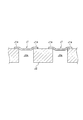
この場合、基板上に有機EL素子を形成する素子形成工程は、多数のパネル分の成膜工程を同時に行うことができるので、製造時間の短縮化が可能になる。この際、各有機EL素子部の封止は、図1に示すように、ロボットアームを利用して各有機EL素子部の数(数10個~数100個)の封止缶J1を搬送トレイ(搬送手段)J2に整列させる。そして、UV硬化接着剤を封止缶J1のフランジ部分J1aに塗布し、真空室内を通過させ脱泡・ガス出しの自動化工程を経て封止チャンバに送り込み、多数の封止缶J1を搬送トレイJ2ごと大判基板に押し当てて一括同時にUV接着を行う。
このように、大判基板上に形成された各有機EL素子部上に位置精度良く封止缶を貼り付けるには、ロボットアーム等の位置決め精度が高く、振動が少ない搬送手段が必要になる。図1に示したような搬送トレイJ2は、封止缶J1の位置決めをするために非常に高い精度が要求され、更には封止缶J1の一個一個を搬送トレイJ2の対応した位置に速く正確に並べるには前述したロボットアーム等の高価な搬送装置が必要になるので、設備費が高額化する問題がある。また、搬送トレイJ2への配列数が増加すると、それに応じて配列のための作業時間に長時間を要することになり、高い生産性が得られなくなる問題もある。
また、図1に示したような搬送トレイJ2には、封止缶J1が嵌合する部分に位置決め穴J2aが形成されており、その位置決め穴J2aの周囲に封止缶J1のフランジ部分J1aが保持されている。このような搬送トレイJ2を用いて、封止缶J1を密に配列しようとしたとき、封止缶J1間の保持部分が細くなり搬送トレイJ2の精度が低下してしまうし、フランジ部分J1aを短くして位置決め穴J2a間を狭くすると、僅かな振動で封止缶J1がずれたり、必要な封止性能が得られないので、一定以上に密には配列できない問題がある。したがって、このような搬送トレイJ2を使用する方式では、大判基板上に集約できる有機ELパネルの形成密度に限界があり、これが生産性向上の妨げになると共に、有機EL素子部以外のパネル面積が大きくなって、有機ELパネル設置時のスペース効率が悪くなる問題がある。
これに対して、特許文献3及び特許文献4のように、大判の金属板に複数の封止凹部をプレス成形やエッチングで形成し、大判の金属板を大判基板に貼り付けることも考えられるが、これによると、貼り付け後の金属板の分断が困難になる。また、封止部材を連結した状態で作成する等の製造工程が複雑になる問題がある。
また、有機ELパネルを各種機器に実装するに際して、特許文献5に記載されるようにパネルとフレームとを一体成形した場合、フレームの厚さ分だけ実装スペースを余分に取ることになるので機器内でのスペース効率が悪くなる問題がある。また、樹脂材料による型枠成型を行った場合には、有機EL素子を封止後に高温に曝すことになるので、高温による発光特性の劣化を生じさせない工夫が必要になる。
本発明は、このような問題に対処することを課題の一例とするものである。すなわち、有機ELパネルの生産性及び品質を向上させること、有機ELパネルの生産数量を拡大して生産コストの削減を図ること、有機ELパネルの実装スペース効率を向上させること、等が本発明の目的である。
このような目的を達成するために、本発明による有機ELパネルの製造方法及び有機ELパネルは、以下の各独立請求項に係る構成を少なくとも具備するものである。
[請求項1]個別の有機ELパネルの基板になる個別領域を複数含む透明な1枚の被分割基板上に、前記個別領域毎に単数又は複数の有機EL素子からなる素子部を形成する素子部形成工程と、1枚の封止シートに、前記被分割基板上の各素子部を封止する複数の封止部と該封止部を分断可能に当該封止シートに連結する連結部を画定する封止部画定工程と、前記被分割基板上又は前記封止シート上に、前記封止部の内側で前記素子部を囲むように前記個別領域毎に接着剤層を形成し、前記被分割基板と前記封止シートとを前記接着剤層を介して貼り合わせる貼合工程と、前記封止シートから各封止部を分断すると共に、前記被分割基板を前記個別領域毎に分割して、前記基板に前記封止部を貼り合わせた個別の有機ELパネルを得る分断・分割工程とを有し、前記封止部画定工程は、前記封止シートの一面側を部分的にエッチングして、前記封止部の外縁に沿った第1の溝部を形成する第1のエッチング工程と、前記封止シートの他面側を部分的にエッチングして、前記封止部の外縁に沿った前記第1の溝部を貫通させる第2の溝部を形成する第2のエッチング工程を有し、前記連結部とパネル装着時の係止部になるパターンを前記封止部の外縁に対して形成し、前記分断・分割工程後に前記パターンを有機ELパネルの表示部と反対側に突出するように折り曲げ加工して前記係止部を形成することを特徴とする有機ELパネルの製造方法。
[請求項1]個別の有機ELパネルの基板になる個別領域を複数含む透明な1枚の被分割基板上に、前記個別領域毎に単数又は複数の有機EL素子からなる素子部を形成する素子部形成工程と、1枚の封止シートに、前記被分割基板上の各素子部を封止する複数の封止部と該封止部を分断可能に当該封止シートに連結する連結部を画定する封止部画定工程と、前記被分割基板上又は前記封止シート上に、前記封止部の内側で前記素子部を囲むように前記個別領域毎に接着剤層を形成し、前記被分割基板と前記封止シートとを前記接着剤層を介して貼り合わせる貼合工程と、前記封止シートから各封止部を分断すると共に、前記被分割基板を前記個別領域毎に分割して、前記基板に前記封止部を貼り合わせた個別の有機ELパネルを得る分断・分割工程とを有し、前記封止部画定工程は、前記封止シートの一面側を部分的にエッチングして、前記封止部の外縁に沿った第1の溝部を形成する第1のエッチング工程と、前記封止シートの他面側を部分的にエッチングして、前記封止部の外縁に沿った前記第1の溝部を貫通させる第2の溝部を形成する第2のエッチング工程を有し、前記連結部とパネル装着時の係止部になるパターンを前記封止部の外縁に対して形成し、前記分断・分割工程後に前記パターンを有機ELパネルの表示部と反対側に突出するように折り曲げ加工して前記係止部を形成することを特徴とする有機ELパネルの製造方法。
[請求項7]有機EL素子を有する素子部が形成された基板と、前記素子部を封止するように前記基板に貼り合わせられた封止部とを備え、前記封止部は、封止シートから分断された連結部を外縁の一部に備え、その外縁が前記封止シートの一面側からエッチングされた第1のテーパ付きエッチング処理面と前記封止シートの他面側からエッチングされた第2のテーパ付きエッチング処理面によって形成され、前記連結部を有機ELパネルの表示部と反対側に突出するように折り曲げ加工したパネル装着時の係止部を有することを特徴とする有機ELパネル。
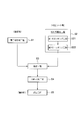
以下、本発明の実施形態を図面を参照して説明する。図2は本発明の一実施形態に係る有機ELパネルの製造方法の概略を示す説明図である。この製造方法は、基板側の工程として、基板(被分割基板)上に有機EL素子からなる素子部を形成する素子部形成工程S1と、封止シート側の工程として、第1のエッチング工程S21と第2のエッチング工程S22からなり、封止シートに複数の封止部と該封止部を分断可能に当該封止シートに連結する連結部を画定する封止部画定工程S2と、前述の被分割基板と封止シートとを接着剤層を介して貼り合わせる貼合工程S3と、封止シートから各封止部を分断すると共に、被分割基板を個別領域毎に分割して、基板に封止部を貼り合わせた個別の有機ELパネルを得る分断・分割工程S4と、有機ELパネルを装着する表示機器の筐体側の工程として、筐体に有機ELパネルを装着する組立工程S5を有する。
本発明の実施形態に係る有機ELパネルの製造方法によると、複数の封止部をシート状に連結した封止シートを形成し、この封止シートと有機EL素子からなる素子部が形成された基板とを貼り合わせて、各素子部を各封止部で封止し、その後、基板に貼り付けられた封止部を除いた封止シートを一度にシート状に引き剥がすことで、各封止部を簡易に分断可能にしたものであり、分断される封止部と封止シートとの連結部を利用してパネルを表示機器に装着する際の係止部を形成したものである。以下に、前述した各工程を具体的に説明する。
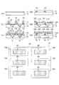
図3は、前述した素子部形成工程を説明する説明図である((a1)~(c1)及び(a2)~(c2)が各工程を説明する断面説明図、(d)が平面説明図)。素子部形成工程S1は、個別の有機ELパネルの基板になる個別領域10Aを複数含む透明な1枚の被分割基板10上に、個別領域10A毎に単数又は複数の有機EL素子pからなる素子部20を形成する。
同図(a1)~(c1)は、パッシブ駆動方式の有機EL素子pを形成する工程の一例を示している。先ず、同図(a1)に示すように、被分割基板10上に第1電極11をストライプ状にパターニングして形成する。被分割基板1は、ガラスや石英,樹脂等の透明ないし半透明の材料からなるものから形成される。第1電極11から延長される引き出し配線或いは後述する第2電極に接続される引き出し配線を同時に形成することができる。
次に、同図(b1)に示すように、第1電極11及び被分割基板10上に画素領域gを開けて絶縁膜12を成膜及びパターニングすると共に、第1電極11と交差するように絶縁膜12上にストライプ状の隔壁13を形成する。
次に、同図(c1)に示すように、画素領域gを覆って、第1電極11上に発光層を含む有機層14を成膜し、有機層14の上に、隔壁13によって第1電極11と交差するように絶縁区画されるストライプ状に第2電極15を成膜する。
同図(a2)~(c2)は、アクディブ駆動方式の有機EL素子pを形成する工程の一例を示している。同図(a2)に示すように、駆動素子16を備えた被分割基板10上に平坦化膜17を形成する。そして、同図(b2)で示すように、その平坦化膜17上に駆動素子16に接続された第1電極(画素電極)11Aをドットマトリクス状に形成し、第1電極11A上の画素領域gを開けて第1電極11Aを絶縁膜12Aで区画する。その後、同図(c2)に示すように、画素領域gを覆うように、第1電極11A上に発光層を含む有機層14Aを成膜し、その上に、各有機層14Aに共通する第2電極15Aを成膜する。
被分割基板10上に形成される有機EL素子pからなる複数個の素子部20の各形成工程は同時工程で行われる。したがって、個々に基板上に素子部20を形成する場合と比較して形成時間を個数分の1以下に削減できる。
第1電極11を陽極として、第2電極15を陰極とした場合の有機層14の形成例(パッシブ駆動方式の例)を以下に示す。
第1電極11上に銅フタロシアニン(CuPc)等の正孔注入層を形成し、その上に、例えば、NPB(N,N-di(naphtalence)-N,N-dipheneyl-benzidene)を正孔輸送層として成膜する。この正孔輸送層は、第1電極11から注入される正孔を発光層に輸送する機能を有する。この正孔輸送層は、1層だけ積層したものでも2層以上積層したものであってもよい。また正孔輸送層は、単一の材料による成膜ではなく、複数の材料により一つの層を形成しても良く、電荷輸送能力の高いホスト材料に電荷供与(受容)性の高いゲスト材料をドーピングしてもよい。
次に、正孔輸送層の上に発光層を成膜する。一例としては、抵抗加熱蒸着法により、赤(R)、緑(G)、青(B)の発光層を、塗分け用マスクを利用してそれぞれの成膜領域に成膜する。赤(R)としてDCM1(4-(ジシアノメチレン)-2-メチル-6-(4’-ジメチルアミノスチリル)-4H-ピラン)等のスチリル色素等の赤色を発光する有機材料を用いる。緑(G)としてアルミキノリノール錯体(Alq3) 等の緑色を発光する有機材料を用いる。青(B)としてジスチリル誘導体、トリアゾール誘導体等の青色を発光する有機材料を用いる。勿論、他の材料でも、ホスト-ゲスト系の層構成でも良く、発光形態も蛍光発光材料を用いてもりん光発光材料を用いたものであってもよい。
発光層の上に成膜される電子輸送層は、抵抗加熱蒸着法等の各種成膜方法により、例えばアルミキノリノール錯体(Alq3 )等の各種材料を用いて成膜する。電子輸送層は、第2電極15から注入される電子を発光層に輸送する機能を有する。この電子輸送層は、1層だけ積層したものでも2層以上積層した多層構造を有してもよい。また、電子輸送層は、単一の材料による成膜ではなく、複数の材料により一つの層を形成しても良く、電荷輸送能力の高いホスト材料に電荷供与(受容)性の高いゲスト材料をドーピングして形成してもよい。
第2電極15は、例えば、第1電極11のパターンと直交する方向に沿ってストライプ状にパターニングされる。この際、絶縁膜12上に隔壁13を形成する場合には、この隔壁13をマスクパターンとして利用して、第2電極15のパターン形成を行うことができる。絶縁膜12や隔壁13はポリイミドやレジスト材料から構成される。第2電極15は、陰極として機能する場合には、電子注入機能を有するように、陽極より仕事関数の低い材料を用いる。例えば、陽極としてITOを用いた場合には、アルミニウム(Al)やマグネシウム合金(Mg-Ag)を利用するのが好ましい。但し、Alは電子注入能力が低いためにAlと電子輸送層との間にLiFのような電子注入層を設けることが好ましい。
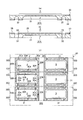
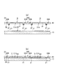
図4は、前述した封止部画定工程を示す説明図である。同図(a)が第1のエッチング工程、同図(b)が第2のエッチング工程を示しており、同図(c)が画定された封止部及び連結部の平面図を示している。封止シート30は、経時的変化が少なく接着剤の乖離や基板のそりを防止するため熱膨張係数が基板に近い材料を用いることが好ましく、ステンレスやアルミニウムなどの金属材,合金等を利用することができる。後の係止部の形成のためには簡易に折り曲げ加工が可能な材料が好ましい。
前述した封止部画定工程S2は、1枚の封止シート30に、被分割基板10上の各素子部20(図2参照)を封止する複数の封止部3と封止部3を分断可能に封止シート30に連結する連結部30Aを画定する工程である。また、封止部画定工程S2は、封止シート30の一面側を部分的にエッチングして、各素子部20に対応する封止空間31Aを形成する凹部31と封止部3の外縁に沿った第1の溝部32を形成する第1のエッチング工程S21(同図(b))と、封止シート30の他面側を部分的にエッチングして、封止部3の外縁に沿って第1の溝部32を貫通させる第2の溝部33を形成する第2のエッチング工程S22(同図(b))を有する。ここで、凹部31は、封止部3をスペーサ又は所定厚さの接着層を介して被分割基板10に貼り付ける場合には省略することができる。
前述した第1のエッチング工程S21は、同図(a)に示すように、第1のエッチングマスク34を介した封止シート30の一方の面に対するエッチング処理によって、凹部31と第1の溝部32を形成する。凹部31は、前述した素子部20を囲む封止空間31Aを形成するものであり、被分割基板10上の各素子部20の形成位置に対応して、封止シート30に形成される。第1の溝部32は、分断可能な連結部30Aを除いた各封止部3の外縁を囲って環状に形成される。凹部31と第1の溝部32は、エッチングマスク34のパターンとして同時に形成され、その深さは、最大深さが封止シート30の厚さの約半分程度になるように形成されるのが望ましいが、深さは半分程度に限定されない。封止空間31Aは内部に設置した乾燥剤と有機EL素子との接触を防ぐために深くする場合もあり、封止シート30の強度を保つために封止空間31Aを浅くする場合もある。
前述した第2のエッチング工程S22は、同図(b)に示すように、第2のエッチングマスク35を介した封止シート30の他方の面に対するエッチング処理によって、第2の溝部33を形成する。第2のエッチングマスク35は、同図(c)に示した貫通部30B(斜線で示す)を除く全ての部分を覆うように形成される。したがって、第2の溝部33は、連結部30Aを除いた第1の溝部32に沿って形成されることになり、連結部30Aを除いた第1の溝部32に沿って、貫通部30Bが形成されることになる。また、第1のエッチング工程S21もしくは第2のエッチング工程S22において、第1の溝部32又は第2の溝部33を封止部3の全周にわたって環状に形成した場合には、連結部30Aは、封止シート30の厚さの半分程度になって、分断しやすい状態になる。また、平面視した連結部30Aの端部をくびれた状態にすることで、さらに分断しやすくすることができる。
第2の溝部33は、貫通部30Bにおいて封止シート30が完全に貫通する深さに形成される。また、第2の溝部33の外側に不要部30Cが形成されることになる。第1の溝部32を環状に形成して、第2の溝部33が連結部30Aを除く部分に形成してもよいし、それとは逆に、第2の溝部33を環状に形成し、第1の溝部32が連結部30Aを除く部分に形成されるようにしてもよい。
封止部画定工程S2において、最終的に封止部3を分断可能に画定した封止シート30は、同図(c)に示すような形態を有し、平面的には、封止部3,連結部30A,貫通部30B,不要部30Cに区画されることになる。また、封止部を分断する際の作業を容易にするために、不要部30Cにミシン目のような切れ目30Dを形成しておくこともできる。この切れ目30Dは、貫通部30Bの両端に沿って平行に形成される。切れ目30Dは、これに限らず、不要部30Cに、一列に並んだ封止部3の中心に沿って一直線上に形成してもよい。また、切れ目30Dを第1のエッチング工程S21もしくは第2のエッチング工程S22と同時に形成することにより封止部を分断する作業を容易にすることができる。
図5~図8は、前述した封止部画定工程S2によって形成される封止部の形態例を具体的に示した平面図である。図5は、同図(a)が平面図、同図(b)がA部拡大図、同図(c)がB部拡大図を示している。この実施形態では、連結部30Aが封止部3と反対側の端部30AS1で幅狭状(幅S1)にパターン形成されており、封止部3側の端部30AS2でもやや幅狭状(幅S2>S1)にパターン形成されている。これによると分断時により幅が狭くパターニングされた端部30AS1で分断がなされるので、連結部30Aを所定の長さに保った状態で封止部3側に残すことができる。これによって、表示機器筐体側へ有機ELパネルを係止するのに十分な長さを有する係止部を連結部30Aによって形成することができる。また、封止部3側の端部30AS2をやや幅狭状にすることで、連結部30Aを端部30AS2から簡易に折り曲げ加工することができる。この端部30AS2はその厚さを薄厚状にすることで、より折り曲げ加工がし易くなり、連結部30Aをその基部から略直角に折り曲げることも可能になる。
図6は、同図(a)が平面図、同図(b)がA-A断面図を示している。この実施形態では、連結部30Aが封止部3と反対側の端部30AS3で薄厚状にパターン形成されており、封止部3側の端部30AS4でも薄厚状にパターン形成されている。これによると分断時に端部30AS3で分断して、連結部30Aを所定の長さに保った状態で封止部3側に残すことができる。また、封止部3側の端部30AS4を薄厚状にすることで、連結部30Aを端部30AS4から簡易に折り曲げ加工して係止部を形成することができる。図5に示した幅狭状のパターンと図6に示した薄厚状のパターンは、それぞれ単独で形成しても良いし、それらを組み合わせて、幅狭状且つ薄厚状のパターンに形成しても良い。
図5及び図6に示した実施形態では、連結部30Aの長さをある程度長く設定すると、封止シート30内に配列される封止部3間の間隔が大きくなって、封止シート30内に高密度に封止部3を画定することができない。これを解消するための実施形態が図7に示した例である。同図(a)に示した例では、封止部3の側辺に沿って連結部30Aを所定の長さで形成し、その連結部30Aの一端を封止部3側に連結し、他端を不要部30C側に連結している。不要部30C側の端部を分断することで、封止部3側に所定長さの連結部30Aを残すことができる。連結部30Aを折り曲げ加工して係止部を形成する際には、図示のa点を捩るようにして連結部30Aをパネルの表示部と反対側に立ち上げるか、或いはb線に沿って折り曲げて連結部30Aをパネルの表示部と反対側に立ち上げる。
同図(b)に示した例では、隣り合う封止部3における連結部30Aの位置をずらして、連結部30Aの長さが互いに重なるようにパターン形成している。これによっても、連結部30Aの長さを十分に確保しながら、隣接する封止部3の間隔を狭くすることが可能になる。
図5~図7では、連結部30Aを形成するパターンを折り曲げ加工することによって係止部を形成する例を説明した。本発明の実施形態では、これに限らず、連結部30Aとは別のパターンによって係止部を形成することもできる。図8はこの例を示した平面図である。この例では、連結部30Aとは別に、一端側が封止部3側に一体になっており、他端側が不要部30Cとは離れた係止部パターン30Dが形成されている。この係止部パターン30Dは封止部3側から片持ち状態で突出して形成されており、これがパネルの表示部とは逆方向に折り曲げられて係止部になる。
図9は、前述した貼合工程を説明する説明図(説明断面図)である。同図(a)が貼り合わせ前の状態、同図(b)が貼り合わせ後の状態を示している。前述した貼合工程S3は、被分割基板10上又は封止シート30上に、封止部3の内側で素子部20を囲むように個別領域毎に接着剤層21を形成し、被分割基板10と封止シート20とを接着剤層21を介して貼り合わせる工程である。
封止シート30において、凹部31の外側と貫通部30Bの内側の平面的なスペースが被分割基板10と封止シート30の接着領域となり、そのスペースに沿って接着剤が塗布されて、接着剤層21が形成される。すなわち、連続した環状に形成された第1の溝部32の内側に沿って接着剤層21が形成されることになる。
接着剤層21は、同図(a)に示すように、封止シート30側と被分割基板10の一方又は両方に形成され、何れの場合にも、素子部20を完全に囲むように環状に形成される。接着剤としては、紫外線硬化型又は熱硬化型樹脂を用いることができる。封止シート30の凹部31内には必要に応じて乾燥剤が配備される。
被分割基板10と封止シート30と貼り合わせは、窒素ガス雰囲気中等の封止室内で行われ、被分割基板10と封止シート30とを位置合わせした後、同図(b)に示すように貼り合わせ、加圧した状態で接着剤の硬化処理を行う。図示の例のように、連結部30Aを第2の溝部33のパターンによって形成した場合には、接着剤層21の外側には全周に第2の溝部32が形成されることになるので、この場合には、貼り合わせ時に接着剤層21が連結部30Aを通して外に広がることを第2の溝部32によって防止することができる。
貼合工程S3の後に行われる分断・分割工程S4は、前述した封止シート30から個別の封止部3を分断し、被分割基板10から個別の基板を分割して、個別の有機ELパネルを得る工程である。
図10は、封止シート30から封止部3を分断する工程を示した説明図である。前述した封止シート30における連結部30Aは、第1の溝部32又は第2の溝部33によって薄厚化されている部分であるから、弱い剪断力であっても容易に切断可能な部分になっている。この連結部30Aに適度の剪断力を加えることによってこれを切断し、接着されている封止部3を被分割基板10上に残して、不要部30Cを封止部3から分断して被分割基板10からシート状に引き剥がす。不要部30Cには位置決め孔30Pが必要に応じて形成されている。
この分断時には、封止シート30の不要部30Cは、封止部3が抜けた状態の繋がったシートとして一括して剥がすことができる。したがって、一連の工程で封止シート30における不要部30Cをシート状に引き剥がすことができ、簡易且つ効率的に被分割基板30上に接着された封止部3のみを残すことができる。
連結部30Aの強度が強い場合、不要部30Cの引き剥がしに伴い封止部3も剥離する虞がある。これを防止するためには、直線上の押さえ治具51で封止部3を押さえながら不要部30Cを引き剥がす。これにより、封止部3を剥離させることなく、封止部3と不要部30Cを分断することができる。この時、封止シート30の不要部30Cに、一列に並んだ封止部3の両側に沿って平行に切れ目30Dを形成することが必要になる。基板1を吸着などで固定し、一列に並んだ封止部3を押さえる直線状の押さえ治具等で封止部3を押さえた状態で、連結部30A及び切れ目30Dを破って押さえ部材を交わしながら、封止部3から不要部30Cを分断する。
押さえ治具51が一本である場合は、不要部30Cの引き剥がし動作に伴い隣接する封止部と、その連結部30Aにも力が働き、封止部3が剥離する虞がある。図11は、押さえ治具を用いた分断工程の一例を示した説明図である。同図(a)が平面図、同図(b)が側面図を示している。これによると、平坦な支持面を有する支持台50上に貼り合わせられた封止シート30と被分割基板10を設置し、その上に押さえ治具51を載せて、クランプ52で左右端をそれぞれ押圧固定する。押さえ治具51は、封止シート30における封止部3の一列ごとに一本が対応するように配置され、複数列に配列された封止部3を複数本の押さえ治具51を用いて押さえている。
この状態で、封止シート30の一端側から被分割基板10に接着されていない不要部30Cのみを矢印のように引き上げ、連結部30Aを切断して、封止部3と不要部30Cとを分断する。この際、前述した切れ目30Dを設けておくことで、押さえ治具51を交わして不要部30Cのみを引き上げることができる。この引き上げ時に、引き上げられる直前の位置で押さえ治具51を押圧する押さえローラ53を用いることで、封止部3を被分割基板10から剥離させることなくより確実に封止部3から不要部30Cを分断させることができる。
図12は、被分割基板10を分割する工程を示した説明図(説明断面図)である(前述の説明と共通箇所は同一符号を付して重複説明を省略する)。封止部3が接着された被分割基板10を個別領域10A毎に分割する。分割に際しては、カットラインLに沿って分割工具(例えば、ダイヤモンドカッター)60の刃を押し当てる。これによって、被分割基板10が個別領域10A毎に分割して、個別の有機ELパネルを得ることができる。
図13は、前述した封止シート30の分断工程に先だって、被分割基板10を分割する例を示している。この場合には、被分割基板10を個別領域10A毎に分割した後に、封止シート30から各封止部3を分断する。ここでは、封止シート30が支持面を形成するので、被分割基板10の裏面(素子部20を形成していない面)側から分断工具60の刃を当てて、封止部3の外縁に沿って分断することができる。これによると、刃の厚みを考慮しないで封止部3の外縁に沿ってカットラインLを設定することができるので、被分割基板10の個別領域10Aを必要最小にすることができ、有機ELパネルのスペース効率を向上させることができる。これによると、有機ELパネルの配列数を増加することができ、大判1枚当たりの有機ELパネルの取り数を多くすることができる。
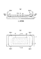
図14は、前述した製造方法で形成された有機ELパネルを示す説明図である。同図(a)が断面図(X-X断面図)、同図(b)が平面図を示している。有機ELパネルは、前述した被分割基板10から分割された基板1上に素子部20が形成されており、素子部20を覆う封止空間31Aを有する前述した封止シート30から分断された封止部3が、基板1上に接着剤層21を介して接着されている。
ここで、前述した製造方法で形成された有機ELパネルは、封止部3の外縁に、一面側からの前述の第1のエッチング工程S21によって形成された第1のテーパ付きエッチング処理面3S1と、他面からの前述の第2のエッチング工程S22によって形成された第2のテーパ付きエッチング処理面3S2が形成されている。また、前述した製造方法で形成された有機ELパネルは、封止部3の外縁に、係止部30A1が数カ所に形成されている。この係止部30A1は、封止部3側に残った連結部30Aを有機ELパネルの表示部と反対側に突出するように折り曲げ加工したものである。連結部30Aの折り曲げは、不要部30Cの引き剥がしに伴って行うことができるが、それとは別に成形機等で必要な形状に折り曲げ加工しても良い。
このような本発明の実施形態に係る有機ELパネルの製造方法によると、先ず、1枚の封止シート30に複数の封止部3を画定し、複数の素子部20が形成された被分割基板10と封止シート30とを貼り合わせて、被分割基板10上の複数の素子部20を一度に複数の封止部3で覆うようにしたので、被分割基板10上の複数の素子部20に個々の封止部を被せる場合と比較して、貼合工程S3の処理時間を大幅に短縮することができる。
また、封止部3は、封止シート30内の正確な位置でそれぞれ画定されているので、封止シート30と被分割基板10を位置決めすれば、被分割基板10上の全ての素子部20と封止シート30内の全ての封止部3が位置決めされることになり、貼り合わせ前の位置決めを簡易且つ短時間で行うことができる。
また、被分割基板10上の複数の素子部20を同時に封止することができるので、一枚の被分割基板10から形成される有機ELパネルの品質を均一化することができる。
封止部画定工程S2では、第1のエッチング工程S21と第2のエッチング工程S22のみで、封止空間31Aを形成する凹部31、封止部3と不要部30Cとを区分けする貫通部30B、分断し易いように厚さが薄く形成された連結部30Aをそれぞれ形成することができる。特に、凹部31の溝深さと連結部30Aの溝深さを一致させることで、第1のエッチング工程S21の一回の処理で、凹部31を形成するための溝と連結部30Aを形成するための溝を同時に形成することができる。よって、エッチング処理に要する時間を効率化することができる。また、第1のエッチング工程S21と第2のエッチング工程S22を同時に処理することによりエッチングに要する時間を効率化できる。
また、封止部画定工程S2は、エッチング処理のみで行われ、プレス加工や打ち抜き加工を施さないので、封止シート30に加工歪みが生じることが無く、加工面の後処理(バリ除去)等が不要になると共に、画定位置の寸法精度を向上させることができる。
分断・分割工程S4では、連結部30Aを切断することで、第2の溝部の外側に形成される封止シート30の不要部30Cが繋がった状態で、被分割基板10に接着された封止部3から不要部30Cを分断する。これによると、シート状に引き剥がす要領で、簡易に、被分割基板10に接着された封止部3と不要部30Cとを分断することができる。また、不要部30Cが繋がった状態で分断されるので、引き剥がされた不要部30Cの回収が容易である。
また、封止部画定工程S2で、封止シート30の不要部30Cに、一列に並んだ封止部3に沿った一直線上の切れ目30Dを形成し、分断・分割工程S4では、一列に並んだ封止部3を押さえる直線状の押さえ治具51で封止部3を押さえた状態で、連結部30A及び切れ目30Dを破って押さえ治具51を交わしながら、封止部3から不要部30Cを引き剥がすことができるので、不要部30Cを引き剥がす際に、接着された封止部3が被分割基板10から剥がれるのを防止することができる。また、押さえ治具51のエッジ部を連結部30Aに当てて不要部30Cを引き剥がすことにより、連結部30Aに効果的な剪断力を加えることができ、容易に連結部30Aを切断して、被分割基板10から不要部30Cを引き剥がすことができる。
分断・分割工程S4は、前述したように、封止シート30において封止部3と不要部30Cとを分断する工程と、被分割基板10を個別領域10A毎に分割する工程の何れを先に行っても良い。先に、被分割基板10を個別領域10A毎に分割した場合でも封止シート30が一連に繋がっているために封止部3と不要部30Cを分断できる。被分割基板10の個別領域10Aを必要最小に小型化し、有機ELパネルのスペース効率を向上させることができる。
被分割基板10を分割した後に、封止シート30の分断を行う場合には、例えば、図11に示すような設備を用い、支持台50上に封止シート30とこれに接着された基板1を設置し、全ての基板1上に押さえ治具51が載せられるようにして押圧固定する。この状態で、封止シート30の不要部30Cをシート状に引き剥がす。
前述した貼合工程S3では、封止部3の外縁の全周に沿って形成される第1の溝部32の内側に接着剤層21が形成されることになる。これによると、被分割基板10と封止シート30との貼り合わせ時に接着剤層21が押圧されて広がったとしても、この広がりを第1の溝部32が遮って不要部30Cと被分割基板10とが接着されることを防いでいる。これによって、分断・分割工程S4での封止シート30の引き剥がしを円滑に行うことができる。
このような本発明の実施形態に係る製造方法によって得られた有機ELパネルは、図14に示すように、封止部3の外縁には、一面側からの第1のエッチング工程S21によって形成された第1のテーパ付きエッチング処理面3S1と、他面からの第2のエッチング工程S22によって形成された第2のテーパ付きエッチング処理面3S2が形成されると共に、封止部3側に残った連結部30Aを表示部と反対側に突出するように折り曲げ加工することによって係止部30A1が数カ所に形成されることになる。これによると、封止部3の外縁がエッチング処理によって形成されることで外周のエッジ部に対してバリ除去等の後処理を施す必要がない。また、係止部30A1は、有機ELパネルを携帯電話やカーステレオなどの各種表示機器に装着する際の係止突起として活用し、組立工程を迅速化することができる。
図15は、本発明の実施形態における組立工程を説明するための説明図である。同図(a)は、本発明の実施形態に係る有機ELパネルが装着される表示機器の一例を示すもので、ここでは表示部101を有する携帯電話100を例示している。携帯電話100は一般に表示部101の他にスピーカ102,操作部103,マイク104等を備えている。
同図(b)は、前述した携帯電話100に対して有機ELパネルを装着する組立工程を示した説明図である。携帯電話100の筐体100Aには係止孔(被係止部)100A1が備えられており、その係止孔に対して有機ELパネルPの係止部30A1が係止される。係止部30A1は前述したようにパネルの表示面P1とは反対側に表示面P1に対して垂直に突出するように形成されている。この係止部30A1を係止孔100A1に係止して、その後に有機ELパネルPの表示面P1に開口110Aが合致するように上面部材110を装着する。
同図(c)は、筐体100Aに本発明の実施形態に係る有機ELパネルPを装着した状態を示した説明図である。封止部3の表面を筐体100Aの取付面に当接させ、係止孔100A1に係止部30A1を挿入している。挿入後に係止部30A1の先端を折り曲げて筐体100Aに対して有機ELパネルPを抜け止め状態に固定することもできる。この際、係止部30A1は封止部3と一体に形成されているので、取り付けフレームなどを別途有機ELパネルPに一体化させる手間が省けると共に、取り付けのために要するスペースを最小限に抑えることができる。これによって、小型の表示機器にスペース効率よく有機ELパネルPを装着することができる。
また、本発明の実施形態に係る有機ELパネルでは、係止部30A1は封止シート30から封止部3を分断することで形成されるので、簡単な折り曲げ加工を施すだけで簡易に係止部30A1を追加することができる。係止部30A1の位置は封止部画定工程S2のエッチング工程で位置決めされるので、封止部3における所望の位置に正確に形成することができる。これによって、組立工程S5においても筐体に精度良く有機ELパネルを位置決めすることができる。
Claims (10)
- 個別の有機ELパネルの基板になる個別領域を複数含む透明な1枚の被分割基板上に、前記個別領域毎に単数又は複数の有機EL素子からなる素子部を形成する素子部形成工程と、
1枚の封止シートに、前記被分割基板上の各素子部を封止する複数の封止部と該封止部を分断可能に当該封止シートに連結する連結部を画定する封止部画定工程と、
前記被分割基板上又は前記封止シート上に、前記封止部の内側で前記素子部を囲むように前記個別領域毎に接着剤層を形成し、前記被分割基板と前記封止シートとを前記接着剤層を介して貼り合わせる貼合工程と、
前記封止シートから各封止部を分断すると共に、前記被分割基板を前記個別領域毎に分割して、前記基板に前記封止部を貼り合わせた個別の有機ELパネルを得る分断・分割工程とを有し、
前記封止部画定工程は、
前記封止シートの一面側を部分的にエッチングして、前記封止部の外縁に沿った第1の溝部を形成する第1のエッチング工程と、前記封止シートの他面側を部分的にエッチングして、前記封止部の外縁に沿った前記第1の溝部を貫通させる第2の溝部を形成する第2のエッチング工程を有し、前記連結部とパネル装着時の係止部になるパターンを前記封止部の外縁に対して形成し、
前記分断・分割工程後に前記パターンを有機ELパネルの表示部と反対側に突出するように折り曲げ加工して前記係止部を形成することを特徴とする有機ELパネルの製造方法。 - 前記連結部を形成するパターンによって前記係止部が形成されることを特徴とする請求項1に記載された有機ELパネルの製造方法。
- 前記連結部とは別のパターンによって前記係止部が形成されることを特徴とする請求項1に記載された有機ELパネルの製造方法。
- 前記連結部を形成するパターンは、前記封止部と反対側の端部が薄厚状又は幅狭状にパターン形成されていることを特徴とする請求項2に記載の有機ELパネルの製造方法。
- 前記係止部を形成するパターンは、前記封止部側の端部が薄厚状又は幅狭状にパターン形成されていることを特徴とする請求項1又は2に記載の有機ELパネルの製造方法。
- 前記分断・分割工程では、
前記連結部を切断することで、前記第2の溝部の外側に形成される前記封止シートの不要部が繋がった状態で、前記被分割基板に接着された前記封止部から前記不要部を分断することを特徴とする請求項1~5のいずれかに記載の有機ELパネルの製造方法。 - 有機EL素子を有する素子部が形成された基板と、
前記素子部を封止するように前記基板に貼り合わせられた封止部とを備え、
前記封止部は、封止シートから分断された連結部を外縁の一部に備え、その外縁が前記封止シートの一面側からエッチングされた第1のテーパ付きエッチング処理面と前記封止シートの他面側からエッチングされた第2のテーパ付きエッチング処理面によって形成され、
前記連結部を有機ELパネルの表示部と反対側に突出するように折り曲げ加工したパネル装着時の係止部を有することを特徴とする有機ELパネル。 - 前記連結部は前記封止部と反対側の端部が幅狭状又は薄厚状にパターン形成されていることを特徴とする請求項7に記載の有機ELパネル。
- 前記連結部は前記封止部側の端部が幅狭状又は薄厚状にパターン形成されていることを特徴とする請求項7又は8に記載の有機ELパネル。
- 請求項7~9のいずれかに記載された有機ELパネルを表示部とする表示機器であって、
前記係止部が係止される被係止部を有する筐体を備えていることを特徴とする表示機器。
Priority Applications (1)
| Application Number | Priority Date | Filing Date | Title |
|---|---|---|---|
| PCT/JP2008/062948 WO2010007682A1 (ja) | 2008-07-17 | 2008-07-17 | 有機elパネルの製造方法及び有機elパネル、表示機器 |
Applications Claiming Priority (1)
| Application Number | Priority Date | Filing Date | Title |
|---|---|---|---|
| PCT/JP2008/062948 WO2010007682A1 (ja) | 2008-07-17 | 2008-07-17 | 有機elパネルの製造方法及び有機elパネル、表示機器 |
Publications (1)
| Publication Number | Publication Date |
|---|---|
| WO2010007682A1 true WO2010007682A1 (ja) | 2010-01-21 |
Family
ID=41550100
Family Applications (1)
| Application Number | Title | Priority Date | Filing Date |
|---|---|---|---|
| PCT/JP2008/062948 Ceased WO2010007682A1 (ja) | 2008-07-17 | 2008-07-17 | 有機elパネルの製造方法及び有機elパネル、表示機器 |
Country Status (1)
| Country | Link |
|---|---|
| WO (1) | WO2010007682A1 (ja) |
Citations (4)
| Publication number | Priority date | Publication date | Assignee | Title |
|---|---|---|---|---|
| JP2004079467A (ja) * | 2002-08-22 | 2004-03-11 | Nippon Sheet Glass Co Ltd | El素子用封止板、及び該封止板多面取り用マザーガラス基板 |
| JP2007234331A (ja) * | 2006-02-28 | 2007-09-13 | Tohoku Pioneer Corp | 自発光パネルの封止用部材、自発光パネルの製造方法、および自発光パネル |
| JP2007234332A (ja) * | 2006-02-28 | 2007-09-13 | Tohoku Pioneer Corp | 自発光パネルの製造方法、および自発光パネル |
| JP2007273400A (ja) * | 2006-03-31 | 2007-10-18 | Tohoku Pioneer Corp | 光デバイスの製造方法、および光デバイス |
-
2008
- 2008-07-17 WO PCT/JP2008/062948 patent/WO2010007682A1/ja not_active Ceased
Patent Citations (4)
| Publication number | Priority date | Publication date | Assignee | Title |
|---|---|---|---|---|
| JP2004079467A (ja) * | 2002-08-22 | 2004-03-11 | Nippon Sheet Glass Co Ltd | El素子用封止板、及び該封止板多面取り用マザーガラス基板 |
| JP2007234331A (ja) * | 2006-02-28 | 2007-09-13 | Tohoku Pioneer Corp | 自発光パネルの封止用部材、自発光パネルの製造方法、および自発光パネル |
| JP2007234332A (ja) * | 2006-02-28 | 2007-09-13 | Tohoku Pioneer Corp | 自発光パネルの製造方法、および自発光パネル |
| JP2007273400A (ja) * | 2006-03-31 | 2007-10-18 | Tohoku Pioneer Corp | 光デバイスの製造方法、および光デバイス |
Similar Documents
| Publication | Publication Date | Title |
|---|---|---|
| US8917017B2 (en) | Organic el panel, panel-combined light emitting device, and method of manufacturing organic el panel | |
| JP3620706B2 (ja) | 有機elパネルの製造方法 | |
| JP2005042133A (ja) | 蒸着マスク及びその製造方法、表示装置及びその製造方法、表示装置を備えた電子機器 | |
| JP2008156686A (ja) | マスクおよびマスク蒸着装置 | |
| CN112713253A (zh) | 显示面板及其制备方法、显示装置的制备方法 | |
| CN107845739B (zh) | 一种oled器件、oled显示面板及制备方法 | |
| JP2001189191A (ja) | 有機el表示素子の封止板および封止方法 | |
| US11289675B2 (en) | Display panel with support structure and method of manufacturing the same | |
| CN215713328U (zh) | 掩膜支撑片、掩膜支撑片组件及精细金属掩膜组件 | |
| JP2012003988A (ja) | 有機エレクトロルミネッセンスパネルの製造方法 | |
| KR101014035B1 (ko) | 표시 장치의 제조 방법 | |
| JPWO2017154235A1 (ja) | 可撓性電子デバイスの製造方法 | |
| WO2009110067A1 (ja) | 有機elパネルの製造方法及び有機elパネル | |
| JP2006202722A (ja) | 有機el表示装置の製造方法 | |
| WO2010007682A1 (ja) | 有機elパネルの製造方法及び有機elパネル、表示機器 | |
| JP4078830B2 (ja) | 表示装置及び表示装置の製造方法 | |
| JP2003140572A (ja) | 画像表示装置及びその製造方法 | |
| WO2010023758A1 (ja) | 有機elパネル及びその製造方法 | |
| JP2006351382A (ja) | 自発光パネル及びその製造方法、自発光パネル用封止部材 | |
| WO2010140383A1 (ja) | 有機el表示装置 | |
| JP2007273400A (ja) | 光デバイスの製造方法、および光デバイス | |
| US20070120481A1 (en) | Self-emission panel and method of manufacturing the same | |
| JP2003181825A (ja) | 基板分断方法及び有機elディスプレイの製造方法 | |
| JP4755002B2 (ja) | 光デバイス用の封止部材の製造方法、光デバイスの製造方法、光デバイス、および光デバイス用の封止部材 | |
| JP2007234332A (ja) | 自発光パネルの製造方法、および自発光パネル |
Legal Events
| Date | Code | Title | Description |
|---|---|---|---|
| 121 | Ep: the epo has been informed by wipo that ep was designated in this application |
Ref document number: 08791302 Country of ref document: EP Kind code of ref document: A1 |
|
| NENP | Non-entry into the national phase |
Ref country code: DE |
|
| NENP | Non-entry into the national phase |
Ref country code: JP |
|
| 122 | Ep: pct application non-entry in european phase |
Ref document number: 08791302 Country of ref document: EP Kind code of ref document: A1 |