WO2010001723A1 - 電源装置 - Google Patents
電源装置 Download PDFInfo
- Publication number
- WO2010001723A1 WO2010001723A1 PCT/JP2009/060988 JP2009060988W WO2010001723A1 WO 2010001723 A1 WO2010001723 A1 WO 2010001723A1 JP 2009060988 W JP2009060988 W JP 2009060988W WO 2010001723 A1 WO2010001723 A1 WO 2010001723A1
- Authority
- WO
- WIPO (PCT)
- Prior art keywords
- power supply
- discharge circuit
- output
- discharge
- supply source
- Prior art date
Links
Images


Classifications
-
- C—CHEMISTRY; METALLURGY
- C23—COATING METALLIC MATERIAL; COATING MATERIAL WITH METALLIC MATERIAL; CHEMICAL SURFACE TREATMENT; DIFFUSION TREATMENT OF METALLIC MATERIAL; COATING BY VACUUM EVAPORATION, BY SPUTTERING, BY ION IMPLANTATION OR BY CHEMICAL VAPOUR DEPOSITION, IN GENERAL; INHIBITING CORROSION OF METALLIC MATERIAL OR INCRUSTATION IN GENERAL
- C23C—COATING METALLIC MATERIAL; COATING MATERIAL WITH METALLIC MATERIAL; SURFACE TREATMENT OF METALLIC MATERIAL BY DIFFUSION INTO THE SURFACE, BY CHEMICAL CONVERSION OR SUBSTITUTION; COATING BY VACUUM EVAPORATION, BY SPUTTERING, BY ION IMPLANTATION OR BY CHEMICAL VAPOUR DEPOSITION, IN GENERAL
- C23C14/00—Coating by vacuum evaporation, by sputtering or by ion implantation of the coating forming material
- C23C14/22—Coating by vacuum evaporation, by sputtering or by ion implantation of the coating forming material characterised by the process of coating
- C23C14/34—Sputtering
-
- H—ELECTRICITY
- H05—ELECTRIC TECHNIQUES NOT OTHERWISE PROVIDED FOR
- H05H—PLASMA TECHNIQUE; PRODUCTION OF ACCELERATED ELECTRICALLY-CHARGED PARTICLES OR OF NEUTRONS; PRODUCTION OR ACCELERATION OF NEUTRAL MOLECULAR OR ATOMIC BEAMS
- H05H1/00—Generating plasma; Handling plasma
- H05H1/24—Generating plasma
- H05H1/46—Generating plasma using applied electromagnetic fields, e.g. high frequency or microwave energy
-
- C—CHEMISTRY; METALLURGY
- C23—COATING METALLIC MATERIAL; COATING MATERIAL WITH METALLIC MATERIAL; CHEMICAL SURFACE TREATMENT; DIFFUSION TREATMENT OF METALLIC MATERIAL; COATING BY VACUUM EVAPORATION, BY SPUTTERING, BY ION IMPLANTATION OR BY CHEMICAL VAPOUR DEPOSITION, IN GENERAL; INHIBITING CORROSION OF METALLIC MATERIAL OR INCRUSTATION IN GENERAL
- C23C—COATING METALLIC MATERIAL; COATING MATERIAL WITH METALLIC MATERIAL; SURFACE TREATMENT OF METALLIC MATERIAL BY DIFFUSION INTO THE SURFACE, BY CHEMICAL CONVERSION OR SUBSTITUTION; COATING BY VACUUM EVAPORATION, BY SPUTTERING, BY ION IMPLANTATION OR BY CHEMICAL VAPOUR DEPOSITION, IN GENERAL
- C23C14/00—Coating by vacuum evaporation, by sputtering or by ion implantation of the coating forming material
- C23C14/22—Coating by vacuum evaporation, by sputtering or by ion implantation of the coating forming material characterised by the process of coating
- C23C14/34—Sputtering
- C23C14/3464—Sputtering using more than one target
-
- C—CHEMISTRY; METALLURGY
- C23—COATING METALLIC MATERIAL; COATING MATERIAL WITH METALLIC MATERIAL; CHEMICAL SURFACE TREATMENT; DIFFUSION TREATMENT OF METALLIC MATERIAL; COATING BY VACUUM EVAPORATION, BY SPUTTERING, BY ION IMPLANTATION OR BY CHEMICAL VAPOUR DEPOSITION, IN GENERAL; INHIBITING CORROSION OF METALLIC MATERIAL OR INCRUSTATION IN GENERAL
- C23C—COATING METALLIC MATERIAL; COATING MATERIAL WITH METALLIC MATERIAL; SURFACE TREATMENT OF METALLIC MATERIAL BY DIFFUSION INTO THE SURFACE, BY CHEMICAL CONVERSION OR SUBSTITUTION; COATING BY VACUUM EVAPORATION, BY SPUTTERING, BY ION IMPLANTATION OR BY CHEMICAL VAPOUR DEPOSITION, IN GENERAL
- C23C14/00—Coating by vacuum evaporation, by sputtering or by ion implantation of the coating forming material
- C23C14/22—Coating by vacuum evaporation, by sputtering or by ion implantation of the coating forming material characterised by the process of coating
- C23C14/54—Controlling or regulating the coating process
- C23C14/542—Controlling the film thickness or evaporation rate
-
- H—ELECTRICITY
- H01—ELECTRIC ELEMENTS
- H01J—ELECTRIC DISCHARGE TUBES OR DISCHARGE LAMPS
- H01J37/00—Discharge tubes with provision for introducing objects or material to be exposed to the discharge, e.g. for the purpose of examination or processing thereof
- H01J37/32—Gas-filled discharge tubes
- H01J37/34—Gas-filled discharge tubes operating with cathodic sputtering
- H01J37/3411—Constructional aspects of the reactor
- H01J37/3444—Associated circuits
-
- H—ELECTRICITY
- H02—GENERATION; CONVERSION OR DISTRIBUTION OF ELECTRIC POWER
- H02M—APPARATUS FOR CONVERSION BETWEEN AC AND AC, BETWEEN AC AND DC, OR BETWEEN DC AND DC, AND FOR USE WITH MAINS OR SIMILAR POWER SUPPLY SYSTEMS; CONVERSION OF DC OR AC INPUT POWER INTO SURGE OUTPUT POWER; CONTROL OR REGULATION THEREOF
- H02M7/00—Conversion of ac power input into dc power output; Conversion of dc power input into ac power output
- H02M7/42—Conversion of dc power input into ac power output without possibility of reversal
- H02M7/44—Conversion of dc power input into ac power output without possibility of reversal by static converters
- H02M7/48—Conversion of dc power input into ac power output without possibility of reversal by static converters using discharge tubes with control electrode or semiconductor devices with control electrode
- H02M7/53—Conversion of dc power input into ac power output without possibility of reversal by static converters using discharge tubes with control electrode or semiconductor devices with control electrode using devices of a triode or transistor type requiring continuous application of a control signal
- H02M7/537—Conversion of dc power input into ac power output without possibility of reversal by static converters using discharge tubes with control electrode or semiconductor devices with control electrode using devices of a triode or transistor type requiring continuous application of a control signal using semiconductor devices only, e.g. single switched pulse inverters
- H02M7/5387—Conversion of dc power input into ac power output without possibility of reversal by static converters using discharge tubes with control electrode or semiconductor devices with control electrode using devices of a triode or transistor type requiring continuous application of a control signal using semiconductor devices only, e.g. single switched pulse inverters in a bridge configuration
-
- H—ELECTRICITY
- H03—ELECTRONIC CIRCUITRY
- H03H—IMPEDANCE NETWORKS, e.g. RESONANT CIRCUITS; RESONATORS
- H03H7/00—Multiple-port networks comprising only passive electrical elements as network components
- H03H7/38—Impedance-matching networks
- H03H7/40—Automatic matching of load impedance to source impedance
Definitions
- the present invention relates to a power supply device, and more particularly, to a power supply device used for outputting to a pair of targets in a sputtering apparatus.
- sputtering As one method for forming a predetermined thin film on the surface of a substrate to be processed such as glass or silicon wafer, there is a sputtering (hereinafter referred to as “sputtering”) method.
- ions in the plasma atmosphere are accelerated and bombarded toward a target formed in a predetermined shape according to the composition of a thin film to be deposited on the substrate surface, and sputtered particles (target atoms) are scattered. It adheres and deposits on the surface of a substrate to form a predetermined thin film.
- sputtered particles target atoms
- the following sputtering apparatuses are known for efficiently forming a thin film with a constant film thickness on a large-area substrate. That is, this sputtering apparatus alternately turns a plurality of targets of the same shape arranged in parallel at equal intervals so as to face the substrate in a vacuum chamber, and alternately forms a pair of targets at a predetermined frequency. And an AC power source that changes a polarity (inverts the polarity) and applies a predetermined potential.
- a rectifying circuit for supplying DC power is connected to the positive and negative output terminal of the rectifier circuit, and a lube ridge circuit of four switching elements, AC targeted paired alternating at a predetermined frequency It is known to apply a pulse potential (see, for example, Patent Document 2).
- a power supply apparatus includes a first discharge circuit that alternately applies a predetermined potential at a predetermined frequency to a pair of electrodes in contact with plasma, And a second discharge circuit for applying a predetermined potential between the electrode not output from the first discharge circuit and the ground.
- the second discharge circuit in addition to the path through which the discharge current flows from one electrode of the pair of targets to the other electrode by the first discharge circuit, the second discharge circuit passes the other through the ground. A path for the discharge current to flow to the electrode is generated.
- a path through which the discharge current flows between the electrode and the ground can be used as a pair of targets arranged in parallel. If the power supply device of the present invention is applied to a sputtering apparatus configured to apply a predetermined pulse potential by alternately changing the polarity at a predetermined frequency, even when outputting to the target at a low frequency, the output of the target ahead In addition, plasma is generated in front of all the targets arranged side by side. As a result, when a predetermined thin film is formed on the substrate surface, it becomes easy to make the film thickness distribution uniform.
- the first discharge circuit includes a DC power supply source and a bridge circuit including a switching element connected between positive and negative DC outputs from the DC power supply source.
- the operation of each switching element of the circuit is controlled and output to the pair of electrodes, and the second discharge circuit is provided with another DC power supply source, and the positive output from the other DC power supply source is provided.
- a configuration may be adopted in which the DC output terminal is grounded and the negative DC output terminal is connected to the pair of electrodes via another switching element interlocked with the operation of the switching element of the bridge circuit. .
- the first discharge circuit includes a DC power supply source and a bridge circuit configured by a switching element connected between positive and negative DC outputs from the DC power supply source.
- the operation of each switching element is controlled and output to the pair of electrodes
- the second discharge circuit is a branch circuit in which a positive DC output from the DC power supply source is branched and grounded.
- the branch circuit may have a configuration including a resistor or a switching element connected in parallel with the resistor, and the number of components may be reduced to reduce the cost.
- the second discharge circuit includes a diode having a positive DC output and a cathode on the ground side, the second discharge circuit can be used when arc discharge occurs for some reason. It may be possible to prevent reverse current to the circuit.
- Each of the first and second discharge circuits is connected in series to at least one of positive and negative DC outputs from the DC power supply source to the bridge circuit, and is connected in series to the inductor, and the inductor is short-circuited when an overvoltage occurs. It is preferable to employ a configuration including a diode.
- the electrode is preferably a target disposed in a processing chamber in which a sputtering method is performed.
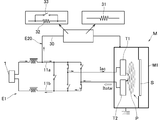
- the power supply device E is opposed to the substrate S to be processed in the vacuum chamber M1 of the sputtering device M, and supplies AC pulse power at a predetermined frequency to a pair of targets T1 and T2 that are electrodes in contact with plasma. Used to input (output).
- the power supply device E is a control means C that performs overall control of the first discharge circuit E1 and the second discharge circuit E2, and the operation of switching elements described later provided in the first discharge circuit E1 and the second discharge circuit E2. (See FIG. 1).
- the first discharge circuit E1 includes a DC power supply source 1 that enables supply of DC power.
- the DC power supply source 1 is a rectifier composed of, for example, an input unit to which commercial AC power (three-phase AC 200 V or 400 V) is input, and a diode that rectifies the input AC power and converts it into DC power. And outputs DC power to the oscillating unit via positive and negative DC power lines 11a and 11b.
- a switching transistor controlled by the control means 3 via an output oscillation driver circuit (not shown) is provided between the DC power lines 11a and 11b, so that supply of DC power to the oscillation unit can be controlled. ing.
- the oscillating unit includes a bridge circuit 12 including four first to fourth switching transistors (switching elements) SW11 to SW14 connected between positive and negative DC power lines 11a and 11b, and outputs from the bridge circuit 12 Lines 13a and 13b are connected to a pair of targets T1 and T2, respectively.
- the switching on / off of each of the switching transistors SW11 to SW14 is controlled by the control means C via an output oscillation driver circuit (not shown).
- the first and fourth switching transistors SW11, SW14 The switching of each of the switching transistors SW11 to SW14 is controlled so that the on / off timing of the third switching transistors SW12 and SW13 is reversed, and a predetermined frequency (for example, 1 to 10 kHz) is applied to the pair of targets T1 and T2. Then, a predetermined pulse potential is applied (output) with alternating polarity.
- a predetermined frequency for example, 1 to 10 kHz
- switching transistors SW11 to SW14 are switched in a state in which DC power is output from the DC power supply source 1, their switching loss becomes great, and thus the durability of the switching transistors SW11 to SW14 is improved. It is necessary to configure as follows. Therefore, switching between on and off is controlled between the positive and negative DC output lines 11a and 11b from the DC power supply source 1 by the control means C via an output oscillation driver circuit (not shown). A transistor SW15 is provided.
- the switching transistors SW11 to SW14 of the bridge circuit 12 are switched in a short-circuited state of the output short-circuiting switch transistor SW15 (a state where the output to the targets T1 and T2 is shut off) (FIG. 2). That is, when the switching transistor SW15 is short-circuited (on), for example, the first and fourth switching transistors SW11 and SW14 are turned on, and then the switching transistor SW15 is released (off) and output to one target T1. (A negative pulse potential is applied to the target T1). Next, the switching transistor SW15 is short-circuited again, the first and fourth switching transistors SW11 and SW14 are turned off, the second and third switching transistors SW12 and SW13 are turned on, and then the switching transistor SW15 is turned off. Output to the other target T2 (a negative pulse potential is applied to the target T2).
- the switching loss that occurs when outputting to the targets T1 and T2 occurs only in the switching transistor SW15, and almost no switching loss occurs in each of the switching transistors SW11 to SW14.
- high durability can be achieved without using a high-performance switching element, and a sufficient heat dissipation mechanism is not required as in the case where switching loss occurs with four switching elements, resulting in lower costs. I can plan. *
- the second discharge circuit E2 includes a DC power supply source 2 having the same configuration as that of the first discharge circuit E1.
- the positive DC power line 21a from the DC power supply source 2 is connected to the vacuum chamber M1 grounded.
- the negative DC power line 21b from the DC power supply source 2 is branched and connected to the output lines 13a and 13b of the first discharge circuit E1, respectively.
- switching transistors SW21 and SW22 that are operated in conjunction with the switching transistors SW11 to SW14 of the bridge circuit 13 are provided on the branch lines 22a and 22b from the negative DC power line 21b, respectively (see FIG. 1). ).
- the switching of both the switching transistors SW21 and SW22 is controlled by the control means C via an output oscillation driver circuit (not shown).
- the first and fourth switching transistors SW11 and SW14 are turned on.
- the switching transistor SW21 is turned on, and predetermined power is input to the other target T2 by the second discharge circuit E2. (See FIG. 2).
- a gas such as Ar is introduced at a constant flow rate through a gas introduction means (not shown) while the inside of the vacuum chamber M1 is maintained at a predetermined degree of vacuum, and a pair is formed by the first and second discharge circuits E1 and E2.
- the first and fourth switching transistors SW11 and SW14 are turned on (in this case, the second and third switching transistors SW12, for example).
- the second The on / off timings of the switching transistors SW21 and SW22 of the discharge circuit E2 are also inverted and output to the pair of targets T1 and T2 at a predetermined frequency.
- the targets T1 and T2 are alternately switched to the anode electrode and the cathode electrode, a glow discharge is generated between the anode electrode, the cathode electrode, the cathode electrode, and the ground, and a plasma atmosphere is formed. Sputtered.
- the power supply device E has a path through which the discharge current Idc flows between one target T1 or T2 and the ground in addition to a path through which the discharge current Iac flows between the pair of targets T1 and T2. .
- the plasma is biased only in front of the target being output when the output frequency is low, whereas In the power supply device E of the present embodiment, plasma P is generated in front of both targets T1 and T2 (see FIG. 1).
- a predetermined thin film is formed on the surface of the substrate S, it is easy to make the film thickness distribution uniform.
- a switching transistor SW23 for output short-circuiting is provided between the positive and negative DC power lines 21a and 21b, and outputs to the targets T1 and T2 similarly to the first discharge circuit E1. It is preferable that the switching loss generated at the time is generated only in the switching transistor SW23.
- the positive DC power line 21a is provided with a diode 24 with the ground side as a cathode.
- the capacitance component (capacitance) component is dominant over the inductance component. If the capacitive component is dominant in this way, the impedance on the plasma load side becomes small when arc discharge occurs, and the output and the plasma load are combined and suddenly released from the capacitive component to the output side.
- the positive and negative DC output lines 11a, 11b and 21a, 21b of the first and second discharge circuits E1, E2 are provided with the inductor 3 having an inductance value larger than the plasma inductance value, and a unit when arc discharge occurs.
- the rate of current increase per hour was limited.
- a diode 4 and a resistor 5 are provided in parallel to the inductor 3 and connected to each other in series. Yes.
- the switching transistors SW11 to SW14 and SW21, SW22 are switched (during polarity reversal) in the first and second discharge circuits E1, E2, the outputs to the targets T1, T2 are initially constant voltage specific. Then, the output current gradually increases, and after that (when the output current reaches a predetermined value), the output becomes a constant current characteristic.
- the inductor 3, the diode 4 and the resistor 5 are provided on the positive and negative DC output lines 11a, 11b and 21a, 21b, respectively, but any one of the DC output lines 11a, 11b and 21a, 21b is provided. You may make it provide in.
- the second discharge circuit E2 has the DC power supply source 2 different from the first discharge circuit E1.
- the present invention is not limited to this.
- the second discharge circuit E20 according to the modification is obtained by branching the positive DC output 11a from the DC power supply source 1 of the first discharge circuit E1 and grounding it. Yes, it may be configured by a resistor 31 provided on the branch line 30 or a device (branch circuit) having a switching element 33 connected in parallel with the resistor 32 on the branch line 30.
- the resistance values of the resistors 31 and 32 are appropriately selected according to the electric power to be input by the first discharge circuit E1 when a thin film is formed using the sputtering apparatus M.
- the circuit configuration of the power supply device E is simplified, and the number of parts is reduced, so that the cost can be reduced.
- a power supply device E having the same structure is assigned to each pair of targets of a plurality of same-shaped targets arranged in parallel at equal intervals so as to face the substrate S in the vacuum chamber, and an AC pulse is applied to each target at a predetermined frequency.
- the present invention can also be applied to a device to which a potential is applied, and the power supply device E of the present invention can also be applied to a case where a plurality of AC power supplies output to a pair of targets.
- the figure which shows the structure of the alternating current power supply of this invention roughly.
Landscapes
- Chemical & Material Sciences (AREA)
- Engineering & Computer Science (AREA)
- Physics & Mathematics (AREA)
- Plasma & Fusion (AREA)
- Organic Chemistry (AREA)
- Chemical Kinetics & Catalysis (AREA)
- Materials Engineering (AREA)
- Mechanical Engineering (AREA)
- Metallurgy (AREA)
- Analytical Chemistry (AREA)
- Spectroscopy & Molecular Physics (AREA)
- Electromagnetism (AREA)
- Power Engineering (AREA)
- Physical Vapour Deposition (AREA)
- Plasma Technology (AREA)
- Inverter Devices (AREA)
Priority Applications (3)
| Application Number | Priority Date | Filing Date | Title |
|---|---|---|---|
| KR1020117002276A KR101298167B1 (ko) | 2008-06-30 | 2009-06-17 | 전원 장치 |
| US13/001,454 US9210788B2 (en) | 2008-06-30 | 2009-06-17 | Power supply apparatus |
| CN2009801254002A CN102084024B (zh) | 2008-06-30 | 2009-06-17 | 电源装置 |
Applications Claiming Priority (2)
| Application Number | Priority Date | Filing Date | Title |
|---|---|---|---|
| JP2008-170806 | 2008-06-30 | ||
| JP2008170806A JP5429772B2 (ja) | 2008-06-30 | 2008-06-30 | 電源装置 |
Publications (1)
| Publication Number | Publication Date |
|---|---|
| WO2010001723A1 true WO2010001723A1 (ja) | 2010-01-07 |
Family
ID=41465824
Family Applications (1)
| Application Number | Title | Priority Date | Filing Date |
|---|---|---|---|
| PCT/JP2009/060988 WO2010001723A1 (ja) | 2008-06-30 | 2009-06-17 | 電源装置 |
Country Status (6)
| Country | Link |
|---|---|
| US (1) | US9210788B2 (de) |
| JP (1) | JP5429772B2 (de) |
| KR (1) | KR101298167B1 (de) |
| CN (1) | CN102084024B (de) |
| TW (1) | TWI500799B (de) |
| WO (1) | WO2010001723A1 (de) |
Cited By (1)
| Publication number | Priority date | Publication date | Assignee | Title |
|---|---|---|---|---|
| JP2015536386A (ja) * | 2012-11-01 | 2015-12-21 | エーリコン・サーフェス・ソリューションズ・アーゲー・トリューバッハ | 定形逐次電力分配用の電力分配器 |
Families Citing this family (24)
| Publication number | Priority date | Publication date | Assignee | Title |
|---|---|---|---|---|
| KR102038649B1 (ko) * | 2012-02-20 | 2019-10-30 | 도쿄엘렉트론가부시키가이샤 | 전원 시스템, 플라즈마 에칭 장치 및 플라즈마 에칭 방법 |
| KR102222902B1 (ko) * | 2014-05-12 | 2021-03-05 | 삼성전자주식회사 | 플라즈마 장비 및 이를 이용한 반도체 소자의 제조 방법 |
| DE102016012460A1 (de) * | 2016-10-19 | 2018-04-19 | Grenzebach Maschinenbau Gmbh | Vorrichtung und Verfahren zur Herstellung definierter Eigenschaften von Gradientenschichten in einem System mehrlagiger Beschichtungen bei Sputter - Anlagen |
| US10510575B2 (en) * | 2017-09-20 | 2019-12-17 | Applied Materials, Inc. | Substrate support with multiple embedded electrodes |
| US10555412B2 (en) | 2018-05-10 | 2020-02-04 | Applied Materials, Inc. | Method of controlling ion energy distribution using a pulse generator with a current-return output stage |
| US11476145B2 (en) | 2018-11-20 | 2022-10-18 | Applied Materials, Inc. | Automatic ESC bias compensation when using pulsed DC bias |
| CN113169026B (zh) | 2019-01-22 | 2024-04-26 | 应用材料公司 | 用于控制脉冲电压波形的反馈回路 |
| US11508554B2 (en) | 2019-01-24 | 2022-11-22 | Applied Materials, Inc. | High voltage filter assembly |
| CN109811324B (zh) * | 2019-03-14 | 2021-02-09 | 哈尔滨工业大学 | 基于异质双靶高功率脉冲磁控溅射制备掺杂类薄膜的装置及方法 |
| TWI692921B (zh) * | 2019-06-26 | 2020-05-01 | 台達電子工業股份有限公司 | 電源供應電路與操作方法 |
| US11462388B2 (en) | 2020-07-31 | 2022-10-04 | Applied Materials, Inc. | Plasma processing assembly using pulsed-voltage and radio-frequency power |
| US11901157B2 (en) | 2020-11-16 | 2024-02-13 | Applied Materials, Inc. | Apparatus and methods for controlling ion energy distribution |
| US11798790B2 (en) | 2020-11-16 | 2023-10-24 | Applied Materials, Inc. | Apparatus and methods for controlling ion energy distribution |
| US11495470B1 (en) | 2021-04-16 | 2022-11-08 | Applied Materials, Inc. | Method of enhancing etching selectivity using a pulsed plasma |
| US11791138B2 (en) | 2021-05-12 | 2023-10-17 | Applied Materials, Inc. | Automatic electrostatic chuck bias compensation during plasma processing |
| US11948780B2 (en) | 2021-05-12 | 2024-04-02 | Applied Materials, Inc. | Automatic electrostatic chuck bias compensation during plasma processing |
| US11967483B2 (en) | 2021-06-02 | 2024-04-23 | Applied Materials, Inc. | Plasma excitation with ion energy control |
| US20220399185A1 (en) | 2021-06-09 | 2022-12-15 | Applied Materials, Inc. | Plasma chamber and chamber component cleaning methods |
| US11810760B2 (en) | 2021-06-16 | 2023-11-07 | Applied Materials, Inc. | Apparatus and method of ion current compensation |
| US11569066B2 (en) | 2021-06-23 | 2023-01-31 | Applied Materials, Inc. | Pulsed voltage source for plasma processing applications |
| US11776788B2 (en) | 2021-06-28 | 2023-10-03 | Applied Materials, Inc. | Pulsed voltage boost for substrate processing |
| US11476090B1 (en) | 2021-08-24 | 2022-10-18 | Applied Materials, Inc. | Voltage pulse time-domain multiplexing |
| US11694876B2 (en) | 2021-12-08 | 2023-07-04 | Applied Materials, Inc. | Apparatus and method for delivering a plurality of waveform signals during plasma processing |
| US11972924B2 (en) | 2022-06-08 | 2024-04-30 | Applied Materials, Inc. | Pulsed voltage source for plasma processing applications |
Citations (6)
| Publication number | Priority date | Publication date | Assignee | Title |
|---|---|---|---|---|
| JPH02243762A (ja) * | 1989-03-17 | 1990-09-27 | Hitachi Ltd | スパッタ装置 |
| JPH10152772A (ja) * | 1996-11-22 | 1998-06-09 | Matsushita Electric Ind Co Ltd | スパッタリング方法及び装置 |
| JP2006299412A (ja) * | 2005-03-25 | 2006-11-02 | Bridgestone Corp | In−Ga−Zn−O膜の成膜方法 |
| JP2007186724A (ja) * | 2006-01-11 | 2007-07-26 | Ulvac Japan Ltd | スパッタリング方法及びスパッタリング装置 |
| JP2007186726A (ja) * | 2006-01-11 | 2007-07-26 | Ulvac Japan Ltd | スパッタリング装置 |
| JP2008138263A (ja) * | 2006-12-04 | 2008-06-19 | Toppan Printing Co Ltd | ロール・ツー・ロール型のマグネトロン・スパッタ装置、積層体、光学機能性フィルタ、及び光学表示装置 |
Family Cites Families (15)
| Publication number | Priority date | Publication date | Assignee | Title |
|---|---|---|---|---|
| US4597847A (en) * | 1984-10-09 | 1986-07-01 | Iodep, Inc. | Non-magnetic sputtering target |
| DE4042289A1 (de) * | 1990-12-31 | 1992-07-02 | Leybold Ag | Verfahren und vorrichtung zum reaktiven beschichten eines substrats |
| DE9109503U1 (de) | 1991-07-31 | 1991-10-17 | Magtron Magneto Elektronische Geraete Gmbh, 7583 Ottersweier, De | |
| DE4233720C2 (de) * | 1992-10-07 | 2001-05-17 | Leybold Ag | Einrichtung für die Verhinderung von Überschlägen in Vakuum-Zerstäubungsanlagen |
| US5681860A (en) * | 1993-09-21 | 1997-10-28 | The Trustees Of Columbia University In The City Of New York | Method of increasing expression of HLA, cell surface and TAA antigens of cells using 3-(N-acetylamino)-5-(N-decyl-N-methylamino)-benzyl alcohol |
| DE4446532A1 (de) * | 1994-12-24 | 1996-06-27 | Bosch Gmbh Robert | Stromversorgungsschaltung |
| US5584972A (en) * | 1995-02-01 | 1996-12-17 | Sony Corporation | Plasma noise and arcing suppressor apparatus and method for sputter deposition |
| DE19651811B4 (de) * | 1996-12-13 | 2006-08-31 | Unaxis Deutschland Holding Gmbh | Vorrichtung zum Belegen eines Substrats mit dünnen Schichten |
| JPH11146659A (ja) * | 1997-11-05 | 1999-05-28 | Haiden Kenkyusho:Kk | 正負パルス式スイッチング電源装置 |
| DE10018879B4 (de) * | 2000-04-17 | 2013-02-28 | Melec Gmbh | Stromversorgungsgerät zur bipolaren Stromversorgung |
| KR20040002796A (ko) * | 2002-06-28 | 2004-01-07 | 후지 샤신 필름 가부시기가이샤 | 편광판 점착방법 및 그 장치 |
| JP2005133110A (ja) | 2003-10-28 | 2005-05-26 | Konica Minolta Opto Inc | スパッタリング装置 |
| JP4780972B2 (ja) | 2004-03-11 | 2011-09-28 | 株式会社アルバック | スパッタリング装置 |
| JP4775948B2 (ja) * | 2005-11-17 | 2011-09-21 | 日東電工株式会社 | 光学表示装置の製造システム及びその製造方法 |
| TWI476289B (zh) * | 2006-12-12 | 2015-03-11 | Oerlikon Advanced Technologies Ag | 在高能脈衝磁管噴濺中之消弧及產生脈波 |
-
2008
- 2008-06-30 JP JP2008170806A patent/JP5429772B2/ja active Active
-
2009
- 2009-06-17 WO PCT/JP2009/060988 patent/WO2010001723A1/ja active Application Filing
- 2009-06-17 CN CN2009801254002A patent/CN102084024B/zh active Active
- 2009-06-17 KR KR1020117002276A patent/KR101298167B1/ko active IP Right Grant
- 2009-06-17 US US13/001,454 patent/US9210788B2/en active Active
- 2009-06-19 TW TW098120658A patent/TWI500799B/zh active
Patent Citations (6)
| Publication number | Priority date | Publication date | Assignee | Title |
|---|---|---|---|---|
| JPH02243762A (ja) * | 1989-03-17 | 1990-09-27 | Hitachi Ltd | スパッタ装置 |
| JPH10152772A (ja) * | 1996-11-22 | 1998-06-09 | Matsushita Electric Ind Co Ltd | スパッタリング方法及び装置 |
| JP2006299412A (ja) * | 2005-03-25 | 2006-11-02 | Bridgestone Corp | In−Ga−Zn−O膜の成膜方法 |
| JP2007186724A (ja) * | 2006-01-11 | 2007-07-26 | Ulvac Japan Ltd | スパッタリング方法及びスパッタリング装置 |
| JP2007186726A (ja) * | 2006-01-11 | 2007-07-26 | Ulvac Japan Ltd | スパッタリング装置 |
| JP2008138263A (ja) * | 2006-12-04 | 2008-06-19 | Toppan Printing Co Ltd | ロール・ツー・ロール型のマグネトロン・スパッタ装置、積層体、光学機能性フィルタ、及び光学表示装置 |
Cited By (2)
| Publication number | Priority date | Publication date | Assignee | Title |
|---|---|---|---|---|
| JP2015536386A (ja) * | 2012-11-01 | 2015-12-21 | エーリコン・サーフェス・ソリューションズ・アーゲー・トリューバッハ | 定形逐次電力分配用の電力分配器 |
| US10074976B2 (en) | 2012-11-01 | 2018-09-11 | Oerlikon Surface Solutions Ag, Pfäffikon | Power distributor for defined sequential power distribution |
Also Published As
| Publication number | Publication date |
|---|---|
| US9210788B2 (en) | 2015-12-08 |
| KR101298167B1 (ko) | 2013-08-21 |
| TW201006949A (en) | 2010-02-16 |
| JP5429772B2 (ja) | 2014-02-26 |
| CN102084024B (zh) | 2013-04-17 |
| US20110100807A1 (en) | 2011-05-05 |
| JP2010007161A (ja) | 2010-01-14 |
| TWI500799B (zh) | 2015-09-21 |
| CN102084024A (zh) | 2011-06-01 |
| KR20110025229A (ko) | 2011-03-09 |
Similar Documents
| Publication | Publication Date | Title |
|---|---|---|
| JP5429772B2 (ja) | 電源装置 | |
| KR101181875B1 (ko) | 바이폴라 펄스 전원 및 이 바이폴라 펄스 전원을 복수대 병렬 접속하여 구성되는 전원 장치 | |
| JP5124344B2 (ja) | バイポーラパルス電源及び複数のバイポーラパルス電源からなる電源装置並びに出力方法 | |
| JP5500794B2 (ja) | 電源装置 | |
| WO2009145093A1 (ja) | スパッタリング方法 | |
| JP2009284732A5 (de) | ||
| JP5186281B2 (ja) | バイポーラパルス電源及びこのバイポーラパルス電源を複数台並列接続してなる電源装置 | |
| TW201948020A (zh) | 降低裂紋的設備、系統和方法 | |
| TW201146093A (en) | Power supply apparatus | |
| TWI518194B (zh) | Sputtering method | |
| JP2013189698A (ja) | 成膜装置および成膜方法 | |
| JP2002241934A (ja) | スパッタ方法およびスパッタ装置 |
Legal Events
| Date | Code | Title | Description |
|---|---|---|---|
| WWE | Wipo information: entry into national phase |
Ref document number: 200980125400.2 Country of ref document: CN |
|
| 121 | Ep: the epo has been informed by wipo that ep was designated in this application |
Ref document number: 09773301 Country of ref document: EP Kind code of ref document: A1 |
|
| WWE | Wipo information: entry into national phase |
Ref document number: 13001454 Country of ref document: US |
|
| NENP | Non-entry into the national phase |
Ref country code: DE |
|
| ENP | Entry into the national phase |
Ref document number: 20117002276 Country of ref document: KR Kind code of ref document: A |
|
| 122 | Ep: pct application non-entry in european phase |
Ref document number: 09773301 Country of ref document: EP Kind code of ref document: A1 |