WO2009145196A1 - 半導体チップ、中間基板および半導体装置 - Google Patents
半導体チップ、中間基板および半導体装置 Download PDFInfo
- Publication number
- WO2009145196A1 WO2009145196A1 PCT/JP2009/059619 JP2009059619W WO2009145196A1 WO 2009145196 A1 WO2009145196 A1 WO 2009145196A1 JP 2009059619 W JP2009059619 W JP 2009059619W WO 2009145196 A1 WO2009145196 A1 WO 2009145196A1
- Authority
- WO
- WIPO (PCT)
- Prior art keywords
- wiring
- electrode
- semiconductor chip
- electrodes
- semiconductor
- Prior art date
- Legal status (The legal status is an assumption and is not a legal conclusion. Google has not performed a legal analysis and makes no representation as to the accuracy of the status listed.)
- Ceased
Links
Images










Classifications
-
- H—ELECTRICITY
- H10—SEMICONDUCTOR DEVICES; ELECTRIC SOLID-STATE DEVICES NOT OTHERWISE PROVIDED FOR
- H10W—GENERIC PACKAGES, INTERCONNECTIONS, CONNECTORS OR OTHER CONSTRUCTIONAL DETAILS OF DEVICES COVERED BY CLASS H10
- H10W74/00—Encapsulations, e.g. protective coatings
- H10W74/01—Manufacture or treatment
- H10W74/012—Manufacture or treatment of encapsulations on active surfaces of flip-chip devices, e.g. forming underfills
-
- H—ELECTRICITY
- H10—SEMICONDUCTOR DEVICES; ELECTRIC SOLID-STATE DEVICES NOT OTHERWISE PROVIDED FOR
- H10W—GENERIC PACKAGES, INTERCONNECTIONS, CONNECTORS OR OTHER CONSTRUCTIONAL DETAILS OF DEVICES COVERED BY CLASS H10
- H10W70/00—Package substrates; Interposers; Redistribution layers [RDL]
- H10W70/60—Insulating or insulated package substrates; Interposers; Redistribution layers
-
- H—ELECTRICITY
- H10—SEMICONDUCTOR DEVICES; ELECTRIC SOLID-STATE DEVICES NOT OTHERWISE PROVIDED FOR
- H10W—GENERIC PACKAGES, INTERCONNECTIONS, CONNECTORS OR OTHER CONSTRUCTIONAL DETAILS OF DEVICES COVERED BY CLASS H10
- H10W74/00—Encapsulations, e.g. protective coatings
- H10W74/10—Encapsulations, e.g. protective coatings characterised by their shape or disposition
- H10W74/111—Encapsulations, e.g. protective coatings characterised by their shape or disposition the semiconductor body being completely enclosed
- H10W74/114—Encapsulations, e.g. protective coatings characterised by their shape or disposition the semiconductor body being completely enclosed by a substrate and the encapsulations
- H10W74/117—Encapsulations, e.g. protective coatings characterised by their shape or disposition the semiconductor body being completely enclosed by a substrate and the encapsulations the substrate having spherical bumps for external connection
-
- H—ELECTRICITY
- H10—SEMICONDUCTOR DEVICES; ELECTRIC SOLID-STATE DEVICES NOT OTHERWISE PROVIDED FOR
- H10W—GENERIC PACKAGES, INTERCONNECTIONS, CONNECTORS OR OTHER CONSTRUCTIONAL DETAILS OF DEVICES COVERED BY CLASS H10
- H10W74/00—Encapsulations, e.g. protective coatings
- H10W74/10—Encapsulations, e.g. protective coatings characterised by their shape or disposition
- H10W74/111—Encapsulations, e.g. protective coatings characterised by their shape or disposition the semiconductor body being completely enclosed
- H10W74/129—Encapsulations, e.g. protective coatings characterised by their shape or disposition the semiconductor body being completely enclosed forming a chip-scale package [CSP]
-
- H—ELECTRICITY
- H10—SEMICONDUCTOR DEVICES; ELECTRIC SOLID-STATE DEVICES NOT OTHERWISE PROVIDED FOR
- H10W—GENERIC PACKAGES, INTERCONNECTIONS, CONNECTORS OR OTHER CONSTRUCTIONAL DETAILS OF DEVICES COVERED BY CLASS H10
- H10W74/00—Encapsulations, e.g. protective coatings
- H10W74/10—Encapsulations, e.g. protective coatings characterised by their shape or disposition
- H10W74/15—Encapsulations, e.g. protective coatings characterised by their shape or disposition on active surfaces of flip-chip devices, e.g. underfills
-
- H—ELECTRICITY
- H10—SEMICONDUCTOR DEVICES; ELECTRIC SOLID-STATE DEVICES NOT OTHERWISE PROVIDED FOR
- H10W—GENERIC PACKAGES, INTERCONNECTIONS, CONNECTORS OR OTHER CONSTRUCTIONAL DETAILS OF DEVICES COVERED BY CLASS H10
- H10W90/00—Package configurations
-
- H—ELECTRICITY
- H10—SEMICONDUCTOR DEVICES; ELECTRIC SOLID-STATE DEVICES NOT OTHERWISE PROVIDED FOR
- H10W—GENERIC PACKAGES, INTERCONNECTIONS, CONNECTORS OR OTHER CONSTRUCTIONAL DETAILS OF DEVICES COVERED BY CLASS H10
- H10W20/00—Interconnections in chips, wafers or substrates
- H10W20/40—Interconnections external to wafers or substrates, e.g. back-end-of-line [BEOL] metallisations or vias connecting to gate electrodes
- H10W20/49—Adaptable interconnections, e.g. fuses or antifuses
-
- H—ELECTRICITY
- H10—SEMICONDUCTOR DEVICES; ELECTRIC SOLID-STATE DEVICES NOT OTHERWISE PROVIDED FOR
- H10W—GENERIC PACKAGES, INTERCONNECTIONS, CONNECTORS OR OTHER CONSTRUCTIONAL DETAILS OF DEVICES COVERED BY CLASS H10
- H10W72/00—Interconnections or connectors in packages
- H10W72/20—Bump connectors, e.g. solder bumps or copper pillars; Dummy bumps; Thermal bumps
-
- H—ELECTRICITY
- H10—SEMICONDUCTOR DEVICES; ELECTRIC SOLID-STATE DEVICES NOT OTHERWISE PROVIDED FOR
- H10W—GENERIC PACKAGES, INTERCONNECTIONS, CONNECTORS OR OTHER CONSTRUCTIONAL DETAILS OF DEVICES COVERED BY CLASS H10
- H10W72/00—Interconnections or connectors in packages
- H10W72/20—Bump connectors, e.g. solder bumps or copper pillars; Dummy bumps; Thermal bumps
- H10W72/241—Dispositions, e.g. layouts
- H10W72/242—Dispositions, e.g. layouts relative to the surface, e.g. recessed, protruding
-
- H—ELECTRICITY
- H10—SEMICONDUCTOR DEVICES; ELECTRIC SOLID-STATE DEVICES NOT OTHERWISE PROVIDED FOR
- H10W—GENERIC PACKAGES, INTERCONNECTIONS, CONNECTORS OR OTHER CONSTRUCTIONAL DETAILS OF DEVICES COVERED BY CLASS H10
- H10W72/00—Interconnections or connectors in packages
- H10W72/20—Bump connectors, e.g. solder bumps or copper pillars; Dummy bumps; Thermal bumps
- H10W72/29—Bond pads specially adapted therefor
-
- H—ELECTRICITY
- H10—SEMICONDUCTOR DEVICES; ELECTRIC SOLID-STATE DEVICES NOT OTHERWISE PROVIDED FOR
- H10W—GENERIC PACKAGES, INTERCONNECTIONS, CONNECTORS OR OTHER CONSTRUCTIONAL DETAILS OF DEVICES COVERED BY CLASS H10
- H10W72/00—Interconnections or connectors in packages
- H10W72/50—Bond wires
- H10W72/551—Materials of bond wires
- H10W72/552—Materials of bond wires comprising metals or metalloids, e.g. silver
- H10W72/5522—Materials of bond wires comprising metals or metalloids, e.g. silver comprising gold [Au]
-
- H—ELECTRICITY
- H10—SEMICONDUCTOR DEVICES; ELECTRIC SOLID-STATE DEVICES NOT OTHERWISE PROVIDED FOR
- H10W—GENERIC PACKAGES, INTERCONNECTIONS, CONNECTORS OR OTHER CONSTRUCTIONAL DETAILS OF DEVICES COVERED BY CLASS H10
- H10W72/00—Interconnections or connectors in packages
- H10W72/50—Bond wires
- H10W72/59—Bond pads specially adapted therefor
-
- H—ELECTRICITY
- H10—SEMICONDUCTOR DEVICES; ELECTRIC SOLID-STATE DEVICES NOT OTHERWISE PROVIDED FOR
- H10W—GENERIC PACKAGES, INTERCONNECTIONS, CONNECTORS OR OTHER CONSTRUCTIONAL DETAILS OF DEVICES COVERED BY CLASS H10
- H10W72/00—Interconnections or connectors in packages
- H10W72/851—Dispositions of multiple connectors or interconnections
- H10W72/853—On the same surface
- H10W72/856—Bump connectors and die-attach connectors
-
- H—ELECTRICITY
- H10—SEMICONDUCTOR DEVICES; ELECTRIC SOLID-STATE DEVICES NOT OTHERWISE PROVIDED FOR
- H10W—GENERIC PACKAGES, INTERCONNECTIONS, CONNECTORS OR OTHER CONSTRUCTIONAL DETAILS OF DEVICES COVERED BY CLASS H10
- H10W72/00—Interconnections or connectors in packages
- H10W72/851—Dispositions of multiple connectors or interconnections
- H10W72/874—On different surfaces
- H10W72/884—Die-attach connectors and bond wires
-
- H—ELECTRICITY
- H10—SEMICONDUCTOR DEVICES; ELECTRIC SOLID-STATE DEVICES NOT OTHERWISE PROVIDED FOR
- H10W—GENERIC PACKAGES, INTERCONNECTIONS, CONNECTORS OR OTHER CONSTRUCTIONAL DETAILS OF DEVICES COVERED BY CLASS H10
- H10W72/00—Interconnections or connectors in packages
- H10W72/90—Bond pads, in general
- H10W72/931—Shapes of bond pads
- H10W72/932—Plan-view shape, i.e. in top view
-
- H—ELECTRICITY
- H10—SEMICONDUCTOR DEVICES; ELECTRIC SOLID-STATE DEVICES NOT OTHERWISE PROVIDED FOR
- H10W—GENERIC PACKAGES, INTERCONNECTIONS, CONNECTORS OR OTHER CONSTRUCTIONAL DETAILS OF DEVICES COVERED BY CLASS H10
- H10W72/00—Interconnections or connectors in packages
- H10W72/90—Bond pads, in general
- H10W72/941—Dispositions of bond pads
- H10W72/9415—Dispositions of bond pads relative to the surface, e.g. recessed, protruding
-
- H—ELECTRICITY
- H10—SEMICONDUCTOR DEVICES; ELECTRIC SOLID-STATE DEVICES NOT OTHERWISE PROVIDED FOR
- H10W—GENERIC PACKAGES, INTERCONNECTIONS, CONNECTORS OR OTHER CONSTRUCTIONAL DETAILS OF DEVICES COVERED BY CLASS H10
- H10W74/00—Encapsulations, e.g. protective coatings
-
- H—ELECTRICITY
- H10—SEMICONDUCTOR DEVICES; ELECTRIC SOLID-STATE DEVICES NOT OTHERWISE PROVIDED FOR
- H10W—GENERIC PACKAGES, INTERCONNECTIONS, CONNECTORS OR OTHER CONSTRUCTIONAL DETAILS OF DEVICES COVERED BY CLASS H10
- H10W90/00—Package configurations
- H10W90/701—Package configurations characterised by the relative positions of pads or connectors relative to package parts
- H10W90/721—Package configurations characterised by the relative positions of pads or connectors relative to package parts of bump connectors
- H10W90/722—Package configurations characterised by the relative positions of pads or connectors relative to package parts of bump connectors between stacked chips
-
- H—ELECTRICITY
- H10—SEMICONDUCTOR DEVICES; ELECTRIC SOLID-STATE DEVICES NOT OTHERWISE PROVIDED FOR
- H10W—GENERIC PACKAGES, INTERCONNECTIONS, CONNECTORS OR OTHER CONSTRUCTIONAL DETAILS OF DEVICES COVERED BY CLASS H10
- H10W90/00—Package configurations
- H10W90/701—Package configurations characterised by the relative positions of pads or connectors relative to package parts
- H10W90/721—Package configurations characterised by the relative positions of pads or connectors relative to package parts of bump connectors
- H10W90/724—Package configurations characterised by the relative positions of pads or connectors relative to package parts of bump connectors between a chip and a stacked insulating package substrate, interposer or RDL
-
- H—ELECTRICITY
- H10—SEMICONDUCTOR DEVICES; ELECTRIC SOLID-STATE DEVICES NOT OTHERWISE PROVIDED FOR
- H10W—GENERIC PACKAGES, INTERCONNECTIONS, CONNECTORS OR OTHER CONSTRUCTIONAL DETAILS OF DEVICES COVERED BY CLASS H10
- H10W90/00—Package configurations
- H10W90/701—Package configurations characterised by the relative positions of pads or connectors relative to package parts
- H10W90/731—Package configurations characterised by the relative positions of pads or connectors relative to package parts of die-attach connectors
- H10W90/732—Package configurations characterised by the relative positions of pads or connectors relative to package parts of die-attach connectors between stacked chips
-
- H—ELECTRICITY
- H10—SEMICONDUCTOR DEVICES; ELECTRIC SOLID-STATE DEVICES NOT OTHERWISE PROVIDED FOR
- H10W—GENERIC PACKAGES, INTERCONNECTIONS, CONNECTORS OR OTHER CONSTRUCTIONAL DETAILS OF DEVICES COVERED BY CLASS H10
- H10W90/00—Package configurations
- H10W90/701—Package configurations characterised by the relative positions of pads or connectors relative to package parts
- H10W90/731—Package configurations characterised by the relative positions of pads or connectors relative to package parts of die-attach connectors
- H10W90/734—Package configurations characterised by the relative positions of pads or connectors relative to package parts of die-attach connectors between a chip and a stacked insulating package substrate, interposer or RDL
-
- H—ELECTRICITY
- H10—SEMICONDUCTOR DEVICES; ELECTRIC SOLID-STATE DEVICES NOT OTHERWISE PROVIDED FOR
- H10W—GENERIC PACKAGES, INTERCONNECTIONS, CONNECTORS OR OTHER CONSTRUCTIONAL DETAILS OF DEVICES COVERED BY CLASS H10
- H10W90/00—Package configurations
- H10W90/701—Package configurations characterised by the relative positions of pads or connectors relative to package parts
- H10W90/751—Package configurations characterised by the relative positions of pads or connectors relative to package parts of bond wires
- H10W90/754—Package configurations characterised by the relative positions of pads or connectors relative to package parts of bond wires between a chip and a stacked insulating package substrate, interposer or RDL
Definitions
- the present invention relates to a semiconductor chip and a semiconductor device on which the semiconductor chip is mounted, and more particularly to a technique that is effective when applied to a semiconductor device having a structure in which the semiconductor chip is mounted on a substrate or another chip by solder bumps.
- connection part by the solder bump is generally more reliable than the connection part by the Au bump. That is, in the connection part by the Au bump, the Au bump itself can be softly deformed. For example, when the Au bump is connected by melting a solder layer formed in advance on the substrate electrode, the hard and brittle AuSn is formed. Since the compound precipitates at the connection part, if the stress caused by the change of heat during actual use or the stress caused by the difference in thermal expansion coefficient between materials becomes large, these stresses cannot be absorbed by the connection part. , Cracks occur, leading to breakage. As a method that does not involve a solder layer, it is possible to directly connect Au bumps to Au plated substrate electrodes by ultrasonic connection, thermocompression bonding, etc., but it may be difficult to ensure interface strength and to cope with narrow pitch. .
- solder bumps when solder bumps are used, the compound is mainly generated only at the electrode interface, and the inside of the connection portion is composed of a solder component.
- Solder has various compositions, but conventional Sn-Pb solder, Pb-free solder Sn-based, Sn-Ag-based, Sn-Cu-based, Sn-Ag-Cu-based solder can be plastically deformed and used It is possible to absorb the stress caused by the heat of time, the stress caused by the coefficient of thermal expansion between the materials, etc., by the deformation of the structure in the solder. For this reason, the reliability of the connecting portion is high, and it is often used for semiconductor devices used in automobile equipment and the like in which shock and vibration are particularly important problems.
- solder bumps Another reason for using solder bumps is that when the number of pins of a semiconductor chip is required due to further enhancement of the functionality of electronic equipment, the use of Au bumps on electrodes by Al pads arranged around the chip, Since the necessary number of pins must be secured on the outer periphery, the chip area increases. In the case of a portable electronic device, it is important to be small and thin, and a semiconductor chip used inside is also required to be small and thin. For this reason, even if the number of electrodes is increased due to higher functionality, an increase in chip area is not allowed. Therefore, it is necessary to narrow the pitch between the electrodes, but there is a manufacturing limit in narrowing the pitch.
- WLP Wafer Level Package
- WPP WPP
- rewiring is performed on the chip using Cu or the like from the electrode by the Al pad around the chip, the electrode is drawn out over the entire chip area, and solder bumps are formed on this electrode.
- a semiconductor chip structure called “Wafer Process Package” or the like is used (for example, Patent Document 1).
- the electrodes after the rewiring may be arranged over the entire chip area or may be arranged in several rows around the chip due to the routing of the counterpart substrate electrode.
- solder bumps on each redistributed electrode such as plating using a resist, solder ball mounting and melting, and solder paste printing.
- the solder bump height and composition are easy to form.
- the thickness of the chip has been reduced due to the demand for thinner portable electronic devices.
- chips having a thickness of 200 ⁇ m or less have been put into practical use, but it is possible to reduce the thickness to about 20 ⁇ m in research and development.
- the substrate on which the semiconductor chip is mounted is often connected to a mother substrate of the apparatus body, and is called an intermediate substrate, an interposer substrate, etc., and a conductor wiring layer and an interlayer insulating resin layer are laminated,
- a printed wiring board is used in which a plurality of electrodes are formed on one or both outermost surfaces by the conductor wiring layer, and the other is covered with a surface insulating resin layer.
- a wiring made of Cu is usually formed on the surface of a core layer made of an insulating resin material, an interlayer insulating resin layer is formed on the surface, and upper and lower wirings are connected by through holes.
- a printed wiring board (a so-called build-up substrate) in which a wiring layer of a necessary number of layers is formed by repeating a process of forming a conductor wiring layer of Cu usually on the layer is used.
- the conductor wiring layer is usually Cu
- the electrode formed on the outermost surface is Cu, an organic layer as a surface protective film on Cu, or a Ni layer on Cu to improve wettability
- the structure is such that an Au layer is formed on the surface, or an Au layer is formed on Cu, or an Ni layer is formed on Cu, a Pd layer is formed on the surface, and an Au layer is formed on the surface.
- a solder resist is usually used for the surface insulating resin layer in order to prevent bridging between adjacent solder bumps and to protect the surface wiring layer other than the electrodes.
- the semiconductor chip when connecting a semiconductor chip by solder bumps, if the semiconductor chip is thick, it is mounted in alignment with the mating substrate electrode or chip electrode and heated by a reflow furnace. Then, the solder can be melted and connected to the substrate electrode or the chip electrode.
- the surface stress is different between the surface where the device is formed and the surface where the device is not formed, and the chip is warped.
- the warpage is about 2 mm when the wafer thickness is 400 ⁇ m, but the warpage at 200 ⁇ m is about 10 mm and 100 ⁇ m.
- the thickness is about 50 mm and 50 ⁇ m, the wafer becomes round, and the amount of warpage increases as the thickness becomes thinner. Therefore, in the case of a thin semiconductor chip, even if it is aligned and heated in a reflow furnace to sufficiently melt the solder bump, it does not come into contact with the mating substrate electrode or chip electrode, making connection impossible.
- thermocompression bonding it is conceivable to use a method in which a thin semiconductor chip is vacuum-adsorbed on a flat tool to eliminate warpage, align with the other substrate electrode and chip electrode, and connect by thermocompression bonding.
- a method in which a thin semiconductor chip is vacuum-adsorbed on a flat tool to eliminate warpage, align with the other substrate electrode and chip electrode, and connect by thermocompression bonding.
- thermocompression bonding For example, using a flip chip bonder, vacuum bonding a thin chip to a flat bonding head, aligning it, supplying heat from the bonding head, and melting solder bumps can be used as substrate electrodes or chip electrodes. Press to make contact and solder. Thereby, even a thin semiconductor chip can be connected without a problem of warping.
- the problem here is that when pressurizing molten solder bumps, the molten solder is a liquid, so the solder bumps are easily deformed and easily collapsed, and adjacent bumps come into contact with each other to form a solder bridge, etc. It occurs. Therefore, when solder bumps are thermocompression bonded, it is required to control with low load so as not to bridge.
- preheating can also be performed, and it is possible to suppress heat distribution due to a difference in heat conduction between the chip, the substrate, and the like.
- the present invention solves these problems, and is a thin semiconductor chip having solder bumps, and even if the wiring shape varies from electrode to electrode, thermocompression bonding is performed in a short time with a high yield, and a highly reliable connection portion.
- the present invention provides a semiconductor device intended to form a semiconductor device.
- the present invention solves these problems, and even with a printed wiring board having a plurality of electrodes, even when the wiring shape and the surrounding wiring structure are different for each electrode, thermocompression bonding is performed in a short time with a high yield.
- a semiconductor device for the purpose of forming a reliable connection portion is provided.
- the outline of a representative one is that a plurality of electrodes formed on the first electrode among a plurality of electrodes connected to a circuit formed in an element formation layer on a semiconductor substrate are formed one by one on each of the plurality of electrodes.
- Heat conduction wiring is connected to reduce the difference in the melting state of the solder bumps (ideally to make the solder bump melting state uniform), and the heat conduction wiring is formed by rewiring. It is characterized by that. Specifically, when the electrodes are formed on the whole or part of the chip area by rewiring from the peripheral Al pad electrodes on the device surface of the semiconductor chip, the lead-out wiring of each electrode is only meant as electrical wiring.
- the electrode structure is provided with a dummy wiring as the heat conduction wiring so that the heat supply amount is uniform to some extent.
- the dummy wiring at this time may be only one direction in a direction that does not affect the electrical signal, but may be formed in any direction.
- dummy wires may be provided in order to make the molten state of the solder uniform even with electrodes having ground wires, power supply wires, and signal wires.
- the plurality of electrodes on the surface of the substrate corresponding to the semiconductor chip have a structure in which heat conductive wiring for making the temperature of the electrodes uniform when connected is formed.
- the structure in which the heat conduction wiring is formed immediately below the surface insulating resin layer in contact with the electrode, and the shape of the heat conduction wiring are different structures depending on the heat distribution of the electrode.
- dummy wirings may be provided in one direction or in several directions on the surface layer.
- either or both of the semiconductor chip that has been subjected to temperature uniformity and the substrate that has been subjected to temperature uniformity are used.
- a thin semiconductor chip having solder bumps which can be thermocompression bonded in a short time with a high yield and has a highly reliable connection even when the wiring shape varies from electrode to electrode. can do.
- thermocompression bonding with high yield in a short time even on substrates having different wiring shapes for each electrode.
- a semiconductor device having a highly reliable connection portion can be provided by using a semiconductor chip or a substrate with improved thermal uniformity as described above, but by using both in combination, a shorter time and a higher yield can be provided. Can connect.
- the semiconductor chip of one embodiment of this invention it is a figure which shows the cross-section of WPP with a dummy wiring. It is a figure which shows another example of the electrode structure in which the dummy wiring was formed in the semiconductor chip of one embodiment of this invention. It is a figure which shows another example of the electrode structure in which the dummy wiring was formed in the semiconductor chip of one embodiment of this invention. It is a figure which shows the flip chip BGA which is a semiconductor device which mounted the semiconductor chip of one embodiment of this invention. It is a figure which shows the package of the CoC structure which is a semiconductor device which mounted the semiconductor chip of one embodiment of this invention.
- FIG. 1 It is a figure which shows the electrode structure which formed the dummy wiring in the package of the CoC structure which is a semiconductor device which mounted the semiconductor chip of one embodiment of this invention.
- the semiconductor device which mounted the semiconductor chip of one embodiment of this invention it is a figure which shows the structure of the connection part in the thermocompression bonding process of a semiconductor chip.
- the semiconductor device which mounted the semiconductor chip of one embodiment of this invention it is a figure which shows another electrode structure in which the dummy wiring was formed in the semiconductor device which mounted the semiconductor chip of one embodiment of this invention.
- FIG. 6 is a view showing the vicinity of an interface with a substrate electrode at a connection portion of an outermost solder bump in a conventional substrate.
- FIG. 6 is a view showing the vicinity of the interface with the substrate electrode at the connection portion of the third solder bump from the outermost periphery in the substrate of the prior art.
- 1 is a diagram showing an electrode structure in which dummy through holes are formed in a substrate electrode in a semiconductor device using a substrate according to an embodiment of the present invention. In the semiconductor device using the board
- FIG. 1 is a diagram showing an electrode structure in which dummy wirings are formed on a surface layer of a substrate electrode in a semiconductor device using a substrate according to an embodiment of the present invention. It is a figure which shows the wiring structure in case there is no extraction wiring in the semiconductor chip of a prior art. It is a figure which shows the wiring structure with wiring for signals in the semiconductor chip of a prior art. It is a figure which shows the wiring structure connected with the wiring for power supplies, or the ground wiring in the semiconductor chip of a prior art.
- the semiconductor device is a WLP in which rewiring is performed on a chip using Cu or the like from an electrode formed by an Al pad around the chip, an electrode is drawn out over the entire chip area, and a solder bump is formed on the electrode.
- a semiconductor chip structure called WPP or the like is used.
- the electrodes after the rewiring may be arranged over the entire chip area or may be arranged in several rows around the chip due to the routing of the counterpart substrate electrode.
- a method is used in which a thin semiconductor chip is vacuum-adsorbed on a flat tool to eliminate warpage, align with the substrate electrode and chip electrode of the counterpart, and connect by thermocompression bonding.
- a flip chip bonder vacuum bonding a thin chip to a flat bonding head, aligning it, supplying heat from the bonding head, and melting solder bumps can be used as substrate electrodes or chip electrodes. Press to make contact and solder. Thereby, even a thin semiconductor chip can be connected without a problem of warping.
- the heat distribution differs depending on the wiring shape on the semiconductor chip due to the supply of heat from the back surface of the semiconductor chip during thermocompression bonding.
- the electrodes with ground wiring, power wiring, and signal wiring The temperature rises rapidly due to heat conduction, and the solder bumps are sufficiently heated and melted, and the fluidity of the solder is ensured and can be spread in a spherical shape.
- the temperature rise is slow and the solder bumps are not sufficiently heated, so that the melting is insufficient, the solder fluidity is low, the solder cannot spread in a spherical shape, and the surface oxide film It is thought that it became an irregular shape by the influence of.
- the void detachability in the solder bumps is reduced due to the decrease in the solder fluidity.
- shape change of the solder after thermocompression bonding was investigated in detail, it was found that the shape of the solder after thermocompression bonding was different when the wiring thickness was different between the ground wiring, the power supply wiring, and the signal wiring. The difference in the shape of these solders becomes more prominent when heat is not sufficiently applied during thermocompression bonding.
- a thin semiconductor chip having solder bumps is formed by thermocompression bonding at a high yield in a short time to form a highly reliable connection portion even when the wiring shape varies from electrode to electrode.
- FIGS. A semiconductor chip according to an embodiment of the present invention will be described with reference to FIGS.
- description will be made in comparison with the prior art.
- the present embodiment an example in which the present invention is applied to a semiconductor chip on which 432 solder bumps are formed at a pitch of 250 ⁇ m is shown.
- FIG. 2 shows the entire semiconductor chip of the present embodiment (same as the prior art).
- the semiconductor chip 10 has an Al pad 11 arranged in the periphery, and electrodes 12 made of solder bumps are formed in an area array on the semiconductor chip 10 by rewiring. Therefore, the pitch of the electrode 12 by the solder bump is wider than that of the Al pad 11, and the wiring of the board to be connected can be easily routed.
- a circuit is formed in an element formation layer on a semiconductor substrate, and electrodes 12 by solder bumps are formed on the surface of the element formation layer by rewiring.
- FIG. 3 shows a part of the rewiring of the semiconductor chip 10 of the prior art.
- electrodes 12 by solder bumps are arranged on the chip device surface by rewiring, and signal wirings 13, power supply wirings, or ground wirings 14 are drawn out from the respective electrodes.
- electrodes 15 that have no lead wires because of the relationship between the number of electrodes by the Al pads 11 around the semiconductor chip and the number of electrodes 12 by the solder bumps arranged in the center by rewiring.
- the solder bump array is more symmetrical and the subsequent underfill material injection and thermal fatigue reliability of the connection are higher, so an asymmetrical array structure in which the solder bumps are thinned to equalize the number of electrodes. This is because I don't want to take it.
- FIG. 4 shows the result of heating and pressing the solder bumps on the semiconductor chip 10.
- the heating and pressing conditions were such that the back of the chip device surface was brought into contact with a heater at 260 ° C., and a load of about 150 g was applied to the entire semiconductor chip 10 so that the solder bumps were crushed by about 40 ⁇ m.
- the atmosphere is in the air.
- the solder bumps of the electrodes connected to the signal wiring 13 and the solder bumps connected to the power supply wiring or the ground wiring 14 are round and spread almost uniformly around the periphery. Protrusions were formed around the solder bumps with no electrode 15 and spread in an irregular shape.
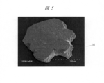
- solder bumps shown in FIG. 4 the result of observing the solder bumps 16 spreading in a crack by SEM is shown in FIG.
- the solder bumps 16 spreading in a distorted manner have a shape in which the solder is not spherical but has a sharp periphery. Further, as can be seen from FIG. 4, it is considered that the solder having an irregular color on the solder surface is brown and a lot of surface oxide film remains.
- the thermal conductivity differs depending on the shape of the lead-out wiring to the electrode of each solder bump, as shown in FIG. That is, when heated from the back of the chip device surface by the bonding head, the temperature rise rate differs for each solder bump, and the solder bump connected to the power supply wiring or ground wiring 14 is supplied with heat from the wiring and the melting point of the solder. Since it has sufficiently reached the above, the molten solder has high fluidity, good void detachability, can be spread around the circumference almost uniformly, and has high connection reliability.
- solder bump on the electrode 15 having no lead-out wiring could not secure a time longer than the melting point of the solder, so that the solder fluidity is low and it is considered that the solder bump spread around the periphery. If it spreads in an irregular shape, the probability of bridging with adjacent bumps increases, and the surface oxide film remains, resulting in low wettability, insufficient void detachment, and low connection reliability. It is predicted.
- the electrode connected to the power supply wiring or the ground wiring 14 has a large hole in the solder (the shading in FIG. 4). It is seen that the void has been removed), but a small hole was seen in the electrode connected to the signal wiring 13, but it was seen in the electrode connected to the power wiring or ground wiring 14. There wasn't enough holes. In the electrode 15 having no lead-out wiring, holes are not clearly seen, and it is considered that voids are not easily removed. Therefore, it is considered that there is a difference in the solder fluidity depending on the wiring shape from the electrode.
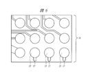
- a semiconductor chip as shown in FIG. 6 (showing part of the rewiring of the semiconductor chip) is used.
- a dummy wiring (heat conduction wiring) 17 is provided on the electrode 15 having no lead-out wiring, and the semiconductor chip 18 is provided with the dummy wiring.
- FIG. 1 Details of the electrode structure in which the dummy wiring 17 is formed are shown in FIG.
- a dummy wiring 17 is formed, and a surface layer 19 made of polyimide is formed on the surface around the electrode.
- the polyimide surface layer 19 defines an opening 20 to which a solder bump is connected, and the actual rewiring layer 21 extends to a circular dotted line.
- Solder bumps 22 are formed in the opening 20.
- FIG. 7 shows a cross-sectional structure of a conventional WPP.
- an Al pad 11 is formed around the semiconductor chip 10, and a passivation film 23 is formed on the surface.
- a polyimide layer 24 having an Al pad 11 portion opened is formed on the surface of the passivation film 23 .
- the polyimide layer 24 is formed by applying a photosensitive polyimide resin film over the entire surface, opening the Al pad 11 by heat treatment (pre-baking), exposure, and development, and then performing heat treatment to cure the polyimide resin film.
- a Cr / Cu film 26, a Cu film 27, and a Ni film 28 are formed as a rewiring layer 25 in a laminated structure.
- the rewiring layer 25 is formed by depositing Cr / Cu as a seed layer for electrolytic plating by sputtering, forming a resist layer having a rewiring groove on the seed layer by a photolithography technique. A Cu film 27 and then a Ni film 28 are formed only inside, and the resist layer and an unnecessary portion of the seed layer (Cr / Cu) are removed.
- solder bumps 22 are formed in the openings of the surface layer 19 made of polyimide.
- This solder bump 22 is formed by performing electroless Au plating on the Ni surface of the opening portion of the surface layer 19 made of polyimide, forming an Au plating film, and forming the solder bump 22 in the opening portion by a printing method, a solder ball mounting method, or the like. To do.
- the above electroless Au plating layer is thin, it dissolves in the solder when solder bumps are connected and does not remain as a layer at the interface, so it is not shown in FIG.
- the above is the conventional method for forming the redistribution layer of WPP.
- FIG. 8 shows a cross-sectional structure of the WPP having the dummy wiring of the present embodiment.
- the dummy wiring 17 is formed on the electrode 15 having no lead wiring.
- the method for forming the rewiring layer 25 having the dummy wirings 17 is also the same as in the case of FIG. Therefore, in the WPP of the present embodiment, the dummy wiring 17 can be formed by the same rewiring forming process as that of the conventional WPP, which contributes to the improvement of the yield at the time of thermocompression bonding although it hardly leads to an increase in manufacturing cost. Is possible.
- the dummy wiring 17 As the shape of the dummy wiring 17, it is important to draw it in a direction that does not affect the performance of the semiconductor chip. Therefore, in the example of FIG. 1 described above, the dummy wiring 17 is drawn out in one direction. However, as shown in FIG. 9 (another example of the electrode structure in which the dummy wiring is formed), a plurality of directions (four directions in FIG. 9) are used. In this example, the dummy wiring 17 may be drawn out. Therefore, when the dummy wiring 17 is used as shown in FIG. 6 described above, any solder bump has a uniform temperature rise at the time of heating and pressurization, and the solder bump having a low temperature rise does not spread in an irregular manner.
- FIG. 10 shows another example of another electrode structure.
- the rewiring layer 21 below the surface layer 19 made of polyimide is used as the opening of the polyimide layer. It is also possible to take an extremely larger value than 20.
- FIG. 10 shows a conventional wiring structure 201 without a lead wiring
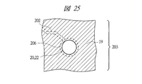
- FIG. 25 shows a conventional wiring structure 203 with a signal wiring 202
- FIG. 26 shows a conventional wiring structure 205 connected to a power supply wiring or a ground wiring 204. This is an example.
- FIG. 24 and FIG. 10 are compared.
- the diameter of the opening 20 to which the solder bump is connected which is defined by opening the polyimide, is the same in both cases.
- the electrode area 206 is set larger than that of a normal rewiring layer formed under the surface layer 19 made of polyimide shown in FIG. By changing this shape, the temperature in the chip can be made more uniform.
- the wiring structure shown in FIG. 10 is also clearly different from the conventional wiring structure shown in FIGS. 25 and 26 having lead-out wiring, and an opening 20 to which solder bumps are connected, which is defined by opening polyimide.
- the diameters of all of these are the same, but there is no lead wiring, but the dummy wiring 17 is set to be larger than the electrode area 206 of the normal rewiring layer formed under the surface layer 19 of normal polyimide. It is a structure.
- solder bumps on which the signal wirings 13 are formed have electrodes with a slow temperature rise, it is also effective to add dummy lead-out wirings.
- the shape and width of this dummy wiring can be optimized by thermal simulation.
- the detailed structure such as the redistribution layer, solder bump, dummy wiring, etc. of the semiconductor chip described above, and physical properties such as specific heat, density, thermal conductivity of each material are input, and the bonding tool on the back surface of the semiconductor chip 10 is input.
- An optimum dummy wiring shape can be obtained by calculating the temperature of the solder bump portion after a certain period of time when heat is applied.
- thermocompression bonding In order to reduce the heat distribution between the electrodes on the semiconductor chip, dummy electrodes that are particularly problematic during thermocompression bonding are connected to the surrounding signal wiring, power wiring, and ground wiring. It is also possible to connect them. However, depending on the structure of the width and thickness of each layer of the semiconductor device and the rewiring layer, this method may affect the electrical characteristics of the semiconductor device through the polyimide layer and generate noise. For this reason, it is difficult to connect a dummy electrode, which is likely to be a problem at the time of thermocompression bonding, with surrounding electrodes, and using a dummy wiring is also effective in terms of electrical characteristics.
- ⁇ Flip chip BGA> A semiconductor device mounted with a semiconductor chip according to an embodiment of the present invention will be described with reference to FIG.
- the semiconductor shown in FIG. An example in which the chip 18 is actually applied will be shown.
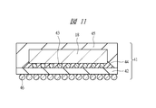
- the semiconductor device shown in FIG. 11 is a flip chip BGA (Ball Grid Array) 41, and a semiconductor chip 18 provided with dummy wirings is mounted on an interposer substrate (intermediate substrate).
- the thickness of the interposer substrate 42 is 0.8 mm, and the material is mainly a glass epoxy organic substrate.
- the semiconductor chip 18 was aligned with the interposer substrate 42, the solder bumps 43 were melted by thermocompression bonding, the electrodes were connected, and the resin 44 was sealed between the semiconductor chip 18 and the interposer substrate 42. Further, the upper part was sealed with a mold resin 45, and solder bumps 46 of external terminals were attached to the back surface of the interposer substrate 42.
- thermocompression bonding is performed in the air, but the wettability is improved even if an inert gas such as N 2 is blown around the periphery. Further, it is effective to improve wettability by thinning the surface oxide film by performing Ar sputtering, plasma cleaning or the like on the solder surface before thermocompression bonding. In addition, it is also possible to supply flux to solder bumps or substrate electrodes and perform thermocompression bonding, and the use of flux improves wettability. In this case, cleaning may be performed, but if there is no problem in reliability thereafter, the resin may be sealed without cleaning.
- the mold resin 45 may be omitted.
- the semiconductor chip 18 When the semiconductor chip 18 generates a large amount of heat, it is possible to attach a heat radiation fin or the like to the upper surface of the semiconductor chip 18.
- a memory or the like may be stacked on the upper surface of the semiconductor chip 18 and connected by wire bonding using Au wires to form a so-called stacked package structure.
- an external terminal may be provided on the outer periphery of the interposer substrate 42 shown in FIG. 11 and connected to another package on which a memory or the like is mounted to form a PoP (Package on Package) structure.
- PoP Package on Package
- ⁇ CoC structure package> Another semiconductor device mounted with a semiconductor chip according to an embodiment of the present invention will be described with reference to FIG.
- a semiconductor chip provided with dummy wirings has a CoC (Chip on Chip) structure.
- CoC Chip on Chip
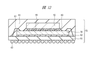
- the semiconductor device shown in FIG. 12 is a package 51 having a CoC structure, but this semiconductor chip 52 is drawn from the electrode 53 in order to improve the thermal uniformity in the chip during thermocompression bonding as shown in FIG.
- a dummy wiring 55 is provided in addition to the signal wiring 54.
- a polyimide layer 56 is formed thereon.
- a gap 57 is formed between the electrode 53 and the polyimide layer 56.
- This part consists of another polyimide layer below the electrode 53 layer. Even when the signal wiring 54 is formed in this way, it is effective to use the dummy wiring if the temperature does not rise uniformly during thermocompression bonding.
- the semiconductor chip 52 having this electrode structure was vacuum-adsorbed to the bonding head, and this was aligned with the electrode of another semiconductor chip 58, and thermocompression bonding was performed.
- the solder bump 59 was uniformly melted in a short time and connected to the electrode of another semiconductor chip 58.
- the resin 60 was sealed between the two chips, connected to the interposer substrate 61 by the die bond material 62, and the semiconductor chip 58 and the interposer substrate 61 were connected by the Au wire 63.
- the periphery was sealed with resin 64, and solder bumps 65 for external terminals were formed.
- the solder bump 59 may be formed only on the upper semiconductor chip 52 or the lower semiconductor chip 58, or may be formed on both semiconductor chips in order to increase the connection height. Further, dummy wiring can be provided on the semiconductor chip 58 or both, and the temperature distribution during thermocompression bonding can be reduced.
- the cost can be reduced by shortening the connection time, and the reliability can be improved by uniformizing the connection portion structure and interface state. It is possible.
- FIG. 14 shows a structure of a connection portion in a thermocompression bonding process in which a semiconductor chip is thermocompression bonded to an interposer substrate in the semiconductor device as described above.
- a thin semiconductor chip 71 having a thickness of 100 ⁇ m was vacuum-adsorbed to the bonding head 72 to eliminate chip warpage, and then aligned with the electrode 74 of the interposer substrate 73.
- the electrode 74 of the interposer substrate 73 has Ni plating (2 ⁇ m) on the Cu wiring and Au plating (0.1 ⁇ m) on the surface.
- the composition of the solder bump 75 on the semiconductor chip 71 is Sn-0.5Ag-0.7Cu, and the amount of Ag is smaller than that of normal Sn-3Ag-0.5Cu, because the amount of Ag3Sn in the solder is reduced and the solder is reduced. This is to improve the ductility of the metal and relax the stress generated in the connecting portion to improve the reliability.
- the pitch of the solder bumps 75 is 150 ⁇ m, and the height of the solder bumps 75 is 70 ⁇ m.
- This solder bump 75 was formed by filling a ball mounting mask having an opening corresponding to the re-wired electrode 76 of the semiconductor chip 71 with the solder ball, transferring it, and heating it.
- the semiconductor chip 71 is heated and pressed in the direction of the arrow (heat and pressure direction 77) in the drawing to melt the solder bump 75 and connect to the electrode 74 at the opening of the solder resist layer 81 on the interposer substrate 73. I let you.
- the thermocompression bonding conditions were performed by setting the tool temperature to 280 ° C., applying a load of 20 g, and heating and pressing for 10 seconds.
- FIG. 15 shows the wiring shape of one electrode in the semiconductor chip.
- Dummy wirings 78 are formed in three directions on the electrode 74, and signal wirings 79 are formed in one direction.
- a polyimide layer 80 is formed on the dummy wiring 78 and the signal wiring 79 except for the opening 82 of the polyimide layer.
- the dummy wiring 78 is determined by measuring the actual heat distribution, but may be determined by simulation of the surface temperature. Moreover, it is also possible to determine by a simple method in which the area of the wiring occupying a certain area around the electrode is substantially the same.
- the configuration of the electrode (also referred to as substrate electrode) 102 of the substrate 101 is the Ni layer 104 on the Cu layer 103 of the surface conductor layer, the Pd layer 105 on this surface, and further the Pd layer An Au layer 106 is formed on the surface of 105.
- the periphery of the electrode 102 is surrounded by a solder resist 107 which is an insulating material.
- the thermocompression bonding conditions are as follows. The surface opposite to the solder bump surface of the semiconductor chip 10 of FIG. 2 is vacuum-adsorbed to the bonding tool, aligned with the electrode 102 of the corresponding substrate 101, the bonding tool is lowered, and the solder contacts. After about 20 ⁇ m, the bonding tool was heated at 350 ° C.
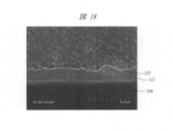
- FIG. 17 shows a cross section of the connecting portion 112 of the outermost solder bump (111 in FIG. 2) and the connecting portion 114 of the third solder bump (113 in FIG. 2) from the outermost periphery. From this, a flat interface compound layer 115 is formed at the interface between the outermost solder bump connection portion 112 and the substrate electrode 102, and the intermetallic compound 116 gathers in the solder structure near the electrode on the semiconductor chip 10 side.
- connection portion 114 of the third solder bump 113 from the outermost periphery the interface 118 with the substrate electrode 102 is formed by the compound 118 dispersed in the solder structure as the flat interface compound layer 115 shown in FIGS.
- one thin compound layer 119 was formed on the Ni layer 104.
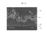
- the result of observing this connection interface with SEM is shown in FIG. From the observation result by SEM, a thin compound layer 119 was observed on the Ni layer 104, and the compound 118 dispersed in the solder structure 120 was observed.
- connection interface for each solder bump was examined in detail for other solder bump positions, and it was found that there was a correlation with the wiring structure in the substrate. That is, as can be seen from FIG. 17, the Cu wiring 126 is located immediately below the Cu layer 103 of the substrate electrode 102 for the outermost solder bump 111 via the interlayer insulating resin layer 108 made of glass epoxy resin. However, Cu wiring is also provided in the interlayer insulating resin layer 108 and in the inner layer of the substrate via the interlayer insulating resin layer 108 directly below the Cu layer 103 of the substrate electrode 102 for the third solder bump 113 from the outermost periphery. No. This is because each of the semiconductor chip electrodes plays a role, and therefore, the routing of the wiring inside the substrate is different for each electrode, thereby taking a different wiring structure around each substrate electrode.
- the heat transmitted through the semiconductor chip 10 and the connection part 112 in contact with the bonding tool is propagated to the surroundings by the Cu wiring 126. Therefore, it is considered that the time during which the solder bumps are actually melted is short.
- the heat transferred through the semiconductor chip 10 and the connection portion 114 in contact with the bonding tool does not exist in the connection portion because there is no Cu wiring layer directly under the electrode 102. It is estimated that the time during which the solder bumps are actually melted is longer than that of the outermost solder bump 111.
- a flat interface compound layer 115 is first formed at the connection interface with the substrate electrode 102.
- the outermost solder bump connection portion 112 has a short melting time.
- the temperature drops and solidifies, but the third solder bump connecting portion 114 from the outermost periphery is still melted at this stage, and the flat interfacial compound layer 115 generated at the beginning is peeled off, and the solder is formed in the solder. It is believed that it remained as dispersed compound 118.
- the difference in the intermetallic compound 116 deposited in the vicinity of the electrodes of the semiconductor chip 10 is considered to have a correlation with the magnitude of the temperature gradient inside the solder bump connection portion. That is, in the connection portion 112 of the outermost solder bump 111, heat escapes into the substrate, so the temperature of the substrate electrode is predicted to be low and the temperature gradient in the connection portion is large. A large amount of the intermetallic compound 116 was collected because it was in the vicinity of the interface with. However, in the connection part 114 of the third solder bump 113 from the outermost periphery, it is predicted that the compound is dispersed inside the solder and the temperature gradient in the connection part is small.
- the heating temperature of the substrate cannot be set high due to the heat resistance problem of the substrate, particularly in a short time thermocompression bonding process, and the difference between the bonding tool temperature and the substrate temperature becomes large, the wiring structure of the substrate Depending on the solder bump, the melted state is likely to be different for each solder bump, which appears to be a difference in the solder structure of the connecting portion and the connection interface structure.
- solder bumps were made of Sn-3Ag-0.5Cu.
- the connection structure is formed in the short-time thermocompression process by the wiring structure of the substrate. A difference has occurred.
- connection portion 112 of the outermost solder bump 111 where 115 remains when stress is generated at the end of the substrate electrode 102 and the end of the semiconductor chip 10 due to a temperature change during actual use, cracks occur near both interfaces. It is easy to break.
- connection portion 114 of the third solder bump 113 from the outermost periphery where the compound tends to be uniformly dispersed in the solder it is not easily broken when stress is concentrated on the electrode end portion, and the thermal fatigue reliability It is considered that the nature is high.
- thermocompression bonding process since the actual heating temperature in the thermocompression bonding process varies from solder bump to solder bump, the amount of electrode material dissolved into the solder bump differs, resulting in differences in solder physical properties such as mechanical characteristics and melting characteristics. .
- connection parts with different thermal fatigue characteristics, solder physical properties, etc.
- the substrate electrode is Cu / Ni / Pd / Au
- the surface layer is, for example, Cu / Ni / Au, Cu / Au, Cu alone, or an electrode obtained by subjecting Cu to rust prevention treatment.
- the thickness of the compound layer is different, the amount of electrode material that dissolves in the solder is different, and the physical properties of the solder (mechanical properties, melting characteristics, etc.) are different. Therefore, it can be said that reliability design is difficult.
- a conductor wiring layer and an interlayer insulating resin layer are laminated, and a plurality of electrodes are formed on one or both outer surfaces by the conductor wiring layer.
- a dummy through hole is provided as a heat conduction wiring in the substrate so that the heat distribution between the electrodes in the substrate is uniform. It has a structure in which holes and dummy wirings are formed.
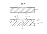
- FIG. 20 shows an example in which a dummy through hole 121 is formed immediately below the electrode 102 on the surface of the substrate 101. The through-hole depth and diameter of the dummy through-hole can be adjusted according to the heat distribution. This example is shown in FIG. 21, but a dummy through-hole 122 having a small diameter is formed.
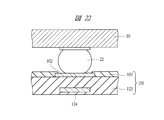
- FIG. 22 shows an example in which a dummy wiring is formed as a heat conduction wiring instead of a through hole.
- This substrate has a structure in which a dummy wiring 124 made of Cu is provided via an interlayer insulating resin layer 123 immediately below the electrode 102 on the surface of the substrate 101.
- the dummy wiring 124 corresponds to a different shape according to the heat distribution.
- the dummy wirings are difficult to distinguish from those of ordinary electrodes from the drawings showing one cross-sectional structure as shown in FIGS. Further, although not shown this time, it is difficult to understand the difference from the normal wiring structure from the diagram showing one planar structure. However, when considered three-dimensionally, the dummy wiring is characterized in that the leading end of the wiring is interrupted in the substrate, and unlike a normal wiring, the dummy wiring is electrically meaningless.
- the structure of both the semiconductor chip 10 and the substrate 101 is improved by providing wiring for heat conduction such as dummy wiring and dummy through-hole, thereby shortening the tact time of the thermocompression bonding process. And a highly reliable semiconductor device can be obtained.
- the effect obtained by a typical one is that when a thin semiconductor chip having solder bumps is connected by thermocompression bonding, the distribution of heat between each electrode on the semiconductor chip can be reduced, so that the connection margin is widened. Connection in a short time is possible, the number of production per unit time can be increased, and it can contribute to cost reduction.
- the heat distribution between the electrodes is almost uniform, the actual temperature load of the solder bumps is almost uniform, and the state of the interface compound, the structure, etc. are almost uniform between the electrodes, and the reliability design Can be facilitated and contribute to high reliability.
- the voids in the connection part which has been a problem in the past, can be improved in the void removability if the flowability of the solder can be sufficiently secured in any electrode, thereby contributing to the extension of the life of the connection part reliability.
- the semiconductor chip of the present invention and a semiconductor device mounted with the semiconductor chip can be used for semiconductor devices used in information equipment, portable equipment, automobile equipment, and the like.
- SYMBOLS 10 Semiconductor chip, 11 ... Al pad, 12 ... Electrode by solder bump, 13 ... Signal wiring, 14 ... Power supply wiring or ground wiring, 15 ... Electrode without lead-out wiring, 16 ... Solder bump spread in distorted, 17 ... dummy wiring, 18 ... semiconductor chip provided with dummy wiring, 19 ... surface layer made of polyimide, 20 ... opening to which solder bump is connected, 21 ... rewiring layer, 22 ... solder bump, 23 ... passivation film, 24 ... Polyimide layer, 25 ... redistribution layer, 26 ... Cr / Cu film, 27 ... Cu film, 28 ... Ni film, 41 ... flip chip BGA, 42 ...
- interposer substrate 43 ... solder bump, 44 ... resin, 45 ... mold resin 46 ... Solder bumps of external terminals, 51 ... CoC structure package, 52 ... Semiconductor chip provided with dummy wirings, 53 Electrode, 54 ... Signal wiring, 55 ... Dummy wiring, 56 ... Polyimide layer, 57 ... Gap between polyimide layer and electrode, 58 ... Separate semiconductor chip, 59 ... Solder bump, 60 ... Resin, 61 ... Interposer substrate, 62 ... Die bond material, 63 ... Au wire, 64 ... Resin, 65 ... Solder bump of external terminal, 71 ... Semiconductor chip, 72 ... Bonding head, 73 ... Interposer substrate, 74 ...
- the conventional wiring structure connected to the electrode 206, the electrode area of the normal rewiring layer formed under the surface layer of polyimide.
Landscapes
- Internal Circuitry In Semiconductor Integrated Circuit Devices (AREA)
Abstract
はんだバンプを有する薄型の半導体チップで、配線形状が電極毎に様々異なる場合でも、短時間に高歩留りで熱圧着し、高信頼な接続部を形成することを目的とした半導体装置を提供する。半導体チップ10において、半導体基板上の素子形成層に形成された回路に接続する複数の電極のうちの引き出し配線のない電極15には、電極に形成されるはんだバンプ22の溶融状態を均一にするためのダミー配線17が接続され、このダミー配線17は再配線層21によって形成されている。このように、半導体チップ10上のはんだバンプ22間の温度分布をなくすため、必要に応じて電極からダミー配線17を引き出し、半導体チップ10内の電極間の熱の均一性を図る。また、上記半導体チップに対応する基板にも、熱分布に応じてダミーの配線、スルーホールを形成し、電極間の熱分布を低減した構造とする。
Description
本発明は、半導体チップおよびこれを実装した半導体装置に関し、特に、半導体チップをはんだバンプにより基板、或いは別のチップに実装する構造の半導体装置に適用して有効な技術に関する。
本発明者が検討したところによれば、半導体装置に関しては、例えば、半導体チップの電極を基板電極、或いは別の半導体チップ電極に接続する場合、様々な方式がある。例えば、電極間をAu線によるワイヤボンディングにより接続する方式、チップ電極にAuバンプを形成し、このAuバンプを用いる方式、チップ電極にはんだバンプを形成し、これを用いて行う方式等がある。Auバンプは、チップ周辺のAlパッドによる電極に直接スタッドバンプにより形成できるために狭ピッチ化が可能であり、現在、80μmピッチ以下でもAuバンプを用いた接続が実用化されている。また、チップ周辺のAlパッドによる電極に、めっきによりAuバンプを形成することも可能である。
はんだバンプを使用する理由は主に2つあり、1つは、はんだバンプによる接続部は、Auバンプによる接続部に比べ、一般的に接続部の信頼性が高いためである。即ち、Auバンプによる接続部では、Auバンプ自体は柔らかく変形が可能であるが、例えばAuバンプを基板電極上に予め形成しておいたはんだ層を溶融させて接続した場合、硬くて脆いAuSnの化合物が接続部に析出するため、実使用時の熱の変化によって生じる応力、或いは材料間の熱膨張係数の違いによって生じる応力などが大きくなると、これらの応力を接続部で吸収することができず、亀裂が生じ、破断に至ってしまう。はんだ層を介さない方式として、AuバンプをAuめっき基板電極へ、超音波接続、熱圧着接続などで直接接続することも可能であるが、界面強度の確保、狭ピッチ化対応が難しい場合がある。
一方、はんだバンプを用いると、化合物は主に電極界面のみに生成され、接続部内部ははんだ成分で構成されることになる。はんだは様々な組成があるが、従来のSn-Pbはんだ、PbフリーはんだのSn系、Sn-Ag系、Sn-Cu系、Sn-Ag-Cu系はんだなどでは塑性変形が可能であり、使用時の熱によって生じた応力、材料間の熱膨張係数によって生じた応力などを、はんだ中の組織が変形することによって吸収することが可能である。このため、接続部の信頼性が高く、特に衝撃や振動が重要な問題となる自動車機器などに使用される半導体装置にも多く用いられている。
はんだバンプを用いる他の理由としては、電子機器の更なる高機能化により半導体チップの多ピン化が要求される場合、チップ周辺に配列されたAlパッドによる電極上のAuバンプを用いると、チップ外周で必要なピン数を確保しなくてはならないため、チップの面積が増大してしまう。携帯型電子機器の場合には、小型・薄型であることが重要で、内部に使用される半導体チップも小型・薄型であることが要求される。このため、高機能化により電極数が多ピン化してもチップ面積の増加は許されない。従って、電極間のピッチを狭くすることが必要であるが、狭ピッチ化にも製造上の限界がある。
そこで、チップ周辺のAlパッドによる電極からCuなどを用いてチップ上で再配線を行い、チップ面積全体に電極を引き出し、この電極上にはんだバンプを形成したWLP(Wafer Level Package)、或いはWPP(Wafer Process Package)等と言われる半導体チップ構造が用いられている(例えば特許文献1)。再配線された後の電極は、相手基板電極の引き回しの関係から、チップ面積全体に配列されていても良いし、チップ周囲に数列で配列されていても良い。再配線された各電極へのはんだバンプの形成は、レジストを利用しためっきによる方法、はんだボールを搭載し溶融させて形成する方法、はんだペーストの印刷により形成する方法など様々あり、それぞれの方式で、形成しやすいはんだバンプ高さ、組成に特徴がある。
また、特に携帯型電子機器の薄型化の要求により、チップの厚みが薄くなっている。現在、200μm厚み以下のチップが実用化されているが、研究開発では20μm厚程度までの薄型化が可能である。
一方、上記の半導体チップを搭載する基板は、更に装置本体のマザー基板に接続されることが多く、中間基板、インターポーザ基板等といわれるが、導体配線層と層間絶縁樹脂層が積層されるとともに、片方、または、両方の最表面に上記導体配線層によって複数の電極が形成され、これ以外が表面絶縁樹脂層により覆われているプリント配線板が用いられている。この基板は、例えば、絶縁樹脂材料からなるコア層の表面に通常Cuによる配線を形成し、この表面に層間絶縁樹脂層を形成し、スルーホールによって上下層の配線をつなぎ、更にこの層間絶縁樹脂層上に通常Cuによる導体配線層を形成する工程を繰り返し、必要な層数の配線層を形成したプリント配線板(いわゆるビルドアップ基板)が用いられている。現在、基板も薄型化が必要であり、コア層がない基板も提案されている。上記導体配線層は通常Cuであり、最表面に形成された電極は、Cu、或いは、Cu上に表面保護膜としての有機層、或いは、ぬれ性を向上させるためにCu上にNi層を形成し、その表面にAu層が形成されている構造、或いはCu上にAu層、或いは、Cu上にNi層を形成し、その表面にPd層、その表面にAu層を形成した構造になっている。また、前記表面絶縁樹脂層には通常、隣接はんだバンプ間のブリッジを防ぐため、及び電極以外の表面配線層の保護のためにソルダーレジストが用いられている。
ところで、前記のような半導体装置の技術において、はんだバンプによる半導体チップを接続する場合、半導体チップが厚い場合には、相手側の基板電極或いはチップ電極に位置合わせして搭載し、リフロー炉により加熱してはんだを溶融させ、基板電極、或いは、チップ電極に接続が可能である。
しかし、半導体チップが薄型化している場合、デバイスが形成されている面と形成されていない面で表面の応力が異なり、チップに反りが生じている。例えば、直径300mmのウェハでは、ウェハのデバイスの密度などによっても異なるが、ウェハの厚みが400μmのときの反りは約2mmであるが、200μm厚での反りは約10mm、100μm厚での反りは約50mm、50μm厚ではウェハは丸くなり、薄くなるにつれて反り量は大きくなる。従って、薄型の半導体チップの場合には位置合わせし、リフロー炉で加熱してはんだバンプを十分溶融させても、相手の基板電極、或いはチップ電極に接触せず、接続が不可能になる。このため、半導体チップに反りの矯正治具などを用いることが考えられるが、位置ずれなどの問題もあり、薄型の半導体チップをリフロー炉により加熱して接続することは難しいといえる。
そこで、薄型の半導体チップを平らなツールに真空吸着して反りを解消し、相手の基板電極、チップ電極との位置合わせを行い、熱圧着により接続する工法が考えられる。例えば、フリップチップボンダなどを使用し、平らなボンディングヘッドに薄型チップを真空吸着し、位置合わせし、ボンディングヘッドから熱を供給してはんだバンプを溶融させたものを、基板電極、或いはチップ電極に加圧して接触させ、はんだを接続させる。これにより、薄型の半導体チップでも反りの問題がなく接続が可能である。
しかし、ここで問題となるのが、溶融したはんだバンプを加圧する場合、溶融はんだは液体であるため、はんだバンプが容易に変形して大きくつぶれやすく、隣接バンプどうしが接触してはんだブリッジなどが生じたりする。従って、はんだバンプを熱圧着する場合には、ブリッジしないように低荷重で制御することが要求される。
また、リフロー炉による加熱・接続から熱圧着による加熱・接続に移行した場合に生じる問題として、単位時間当たりの生産数が減少する問題がある。即ち、リフロー炉による加熱では、一度に多くの試料(チップと基板の組み合わせ)を炉内に入れることが可能であるため、単位時間当たりの生産数を多く確保でき、且つ、加熱時間を十分とることができる。例えばSn-Ag共晶はんだ(Sn3.5Ag:融点221℃)によるはんだバンプを用いた場合、溶融温度の221℃以上を約30秒以上確保することが可能で、相手電極への接続に十分な時間を確保できる。更に、予熱も行うこともでき、チップ、基板等の熱伝導の違いによる熱分布を抑えることも可能である。
しかし、熱圧着による方法では、1つのボンディングヘッドを持つボンディング装置では、半導体チップ1個毎の接続となる。このため、1つの半導体チップと基板、或いはチップとの接続にかけられる時間が短くなり、単位時間当たりの生産数が少ないことが問題となってくる。即ち、上記のSn-Ag共晶はんだ(Sn3.5Ag:融点221℃)によるはんだバンプを用いた場合を例にとると、ボンディングヘッドへの半導体チップの吸着、位置合わせに必要な時間も考えると、溶融温度の221℃以上において、約10秒以下での接続、更に生産台数が多い場合には、221℃以上が約5秒以下での接続が必要な場合もある。
そこで、本発明は、これらの問題を解決して、はんだバンプを有する薄型の半導体チップで、配線形状が電極毎に様々異なる場合でも、短時間に高歩留りで熱圧着し、高信頼な接続部を形成することを目的とした半導体装置を提供するものである。
かつ、本発明は、これらの問題を解決して、複数の電極を有するプリント配線板で配線形状、周囲の配線構造が電極毎に様々異なる場合でも、短時間に高歩留りで熱圧着し、高信頼な接続部を形成することを目的とした半導体装置を提供するものである。
本発明の前記ならびにその他の目的と新規な特徴は、本明細書の記述および添付図面から明らかになるであろう。
本願において開示される発明のうち、代表的なものの概要を簡単に説明すれば、次のとおりである。
すなわち、代表的なものの概要は、半導体基板上の素子形成層に形成された回路に接続する複数の電極のうちの第1の電極には、複数の電極各々に1個ずつ形成される複数のはんだバンプの溶融状態の差を小さくするための(理想的にははんだバンプの溶融状態を均一にするための)熱伝導用配線が接続され、この熱伝導用配線は再配線によって形成されていることを特徴とする。具体的には、半導体チップのデバイス面上の周辺のAlパッドによる電極から再配線によりチップエリア全体または一部に電極を形成する時点で、各電極の引き出し配線を、電気的な配線という意味だけでなく、熱の供給パスとして考え、熱の供給量がある程度均一になるように、グランド配線、電源用配線、信号用配線の他に、熱伝導用配線としてのダミーの配線を設ける電極構造とする。このときのダミーの配線は、電気的な信号に影響を与えない方向で、一方向のみでも良いが、何方向かにダミーの配線を形成しても良い。また、引き出し配線のない電極のみではなく、グランド配線、電源用配線、信号用配線を有する電極でも、はんだの溶融状態を均一にするために、ダミーの配線を設けても良い。
同様に、上記半導体チップに対応する基板表面の複数の電極についても、接続時の電極の温度を均一にするための熱伝導用配線が形成されている構造とする。具体的には、熱分布の生じた電極の直下にダミーのスルーホールを形成した構造、前記ダミーのスルーホールの形状(径、深さ)は、電極の熱分布に応じて異なる構造、或いは、前記電極に接する表面絶縁樹脂層の直下に熱伝導用配線を形成する構造、この熱伝導用配線の形状は、電極の熱分布に応じて異なる構造である。また、表面層に1方向、或いは、何方向かにダミーの配線を設けても良い。
半導体装置の組み立てには、上記のように、均熱化を図った半導体チップ、或いは均熱化を図った基板のどちらか、或いは両方を用いる。
本発明によれば、はんだバンプを有する薄型の半導体チップであって、配線形状が電極毎に様々異なる場合でも、短時間に高歩留りで熱圧着し、高信頼な接続部を有する半導体装置を提供することができる。
また、同様に、配線形状が電極毎に様々異なる基板でも、短時間に高歩留りで熱圧着し、高信頼な接続部を有する半導体装置を提供することができる。
上記のような、均熱性を向上させた半導体チップ、或いは基板を用いることで高信頼な接続部を有する半導体装置を提供できるが、この両方を組み合わせて用いることにより、より短時間、高歩留りで接続できる。
以下、本発明の実施の形態を図面に基づいて詳細に説明する。なお、実施の形態を説明するための全図において、同一の部材には原則として同一の符号を付し、その繰り返しの説明は省略する。
<実施の形態の概要>
本発明の実施の形態の半導体装置は、チップ周辺のAlパッドによる電極からCuなどを用いてチップ上で再配線を行い、チップ面積全体に電極を引き出し、この電極上にはんだバンプを形成したWLP、或いはWPP等と言われる半導体チップ構造が用いられている。再配線された後の電極は、相手基板電極の引き回しの関係から、チップ面積全体に配列されていても良いし、チップ周囲に数列で配列されていても良い。
本発明の実施の形態の半導体装置は、チップ周辺のAlパッドによる電極からCuなどを用いてチップ上で再配線を行い、チップ面積全体に電極を引き出し、この電極上にはんだバンプを形成したWLP、或いはWPP等と言われる半導体チップ構造が用いられている。再配線された後の電極は、相手基板電極の引き回しの関係から、チップ面積全体に配列されていても良いし、チップ周囲に数列で配列されていても良い。
また、薄型の半導体チップを平らなツールに真空吸着して反りを解消し、相手の基板電極、チップ電極との位置合わせを行い、熱圧着により接続する工法が用いられる。例えば、フリップチップボンダなどを使用し、平らなボンディングヘッドに薄型チップを真空吸着し、位置合わせし、ボンディングヘッドから熱を供給してはんだバンプを溶融させたものを、基板電極、或いはチップ電極に加圧して接触させ、はんだを接続させる。これにより、薄型の半導体チップでも反りの問題がなく接続が可能である。
以上から、はんだバンプを有する薄型の半導体チップを、高信頼で短時間に熱圧着により接続することを目的に、様々な接続条件等の検討を行った。この検討のなかで、半導体チップ上の電極からの引き出し配線の形状の影響により、熱圧着時の溶融したはんだの変形状態が電極毎に大きく異なることがわかった。具体的には、はんだバンプを有する半導体チップを加熱加圧したときのはんだの変形状態を詳細に観察、評価した結果、通常のグランド配線、電源用配線、信号用配線などが引き出されている電極では、はんだバンプはほぼ球状に広がり、十分溶融していた。しかし、特に、グランド配線、電源用配線、信号用配線が引き出されていないダミーの電極上のはんだバンプで、はんだが球状に広がらず、突起のあるいびつな形状に変形された。
これは、熱圧着時の半導体チップ背面からの熱の供給により、半導体チップ上の配線形状によって熱の分布が異なるためで、グランド配線、電源用配線、信号用配線のある電極では、配線からの熱伝導により温度上昇が速く、はんだバンプが十分に加熱されて溶融し、はんだの流動性が確保されて球状に広がることが可能である。一方、引き出し配線のない電極では、温度上昇が遅く、はんだバンプが十分に加熱されないために溶融が不十分であり、はんだの流動性が低く、球状にはんだが広がることができず、表面酸化膜の影響でいびつな形状になったものと考えられる。また、はんだの流動性の低下によってはんだバンプ内のボイドの抜け性も低下する。更に詳しく熱圧着後のはんだの形状変化を調査すると、グランド配線、電源用配線と、信号用配線間でも配線の太さが異なる場合、熱圧着後のはんだの形状が異なることがわかった。これらのはんだの形状の違いは、熱圧着時の熱を十分与えられなかった場合により顕著になる。
そこで、本発明の実施の形態では、はんだバンプを有する薄型の半導体チップで、配線形状が電極毎に様々異なる場合でも、短時間に高歩留りで熱圧着し、高信頼な接続部を形成することを目的とした半導体装置を提供するものであり、以下において具体例を詳細に説明する。
<半導体チップの再配線>
本発明の一実施の形態における半導体チップについて、図1~図10を用いて説明する。ここでは、本発明の特徴を分かりやすくするために、従来の技術と比較しながら説明する。本実施の形態では、250μmピッチで432個のはんだバンプが形成されている半導体チップに本発明を適用した例を示す。
本発明の一実施の形態における半導体チップについて、図1~図10を用いて説明する。ここでは、本発明の特徴を分かりやすくするために、従来の技術と比較しながら説明する。本実施の形態では、250μmピッチで432個のはんだバンプが形成されている半導体チップに本発明を適用した例を示す。
まず、図2は、本実施の形態(従来技術も同様)の半導体チップ全体を示す。半導体チップ10は、周辺にAlパッド11が配置され、再配線によって半導体チップ10上にエリアアレー状にはんだバンプによる電極12が形成されている。従って、Alパッド11より、はんだバンプによる電極12の方がピッチが広くなっていて、接続する基板の配線を引き回ししやすくなっている。この半導体チップ10は、半導体基板上の素子形成層に回路が形成され、素子形成層の表面に再配線によってはんだバンプによる電極12が形成されている。
図3は、従来技術の半導体チップ10の再配線の一部を示す。この半導体チップ10は、再配線により、はんだバンプによる電極12がチップデバイス面に配列されていて、各電極から信号用配線13や、電源用配線或いはグランド配線14が引き出されている。しかし、半導体チップ周辺のAlパッド11による電極数と、中央に再配線により配列されたはんだバンプによる電極12の電極数の関係から、全く引き出し配線のない電極15も存在する。これは、はんだバンプの配列は対称形の方がその後のアンダーフィル材の注入性、接続部の熱疲労信頼性が高いためで、電極数をそろえるためにはんだバンプを間引きした非対称の配列構造をとりたくないためである。
この半導体チップ10上のはんだバンプについて加熱加圧を行った結果を図4に示す。加熱加圧の条件は、チップデバイス面の背面を260℃のヒータに接触させ、はんだバンプが約40μmつぶれるように、半導体チップ10全体に約150gの負荷をかけた。雰囲気は大気中である。この結果、図4に示すように、信号用配線13につながる電極のはんだバンプと、電源用配線或いはグランド配線14につながるはんだバンプは丸く、周囲にほぼ均一に広がっているが、全く引き出し配線のない電極15ではんだバンプの周囲に突起ができ、いびつな形状に広がった。
図4に示したはんだバンプのうち、いびつに広がったはんだバンプ16をSEMにより観察した結果を図5に示す。図5に示すように、いびつに広がったはんだバンプ16は、はんだが球状でなく、周囲がとがった形状をしている。また図4からわかるように、はんだ表面の色もいびつな形状なはんだは茶色で、表面酸化膜が多く残っていると考えられる。
これは、図3に示したように、各はんだバンプの電極への引き出し配線の形状の違いにより、熱の伝導性が異なるためと考えられる。即ち、ボンディングヘッドによりチップのデバイス面の背面から加熱された場合、はんだバンプ毎に温度の上昇速度が異なり、電源用配線或いはグランド配線14につながるはんだバンプでは配線から熱が供給されてはんだの融点以上に十分達しているため、溶融したはんだは流動性が高く、ボイドの抜け性も良く、周囲に丸くほぼ均一に広がることができ、接続信頼性が高い。しかし、全く引き出し配線のない電極15上のはんだバンプは、はんだの融点以上の時間が十分確保できなかったため、はんだの流動性が低く、周囲にいびつに広がったものと考えられる。いびつな形状に広がると、隣接バンプとブリッジする確率が上昇し、且つ、表面の酸化膜が残っているためにぬれ性が低く、ボイドの抜け性も不十分で、接続部の信頼性が低いと予測される。
はんだの流動性の違いによるボイドの抜け性に関しては、図4からわかるように、電源用配線或いはグランド配線14に接続された電極では、はんだ中に大きな穴があいていて(図4の濃淡の白に近い部分)、ボイドが抜けた跡と見られるが、信号用配線13につながった電極には、小さな穴は見られたが、電源用配線或いはグランド配線14に接続された電極に見られたほどの穴は見られなかった。全く引き出し配線のない電極15では、穴はあまり明確に見られず、さらに、ボイドの抜け性が低いと考えられる。従って、電極からの配線形状によって、はんだの流動性に差が生じていることが考えられる。
そこで、本実施の形態では、図6(半導体チップの再配線の一部を示す)のような半導体チップとする。本実施の形態では、全く引き出し配線のない電極15にダミー配線(熱伝導用配線)17を設けて、ダミー配線を設けた半導体チップ18の構造とする。このようにダミー配線17を設けることにより、このダミー配線を設けた半導体チップ18のデバイス面の温度分布を低減することが可能である。
このダミー配線17を形成した電極構造の詳細を図1に示す。図1に示すように、半導体チップ10周辺のAl電極への引き出し配線のない電極15では、ダミー配線17が形成され、電極周囲の表面にポリイミドによる表面層19が形成されている。このポリイミドによる表面層19によって、はんだバンプが接続される開口部20が規定されていて、実際の再配線層21は円形の点線部分まである。開口部20にははんだバンプ22が形成されている。
続いて、本実施の形態の電極の断面形状と製造方法を説明する。ここでも、本実施の形態と従来技術とを比較しながら説明する。
まず始めに、図7は、従来技術のWPPの断面構造を示す。この構造は、始めに半導体チップ10の周辺にAlパッド11、表面にパッシベーション膜23が形成されている。このパッシベーション膜23の表面に、Alパッド11部分を開口したポリイミド層24が形成されている。このポリイミド層24は、感光性ポリイミド樹脂膜を全面に塗布し、熱処理(プリベーク)、露光、現像によりAlパッド11部分を開口した後、熱処理を施し、ポリイミド樹脂膜を硬化させることによって形成する。このポリイミド層24の表面に、再配線層25として、Cr/Cu膜26、Cu膜27、Ni膜28が積層構造で形成されている。この再配線層25は、スパッタにて電解めっきのシード層となるCr/Cuを全面成膜し、シード層上にフォトリソグラフィ技術によって再配線用の溝を設けたレジスト層を形成し、溝の内部にのみCu膜27、次いでNi膜28を形成し、レジスト層、及び、不要な部分のシード層(Cr/Cu)を除去することによって形成する。
半導体チップ10の表面には、はんだバンプ形成箇所を開口したポリイミドによる表面層19が形成されている。このポリイミドによる表面層19は、ポリイミド層24と同様の方法で形成する。次に、ポリイミドによる表面層19の開口部にはんだバンプ22が形成されている。このはんだバンプ22は、ポリイミドによる表面層19の開口部のNi面上に無電解Auめっきを行い、Auめっき膜を形成し、開口部に印刷方式、はんだボール搭載方式などではんだバンプ22を形成する。上記の無電解Auめっき層は薄いため、はんだバンプ接続時にはんだ中に溶解し、界面には層として残らないため、図7中には示していない。以上が、従来技術のWPPの再配線層の形成方法である。
これに対して、図8には、本実施の形態のダミー配線を有するWPPの断面構造を示す。本実施の形態では、引き出し配線のない電極15にダミー配線17を形成する。このダミー配線17を有する再配線層25の形成方法も、図7の場合と同じである。従って、本実施の形態のWPPにおいては、従来技術のWPPと同じ再配線の形成プロセスでダミー配線17が形成でき、製造コストの上昇にほとんどつながらないにもかかわらず、熱圧着時の歩留り向上に寄与することが可能である。
ダミー配線17の形状としては、半導体チップの性能に影響を与えないような方向に引き出すことが重要である。従って、前述した図1の例では、一方向にダミー配線17を引き出したが、図9(ダミー配線を形成した電極構造の別の例)に示すように、複数の方向(図9では4方向の例)にダミー配線17を引き出しても良い。従って、前述した図6に示したようにダミー配線17を用いた場合には、どのはんだバンプでも、加熱加圧時に温度上昇が均一で、温度上昇の低いはんだバンプがいびつに広がることがなく、隣接バンプとのブリッジが起きにくくなり、接続時のマージンを確保することができる。また、他の電極構造の別の例を図10に示すが、ダミー配線17として、隣接バンプとの幅にもよるが、ポリイミドによる表面層19の下の再配線層21をポリイミド層の開口部20よりも極端に大きくとることも可能である。
この図10に示した実施の形態について、図24、図25、図26に示した従来の配線構造と比較して説明する。図24は引き出し配線のない場合の従来の配線構造201、図25は信号用配線202のある従来の配線構造203、図26は電源用配線、或いはグランド配線204とつながっている従来の配線構造205の例を示したものである。
まず、図24と図10を比較するが、ポリイミドを開口して規定した、はんだバンプが接続される開口部20の径の大きさは両者で同じであるが、ダミー配線17の部分が、図24に示したポリイミドによる表面層19の下に形成された通常の再配線層による電極面積206より大きく設定されている。この形状をかえることにより、チップ内温度をより均一に近づけることが可能である。
引き出し配線のある図25、図26に示した従来の配線構造とも、図10に示した配線構造は明らかに異なるものであり、ポリイミドを開口して規定した、はんだバンプが接続される開口部20の径の大きさは全て同じであるが、引き出し配線はないが、ダミー配線17の部分が通常のポリイミドによる表面層19の下に形成された通常の再配線層による電極面積206より大きく設定されている構造である。
また、信号用配線13が形成されているはんだバンプでも、温度上昇が遅い電極があれば、ダミーの引き出し配線を追加することも効果がある。
このダミー配線の形状、幅などは、熱のシミュレーションによって最適化することが可能である。例えば、上記の半導体チップの再配線層やはんだバンプ、ダミー配線等の詳細な構造、それぞれの材料の比熱、密度、熱伝導率などの物性値を入力し、半導体チップ10の背面のボンディングツールから熱が投入された時の、ある時間経過後のはんだバンプ部分の温度を計算によって求めることにより、最適なダミー配線形状を求めることができる。
なお、半導体チップ上の各電極間での熱の分布を低減するために、熱圧着時に特に問題になりやすいダミーの電極を周囲の信号用配線、電源用配線、グランド配線に接続されている電極とつなげてしまうことも考えられる。しかし、半導体デバイス、再配線層の各層の幅、厚みなどの構造にもよるが、この方法では、ポリイミド層を介して半導体デバイスの電気的な特性に影響を与え、ノイズを発生させる可能性があるため、熱圧着時に問題となりやすいダミーの電極を、周囲の電極とつなげることは難しく、ダミーの配線を用いることは、電気的特性の面からも効果がある。
<フリップチップBGA>
本発明の一実施の形態における半導体チップを実装した半導体装置について、図11を用いて説明する。本実施の形態では、半導体チップと、この半導体チップを実装した中間基板とを有する半導体装置の一例として、前記図6に示した、ダミー配線により熱圧着時の温度の均一性を向上させた半導体チップ18を実際に適用した例を示す。
本発明の一実施の形態における半導体チップを実装した半導体装置について、図11を用いて説明する。本実施の形態では、半導体チップと、この半導体チップを実装した中間基板とを有する半導体装置の一例として、前記図6に示した、ダミー配線により熱圧着時の温度の均一性を向上させた半導体チップ18を実際に適用した例を示す。
図11に示す半導体装置は、フリップチップBGA(Ball Grid Array)41であり、ダミー配線を設けた半導体チップ18がインターポーザ基板(中間基板)42に実装されている。インターポーザ基板42の厚みは0.8mmであり、材質は主にガラスエポキシ系の有機基板である。製造方法は、まず半導体チップ18をインターポーザ基板42に位置合わせし、熱圧着によりはんだバンプ43を溶融させて、電極間を接続し、半導体チップ18とインターポーザ基板42の間に樹脂44を封入した。更に上部をモールド樹脂45により封止し、インターポーザ基板42の裏面に外部端子のはんだバンプ46を取り付けることにより製作した。
この製造方法では、熱圧着は大気中で行ったが、N2等の不活性ガスを周囲に吹き付けてもぬれ性が向上する。また、熱圧着前にはんだ表面をArスパッタ、プラズマ洗浄等を行い、表面酸化膜を薄くしておくこともぬれ性向上に効果がある。他にも、フラックスをはんだバンプ、或いは基板電極に供給し、熱圧着を行うことも可能で、フラックスの使用によりぬれ性が向上する。この場合、洗浄はしても良いが、その後の信頼性に問題がなければ、洗浄せずに樹脂を封入しても良い。
なお、フリップチップBGA41では、モールド樹脂45はなくても良い。半導体チップ18の発熱が大きい場合には、放熱用のフィン等を半導体チップ18の上面に取り付けることも可能である。また、メモリなどを上記の半導体チップ18の上面に積層し、Au線によるワイヤボンディングにより接続し、いわゆる積層パッケージの構造としても良い。また、図11に示したインターポーザ基板42の外周に外部端子を設け、メモリ等を搭載した別パッケージと接続してPoP(Package on Package)の構造としても良い。
<CoC構造のパッケージ>
本発明の一実施の形態における半導体チップを実装した別の半導体装置について、図12を用いて説明する。本実施の形態では、積層した複数の半導体チップと、この積層した複数の半導体チップを実装した中間基板とを有する半導体装置の一例として、ダミー配線を設けた半導体チップをCoC(Chip on Chip)構造のパッケージに応用した例を示す。
本発明の一実施の形態における半導体チップを実装した別の半導体装置について、図12を用いて説明する。本実施の形態では、積層した複数の半導体チップと、この積層した複数の半導体チップを実装した中間基板とを有する半導体装置の一例として、ダミー配線を設けた半導体チップをCoC(Chip on Chip)構造のパッケージに応用した例を示す。
図12に示す半導体装置は、CoC構造のパッケージ51であるが、この半導体チップ52には図13に示したように熱圧着時のチップ内の均熱性を向上させるために、電極53から引き出されている信号用配線54の他にダミー配線55が設けてある。それぞれの引き出された信号用配線54、ダミー配線55を保護するために、この上にポリイミド層56が形成されているが、この場合、電極53の周囲にはポリイミド層56との間に隙間57があり、この部分は電極53の層の下にある別のポリイミド層からなっている。このように信号用配線54が形成されている場合でも、熱圧着時に均一に温度上昇しない場合には、ダミー配線を用いることが効果がある。
この電極構造を持つ半導体チップ52をボンディングヘッドに真空吸着し、これを別の半導体チップ58の電極に位置合わせし、熱圧着を行った。この結果、図12に示したように、はんだバンプ59は短時間に均一に溶融し、別の半導体チップ58の電極に接続された。この後、両チップ間に樹脂60を封入し、インターポーザ基板61にダイボンド材62により接続して、半導体チップ58とインタポーザ基板61をAu線63により接続した。次に、周囲を樹脂64で封止し、且つ外部端子のはんだバンプ65を形成した。
なお、はんだバンプ59は、上面の半導体チップ52、或いは下面の半導体チップ58にのみ形成しても良く、また接続高さを増すために、両方の半導体チップ上に形成しても良い。また、ダミー配線を半導体チップ58、或いは両方に設けることも可能で、熱圧着時の温度分布を低減することが可能である。
このように、CoC構造のパッケージ51においても、はんだバンプによる接続部に本発明を適用することで、接続時間の短縮による低コスト化、接続部組織、界面状態の均一化による信頼性向上を図ることが可能である。
<熱圧着工程>
前述したような半導体装置において、半導体チップをインターポーザ基板に熱圧着する熱圧着工程における接続部の構造を図14に示す。
前述したような半導体装置において、半導体チップをインターポーザ基板に熱圧着する熱圧着工程における接続部の構造を図14に示す。
100μm厚の薄型の半導体チップ71をボンディングヘッド72に真空吸着し、チップ反りを解消した後、インターポーザ基板73の電極74に位置合わせした。インターポーザ基板73の電極74はCu配線上にNiめっき(2μm)、この表面にAuめっき(0.1μm)を施している。半導体チップ71上のはんだバンプ75の組成はSn-0.5Ag-0.7Cuであり、通常のSn-3Ag-0.5CuよりAg量が少ないのは、はんだ中のAg3Sn量を低減させてはんだの延性を向上させ、接続部に生じる応力を緩和させて信頼性を向上させるためである。はんだバンプ75のピッチは150μmであり、はんだバンプ75の高さは70μmである。
このはんだバンプ75は、半導体チップ71の再配線した電極76に合わせた開口を持つボール搭載用マスクに、はんだボールを充填し、これを転写し、加熱することにより形成した。この半導体チップ71を図中の矢印(加熱加圧の方向77)の方向に加熱加圧を行い、はんだバンプ75を溶融させてインターポーザ基板73上のソルダレジスト層81の開口部の電極74に接続させた。熱圧着条件は、ツール温度を280℃に設定し、20gの荷重を負荷し、10秒間加熱加圧して行った。
この半導体チップの中の1つの電極の配線形状を図15に示すが、電極74にダミー配線78が3方向に形成され、信号用配線79は1方向に形成されている。これらのダミー配線78、信号用配線79の上にポリイミド層80が、このポリイミド層の開口部82を除いて形成されている。
なお、このダミー配線78は、実際の熱の分布を測定して決定したが、表面温度のシミュレーションにより決めても良い。また、電極周囲のある一定面積に占める配線の面積をほぼ同じにするという簡易的な方法で決めることも可能である。
<プリント基板の均熱化>
また、従来のダミー配線のないはんだバンプで構成された半導体チップを、実際の基板電極に短時間の熱圧着による接続を行い、接続部組織を詳細に観察したところ、以下のことがわかった。具体的には、図2に示した半導体チップ10でダミー配線による熱伝導配線を形成していないはんだバンプによる電極12を、対応する基板電極に接続した。半導体チップ10のはんだバンプによる電極12のピッチは250μmであり、はんだ組成はSn-3Ag-0.5Cuを用いた。基板の電極構成を図16に示したが、基板101の電極(基板電極とも記す)102の構成は、表面導体層のCu層103上にNi層104、この表面にPd層105、更にPd層105の表面にAu層106が形成してある。この電極102の周囲は、絶縁材料であるソルダーレジスト107で囲まれている。熱圧着の条件は、ボンディングツールに図2の半導体チップ10のはんだバンプ面と反対の面を真空吸着し、対応する基板101の電極102へ位置合わせし、ボンディングツールを下降し、はんだが接触してから約20μm押し込んだ時点で、ボンディングツールの温度を350℃で10秒間、パルスヒートで加熱した。自然冷却後に半導体チップ10の真空吸着を解除し、ボンディングツールを引き上げた。このとき基板101はステージに真空吸着しているが、ステージの温度は80℃とした。雰囲気は大気中で行った。
また、従来のダミー配線のないはんだバンプで構成された半導体チップを、実際の基板電極に短時間の熱圧着による接続を行い、接続部組織を詳細に観察したところ、以下のことがわかった。具体的には、図2に示した半導体チップ10でダミー配線による熱伝導配線を形成していないはんだバンプによる電極12を、対応する基板電極に接続した。半導体チップ10のはんだバンプによる電極12のピッチは250μmであり、はんだ組成はSn-3Ag-0.5Cuを用いた。基板の電極構成を図16に示したが、基板101の電極(基板電極とも記す)102の構成は、表面導体層のCu層103上にNi層104、この表面にPd層105、更にPd層105の表面にAu層106が形成してある。この電極102の周囲は、絶縁材料であるソルダーレジスト107で囲まれている。熱圧着の条件は、ボンディングツールに図2の半導体チップ10のはんだバンプ面と反対の面を真空吸着し、対応する基板101の電極102へ位置合わせし、ボンディングツールを下降し、はんだが接触してから約20μm押し込んだ時点で、ボンディングツールの温度を350℃で10秒間、パルスヒートで加熱した。自然冷却後に半導体チップ10の真空吸着を解除し、ボンディングツールを引き上げた。このとき基板101はステージに真空吸着しているが、ステージの温度は80℃とした。雰囲気は大気中で行った。
このように作成した試料を断面観察用のエポキシ樹脂に埋め込み、図2に示した半導体チップ10の最外周のはんだバンプの列(A-B切断面)で切断、研磨し、接続部の観察を行った。この実験を10個の半導体チップについて行い、半導体チップの接続部の代表的な観察結果を図17に示した。図17は、最外周のはんだバンプ(図2の111)の接続部112と、最外周から3個目のはんだバンプ(図2の113)の接続部114の断面を示したものである。これから、最外周のはんだバンプ接続部112の基板電極102との界面は、平らな界面化合物層115が形成されていて、半導体チップ10側の電極近傍のはんだ組織内には金属間化合物116が集まって析出していた。この基板電極との接続界面をSEMで観察した結果を図18に示すが、基板電極102とはんだの界面にはNi層104上に平らな界面化合物層115が形成され、この平らな界面化合物層115とNi層104の間にも薄い化合物層117が見られた。EDXによる組成分析の結果から、形成されていた平らな界面化合物層115には、PdとSnとAgが検出された。また、半導体チップ10の電極近傍に集まっていた金属間化合物116はAgとSnの化合物(Ag3Sn)であった。
一方、最外周から3個目のはんだバンプ113の接続部114では、基板電極102との界面は、図17、18に示した平らな界面化合物層115が剥がれはんだ組織内に分散した化合物118が見られ、Ni層104上に一層の薄い化合物層119が形成されていた。この接続界面をSEMで観察した結果を図19に示す。SEMでの観察結果からも、Ni層104上に薄い化合物層119が見られ、はんだ組織120中に分散した化合物118が見られた。EDXによる組成分析の結果から、はんだ組織内に分散した化合物118にはPdとSnとAgが検出され、図18で見られた化合物層115の成分とほぼ同じであり、図18の平らな界面化合物層115が剥がれてはんだ組織内に分散したものと推測された。また、図17から、半導体チップ界面近傍への金属間化合物の析出はあまり見られず、接続部114中に分散していた。
以上のようなはんだバンプ毎の接続界面の違いを、他のはんだバンプ位置についても詳細に検討したところ、基板内の配線構造と相関があることがわかった。即ち、図17からわかるように、最外周のはんだバンプ111用の基板電極102のCu層103の真下には、ガラスエポキシ樹脂からなる層間絶縁樹脂層108を介してCu配線126が有る。しかし、最外周から3個目のはんだバンプ113用の基板電極102のCu層103の真下には、層間絶縁樹脂層108中、及び層間絶縁樹脂層108を介した基板の内層にもCu配線が無い。これは、半導体チップ電極のそれぞれ役割を果たすため、基板内部の配線の引き回しが各電極毎に異なり、これによって各基板電極周辺で個々に異なる配線構造をとるためである。
従って、最外周のはんだバンプ111を短時間での熱圧着により接続する場合には、ボンディングツールに接した半導体チップ10、接続部112を通して伝えられた熱は、Cu配線126によって周囲に伝搬してしまい、実際にはんだバンプが溶融している時間が短いと考えられる。しかし、最外周から3個目のはんだバンプ113では、ボンディングツールに接した半導体チップ10、接続部114を通して伝えられた熱は、電極102の真下にCu配線層が無いため、接続部内に熱が留まり易く、実際にはんだバンプが溶融している時間が最外周のはんだバンプ111より長いと予測される。このため、ボンディングツールからの熱の供給により、まず始めに基板電極102との接続界面に平らな界面化合物層115が形成され、この段階で最外周のはんだバンプの接続部112は溶融時間が短いため温度が低下し凝固してしまうが、最外周から3個目のはんだバンプの接続部114はまだこの段階で溶融していて、始めに生じた平らな界面化合物層115が剥がれ、はんだ中に分散した化合物118として残ったと考えられる。
また、半導体チップ10の電極近傍に析出している金属間化合物116の違いについては、はんだバンプ接続部内部の温度勾配の大きさと相関があると考えられる。即ち、最外周のはんだバンプ111の接続部112では、基板内に熱が逃げるため、基板電極の温度が低く接続部内の温度勾配が大きいと予測され、はんだ接続部内部の最終凝固部が半導体チップ10との界面近傍であるため金属間化合物116が多く集まった。しかし、最外周から3個目のはんだバンプ113の接続部114でははんだ内部に化合物が分散し、接続部内の温度勾配が小さいと予測される。
このように、特に短時間の熱圧着工程で、基板の耐熱性の問題から基板の加熱温度を高く設定できず、ボンディングツール温度と基板温度との差が大きくなる場合には、基板の配線構造によってはんだバンプ毎に溶融状態が異なりやすく、接続部のはんだ組織、接続界面構造の違いとなって現れると考えられる。
上記の例では、はんだバンプはSn-3Ag-0.5Cuで行ったが、Ag量を0%~4%まで変えても、短時間の熱圧着工程では、基板の配線構造により接続部組織に違いが生じた。
はんだバンプ毎に接続部のはんだ組織、接続界面構造が異なることによる問題点としては、それぞれの接続部で熱疲労信頼性が異なることである。例えば図17に示した接続部の観察結果から、半導体チップ10との接続界面付近に硬い金属間化合物116が多く析出し、基板電極102の界面に本来剥がれるべき密着性の弱い平らな界面化合物層115が残っている最外周のはんだバンプ111の接続部112では、実使用時の温度変化により基板電極102端部、半導体チップ10電極端部に応力が生じたとき、両方の界面付近にクラックが入ったりして、壊れ易い。しかし、はんだ内部に化合物が均一に分散している傾向のある最外周から3個目のはんだバンプ113の接続部114では、同様に電極端部に応力が集中したときに壊れにくく、熱疲労信頼性が高いと考えられる。
他にも、熱圧着工程での実際の加熱温度がはんだバンプ毎に異なることにより、はんだバンプ内部への電極材料の溶け込み量が異なり、機械的特性、溶融特性等のはんだ物性にも違いが生じる。
このように熱疲労特性、はんだ物性等が異なる複数の接続部を有する場合には、信頼性設計が難しく、全てのはんだバンプで実使用時の温度変化に耐えうる接続部を確保することが困難である。ここでは、基板電極がCu/Ni/Pd/Auの場合を説明したが、表面層が例えば、Cu/Ni/Au、Cu/Au、Cuのみ、或いはCuに防錆処理を施した電極等の場合も同様であり、化合物層の厚みが異なったり、はんだ中に溶け込む電極材料の量に違いが生じ、はんだ物性(機械的性質、溶融特性など)が異なるなど、実際の温度条件の差に起因する違いが生じ、信頼性設計が難しいといえる。
そこで、以上説明したような課題を解決するために、本実施の形態では、導体配線層と層間絶縁樹脂層が積層されるとともに、片方、または、両方の最表面に導体配線層によって複数の電極が形成され、これ以外が表面絶縁樹脂層により覆われてなるプリント配線板による基板において、この基板内の電極間の熱分布が均一になるように、基板内に熱伝導用配線としてダミーのスルーホール、ダミーの配線を形成した構造をとる。具体的な構造例を示すが、図20に示したのは、基板101表面の電極102の直下にダミーのスルーホール121を形成した例である。ダミーのスルーホールは、熱分布に応じ、スルーホール深さ、径を調整することが可能であり、この例を図21に示したが、径の小さいダミーのスルーホール122が形成されている。
また、熱伝導用配線としてスルーホールではなく、ダミーの配線を形成した例を図22に示す。この基板では、基板101表面の電極102の直下に、層間絶縁樹脂層123を介してCuによるダミーの配線124を設けた構造である。このダミーの配線124は、熱分布に応じて形状を変えて対応する。
表面層の配置に余裕がある場合には、図23のように、表面の電極102に信号と問題のない方向にダミーの配線125を引き出すことも可能である。この場合も、熱分布に応じて形状を変えて対応する。
これらのダミー配線は、図20から図23に示したような1つの断面構造を示した図からは、通常の電極のものとの違いがわかりにくい。また、今回示していないが、1つの平面構造を示す図からも、通常の配線構造との違いがわかりにくい。しかし、ダミー配線は、3次元的に考えると、配線の先端が、基板内で途切れていることを特徴とし、通常の配線と異なり、電気的には意味のない配線である。
上記の図20から図23に示したような熱伝導用配線を有する基板を用いることにより、短時間の熱圧着での接続工程で、ボンディングツールから接続部を通して基板電極へ熱が供給されたとき、各バンプ間で基板内部に伝搬していく熱量の違いを低減することができる。このため、各はんだバンプ接続部の溶融温度条件がより均一になり、各接続部の界面構造、はんだ組織の違いが少なくなる。また、熱圧着条件設定が容易になり、且つ、接続部の構造がより均一になり、高信頼化を図ることが可能である。
更に高度に熱分布を低減するためには、半導体チップ10、基板101の両方の構造をダミー配線、ダミーのスルーホール等の熱伝導用配線を設けて改善することにより、熱圧着工程の短タクト化、高信頼化な半導体装置を得ることが可能となる。
以上、本発明者によってなされた発明を実施の形態に基づき具体的に説明したが、本発明は前記実施の形態に限定されるものではなく、その要旨を逸脱しない範囲で種々変更可能であることはいうまでもない。
本願において開示される発明のうち、代表的なものによって得られる効果を簡単に説明すれば以下のとおりである。
すなわち、代表的なものによって得られる効果は、はんだバンプを有する薄型の半導体チップを熱圧着で接続する場合、半導体チップ上の各電極間での熱の分布を低減できることから、接続マージンが広がり、短時間での接続が可能で、単位時間当たりの生産数を増すことができ、低コスト化に寄与できる。且つ、各電極間での熱の分布がほぼ均一なことから、はんだバンプの実際の温度負荷がほぼ均一になり、界面化合物の状態、組織等が各電極間でほぼ均一になり、信頼性設計が容易になり、高信頼化に寄与できる。さらに、従来問題になっている接続部中のボイドも、はんだの流動性がどの電極でも十分に確保できれば、ボイドの抜け性も向上し、接続部信頼性の長寿命化に寄与できる。また、従来は熱分布を均一にするために、ボンディングヘッドの温度を高めに設定する必要があったが、ヘッドの温度を必要最低限に抑えることが可能で、ボンディングヘッドの長寿命化にもつながり、低コスト化を図ることが可能である。
一方、基板の配線についても各電極間での熱の分布を低減できることから、均一な接続部を得ることが可能となり、熱圧着時間の短タクト化、接続部の高信頼化を図ることができる。
本発明の半導体チップおよびこれを実装した半導体装置は、情報機器、携帯用機器、自動車用機器などに使用される半導体装置に利用可能である。
10…半導体チップ、11…Alパッド、12…はんだバンプによる電極、13…信号用配線、14…電源用配線或いはグランド配線、15…引き出し配線のない電極、16…いびつに広がったはんだバンプ、17…ダミー配線、18…ダミー配線を設けた半導体チップ、19…ポリイミドによる表面層、20…はんだバンプが接続される開口部、21…再配線層、22…はんだバンプ、23…パッシベーション膜、24…ポリイミド層、25…再配線層、26…Cr/Cu膜、27…Cu膜、28…Ni膜、41…フリップチップBGA、42…インターポーザ基板、43…はんだバンプ、44…樹脂、45…モールド樹脂、46…外部端子のはんだバンプ、51…CoC構造のパッケージ、52…ダミー配線を設けた半導体チップ、53…電極、54…信号用配線、55…ダミー配線、56…ポリイミド層、57…ポリイミド層と電極の間の隙間、58…別の半導体チップ、59…はんだバンプ、60…樹脂、61…インターポーザ基板、62…ダイボンド材、63…Au線、64…樹脂、65…外部端子のはんだバンプ、71…半導体チップ、72…ボンディングヘッド、73…インターポーザ基板、74…電極、75…はんだバンプ、76…再配線した電極、77…加熱加圧の方向、78…ダミー配線、79…信号用配線、80…ポリイミド層、81…ソルダレジスト層、82…ポリイミド層の開口部、
101…基板、102…電極、103…Cu層、104…Ni層、105…Pd層、106…Au層、107…ソルダーレジスト、108…層間絶縁樹脂層、111…最外周のはんだバンプ、112…最外周のはんだバンプの接続部、113…最外周から3個目のはんだバンプ、114…最外周から3個目のはんだバンプの接続部、115…平らな界面化合物層、116…金属間化合物、117…薄い化合物層、118…分散した化合物、119…薄い化合物層、120…はんだ組織、121…ダミーのスルーホール、122…径の小さいダミーのスルーホール、123…層間絶縁樹脂層、124…基板内部のダミーの配線、125…基板表面のダミーの配線、126…Cu配線、
201…引き出し配線のない場合の従来の配線構造、202…信号用配線、203…信号用配線のある従来の配線構造、204…電源用配線、或いはグランド配線、205…電源用配線、或いはグランド配線とつながっている従来の配線構造、206…ポリイミドによる表面層の下に形成された通常の再配線層による電極面積。
101…基板、102…電極、103…Cu層、104…Ni層、105…Pd層、106…Au層、107…ソルダーレジスト、108…層間絶縁樹脂層、111…最外周のはんだバンプ、112…最外周のはんだバンプの接続部、113…最外周から3個目のはんだバンプ、114…最外周から3個目のはんだバンプの接続部、115…平らな界面化合物層、116…金属間化合物、117…薄い化合物層、118…分散した化合物、119…薄い化合物層、120…はんだ組織、121…ダミーのスルーホール、122…径の小さいダミーのスルーホール、123…層間絶縁樹脂層、124…基板内部のダミーの配線、125…基板表面のダミーの配線、126…Cu配線、
201…引き出し配線のない場合の従来の配線構造、202…信号用配線、203…信号用配線のある従来の配線構造、204…電源用配線、或いはグランド配線、205…電源用配線、或いはグランド配線とつながっている従来の配線構造、206…ポリイミドによる表面層の下に形成された通常の再配線層による電極面積。
Claims (24)
- 半導体基板上の素子形成層に形成された回路と、前記回路に接続され、前記素子形成層の表面に再配線によって形成された複数の電極と、前記複数の電極各々に形成された複数のはんだバンプと、を有する半導体チップであって、
前記複数の電極のうちの第1の電極には、熱伝導用配線が接続され、
前記熱伝導用配線は、前記再配線によって形成されていることを特徴とする半導体チップ。 - 請求項1記載の半導体チップにおいて、
前記熱伝導用配線は、前記複数のはんだバンプの溶融状態の差を小さくするための配線であることを特徴とする半導体チップ。 - 請求項1記載の半導体チップにおいて、
前記第1の電極は、信号用配線、電源用配線、およびグランド配線のいずれもが接続されない電極であることを特徴とする半導体チップ。 - 請求項1記載の半導体チップにおいて、
前記第1の電極は、信号用配線、電源用配線、およびグランド配線のいずれかが接続される電極であることを特徴とする半導体チップ。 - 半導体チップと、前記半導体チップを実装した中間基板とを有する半導体装置であって、
前記半導体チップは、
半導体基板上の素子形成層に形成された回路と、前記回路に接続され、前記素子形成層の表面に再配線によって形成された複数の電極と、前記複数の電極各々に形成された複数のはんだバンプと、を有し、
前記複数の電極のうちの第1の電極には、熱伝導用配線が接続され、
前記熱伝導用配線は、前記再配線によって形成されていることを特徴とする半導体装置。 - 請求項5記載の半導体装置において、
前記熱伝導用配線は、前記複数のはんだバンプの溶融状態の差を小さくするための配線であることを特徴とする半導体装置。 - 請求項5記載の半導体装置において、
前記第1の電極は、信号用配線、電源用配線、およびグランド配線のいずれもが接続されない電極であることを特徴とする半導体装置。 - 請求項5記載の半導体装置において、
前記第1の電極は、信号用配線、電源用配線、およびグランド配線のいずれかが接続される電極であることを特徴とする半導体装置。 - 請求項5記載の半導体装置において、
前記半導体チップは、熱圧着工程により前記中間基板に実装されていることを特徴とする半導体装置。 - 積層した複数の半導体チップと、前記積層した複数の半導体チップを実装した中間基板とを有する半導体装置であって、
前記積層した複数の半導体チップのうちの少なくとも1つの半導体チップは、
半導体基板上の素子形成層に形成された回路と、前記回路に接続され、前記素子形成層の表面に再配線によって形成された複数の電極と、前記複数の電極各々に形成された複数のはんだバンプと、を有し、
前記複数の電極のうちの第1の電極には、熱伝導用配線が接続され、
前記熱伝導用配線は、前記再配線によって形成されていることを特徴とする半導体装置。 - 請求項10記載の半導体装置において、
前記熱伝導用配線は、前記複数のはんだバンプの溶融状態の差を小さくするための配線であることを特徴とする半導体装置。 - 請求項10記載の半導体装置において、
前記第1の電極は、信号用配線、電源用配線、およびグランド配線のいずれもが接続されない電極であることを特徴とする半導体装置。 - 請求項10記載の半導体装置において、
前記第1の電極は、信号用配線、電源用配線、およびグランド配線のいずれかが接続される電極であることを特徴とする半導体装置。 - 請求項10記載の半導体装置において、
前記少なくとも1つの半導体チップは、熱圧着工程により前記中間基板に実装されていることを特徴とする半導体装置。 - 導体配線層と層間絶縁樹脂層が積層されるとともに、片方、または、両方の最表面に前記導体配線層によって複数の電極が形成され、これ以外が表面絶縁樹脂層により覆われてなるプリント配線板による中間基板であって、
前記複数の電極のうちの少なくとも1つの電極には、熱伝導用配線が形成されていることを特徴とする中間基板。 - 請求項15記載の中間基板において、
前記熱伝導用配線は、熱分布を小さくするための配線であることを特徴とする中間基板。 - 請求項15記載の中間基板において、
前記熱伝導用配線は、前記電極にダミーのスルーホールを接続した構造からなることを特徴とする中間基板。 - 請求項17記載の中間基板において、
前記熱伝導用配線は、前記電極にダミーのスルーホールを接続し、スルーホール径、スルーホール深さを変えて熱分布に対応した構造からなることを特徴とする中間基板。 - 請求項15記載の中間基板において、
前記熱伝導用配線は、前記電極に接する表面絶縁樹脂層の直下に形成されていることを特徴とする中間基板。 - 半導体チップと、前記半導体チップを実装した中間基板とを有する半導体装置であって、
前記半導体チップとして、請求項1に記載の半導体チップ、
前記中間基板として、請求項15に記載の中間基板、
の両方、またはどちらか片方を用いたことを特徴とする半導体装置。 - 半導体基板上の素子形成層に形成された回路と、前記素子形成層の表面に再配線によって形成された複数の電極と、前記複数の電極各々に形成された複数のはんだバンプと、を有する半導体チップであって、
前記複数の電極のうちの少なくとも1つの電極には、前記回路またはAlパッドと電気的に接続しない熱伝導用配線が形成されていることを特徴とする半導体チップ。 - 半導体チップと、前記半導体チップを実装した中間基板とを有する半導体装置であって、
前記半導体チップは、
半導体基板上の素子形成層に形成された回路と、前記素子形成層の表面に再配線によって形成された複数の電極と、前記複数の電極各々に形成された複数のはんだバンプと、を有し、
前記複数の電極のうちの少なくとも1つの電極には、前記回路またはAlパッドと電気的に接続しない熱伝導用配線が形成されていることを特徴とする半導体装置。 - 積層した複数の半導体チップと、前記積層した複数の半導体チップを実装した中間基板とを有する半導体装置であって、
前記積層した複数の半導体チップのうちの少なくとも1つの半導体チップは、
半導体基板上の素子形成層に形成された回路と、前記素子形成層の表面に再配線によって形成された複数の電極と、前記複数の電極各々に形成された複数のはんだバンプと、を有し、
前記複数の電極のうちの少なくとも1つの電極には、前記回路またはAlパッドと電気的に接続しない熱伝導用配線が形成されていることを特徴とする半導体装置。 - 導体配線層と層間絶縁樹脂層が積層されるとともに、片方、または、両方の最表面に前記導体配線層によって複数の電極が形成され、これ以外が表面絶縁樹脂層により覆われてなるプリント配線板による中間基板であって、
前記複数の電極のうちの少なくとも1つの電極には、回路またはAlパッドと電気的に接続しない熱伝導用配線が形成されていることを特徴とする中間基板。
Applications Claiming Priority (2)
| Application Number | Priority Date | Filing Date | Title |
|---|---|---|---|
| JP2008-137386 | 2008-05-27 | ||
| JP2008137386 | 2008-05-27 |
Publications (1)
| Publication Number | Publication Date |
|---|---|
| WO2009145196A1 true WO2009145196A1 (ja) | 2009-12-03 |
Family
ID=41377069
Family Applications (1)
| Application Number | Title | Priority Date | Filing Date |
|---|---|---|---|
| PCT/JP2009/059619 Ceased WO2009145196A1 (ja) | 2008-05-27 | 2009-05-26 | 半導体チップ、中間基板および半導体装置 |
Country Status (1)
| Country | Link |
|---|---|
| WO (1) | WO2009145196A1 (ja) |
Cited By (1)
| Publication number | Priority date | Publication date | Assignee | Title |
|---|---|---|---|---|
| JP2012043990A (ja) * | 2010-08-19 | 2012-03-01 | Fujikura Ltd | 配線基板 |
Citations (4)
| Publication number | Priority date | Publication date | Assignee | Title |
|---|---|---|---|---|
| JPH0883865A (ja) * | 1994-09-14 | 1996-03-26 | Citizen Watch Co Ltd | 樹脂封止型半導体装置 |
| JPH0964049A (ja) * | 1995-08-30 | 1997-03-07 | Oki Electric Ind Co Ltd | チップサイズパッケージ及びその製造方法 |
| JPH10214911A (ja) * | 1997-01-28 | 1998-08-11 | Toshiba Corp | 半導体装置搭載用基板 |
| JP2005294720A (ja) * | 2004-04-05 | 2005-10-20 | Seiko Epson Corp | 半導体装置及びその製造方法並びに電子機器 |
-
2009
- 2009-05-26 WO PCT/JP2009/059619 patent/WO2009145196A1/ja not_active Ceased
Patent Citations (4)
| Publication number | Priority date | Publication date | Assignee | Title |
|---|---|---|---|---|
| JPH0883865A (ja) * | 1994-09-14 | 1996-03-26 | Citizen Watch Co Ltd | 樹脂封止型半導体装置 |
| JPH0964049A (ja) * | 1995-08-30 | 1997-03-07 | Oki Electric Ind Co Ltd | チップサイズパッケージ及びその製造方法 |
| JPH10214911A (ja) * | 1997-01-28 | 1998-08-11 | Toshiba Corp | 半導体装置搭載用基板 |
| JP2005294720A (ja) * | 2004-04-05 | 2005-10-20 | Seiko Epson Corp | 半導体装置及びその製造方法並びに電子機器 |
Cited By (1)
| Publication number | Priority date | Publication date | Assignee | Title |
|---|---|---|---|---|
| JP2012043990A (ja) * | 2010-08-19 | 2012-03-01 | Fujikura Ltd | 配線基板 |
Similar Documents
| Publication | Publication Date | Title |
|---|---|---|
| JP3891838B2 (ja) | 半導体装置およびその製造方法 | |
| JP5649805B2 (ja) | 半導体装置の製造方法 | |
| US8710651B2 (en) | Semiconductor device and method for manufacturing the same | |
| US20020171152A1 (en) | Flip-chip-type semiconductor device and manufacturing method thereof | |
| JP4731495B2 (ja) | 半導体装置 | |
| JP4105409B2 (ja) | マルチチップモジュールの製造方法 | |
| US20060043603A1 (en) | Low temperature PB-free processing for semiconductor devices | |
| JP2008226946A (ja) | 半導体装置およびその製造方法 | |
| KR20090030192A (ko) | 패키지 기판 구조체 및 그 제조방법 | |
| CN102208388A (zh) | 半导体装置以及半导体装置的制造方法 | |
| TWI502666B (zh) | Electronic parts mounting body, electronic parts, substrate | |
| JP2009004454A (ja) | 電極構造体及びその形成方法と電子部品及び実装基板 | |
| KR20030090481A (ko) | 비도전성 접착제로 ic 칩을 기판에 본딩하는 방법과형성된 조립물 | |
| JP2011228704A (ja) | マクロピンハイブリッド相互接続アレイ及びその製造方法 | |
| JP2009200067A (ja) | 半導体チップおよび半導体装置 | |
| US20070120268A1 (en) | Intermediate connection for flip chip in packages | |
| US20100167466A1 (en) | Semiconductor package substrate with metal bumps | |
| US7755200B2 (en) | Methods and arrangements for forming solder joint connections | |
| US20090091036A1 (en) | Wafer structure with a buffer layer | |
| JP2002026073A (ja) | 半導体装置およびその製造方法 | |
| WO2009145196A1 (ja) | 半導体チップ、中間基板および半導体装置 | |
| TWI496250B (zh) | 封裝基板及其製法 | |
| TWI220304B (en) | Flip-chip package substrate and flip-chip bonding process thereof | |
| KR101009192B1 (ko) | 반도체 장치의 범프 구조물 및 그 제조방법 | |
| JP2002118210A (ja) | 半導体装置用インタポーザ及びこれを用いた半導体装置 |
Legal Events
| Date | Code | Title | Description |
|---|---|---|---|
| 121 | Ep: the epo has been informed by wipo that ep was designated in this application |
Ref document number: 09754704 Country of ref document: EP Kind code of ref document: A1 |
|
| NENP | Non-entry into the national phase |
Ref country code: DE |
|
| NENP | Non-entry into the national phase |
Ref country code: JP |
|
| 122 | Ep: pct application non-entry in european phase |
Ref document number: 09754704 Country of ref document: EP Kind code of ref document: A1 |