WO2009116552A1 - 非晶質炭素被覆工具 - Google Patents
非晶質炭素被覆工具 Download PDFInfo
- Publication number
- WO2009116552A1 WO2009116552A1 PCT/JP2009/055228 JP2009055228W WO2009116552A1 WO 2009116552 A1 WO2009116552 A1 WO 2009116552A1 JP 2009055228 W JP2009055228 W JP 2009055228W WO 2009116552 A1 WO2009116552 A1 WO 2009116552A1
- Authority
- WO
- WIPO (PCT)
- Prior art keywords
- amorphous carbon
- carbon film
- layer portion
- substrate
- coated tool
- Prior art date
- Legal status (The legal status is an assumption and is not a legal conclusion. Google has not performed a legal analysis and makes no representation as to the accuracy of the status listed.)
- Ceased
Links
Classifications
-
- C—CHEMISTRY; METALLURGY
- C23—COATING METALLIC MATERIAL; COATING MATERIAL WITH METALLIC MATERIAL; CHEMICAL SURFACE TREATMENT; DIFFUSION TREATMENT OF METALLIC MATERIAL; COATING BY VACUUM EVAPORATION, BY SPUTTERING, BY ION IMPLANTATION OR BY CHEMICAL VAPOUR DEPOSITION, IN GENERAL; INHIBITING CORROSION OF METALLIC MATERIAL OR INCRUSTATION IN GENERAL
- C23C—COATING METALLIC MATERIAL; COATING MATERIAL WITH METALLIC MATERIAL; SURFACE TREATMENT OF METALLIC MATERIAL BY DIFFUSION INTO THE SURFACE, BY CHEMICAL CONVERSION OR SUBSTITUTION; COATING BY VACUUM EVAPORATION, BY SPUTTERING, BY ION IMPLANTATION OR BY CHEMICAL VAPOUR DEPOSITION, IN GENERAL
- C23C14/00—Coating by vacuum evaporation, by sputtering or by ion implantation of the coating forming material
- C23C14/02—Pretreatment of the material to be coated
- C23C14/027—Graded interfaces
-
- C—CHEMISTRY; METALLURGY
- C23—COATING METALLIC MATERIAL; COATING MATERIAL WITH METALLIC MATERIAL; CHEMICAL SURFACE TREATMENT; DIFFUSION TREATMENT OF METALLIC MATERIAL; COATING BY VACUUM EVAPORATION, BY SPUTTERING, BY ION IMPLANTATION OR BY CHEMICAL VAPOUR DEPOSITION, IN GENERAL; INHIBITING CORROSION OF METALLIC MATERIAL OR INCRUSTATION IN GENERAL
- C23C—COATING METALLIC MATERIAL; COATING MATERIAL WITH METALLIC MATERIAL; SURFACE TREATMENT OF METALLIC MATERIAL BY DIFFUSION INTO THE SURFACE, BY CHEMICAL CONVERSION OR SUBSTITUTION; COATING BY VACUUM EVAPORATION, BY SPUTTERING, BY ION IMPLANTATION OR BY CHEMICAL VAPOUR DEPOSITION, IN GENERAL
- C23C14/00—Coating by vacuum evaporation, by sputtering or by ion implantation of the coating forming material
- C23C14/06—Coating by vacuum evaporation, by sputtering or by ion implantation of the coating forming material characterised by the coating material
- C23C14/0605—Carbon
-
- C—CHEMISTRY; METALLURGY
- C23—COATING METALLIC MATERIAL; COATING MATERIAL WITH METALLIC MATERIAL; CHEMICAL SURFACE TREATMENT; DIFFUSION TREATMENT OF METALLIC MATERIAL; COATING BY VACUUM EVAPORATION, BY SPUTTERING, BY ION IMPLANTATION OR BY CHEMICAL VAPOUR DEPOSITION, IN GENERAL; INHIBITING CORROSION OF METALLIC MATERIAL OR INCRUSTATION IN GENERAL
- C23C—COATING METALLIC MATERIAL; COATING MATERIAL WITH METALLIC MATERIAL; SURFACE TREATMENT OF METALLIC MATERIAL BY DIFFUSION INTO THE SURFACE, BY CHEMICAL CONVERSION OR SUBSTITUTION; COATING BY VACUUM EVAPORATION, BY SPUTTERING, BY ION IMPLANTATION OR BY CHEMICAL VAPOUR DEPOSITION, IN GENERAL
- C23C14/00—Coating by vacuum evaporation, by sputtering or by ion implantation of the coating forming material
- C23C14/22—Coating by vacuum evaporation, by sputtering or by ion implantation of the coating forming material characterised by the process of coating
- C23C14/24—Vacuum evaporation
- C23C14/32—Vacuum evaporation by explosion; by evaporation and subsequent ionisation of the vapours, e.g. ion-plating
- C23C14/325—Electric arc evaporation
-
- C—CHEMISTRY; METALLURGY
- C23—COATING METALLIC MATERIAL; COATING MATERIAL WITH METALLIC MATERIAL; CHEMICAL SURFACE TREATMENT; DIFFUSION TREATMENT OF METALLIC MATERIAL; COATING BY VACUUM EVAPORATION, BY SPUTTERING, BY ION IMPLANTATION OR BY CHEMICAL VAPOUR DEPOSITION, IN GENERAL; INHIBITING CORROSION OF METALLIC MATERIAL OR INCRUSTATION IN GENERAL
- C23C—COATING METALLIC MATERIAL; COATING MATERIAL WITH METALLIC MATERIAL; SURFACE TREATMENT OF METALLIC MATERIAL BY DIFFUSION INTO THE SURFACE, BY CHEMICAL CONVERSION OR SUBSTITUTION; COATING BY VACUUM EVAPORATION, BY SPUTTERING, BY ION IMPLANTATION OR BY CHEMICAL VAPOUR DEPOSITION, IN GENERAL
- C23C14/00—Coating by vacuum evaporation, by sputtering or by ion implantation of the coating forming material
- C23C14/22—Coating by vacuum evaporation, by sputtering or by ion implantation of the coating forming material characterised by the process of coating
- C23C14/34—Sputtering
- C23C14/3492—Variation of parameters during sputtering
-
- H—ELECTRICITY
- H05—ELECTRIC TECHNIQUES NOT OTHERWISE PROVIDED FOR
- H05K—PRINTED CIRCUITS; CASINGS OR CONSTRUCTIONAL DETAILS OF ELECTRIC APPARATUS; MANUFACTURE OF ASSEMBLAGES OF ELECTRICAL COMPONENTS
- H05K3/00—Apparatus or processes for manufacturing printed circuits
- H05K3/0011—Working of insulating substrates or insulating layers
- H05K3/0044—Mechanical working of the substrate, e.g. drilling or punching
- H05K3/0047—Drilling of holes
Definitions
- the present invention relates to an amorphous carbon-coated tool in which an amorphous carbon film is coated on a base material.
- amorphous carbon-coated tool As a conventional amorphous carbon-coated tool, there is an amorphous carbon-coated tool in which the amount of hydrogen in the amorphous carbon film is 5 atomic% or less (see, for example, Patent Document 1).
- a DLC having a two-layer structure of a base layer that substantially does not contain hydrogen and a hydrogen-containing layer that is provided on the base layer and contains hydrogen within a range of 2 atomic% to 20 atomic% There is a DLC film-coated tool coated with a diamond-like carbon film (for example, see Patent Document 2).
- these tools have a problem that the adhesion between the coating and the substrate is not sufficient.
- an object of the present invention is to provide an amorphous carbon-coated tool that is excellent in adhesion between an amorphous carbon film and a base material and is excellent in wear resistance.
- the present inventor has developed an amorphous carbon-coated tool.
- an amorphous carbon film having a large amount of hydrogen is coated on the side in contact with the substrate, and an amorphous carbon film having a small amount of hydrogen is coated on the upper surface thereof.
- the present invention was completed with the knowledge that an amorphous carbon-coated tool with excellent wear resistance and excellent adhesion between the amorphous carbon film and the substrate can be obtained. .
- the amorphous carbon-coated tool of the present invention includes a base material and an amorphous carbon film, and the amorphous carbon film is composed of an inner layer portion on the side in contact with the base material and an outer layer portion on the surface side.
- the amount of hydrogen contained in the inner layer portion of the crystalline carbon film is larger than the amount of hydrogen contained in the outer layer portion of the amorphous carbon film.
- Examples of the base material for the amorphous carbon-coated tool of the present invention include high-speed steel, cemented carbide, ceramics, and ultra-high pressure sintered body. Among these, cemented carbide is more preferable because it is excellent in hardness and toughness.
- the amorphous carbon film of the present invention includes what is called a hard carbon film, a diamond-like carbon film, a DLC film, an aC: H film, an i-carbon film, a ta-C film, and the like.
- the amorphous carbon film of the present invention is composed of an inner layer portion in contact with the substrate and an outer layer portion on the surface side.
- the amount of hydrogen contained in the inner layer portion of the amorphous carbon film is greater than the amount of hydrogen contained in the outer layer portion of the amorphous carbon film. This is because when the amount of hydrogen in the amorphous carbon film is low, the hardness of the amorphous carbon film is high, but the adhesion between the amorphous carbon film and the substrate is low. It is determined from the knowledge that, when the amount is high, the adhesion to the base material becomes high.
- the concentration of hydrogen in the inner layer portion of the amorphous carbon film has a concentration gradient that gradually decreases from the side in contact with the base material toward the surface side, it is possible to prevent adhesion and decrease in coating hardness. More preferable.
- the amount of hydrogen contained in the outer layer portion of the amorphous carbon film of the present invention is less than 0.5 atomic%, that is, an amount meaning that substantially no hydrogen is contained, and is contained in the inner layer portion of the amorphous carbon film. More preferably, the hydrogen content is 0.5-3 atomic%. This is because when the amount of hydrogen in the amorphous carbon film is less than 0.5 atomic%, the hardness of the amorphous carbon film is high, but the adhesion between the amorphous carbon film and the substrate is low, and the amorphous carbon film is amorphous.
- the amount of hydrogen in the amorphous carbon film and its concentration gradient are measured using elastic recoil detection method (ERDA) using high-energy ions such as helium as incident particles, resonance nuclear reaction method (NRA: Nuclear Reaction Analysis), etc. It can be measured by doing.
- the thickness of the inner layer portion in the amorphous carbon film of the present invention is preferably 1 to 10% of the entire thickness of the amorphous carbon film. If the thickness of the inner layer portion of the amorphous carbon film is less than 1% of the entire film thickness, the effect of increasing the wear resistance cannot be sufficiently obtained. The hardness of the entire film decreases. Therefore, the thickness of the outer layer portion of the amorphous carbon film is preferably 90 to 99% of the entire thickness of the amorphous carbon film.
- the amorphous carbon film of the present invention preferably has a hardness by nanoindentation of 20 to 100 GPa, more preferably 30 to 80 GPa. This is because if the hardness is less than 20 GPa, the wear resistance decreases, and if it exceeds 100 GPa, the chipping resistance of the cutting edge decreases.
- the elastic recovery rate of the amorphous carbon film of the present invention is easily plastically deformed when the elastic recovery rate is less than 70%, it preferably has an elastic recovery rate of 70 to 100%.
- the amorphous carbon film of the present invention preferably has a film thickness of 0.06 to 5 ⁇ m. If the film thickness is less than 0.06 ⁇ m, the effect of covering the amorphous carbon film cannot be obtained. If the film thickness exceeds 5 ⁇ m, the compressive stress of the amorphous carbon film increases, and Adhesion decreases.
- the compressive stress existing in the base material affects the chipping resistance and the adhesion between the amorphous carbon film and the base material. Regardless of the surface state of the substrate, the compressive stress present in the substrate is preferably 0.3 GPa or less. If the compressive stress of the substrate exceeds 0.3 GPa, chipping is likely to occur in the amorphous carbon film.
- the compressive stress existing in the base material can be measured by the 2 ⁇ -sin 2 ⁇ method, and specifically, the compressive stress of the base material can be measured using the following formulas 2 and 3.
- the compressive stress which exists in WC can be considered as the compressive stress which exists in a base material.
- Stress ⁇ -E / (2 ⁇ (1 + ⁇ )) ⁇ cot ⁇ 0 ⁇ ⁇ / 180 ⁇ ⁇ (2 ⁇ ) / ⁇ (sin 2 ⁇ )
- Stress ⁇ K ⁇ ⁇ (2 ⁇ ) / ⁇ (sin 2 ⁇ ) ⁇ : Angle between sample surface normal and lattice surface normal ⁇ : Stress (MPa) E: Young's modulus (MPa) ⁇ : Poisson's ratio ⁇ 0 : Standard Bragg angle (degrees) K: Constant determined by material properties and standard Bragg angle ⁇ 0
- the amorphous carbon film of the present invention has a first peak in the range of wave numbers 1560 to 1600 cm ⁇ 1 and a wave number of 1100 to 1200 cm in a Raman spectrum by Raman spectroscopy using an argon gas laser having a wavelength of 514.5 nm. More preferably, it has a second peak in the range of -1 .
- the Raman spectrum in the range of wave numbers 800 ⁇ 2000 cm -1 was measured, peaks hardly observed in the vicinity of a wave number of 1350 cm -1, if there is a first peak and second peak in the range of the wave number, amorphous It shows a tendency for the hardness of the carbon film to increase.
- the amorphous carbon film of the present invention has high hardness comparable to diamond, and exhibits excellent wear resistance when used as a cutting tool. Since the amorphous carbon film of the present invention has a high sp 3 bond ratio, the room temperature hardness and the high temperature hardness are increased.
- amorphous carbon-coated tool of the present invention include cutting tools such as drills, end mills, and throw-away tips, and dies.
- the amorphous carbon film of the present invention can be obtained by physical vapor deposition using solid carbon as a starting material.
- physical vapor deposition include arc ion plating, laser ablation, and sputtering.
- the arc ion plating method in which the adhesion between the amorphous carbon film and the base material is high and the hardness of the obtained amorphous carbon film is high is more preferable.
- Arc ion plating produces carbon ions with a higher ionization rate than other methods, resulting in a dense and hard film with a high sp 3 bond ratio similar to diamond, which greatly improves wear resistance. Can be improved.
- microparticles In the arc ion plating method, protrusions called microparticles are easily generated on the surface of the amorphous carbon film. The microparticles cause a decrease in wear resistance and a rough surface of the amorphous carbon film, thereby deteriorating the surface quality of the work material.
- a filtered arc ion plating method that reduces microparticles is more preferable.
- Specific methods for producing the amorphous carbon film of the present invention include the following.
- a tool-shaped substrate is placed in a film forming apparatus, and the surface of the substrate is cleaned with argon plasma.
- a substrate bias voltage of ⁇ 30 to ⁇ 300 V direct current voltage or ⁇ 30 to ⁇ 500 V pulse voltage is applied to the substrate to apply one or two of C 2 H 2 and CH 4 to 5 to 20 cm 3 / Introducing into the furnace at a predetermined flow rate in the range of min, and evaporating and ionizing the graphite target by cathodic arc discharge with an arc discharge current of 80 A, the inner layer film of the amorphous carbon film is coated on the side in contact with the substrate. .
- the amorphous carbon coating of the present invention A tool can be obtained.
- the substrate temperature at the time of coating the amorphous carbon film is preferably 50 to 200 ° C., more preferably 50 to 150 ° C.
- the substrate temperature exceeds 200 ° C. soft sp 2 -bonded graphite is likely to precipitate, and when it is less than 50 ° C., the adhesion between the substrate and the amorphous carbon film is lowered.
- the amorphous carbon film is coated, carbon ions are irradiated on the surface of the base material, and the amorphous carbon film is formed, so that the base material temperature rises. In some cases, the substrate temperature may increase.
- the amorphous carbon-coated tool of the present invention is excellent in the adhesion between the amorphous carbon film and the base material and in the wear resistance.
- the amorphous carbon-coated tool of the present invention achieves high-efficiency machining and long tool life, and can improve the finish quality of the work material.
- a drill made of cemented carbide for processing a printed circuit board having a drill diameter of 0.3 mm ⁇ length of 5.8 mm was prepared.
- This substrate was placed in a furnace of an arc ion plating apparatus. While heating the substrate to 300 ° C. using a heater, the inside of the furnace was evacuated to a pressure of 1 ⁇ 10 ⁇ 4 Pa. After lowering the set temperature of the heater to 100 ° C. and lowering the substrate temperature to 150 ° C., argon gas is introduced and maintained in an argon atmosphere at a pressure of 2 ⁇ 10 ⁇ 1 Pa while the substrate is attached by a bias power source. The substrate surface was cleaned with argon plasma with a substrate bias voltage of ⁇ 400 V applied to the tool.
- Table 1 mainly shows conditions relating to the arc ion plating apparatus
- Table 2 shows pulse voltage conditions used for the bias voltage of the base materials of Inventions 5 to 8.
- the DC voltage shown in Table 1 was used as the bias voltage of the substrate, and C 2 H 2 having a predetermined flow rate of 5 to 15 cm 3 / min was applied at the start of coating the inner layer portion of the amorphous carbon film.
- Comparison product 1 is a cemented carbide drill without coating.
- a cemented carbide drill base material is placed in a plasma CVD apparatus, and the anode voltage is 100 V, the reflector voltage is 50 V, and the filament current is 30 A.
- the conditions shown in Table 3 are used on the surface of the base material. An amorphous carbon film was formed.
- the outer layer portion contains a trace amount of hydrogen of less than 0.5 atomic%, which seems to be mixed from moisture remaining in the furnace. Therefore, it can be said that the outer layer portion of the amorphous carbon film does not substantially contain hydrogen.
- the hardness and elastic recovery rate of the amorphous carbon film were measured at a load of 1 mN.
- the compressive stress existing in the WC of the substrate was measured under the following stress measurement conditions.
- Measuring device Micro-part stress measuring device manufactured by Rigaku Corporation
- X-ray tube Cu target collimator: ⁇ 2mm
- X-ray output 30 kV
- 20 mA Standard black angle 2 ⁇ 0 117 degrees (WC (211) plane)
- ⁇ 6-point measurement
- Young's modulus E 700 GPa
- Drilling test Drill diameter: ⁇ 0.3mm
- Work material Printed circuit board FR-4 (4-layer board) ⁇ 2 sheets
- the product of the present invention has superior welding resistance and wear resistance compared to the comparative product. Therefore, the drilling accuracy after drilling is very high, and the service life can be extended.
- a throw-away tip for milling (K10 equivalent cemented carbide, model number AECW16T3PEFR) was prepared.
- This substrate was placed in a furnace of an arc ion plating apparatus. While heating the substrate to 300 ° C. using a heater, the inside of the furnace was evacuated to a pressure of 1 ⁇ 10 ⁇ 4 Pa. After lowering the set temperature of the heater to 100 ° C. and lowering the substrate temperature to 150 ° C., argon gas is introduced and maintained in an argon atmosphere at a pressure of 2 ⁇ 10 ⁇ 1 Pa while the substrate is attached by a bias power source. The substrate surface was cleaned with argon plasma with a substrate bias voltage of ⁇ 400 V applied to the tool.
- Table 8 mainly shows conditions relating to the arc ion plating apparatus
- Table 9 shows pulse voltage conditions used for the bias voltage of the substrate.
- the C 2 H 2 at a predetermined flow rate of 6 ⁇ 12cm 3 / min at the coating start of the inner layer portion of the amorphous carbon film is introduced into the furnace, with a flow rate time C 2 H 2
- the inner layer portion was coated by adjusting the flow rate of C 2 H 2 to 0 cm 3 / min when the coating of the inner layer portion of the amorphous carbon film was completed.
- the outer layer portion of the amorphous carbon film was coated without supplying C 2 H 2 into the furnace.
- the inner layer portion was coated by supplying a constant flow rate of C 2 H 2 from the start of coating of the inner layer portion of the amorphous carbon film to the end of coating.
- the outer layer portion of the amorphous carbon film was coated without supplying C 2 H 2 into the furnace.
- Comparative product 4 is a cemented carbide throwaway tip that is not coated.
- the base material was put in a furnace of a plasma CVD film forming apparatus, the flow rate of benzene C 6 H 6 was 10 cm 3 / min, the pressure was 4.3 ⁇ 10 ⁇ 1 Pa, the base material temperature was 200 ° C., An amorphous carbon film was formed on the surface of the substrate under the condition of a bias voltage of ⁇ 1500 V (DC voltage).
- the elastic recoil detection method using high energy ions (helium ions) as incident particles was used to measure the depth of the amorphous carbon film.
- the hydrogen concentration distribution was measured.
- the maximum film thickness of the amorphous carbon film was measured using a scanning electron microscope from the cross-sectional observation of the amorphous carbon film. The results are shown in Table 10.
- the outer layer portion contains a trace amount of hydrogen of less than 0.5 atomic%, which seems to be mixed from moisture remaining in the furnace.
- a TriboIndentor manufactured by Hysitron the hardness and elastic recovery of the amorphous carbon film were measured under the same conditions as in Example 1.
- the compressive stress existing in the WC of the substrate was measured under the same conditions as in Example 1.
- the amorphous carbon-coated tool of the present invention is superior in adhesion between the coating film and the substrate and has excellent welding resistance and wear resistance as compared with the comparative product. Therefore, it is possible to extend the life. Therefore, the amorphous carbon-coated tool of the present invention is an invention with high industrial applicability.
Landscapes
- Chemical & Material Sciences (AREA)
- Chemical Kinetics & Catalysis (AREA)
- Engineering & Computer Science (AREA)
- Materials Engineering (AREA)
- Mechanical Engineering (AREA)
- Metallurgy (AREA)
- Organic Chemistry (AREA)
- Cutting Tools, Boring Holders, And Turrets (AREA)
- Physical Vapour Deposition (AREA)
- Drilling Tools (AREA)
Abstract
非晶質炭素膜と基材との密着性に優れるとともに耐摩耗性に優れた非晶質炭素被覆工具を提供することを目的とする。本発明は、基材と非晶質炭素膜とを備え、非晶質炭素膜は基材に接する側の内層部と表面側の外層部とからなり、非晶質炭素膜の内層部に含まれる水素量が0.5~3原子%であり、非晶質炭素膜の外層部に含まれる水素量が0.5原子%未満であり、非晶質炭素膜の内層部の水素量が、基材に接する側から表面側に向けて徐々に減少するという濃度勾配を有する非晶質炭素被覆工具である。
Description
本発明は、非晶質炭素膜を基材に被覆した非晶質炭素被覆工具に関する。
アルミニウム合金や真鍮などの非鉄金属、有機材料、グラファイトなど硬質粒子を含有する材料、電子関連プリント回路基板などの加工が増加している。このような被削材は、切削工具の切れ刃部分に被削材が溶着して切削抵抗が大きくなるため、切削工具の刃先が欠損しやすい。そのため、これらの被削材を切削加工する場合には、非晶質炭素被覆工具が用いられる。従来の非晶質炭素被覆工具としては、非晶質カーボン膜中における水素量が5原子%以下である非晶質カーボン被覆工具がある(例えば、特許文献1参照。)。また、実質的に水素を含まないベース層と、ベース層の上に設けられるとともに2原子%~20原子%の範囲内で水素を含む水素含有層との2層構造を成しているDLC(ダイヤモンド状カーボン)被膜を被覆したDLC被膜被覆工具がある(例えば、特許文献2参照。)。しかしながら、これらの工具は被膜と基材との密着性が十分でないという問題があった。
非晶質炭素被覆工具に対して、高能率加工、長寿命および被削材の仕上げ品位を良くすることが求められている。これらの要求に答えるため、本発明は非晶質炭素膜と基材との密着性に優れるとともに耐摩耗性に優れた非晶質炭素被覆工具を提供することを目的とする。
本発明者は非晶質炭素被覆工具の開発を行ってきたところ、まず基材に接する側に水素量が多い非晶質炭素膜を被覆し、その上面に水素量が少ない非晶質炭素膜を重ねて被覆すると、耐摩耗性が優れるとともに、非晶質炭素膜と基材との密着性に優れた非晶質炭素被覆工具が得られるという知見を得て本発明を完成するに至った。
すなわち、本発明の非晶質炭素被覆工具は、基材と非晶質炭素膜とを備え、非晶質炭素膜は基材に接する側の内層部と表面側の外層部とからなり、非晶質炭素膜の内層部に含まれる水素量が、非晶質炭素膜の外層部に含まれる水素量よりも多いことを特徴とする。
本発明の非晶質炭素被覆工具の基材としては、高速度鋼、超硬合金、セラミックス、超高圧焼結体などを挙げることができる。その中でも、超硬合金は硬さと靭性に優れるのでより好ましい。
本発明の非晶質炭素膜は、硬質炭素膜、ダイヤモンドライクカーボン膜、DLC膜、a-C:H膜、i-カーボン膜、ta-C膜などと呼ばれるものを含む。
本発明の非晶質炭素膜は、基材に接する内層部と表面側の外層部とからなる。非晶質炭素膜の内層部に含まれる水素量は、非晶質炭素膜の外層部に含まれる水素量よりも多い。これは、非晶質炭素膜中の水素量が低いと、非晶質炭素膜の硬さは高いが非晶質炭素膜と基材との密着性は低く、非晶質炭素膜中の水素量が高いと、基材との密着性は高くなるになるという知見から定めたものである。その中でも、非晶質炭素膜の内層部の水素量が基材に接する側から表面側に向けて徐々に減少する濃度勾配を有すると、密着性の向上と被膜硬さの低下を防止できるため、より好ましい。
本発明の非晶質炭素膜の外層部に含まれる水素量は0.5原子%未満、すなわち実質的に水素が含有されないことを意味する量であり、非晶質炭素膜の内層部に含まれる水素量は0.5~3原子%であると、より好ましい。これは、非晶質炭素膜の水素量が0.5原子%未満であると、非晶質炭素膜の硬さは高いが非晶質炭素膜と基材との密着性は低く、非晶質炭素膜の水素量が0.5原子%以上であると基材との密着性は高くなるが、非晶質炭素膜の水素量が3原子%を超えて多くなると非晶質炭素膜の硬さの低下が顕著になるためである。非晶質炭素膜の水素量およびその濃度勾配は、ヘリウムなどの高エネルギーイオンを入射粒子として用いた弾性反跳粒子検出法(ERDA)、共鳴核反応法(NRA : Nuclear Reaction Analysis)などを使用することで測定することができる。
本発明の非晶質炭素膜における内層部の厚さは、非晶質炭素膜の膜厚全体の1~10%であることが好ましい。非晶質炭素膜の内層部の厚さが、膜厚全体の1%未満であると耐摩耗性を高くする効果が十分に得られず、膜厚全体の10%を超えると非晶質炭素膜全体の硬さが低下する。したがって、非晶質炭素膜の外層部の厚さは、非晶質炭素膜の膜厚全体の90~99%であることが好ましい。
本発明の非晶質炭素膜は、ナノインデンテーション法による硬さが20~100GPaであることが好ましく、30~80GPaであるとより好ましい。硬さが20GPa未満であると耐摩耗性が低下し、100GPaを超えると刃先の耐欠損性が低下するためである。
本発明の非晶質炭素膜は、弾性復元率が70%未満であると塑性変形しやすいので、70~100%の弾性復元率を有することが好ましい。ここで、非晶質炭素膜の弾性復元率は式1で定義される。
[式1]弾性復元率(%)=(Hmax-Hf)/Hmax×100(%)
(式中、Hmaxは最大押し込み深さであり、Hfは荷重除荷後の押し込み深さ(圧痕深さ)である。)
[式1]弾性復元率(%)=(Hmax-Hf)/Hmax×100(%)
(式中、Hmaxは最大押し込み深さであり、Hfは荷重除荷後の押し込み深さ(圧痕深さ)である。)
本発明の非晶質炭素膜は、膜厚0.06~5μmを有することが好ましい。膜厚が0.06μm未満であると非晶質炭素膜を被覆する効果が得られず、5μmを超えると非晶質炭素膜の圧縮応力が大きくなり、非晶質炭素膜と基材との密着性が低下する。
本発明の非晶質炭素被覆工具においては、基材に存在する圧縮応力が耐欠損性や非晶質炭素膜と基材との密着性に影響を及ぼすため、鏡面、研削面、焼肌面など基材の表面状態に関係なく、基材に存在する圧縮応力が0.3GPa以下であることが好ましい。基材の圧縮応力が0.3GPaを超えると、非晶質炭素膜にチッピングが発生しやすくなる。なお、基材に存在する圧縮応力は2θ-sin2ψ法による測定でき、具体的には、下記の式2、式3を用いて基材の圧縮応力を測定することができる。また、WCを主成分とする超硬合金基材の場合は、WCに存在する圧縮応力を基材に存在する圧縮応力とみなすことができる。
[式2]応力σ=-E/(2・(1+υ))・cotθ0・π/180・δ(2θ)/δ(sin2ψ)
[式3]応力σ=K・δ(2θ)/δ(sin2ψ)
ψ:試料面法線と格子面法線のなす角
σ:応力(MPa)
E:ヤング率(MPa)
υ:ポアソン比
θ0:標準ブラッグ角(度)
K:材料物性および標準ブラッグ角θ0で決まる定数
[式2]応力σ=-E/(2・(1+υ))・cotθ0・π/180・δ(2θ)/δ(sin2ψ)
[式3]応力σ=K・δ(2θ)/δ(sin2ψ)
ψ:試料面法線と格子面法線のなす角
σ:応力(MPa)
E:ヤング率(MPa)
υ:ポアソン比
θ0:標準ブラッグ角(度)
K:材料物性および標準ブラッグ角θ0で決まる定数
514.5nmの波長を持つアルゴンガスレーザーを用いたラマン分光法により波数800~2000cm-1の範囲でラマンスペクトルを測定したときに、従来の高結晶性熱分解グラファイト膜のラマンスペクトルは波数1580cm-1付近に1つのGバンドと呼ばれるラマンピークが現れる。そして高結晶性熱分解グラファイト膜の結晶性が低下するに従って波数1350cm-1付近にブロードなDバンドと呼ばれるラマンピークが現れる。
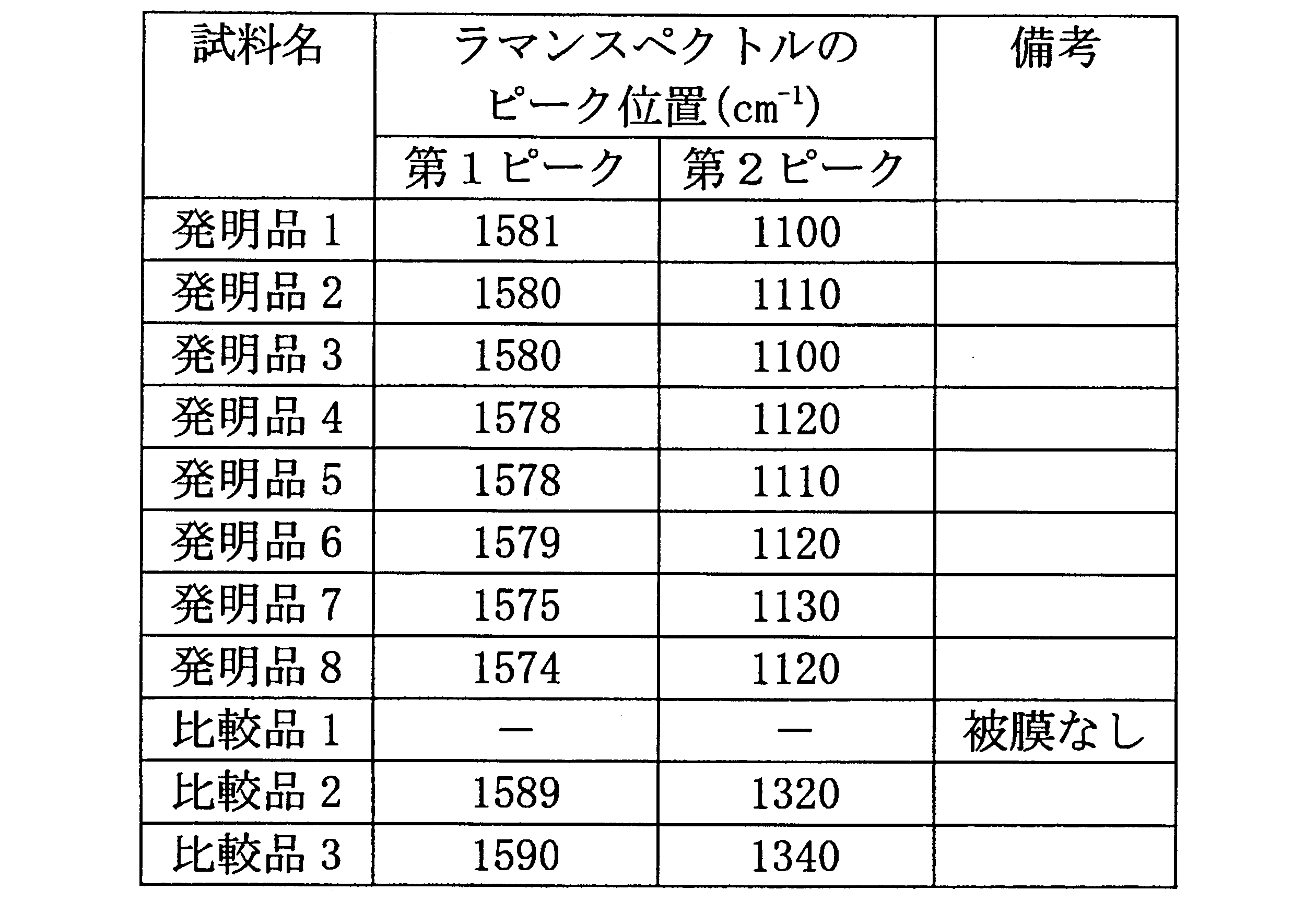
本発明の非晶質炭素膜は、514.5nmの波長を有するアルゴンガスレーザーを用いたラマン分光法によるラマンスペクトルにおいて、波数1560~1600cm-1の範囲内に第1ピークと、波数1100~1200cm-1の範囲内に第2ピークとを有することがより好ましい。波数800~2000cm-1の範囲でラマンスペクトルを測定したときに、波数1350cm-1付近にピークはほとんど見られず、上記波数の範囲内に第1ピークおよび第2ピークがあると、非晶質炭素膜の硬さが増加する傾向を示す。
本発明の非晶質炭素膜は、ダイヤモンドに匹敵する高い硬さを有し、切削工具として用いた場合、優れた耐摩耗性を発揮する。本発明の非晶質炭素膜はsp3結合の割合が高いので、常温硬さと高温硬さが高くなる。
本発明の非晶質炭素被覆工具の用途として、具体的には、ドリル、エンドミル、スローアウェイチップなどの切削工具、金型を挙げることができる。
本発明の非晶質炭素膜は、固体のカーボンを出発原料とした物理蒸着法により得られる。具体的な物理蒸着法としては、アークイオンプレーティング法、レーザーアブレーション法、スパッタリング法などを挙げることができる。その中でも、非晶質炭素膜と基材との密着性が高く、得られる非晶質炭素膜の硬さが高いアークイオンプレーティング法がより好ましい。アークイオンプレーティング法は、他の方式よりもイオン化率が高いカーボンイオンが生成するため、ダイヤモンド類似のsp3結合の比率が高く緻密で硬さの高い膜が得られ、耐摩耗性を大幅に向上させることができる。
アークイオンプレーティング法は、非晶質炭素膜の表面にマイクロパーティクルと呼ばれる突起物が生じやすい。マイクロパーティクルは耐摩耗性の低下や非晶質炭素膜の表面粗さを粗くし、被削材の表面品位を悪くする原因となる。アークイオンプレーティング法の中でも、マイクロパーティクルを低減させるフィルタードアークイオンプレティング法はより好ましい。
本発明の非晶質炭素膜を具体的に製造する方法としては以下を挙げることができる。工具形状の基材を成膜装置内に入れ、アルゴンプラズマにて基材の表面を洗浄する。次に、基材に-30~-300Vの直流電圧または-30~-500Vのパルス電圧の基材バイアス電圧をかけてC2H2およびCH4の1種または2種を5~20cm3/minの範囲の所定流量で炉内へ導入し、アーク放電電流80Aの陰極アーク放電によりグラファイトのターゲットを蒸発およびイオン化させることにより、基材に接する側に非晶質炭素膜の内層膜を被覆する。内層部の水素量に濃度勾配を持たせるためには、C2H2およびCH4の1種または2種の流量を時間とともに減少させるとよい。非晶質炭素膜の内層膜の被覆終了後、C2H2およびCH4の1種または2種を供給せずに非晶質炭素膜の外層部を被覆すると本発明の非晶質炭素被覆工具を得ることができる。
非晶質炭素膜の被覆時の基材温度は、50~200℃であると好ましく、50~150℃であるとより好ましい。基材温度が、200℃を超えると軟質なsp2結合のグラファイトが析出しやすくなり、50℃未満であると基材と非晶質炭素膜との密着性が低下する。本発明では、非晶質炭素膜の被覆時にはカーボンイオンが基材表面に照射され、非晶質炭素膜が形成されるので基材温度は上昇するため、基材を加熱ヒーターによって加熱しなくても基材温度が上昇する場合もある。
本発明の非晶質炭素被覆工具は、非晶質炭素膜と基材との密着性に優れるとともに耐摩耗性に優れる。本発明の非晶質炭素被覆工具は、高能率加工と工具寿命の長寿命化を実現し、被削材の仕上げ品位を良くすることが可能となる。
基材として、ドリル径φ0.3mm×長さ5.8mm(形状PRM030L-E)のプリント回路基板加工用超硬合金製ドリルを用意した。この基材をアークイオンプレーティング装置の炉内に入れた。加熱ヒーターを用いて基材を300℃まで加熱しながら、炉内を圧力1×10⁻⁴Paの真空にした。加熱ヒーターの設定温度を100℃まで下げて基材温度を150℃まで下げた後、アルゴンガスを導入し、圧力2×10⁻¹Paのアルゴン雰囲気に保持しながら、バイアス電源により基材取付治具に-400Vの基材バイアス電圧をかけてアルゴンプラズマにて基材表面を洗浄した。
次に、表1、2に示す条件にて基材の表面に非晶質炭素膜を形成した。表1は主にアークイオンプレーティング装置に関する条件を示し、表2は発明品5~8の基材のバイアス電圧に用いるパルス電圧条件を示す。発明品1~4については、基材のバイアス電圧として表1に示す直流電圧を用い、非晶質炭素膜の内層部の被覆開始時に5~15cm3/minの所定流量のC2H2を炉内に導入し、C2H2の流量を時間とともに徐々に減少し、非晶質炭素膜の内層部の被覆終了時にはC2H2の流量が0cm3/minになるように調節して内層部を被覆した。非晶質炭素膜の外層部はC2H2を炉内に供給せずに被覆した。発明品5~8については、基材のバイアス電圧として表2に示すパルス電圧を用い、非晶質炭素膜の内層部の被覆開始から被覆終了まで、一定流量のC2H2を供給して内層部を被覆した。非晶質炭素膜の外層部はC2H2を炉内に供給せずに被覆した。

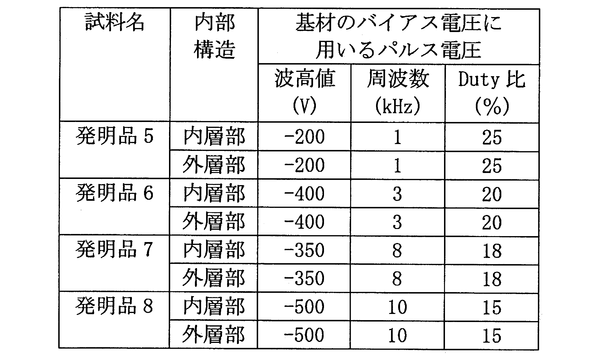
比較品1は被覆を行わない超硬合金製ドリルである。比較品2、3は、超硬合金製ドリルの基材をプラズマCVD装置内に入れ、アノード電圧100V、リフレクター電圧50V、フィラメント電流30Aを共通条件とし、表3に示す条件で基材の表面に非晶質炭素膜を形成した。

得られた発明品1~8、比較品2、3について、高エネルギーイオン(ヘリウムイオン)を入射粒子として用いた弾性反跳粒子検出法(ERDA)を使用して非晶質炭素膜の深さ方向の水素濃度分布を測定した。また、非晶質炭素膜の断面観察から走査型電子顕微鏡を用いて非晶質炭素膜の最大膜厚を測定した。それらの結果を表4に示した。
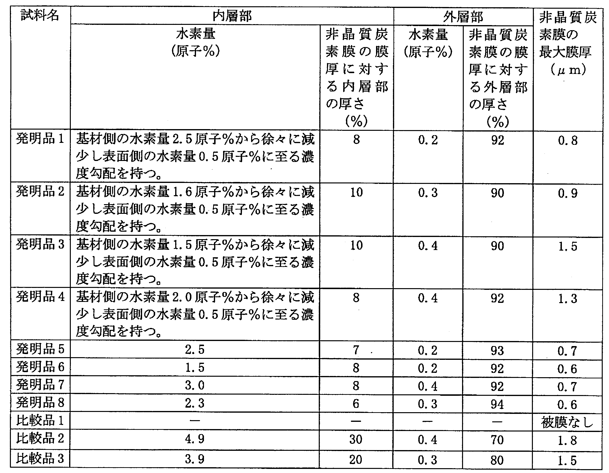
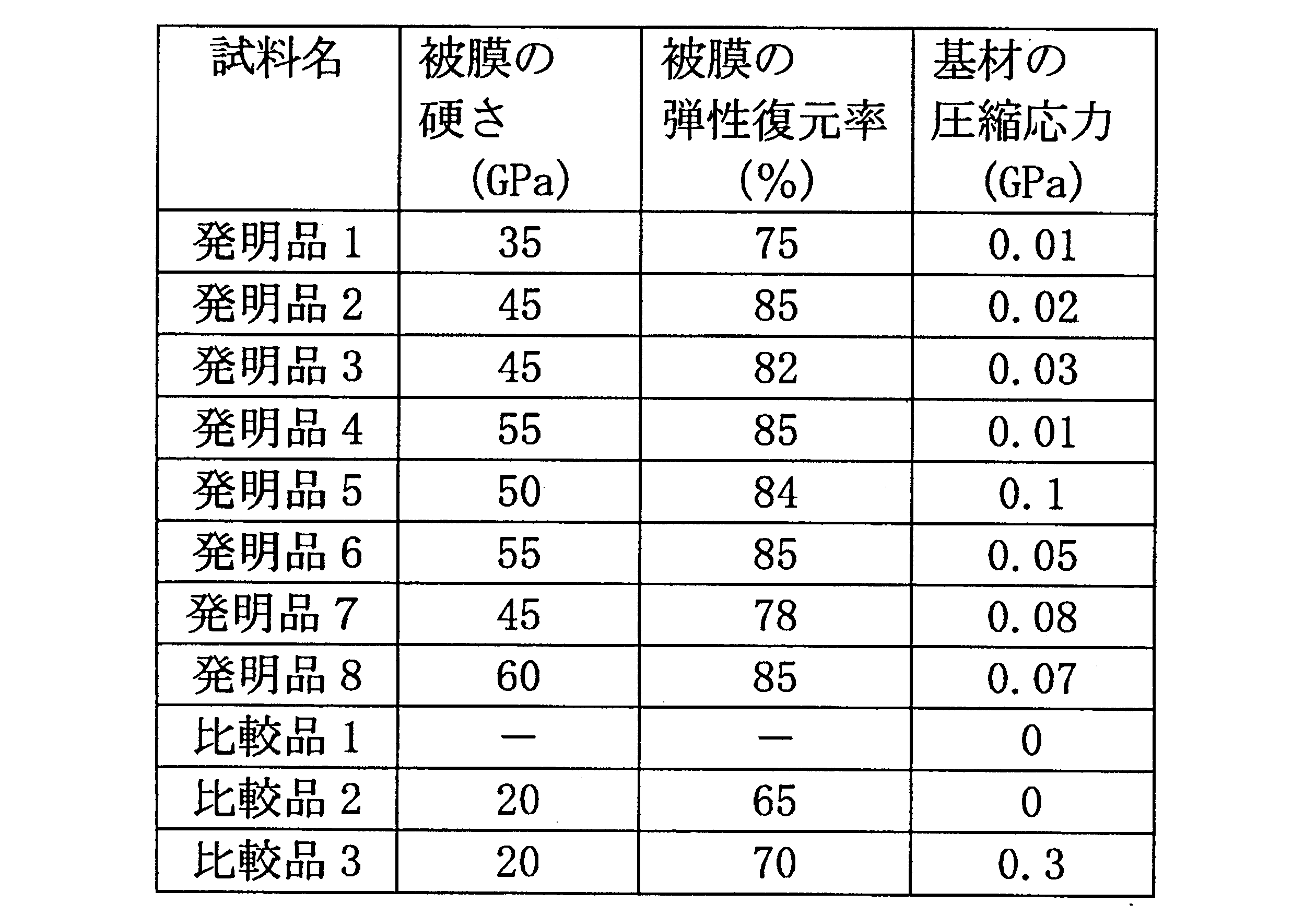
表4に示すように、外層部には0.5原子%未満の微量の水素が含まれるが、これは、炉内に残った水分などから混入したものと思われる。したがって、非晶質炭素膜の外層部は、実質的に水素を含有しないといえる。次にHysitron社製TriboIndentorを使用し、荷重1mNで非晶質炭素膜の硬さと弾性復元率を測定した。基材のWCに存在する圧縮応力を下記の応力測定条件で測定した。これらの結果を表5に示した。
[応力測定条件]
測定装置: 株式会社リガク製微小部応力測定装置
X線管球: Cuターゲット
コリメータ: φ2mm
X線出力: 30kV,20mA
標準ブラック角2θ0: 117度(WC(211)面)
ψ: 0度、17度、24度、30度、35度、40度の6点測定
ポアッソン比υ: 0.19
ヤング率E: 700GPa
測定装置: 株式会社リガク製微小部応力測定装置
X線管球: Cuターゲット
コリメータ: φ2mm
X線出力: 30kV,20mA
標準ブラック角2θ0: 117度(WC(211)面)
ψ: 0度、17度、24度、30度、35度、40度の6点測定
ポアッソン比υ: 0.19
ヤング率E: 700GPa
514.5nmの波長を持つアルゴンガスレーザーのラマン分光測定装置を用いて、発明品1~8と比較品2,3の非晶質炭素膜のラマンスペクトルを測定した。これらの結果を表6に示した。
得られたドリルについて、穴あけ試験を行い、切刃における凝着状況と摩耗状態を測定した。これらの結果を表7に示した。
[穴あけ試験]
ドリル径: φ0.3mm
被削材: プリント回路基板FR-4(4層板)×2枚重ね
回転数: 120000回転/min、
テーブル送り速度: 3.0m/min
1回転当たりの送り量: 25μm/rev
加工数: 3000穴を加工する。
ドリル径: φ0.3mm
被削材: プリント回路基板FR-4(4層板)×2枚重ね
回転数: 120000回転/min、
テーブル送り速度: 3.0m/min
1回転当たりの送り量: 25μm/rev
加工数: 3000穴を加工する。
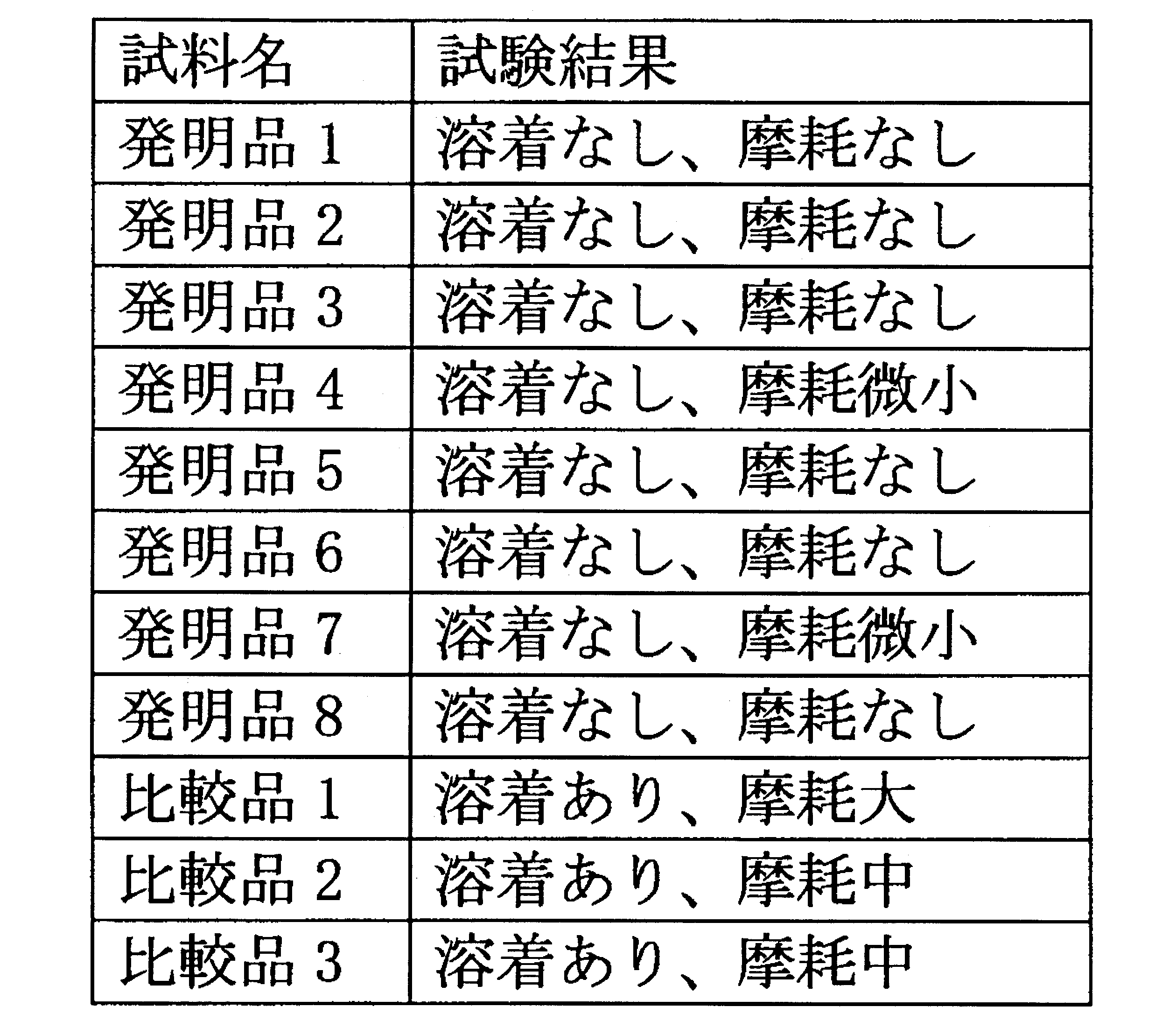
本発明品は、比較品に比べて、優れた耐溶着性と耐摩耗性を備えることがわかる。従って、穴あけ加工後の穴加工精度も非常に高く、長寿命化が可能になる。
基材として、フライス用スローアウェイチップ(K10相当超硬合金、形番AECW16T3PEFR)を用意した。この基材をアークイオンプレーティング装置の炉内に入れた。加熱ヒーターを用いて基材を300℃まで加熱しながら炉内を圧力1×10⁻⁴Paの真空にした。加熱ヒーターの設定温度を100℃まで下げて基材温度を150℃まで下げた後、アルゴンガスを導入し、圧力2×10⁻¹Paのアルゴン雰囲気に保持しながら、バイアス電源により基材取付治具に-400Vの基材バイアス電圧をかけてアルゴンプラズマにて基材の表面を洗浄した。
次に、表8、9に示す条件にて基材の表面に非晶質炭素膜を形成した。表8は主にアークイオンプレーティング装置に関する条件を示し、表9は基材のバイアス電圧に用いるパルス電圧条件を示す。発明品9~12については、非晶質炭素膜の内層部の被覆開始時に6~12cm3/minの所定流量のC2H2を炉内に導入し、C2H2の流量を時間とともに徐々に減少させ、非晶質炭素膜の内層部の被覆終了時にはC2H2の流量が0cm3/minになるように調節して内層部を被覆した。非晶質炭素膜の外層部はC2H2を炉内に供給せずに被覆した。発明品13~16については、非晶質炭素膜の内層部の被覆開始から被覆終了まで、一定流量のC2H2を供給して内層部を被覆した。非晶質炭素膜の外層部はC2H2を炉内に供給せずに被覆した。
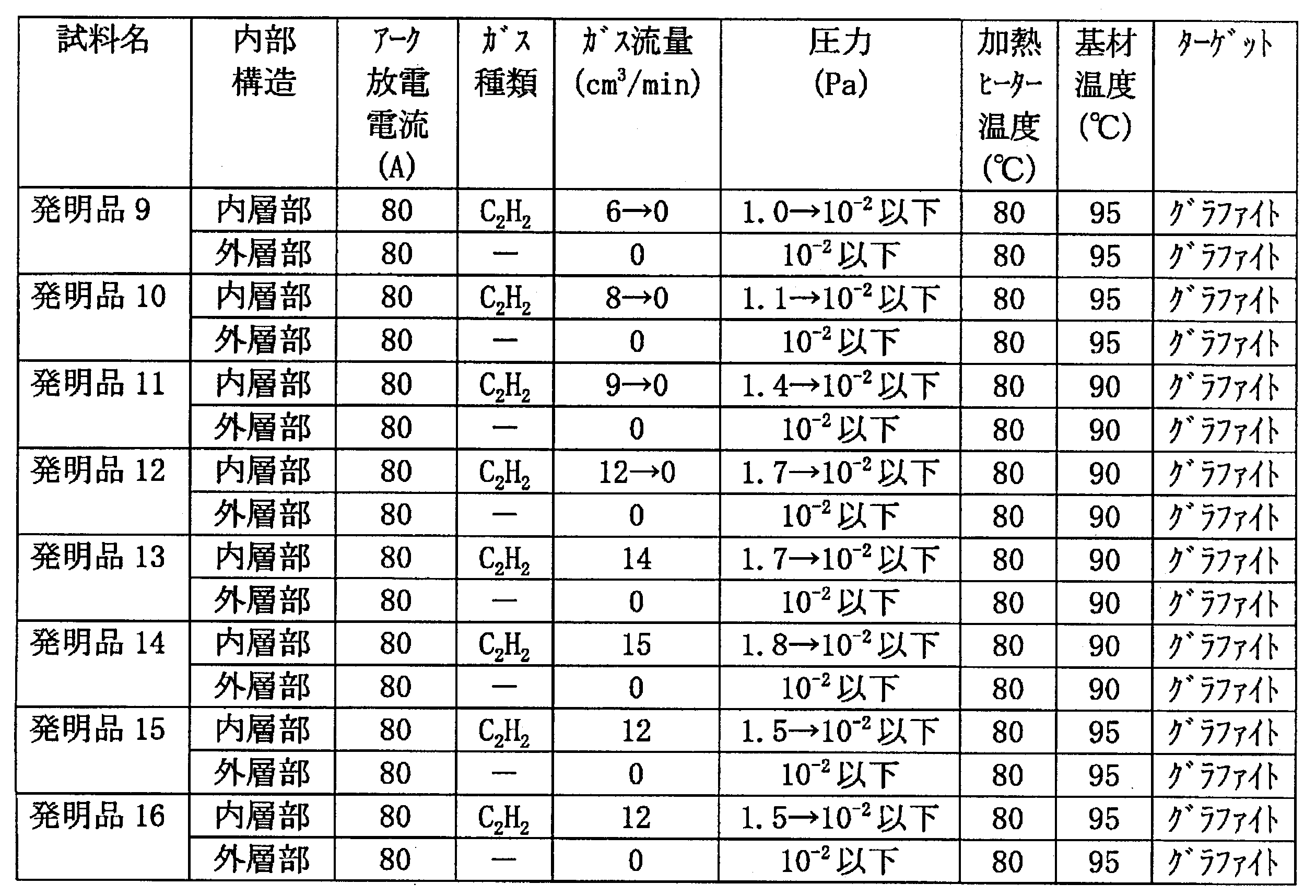

比較品4は被覆を行わない超硬合金製スローアウェイチップである。比較品5は、基材をプラズマCVD成膜装置の炉内に入れ、ベンゼンC6H6の流量10cm3/min、圧力4.3×10-1Pa、基材温度200℃、基材のバイアス電圧-1500V(直流電圧)という条件で基材の表面に非晶質炭素膜を形成した。
得られた発明品9~16、比較品5について、高エネルギーイオン(ヘリウムイオン)を入射粒子として用いた弾性反跳粒子検出法(ERDA)を使用して非晶質炭素膜の深さ方向の水素濃度分布を測定した。また、非晶質炭素膜の断面観察から走査型電子顕微鏡を用いて非晶質炭素膜の最大膜厚を測定した。それらの結果を表10に示した。

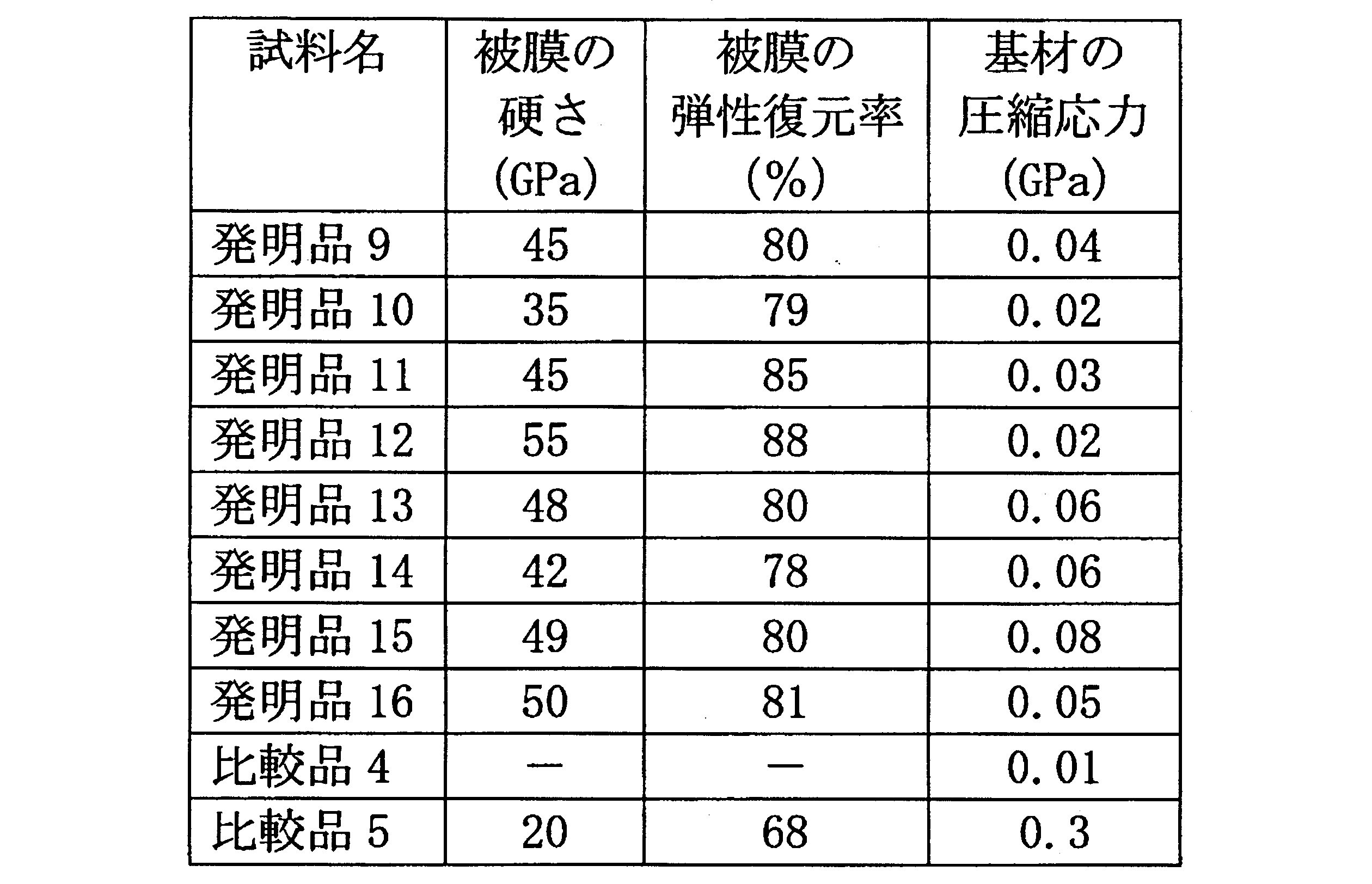
表10に示すように、外層部には0.5原子%未満の微量の水素が含まれるが、これは、炉内に残った水分などから混入したものと思われる。Hysitron社製TriboIndentorを使用し、実施例1と同様な条件で非晶質炭素膜の硬さと弾性復元率を測定した。基材のWCに存在する圧縮応力を実施例1と同様な条件で測定した。これらの結果を表11に示した。
514.5nmの波長を持つアルゴンガスレーザーのラマン分光測定装置を用いて、発明品9~16と比較品5の非晶質炭素膜のラマンスペクトルを測定した。これらの結果を表12に示した。

得られたスローアウェイチップについて、フライス加工試験を行い、切刃における凝着状況と摩耗状態を測定した。 これらの結果を表13に示した。
[フライス加工試験]
被削材: アルミニウム合金ADC12
チップ形状: AECW16T3PEFR
切削速度: V=300m/min
切り込み: Ad=5mm
送り: f=0.15mm/rev
ダウンカット
被削材: アルミニウム合金ADC12
チップ形状: AECW16T3PEFR
切削速度: V=300m/min
切り込み: Ad=5mm
送り: f=0.15mm/rev
ダウンカット
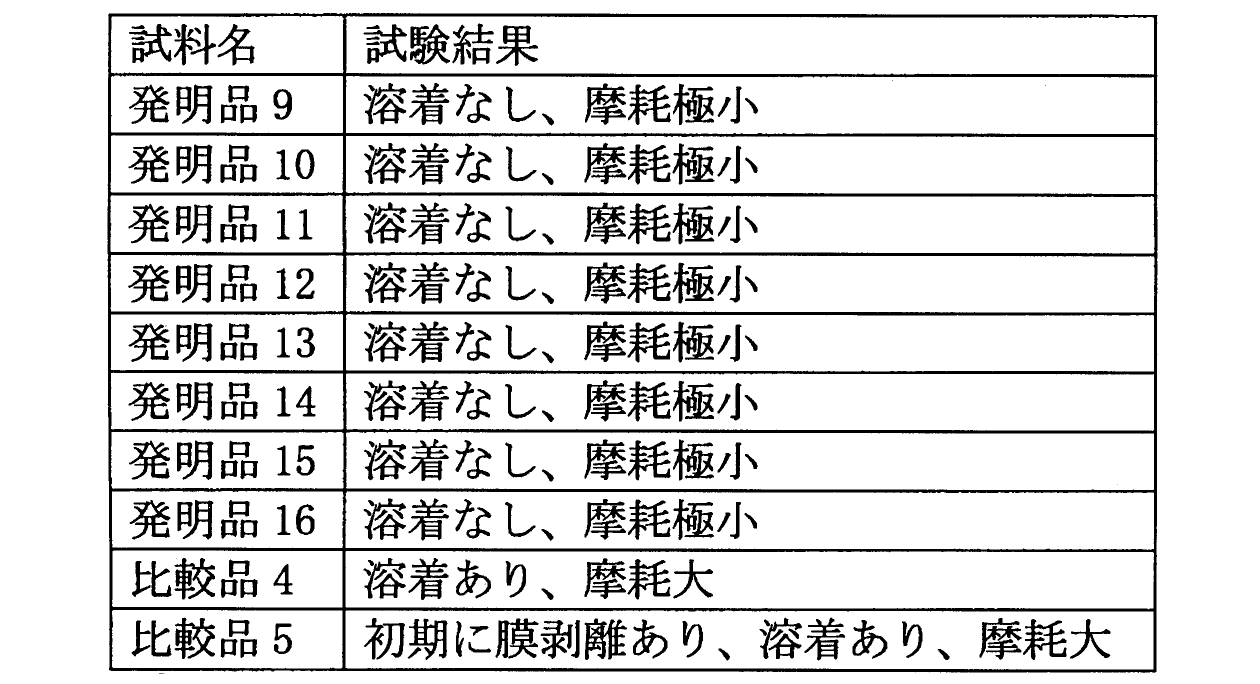
本発明品の非晶質炭素被覆工具は、比較品に比べて、被膜と基材との密着性に優れ、優れた耐溶着性と耐摩耗性を備えることがわかる。そのため長寿命化が可能になる。そのため、本発明の非晶質炭素被覆工具は産業上の利用可能性の高い発明である。
Claims (9)
- 基材と非晶質炭素膜とを備え、非晶質炭素膜は基材に接する側の内層部と表面側の外層部とからなり、非晶質炭素膜の内層部に含まれる水素量が、非晶質炭素膜の外層部に含まれる水素量よりも多い、ことを特徴とする非晶質炭素被覆工具。
- 非晶質炭素膜の内層部が、基材に接する側から表面側に向けて徐々に減少する水素濃度勾配を有する、請求項1に記載の非晶質炭素被覆工具。
- 非晶質炭素膜が、内層部に0.5~3原子%の水素量と、外層部に0.5原子%未満の水素量とを有する、請求項1または2に記載の非晶質炭素被覆工具。
- 非晶質炭素膜が、非晶質炭素膜の膜厚全体の1~10%の内層部の厚さと90~99%の外層部の厚さとを有する、請求項1~3のいずれか1項に記載の非晶質炭素被覆工具。
- 非晶質炭素膜が膜厚0.06~5μmを有する、請求項1~4のいずれか1項に記載の非晶質炭素被覆工具。
- 非晶質炭素膜が、ナノインデンテーション法による硬さ20~100GPaを有する、請求項1~5のいずれか1項に記載の非晶質炭素被覆工具。
- 非晶質炭素膜が、弾性復元率70~100%を有する、請求項1~6のいずれか1項に記載の非晶質炭素被覆工具。
- 基材に存在する圧縮応力が0.3GPa以下である、請求項1~7のいずれか1項に記載の非晶質炭素被覆工具。
- 非晶質炭素膜が、514.5nmの波長を有するアルゴンガスレーザーを用いたラマン分光法によるラマンスペクトルにおいて、波数1560~1600cm-1の範囲内の第1ピークと、波数1100~1200cm-1の範囲内の第2ピークとを有する、請求項1~8のいずれか1項に記載の非晶質炭素被覆工具。
Applications Claiming Priority (2)
| Application Number | Priority Date | Filing Date | Title |
|---|---|---|---|
| JP2008-068676 | 2008-03-18 | ||
| JP2008068676A JP5176621B2 (ja) | 2008-03-18 | 2008-03-18 | 非晶質炭素被覆工具 |
Publications (1)
| Publication Number | Publication Date |
|---|---|
| WO2009116552A1 true WO2009116552A1 (ja) | 2009-09-24 |
Family
ID=41090952
Family Applications (1)
| Application Number | Title | Priority Date | Filing Date |
|---|---|---|---|
| PCT/JP2009/055228 Ceased WO2009116552A1 (ja) | 2008-03-18 | 2009-03-18 | 非晶質炭素被覆工具 |
Country Status (2)
| Country | Link |
|---|---|
| JP (1) | JP5176621B2 (ja) |
| WO (1) | WO2009116552A1 (ja) |
Cited By (4)
| Publication number | Priority date | Publication date | Assignee | Title |
|---|---|---|---|---|
| JP2011104687A (ja) * | 2009-11-16 | 2011-06-02 | Mitsubishi Materials Corp | 耐剥離性と耐摩耗性にすぐれたダイヤモンド被覆工具 |
| CN105420670A (zh) * | 2014-09-12 | 2016-03-23 | 株式会社神户制钢所 | 硬质滑动部件的制造方法 |
| US9546425B2 (en) | 2010-01-19 | 2017-01-17 | Kabushiki Kaisha Riken | Member having hydrogen-containing, hard, amorphous carbon coating and its production method |
| CN106604796A (zh) * | 2014-09-03 | 2017-04-26 | 三菱综合材料株式会社 | 表面包覆切削工具及其制造方法 |
Families Citing this family (7)
| Publication number | Priority date | Publication date | Assignee | Title |
|---|---|---|---|---|
| JP6039479B2 (ja) * | 2013-03-25 | 2016-12-07 | 京セラ株式会社 | 表面被覆部材 |
| JP6103040B2 (ja) * | 2013-03-29 | 2017-03-29 | 日立金属株式会社 | 被覆工具の製造方法 |
| JP6200343B2 (ja) * | 2014-02-10 | 2017-09-20 | 大同メタル工業株式会社 | 摺動部材 |
| JP6612864B2 (ja) * | 2015-05-28 | 2019-11-27 | 京セラ株式会社 | 切削工具 |
| JP7067690B2 (ja) * | 2020-04-24 | 2022-05-16 | 住友電工ハードメタル株式会社 | 切削工具 |
| US11992882B2 (en) | 2020-04-24 | 2024-05-28 | Sumitomo Electric Hardmetal Corp. | Cutting tool |
| JP7023388B1 (ja) * | 2020-04-24 | 2022-02-21 | 住友電工ハードメタル株式会社 | 切削工具 |
Citations (7)
| Publication number | Priority date | Publication date | Assignee | Title |
|---|---|---|---|---|
| JPH09314405A (ja) * | 1996-05-31 | 1997-12-09 | Kyocera Corp | 被覆切削工具 |
| JPH1082390A (ja) * | 1996-07-18 | 1998-03-31 | Sanyo Electric Co Ltd | 摺動部材、圧縮機及び回転圧縮機 |
| JP2003251503A (ja) * | 2001-12-26 | 2003-09-09 | Sumitomo Electric Ind Ltd | 表面被覆切削工具 |
| JP2005008851A (ja) * | 2003-05-29 | 2005-01-13 | Nissan Motor Co Ltd | 硬質炭素薄膜付き機械加工工具用切削油及び硬質炭素薄膜付き機械加工工具 |
| JP2005022073A (ja) * | 2003-06-11 | 2005-01-27 | Sumitomo Electric Hardmetal Corp | Dlc被覆工具 |
| JP2005281727A (ja) * | 2004-03-26 | 2005-10-13 | Kurita Seisakusho:Kk | Dlc成膜物の製造方法およびdlc成膜物 |
| JP2007126754A (ja) * | 2006-12-21 | 2007-05-24 | Nissin Electric Co Ltd | 真空アーク蒸着装置 |
Family Cites Families (3)
| Publication number | Priority date | Publication date | Assignee | Title |
|---|---|---|---|---|
| JPH01201095A (ja) * | 1988-02-04 | 1989-08-14 | Idemitsu Petrochem Co Ltd | ダイヤモンド状炭素膜とその製造方法 |
| JPH0665745A (ja) * | 1992-08-24 | 1994-03-08 | Sumitomo Electric Ind Ltd | ダイヤモンド被覆硬質材料およびその製造法 |
| JP4776395B2 (ja) * | 2006-02-24 | 2011-09-21 | 京セラ株式会社 | 切削工具 |
-
2008
- 2008-03-18 JP JP2008068676A patent/JP5176621B2/ja active Active
-
2009
- 2009-03-18 WO PCT/JP2009/055228 patent/WO2009116552A1/ja not_active Ceased
Patent Citations (7)
| Publication number | Priority date | Publication date | Assignee | Title |
|---|---|---|---|---|
| JPH09314405A (ja) * | 1996-05-31 | 1997-12-09 | Kyocera Corp | 被覆切削工具 |
| JPH1082390A (ja) * | 1996-07-18 | 1998-03-31 | Sanyo Electric Co Ltd | 摺動部材、圧縮機及び回転圧縮機 |
| JP2003251503A (ja) * | 2001-12-26 | 2003-09-09 | Sumitomo Electric Ind Ltd | 表面被覆切削工具 |
| JP2005008851A (ja) * | 2003-05-29 | 2005-01-13 | Nissan Motor Co Ltd | 硬質炭素薄膜付き機械加工工具用切削油及び硬質炭素薄膜付き機械加工工具 |
| JP2005022073A (ja) * | 2003-06-11 | 2005-01-27 | Sumitomo Electric Hardmetal Corp | Dlc被覆工具 |
| JP2005281727A (ja) * | 2004-03-26 | 2005-10-13 | Kurita Seisakusho:Kk | Dlc成膜物の製造方法およびdlc成膜物 |
| JP2007126754A (ja) * | 2006-12-21 | 2007-05-24 | Nissin Electric Co Ltd | 真空アーク蒸着装置 |
Cited By (6)
| Publication number | Priority date | Publication date | Assignee | Title |
|---|---|---|---|---|
| JP2011104687A (ja) * | 2009-11-16 | 2011-06-02 | Mitsubishi Materials Corp | 耐剥離性と耐摩耗性にすぐれたダイヤモンド被覆工具 |
| US9546425B2 (en) | 2010-01-19 | 2017-01-17 | Kabushiki Kaisha Riken | Member having hydrogen-containing, hard, amorphous carbon coating and its production method |
| CN106604796A (zh) * | 2014-09-03 | 2017-04-26 | 三菱综合材料株式会社 | 表面包覆切削工具及其制造方法 |
| CN106604796B (zh) * | 2014-09-03 | 2018-12-04 | 三菱综合材料株式会社 | 表面包覆切削工具及其制造方法 |
| US10358712B2 (en) | 2014-09-03 | 2019-07-23 | Mitsubishi Materials Corporation | Surface-coated cutting tool and method of manufacturing the same |
| CN105420670A (zh) * | 2014-09-12 | 2016-03-23 | 株式会社神户制钢所 | 硬质滑动部件的制造方法 |
Also Published As
| Publication number | Publication date |
|---|---|
| JP5176621B2 (ja) | 2013-04-03 |
| JP2009220238A (ja) | 2009-10-01 |
Similar Documents
| Publication | Publication Date | Title |
|---|---|---|
| JP5176621B2 (ja) | 非晶質炭素被覆工具 | |
| KR101255430B1 (ko) | 표면 피복 절삭 공구 | |
| JP7032579B1 (ja) | 切削工具 | |
| JP4704335B2 (ja) | 表面被覆切削工具 | |
| JP2005262389A (ja) | チタン合金加工用表面被覆切削工具 | |
| KR101079902B1 (ko) | 표면 피복 절삭 공구 | |
| WO2014142190A1 (ja) | 硬質皮膜、硬質皮膜被覆部材、及びそれらの製造方法 | |
| JP5590331B2 (ja) | 耐摩耗性と切屑排出性に優れた表面被覆ドリル | |
| KR101082655B1 (ko) | 표면 피복 절삭 공구 | |
| JP2007260851A (ja) | 表面被覆切削工具 | |
| JP4445815B2 (ja) | 表面被覆切削工具 | |
| US12049693B2 (en) | Cutting tool | |
| WO2018230212A1 (ja) | 表面被覆切削工具 | |
| JP5464494B2 (ja) | 硬質被覆層の耐欠損性、耐剥離性に優れる表面被覆切削工具 | |
| JP5327534B2 (ja) | 硬質被覆層の耐欠損性、耐剥離性に優れる表面被覆切削工具 | |
| US20230123968A1 (en) | Cutting tool | |
| JP6930446B2 (ja) | 硬質皮膜、硬質皮膜被覆工具及びその製造方法 | |
| JP5672444B2 (ja) | 耐摩耗性と切屑排出性に優れた表面被覆ドリル | |
| JP7286812B2 (ja) | 切削工具 | |
| JP2011156639A (ja) | 硬質被覆層がすぐれた耐欠損性を発揮する表面被覆切削工具 | |
| JP2008100301A (ja) | ダイヤモンド被覆切削インサート及び切削工具 | |
| JP2005271132A (ja) | 表面被覆切削工具 | |
| JP5267790B2 (ja) | 表面被覆切削工具 | |
| JP2005262386A (ja) | 表面被覆切削工具 | |
| JP2006082177A (ja) | 非晶質カーボン被覆工具及び非晶質カーボン皮膜の被覆方法 |
Legal Events
| Date | Code | Title | Description |
|---|---|---|---|
| 121 | Ep: the epo has been informed by wipo that ep was designated in this application |
Ref document number: 09723308 Country of ref document: EP Kind code of ref document: A1 |
|
| NENP | Non-entry into the national phase |
Ref country code: DE |
|
| 122 | Ep: pct application non-entry in european phase |
Ref document number: 09723308 Country of ref document: EP Kind code of ref document: A1 |