WO2009081968A1 - 金属酸化物半導体の製造方法およびこれを用いる半導体素子 - Google Patents
金属酸化物半導体の製造方法およびこれを用いる半導体素子 Download PDFInfo
- Publication number
- WO2009081968A1 WO2009081968A1 PCT/JP2008/073539 JP2008073539W WO2009081968A1 WO 2009081968 A1 WO2009081968 A1 WO 2009081968A1 JP 2008073539 W JP2008073539 W JP 2008073539W WO 2009081968 A1 WO2009081968 A1 WO 2009081968A1
- Authority
- WO
- WIPO (PCT)
- Prior art keywords
- metal oxide
- metal
- oxide semiconductor
- thin film
- semiconductor
- Prior art date
- Legal status (The legal status is an assumption and is not a legal conclusion. Google has not performed a legal analysis and makes no representation as to the accuracy of the status listed.)
- Ceased
Links
Images
Classifications
-
- H—ELECTRICITY
- H10—SEMICONDUCTOR DEVICES; ELECTRIC SOLID-STATE DEVICES NOT OTHERWISE PROVIDED FOR
- H10D—INORGANIC ELECTRIC SEMICONDUCTOR DEVICES
- H10D30/00—Field-effect transistors [FET]
- H10D30/60—Insulated-gate field-effect transistors [IGFET]
- H10D30/67—Thin-film transistors [TFT]
- H10D30/674—Thin-film transistors [TFT] characterised by the active materials
- H10D30/6755—Oxide semiconductors, e.g. zinc oxide, copper aluminium oxide or cadmium stannate
-
- H—ELECTRICITY
- H10—SEMICONDUCTOR DEVICES; ELECTRIC SOLID-STATE DEVICES NOT OTHERWISE PROVIDED FOR
- H10P—GENERIC PROCESSES OR APPARATUS FOR THE MANUFACTURE OR TREATMENT OF DEVICES COVERED BY CLASS H10
- H10P14/00—Formation of materials, e.g. in the shape of layers or pillars
- H10P14/20—Formation of materials, e.g. in the shape of layers or pillars of semiconductor materials
- H10P14/26—Formation of materials, e.g. in the shape of layers or pillars of semiconductor materials using liquid deposition
- H10P14/265—Formation of materials, e.g. in the shape of layers or pillars of semiconductor materials using liquid deposition using solutions
-
- H—ELECTRICITY
- H10—SEMICONDUCTOR DEVICES; ELECTRIC SOLID-STATE DEVICES NOT OTHERWISE PROVIDED FOR
- H10P—GENERIC PROCESSES OR APPARATUS FOR THE MANUFACTURE OR TREATMENT OF DEVICES COVERED BY CLASS H10
- H10P14/00—Formation of materials, e.g. in the shape of layers or pillars
- H10P14/20—Formation of materials, e.g. in the shape of layers or pillars of semiconductor materials
- H10P14/34—Deposited materials, e.g. layers
- H10P14/3402—Deposited materials, e.g. layers characterised by the chemical composition
- H10P14/3424—Deposited materials, e.g. layers characterised by the chemical composition being Group IIB-VIA materials
- H10P14/3426—Oxides
-
- H—ELECTRICITY
- H10—SEMICONDUCTOR DEVICES; ELECTRIC SOLID-STATE DEVICES NOT OTHERWISE PROVIDED FOR
- H10P—GENERIC PROCESSES OR APPARATUS FOR THE MANUFACTURE OR TREATMENT OF DEVICES COVERED BY CLASS H10
- H10P14/00—Formation of materials, e.g. in the shape of layers or pillars
- H10P14/20—Formation of materials, e.g. in the shape of layers or pillars of semiconductor materials
- H10P14/34—Deposited materials, e.g. layers
- H10P14/3402—Deposited materials, e.g. layers characterised by the chemical composition
- H10P14/3434—Deposited materials, e.g. layers characterised by the chemical composition being oxide semiconductor materials
-
- H—ELECTRICITY
- H10—SEMICONDUCTOR DEVICES; ELECTRIC SOLID-STATE DEVICES NOT OTHERWISE PROVIDED FOR
- H10P—GENERIC PROCESSES OR APPARATUS FOR THE MANUFACTURE OR TREATMENT OF DEVICES COVERED BY CLASS H10
- H10P14/00—Formation of materials, e.g. in the shape of layers or pillars
- H10P14/20—Formation of materials, e.g. in the shape of layers or pillars of semiconductor materials
- H10P14/38—Formation of materials, e.g. in the shape of layers or pillars of semiconductor materials characterised by treatments done after the formation of the materials
- H10P14/3802—Crystallisation or recrystallisation of non-monocrystalline semiconductor materials, e.g. regrowth
-
- H—ELECTRICITY
- H10—SEMICONDUCTOR DEVICES; ELECTRIC SOLID-STATE DEVICES NOT OTHERWISE PROVIDED FOR
- H10P—GENERIC PROCESSES OR APPARATUS FOR THE MANUFACTURE OR TREATMENT OF DEVICES COVERED BY CLASS H10
- H10P14/00—Formation of materials, e.g. in the shape of layers or pillars
- H10P14/20—Formation of materials, e.g. in the shape of layers or pillars of semiconductor materials
- H10P14/29—Formation of materials, e.g. in the shape of layers or pillars of semiconductor materials characterised by the substrates
- H10P14/2901—Materials
Definitions
- the present invention relates to a method of manufacturing a metal oxide semiconductor in which post-heating is performed after the formation of the metal oxide semiconductor, and a semiconductor element using the same.
- a metal oxide semiconductor and a thin film transistor (TFT) element using the metal oxide semiconductor are well known.
- a metal oxide semiconductor is formed by sputtering, or, for example, a metal film formed on a substrate, a metal salt, an organic metal, or the like is decomposed and oxidized by thermal oxidation, plasma oxidation, or the like.
- a method of converting to is also known.
- Non-Patent Documents 1 and 2 As for the obtained semiconductor film, it has been reported that post-baking at 300 ° C. or higher for about 30 minutes is necessary for performance stabilization, for example, performance does not appear immediately after film formation or performance variation is large. .
- the film can be formed at about room temperature, in order to obtain stable performance at the product level, it is exposed to a high temperature of 300 ° C. or higher, so that it is substantially difficult to apply to a resin substrate.
- Non-Patent Documents 3 and 4 the performance as a metal oxide semiconductor is derived from a metal chloride precursor by treatment at 600 ° C., but the performance required by itself alone may not be obtained even by heat treatment at a high temperature for a long time. Many.
- an object of the present invention is to use a microwave for post-heating in the production of a metal oxide semiconductor, so that a metal oxide semiconductor having stable and excellent semiconductor performance does not require a high process temperature. It is in providing a manufacturing method of high productivity.
- a method for manufacturing a metal oxide semiconductor comprising performing post-heating by irradiating microwaves after forming the metal oxide semiconductor.
- a semiconductor element comprising a metal oxide semiconductor produced by the method for producing a metal oxide semiconductor according to any one of 1 to 7.
- a metal oxide semiconductor in the production of a metal oxide semiconductor layer, by using microwaves for post-baking, a metal oxide semiconductor can be formed without requiring a high process temperature.
- the metal oxide semiconductor layer or precursor thin film can be formed by sputtering or coating.
- microwaves are used for both baking and post-baking.
- a metal oxide semiconductor can be formed without requiring a substantially high process temperature.
- the processing time can be shortened at a lower temperature by selecting a nitrate precursor.
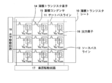
- FIG. 1 is a schematic equivalent circuit diagram of an example of a thin film transistor sheet 10 which is an electronic device in which a plurality of thin film transistor elements are arranged. It is a schematic sectional drawing of the produced thin-film transistor element. It is a schematic sectional drawing of the produced thin-film transistor element.
- the present invention after formation of a metal oxide semiconductor, microwave irradiation is performed and post-heating (post-bake) is performed, so that the carrier mobility of the metal oxide semiconductor, the on / off value when a TFT element is formed, and the like.
- the present invention relates to a method for manufacturing a metal oxide semiconductor that achieves improved performance.
- Examples of the metal oxide semiconductor include those composed of metal oxides containing the following metal atoms.
- a thin film of a metal oxide semiconductor containing a single metal atom or a plurality of metal atoms selected from the aforementioned metal atoms is produced by the method of the present invention.
- the metal oxide semiconductor any state of single crystal, polycrystal, and amorphous can be used, but an amorphous thin film is preferably used.
- the metal oxide semiconductor preferably contains any of indium, tin, and zinc, and may be used in combination. Moreover, it is preferable that a gallium or aluminum is included as another metal.
- the electron carrier concentration of the metal oxide semiconductor according to the present invention is less than 10 18 / cm 3 .
- This carrier concentration is a value when measured at room temperature.
- the room temperature is, for example, 25 ° C., specifically, a certain temperature appropriately selected from the range of about 0 ° C. to 40 ° C.
- the electron carrier concentration of the amorphous oxide according to the present invention does not need to satisfy less than 10 18 / cm 3 in the entire range of 0 ° C. to 40 ° C.
- a carrier electron density of less than 10 18 / cm 3 may be realized at 25 ° C.
- further lowering the electron carrier concentration, 10 17 / cm 3 or less normally-off of the TFT is obtained good yield when more preferably 10 16 / cm 3 or less.
- the measurement of electron carrier concentration can be obtained by Hall effect measurement.
- the film thickness of the semiconductor that is a metal oxide is not particularly limited, but the characteristics of the obtained transistor are often greatly influenced by the film thickness of the semiconductor film, and the film thickness varies depending on the semiconductor. Generally, it is 1 ⁇ m or less, preferably 1 to 300 nm, more preferably 5 to 200 nm, and still more preferably 10 to 100 nm.
- the composition of the precursor material or target of the metal oxide semiconductor, the manufacturing (film formation) conditions, and the like are controlled, for example, the electron carrier concentration is 10 12 / cm 3 or more and 10 18 / cm 3. Less than. More preferably, it is in the range of 10 13 / cm 3 or more and 10 17 / cm 3 or less, and more preferably 10 15 / cm 3 or more and 10 16 / cm 3 or less.
- these metal oxide semiconductors can be formed at a temperature of about room temperature by precisely controlling the atmosphere during film formation by sputtering. A film can be deposited on the substrate.
- heat treatment at 300 ° C. or higher is performed as a post-treatment for stabilization. And stabilize.
- post-baking treatment is thought to optimize carrier density and bands by some action, the mechanism of action is not clear.
- the present invention is characterized in that microwave irradiation is performed as post-baking treatment on the metal oxide semiconductor film once formed.
- the method for manufacturing the metal oxide semiconductor is not particularly limited.
- microwave irradiation is performed as post-baking treatment, heat treatment for a long time at a high temperature of 300 ° C. or higher is not required, and the temperature can be lowered and the treatment time can be shortened.
- the conventional post-baking process requires a high temperature of 300 ° C. or higher, so that the substrate is deformed and deteriorated, which is difficult to apply.
- microwave irradiation causes damage to the substrate. Can be implemented without
- microwave irradiation In the present invention, microwave (0.3 GHz to 50 GHz) irradiation is used as the post-bake treatment. In the present invention, after a metal oxide semiconductor or a metal oxide thin film serving as a precursor thereof is formed, the thin film is irradiated with electromagnetic waves, particularly microwaves (frequency 0.3 GHz to 50 GHz), and post-baked. I do.
- the post-bake temperature in the present invention is preferably 300 ° C. or lower, and more preferably 250 ° C. or lower from the viewpoint of application to a machine resin substrate having low heat resistance. Even if a temperature higher than 300 ° C. is used, the stabilization effect is already in the saturation region, so that the energy efficiency for stabilization is impaired.
- the metal oxide semiconductor thin film By irradiating the metal oxide semiconductor thin film with microwaves, electrons in the metal oxide vibrate, Joule heat is generated, and the thin film is uniformly heated from the inside. Since a substrate such as glass or resin has almost no absorption in the microwave region, the semiconductor substrate itself hardly generates heat, and only the semiconductor thin film portion can be selectively heated.
- microwave heating In microwave heating, microwave absorption concentrates on strongly absorbing substances and can be raised to 500-600 ° C. in a very short time. Therefore, when this method is used in the present invention, The substrate itself is not affected by heating by electromagnetic waves, and only the thin film can be baked and heated to the post-bake temperature in a short time. Although it depends on the metal oxide semiconductor material and the substrate material, the heating temperature and heating time in post-baking can be controlled by the microwave output and irradiation time, and any temperature and time can be selected. However, from the viewpoint of using a resin substrate having a heat resistance of 300 ° C. or lower and low heat resistance, the surface of the thin film is preferably adjusted to a temperature of 250 ° C. or lower.
- the temperature of the thin film surface, the temperature of the substrate, etc. can be measured by a surface thermometer using a thermocouple or a non-contact surface thermometer.
- the time for heating the precursor material can be set arbitrarily, but is preferably in the range of 1 second to 60 minutes from the viewpoint of the characteristics of the electronic device and production efficiency. More preferably, it is 5 minutes to 30 minutes.
- the microwave refers to an electromagnetic wave having a frequency of 0.3 GHz to 50 GHz, and is used in 0.8 MHz and 1.5 GHz band, 2 GHz band, amateur radio, aircraft radar, etc. used in mobile communication. .2 GHz band, microwave oven, private radio, 2.4 GHz band used for VICS, 3 GHz band used for ship radar, etc., and 5.6 GHz used for ETC communication are all electromagnetic waves that fall within the category of microwaves. is there.
- At least one of adjacent or adjacent electrodes contains any one or more of In, Zn, and Sn.
- a semiconductor device, a TFT element, and the like include a source, a drain electrode, a gate electrode, a bus line, etc. in contact with or adjacent to a semiconductor layer, and any or all of these may be used.
- ITO or the like which is a conductor
- In oxide, Zn oxide, and especially Sn oxide have particularly high electromagnetic wave absorption ability
- the electrode pattern portion also generates heat and becomes a heat source. The electrode pattern portion and the vicinity thereof can be heated at the same time, and post-baking efficiency can be increased.
- a better metal oxide semiconductor layer can be obtained by using the heating method by electromagnetic wave (microwave) irradiation of the present invention.
- electromagnetic wave microwave
- effects other than conduction heat for example, an effect suggesting direct action of electromagnetic waves on the metal oxide semiconductor precursor material are obtained.
- the mechanism has not been fully clarified, it is presumed that the conversion of the metal oxide semiconductor precursor material into a metal oxide semiconductor by hydrolysis, dehydration, decomposition, oxidation, or the like was promoted by electromagnetic waves.
- the metal oxide semiconductor is formed by a sputtering method or the like as described in Non-Patent Document 1 or 2, and a thin film containing a metal component of a metal oxide serving as a precursor of the metal oxide semiconductor is provided.
- the thin film can also be formed by subjecting the thin film to a semiconductor conversion treatment in the presence of oxygen to convert it into a metal oxide semiconductor.
- Examples of the semiconductor conversion process include thermal oxidation and plasma oxidation.
- the performance of the metal oxide semiconductor can be improved by performing a post-bake treatment by changing the conditions and irradiating with microwaves.
- metal atom-containing compound as the precursor of the metal oxide semiconductor examples include metal salts, halides, metal oxides, organometallic compounds, and metal hydrogen compounds containing metal atoms.
- Examples of the metal in the metal salt, the organometallic compound, the halide, and the metal hydride include the same metals as those mentioned in the metal oxide semiconductor. Moreover, it is preferable that those metal atom containing compounds contain any of indium, tin, and zinc, and may mix them together. Moreover, it is preferable that a gallium or aluminum is included as another metal. They may be used in combination.
- metal salts nitrates, sulfates, phosphates, acetates, oxalates and the like can be suitably used, and chlorides, iodides, bromides and the like can be suitably used as halides.
- organometallic compound examples include those represented by the following general formula (I).
- Examples of the alkyl group for R 1 include a methyl group, an ethyl group, a propyl group, and a butyl group.
- Examples of the alkoxy group for R 2 include a methoxy group, an ethoxy group, a propoxy group, a butoxy group, and a 3,3,3-trifluoropropoxy group.
- a hydrogen atom in the alkyl group may be substituted with a fluorine atom.
- Examples of the group selected from ⁇ -diketone complex group, ⁇ -ketocarboxylic acid ester complex group, ⁇ -ketocarboxylic acid complex group and ketooxy group (ketooxy complex group) of R 3 include ⁇ -diketone complex group such as 2,4 -Pentanedione (also called acetylacetone or acetoacetone), 1,1,1,5,5,5-hexamethyl-2,4-pentanedione, 2,2,6,6-tetramethyl-3,5-heptanedione 1,1,1-trifluoro-2,4-pentanedione and the like.
- 2,4 -Pentanedione also called acetylacetone or acetoacetone
- 1,1,1,5,5,5-hexamethyl-2,4-pentanedione 2,2,6,6-tetramethyl-3,5-heptanedione 1,1,1-trifluoro-2,4-pentanedione and the like.
- Examples of the ⁇ -ketocarboxylic acid ester complex group include acetoacetic acid methyl ester, acetoacetic acid ethyl ester, acetoacetic acid propyl ester, trimethylacetate, and the like. Examples include ethyl acetate, methyl trifluoroacetoacetate and the like.
- ⁇ -ketocarboxylic acid For example, acetoacetic acid, trimethylacetoacetic acid and the like can be mentioned, and examples of ketooxy include acetooxy group (or acetoxy group), propionyloxy group, butyryloxy group, acryloyloxy group, methacryloyloxy group and the like. These groups preferably have 18 or less carbon atoms.
- organometallic compounds those having at least one oxygen in the molecule are preferable.
- metal compounds having at least one group selected from (complex groups) are preferred.
- the metal salts nitrate is preferable.
- Nitrate is easily available as a high-purity product and has high solubility in water, which is preferable as a medium for use.
- nitrates include indium nitrate, tin nitrate, zinc nitrate, and gallium nitrate.
- metal nitrates preferred are metal nitrates, sulfates, phosphates, acetates, oxalates, halides, and alkoxides.
- Specific examples include indium nitrate, zinc nitrate, gallium nitrate, tin nitrate, aluminum nitrate, indium sulfate, zinc sulfate, gallium sulfate, indium chloride, zinc chloride, tin chloride (divalent), tin chloride (tetravalent), and chloride.
- the metal salt selected from the nitrates, sulfates, phosphates, carbonates, acetates or oxalates is excellent in semiconductor characteristics compared to the case of using other metal salts, halides, alkoxides or organometallic compounds. .
- the point which can use water as a solvent, manufacture, and an environment are also preferable. Decomposition products generated during the oxide generation process are efficiently vaporized and discharged, so that they do not remain in the film, and because there are few impurity components such as carbon present in the generated oxide, good semiconductor characteristics can be obtained. It is estimated to be.
- nitrates are most preferable from the viewpoint of reducing impurities and improving semiconductor characteristics.
- the irradiation time can be shortened when the semiconductor conversion process is performed with electromagnetic waves (microwaves) at a substantially low temperature.
- Precursor thin film formation method, patterning method In order to form a thin film containing a metal as a precursor of these metal oxide semiconductors, a known film formation method, vacuum deposition method, molecular beam epitaxial growth method, ion cluster beam method, low energy ion beam method, ion A plating method, a CVD method, a sputtering method, an atmospheric pressure plasma method, and the like can be used.
- a solution in which a metal salt, a halide, an organometallic compound, or the like is dissolved in an appropriate solvent is used on the substrate.
- Productivity can be greatly improved by coating continuously.
- the metal compound it is more preferable from the viewpoint of solubility to use chloride, nitrate, acetate, metal alkoxide and the like.
- the solvent is not particularly limited as long as it dissolves the metal compound used in addition to water, but water, alcohols such as ethanol, propanol and ethylene glycol, ethers such as tetrahydrofuran and dioxane, acetic acid, etc.
- Esters such as methyl and ethyl acetate, ketones such as acetone, methyl ethyl ketone and cyclohexanone, glycol ethers such as diethylene glycol monomethyl ether, acetonitrile, and aromatic hydrocarbon solvents such as xylene and toluene, o-dichlorobenzene Aromatic solvents such as nitrobenzene and m-cresol, aliphatic hydrocarbon solvents such as hexane, cyclohexane and tridecane, ⁇ -terpineol, and alkyl halides such as chloroform and 1,2-dichloroethane Solvent, N- methylpyrrolidone, can be preferably used carbon disulfide and the like.
- the solvent that dissolves the metal atom-containing compound is not particularly limited as long as it is a solvent that dissolves the metal atom-containing compound, such as a metal salt, but water and lower alcohols may be used from the viewpoint of the solubility of the metal salt and the like and the drying property after coating.
- water and lower alcohols may be used from the viewpoint of the solubility of the metal salt and the like and the drying property after coating.
- the lower alcohols methanol, ethanol, and propanol (1-propanol and isopropanol) are preferable from the viewpoint of dryness.
- alcohol may be used independently as a solvent, and you may mix and use it with water in arbitrary ratios. From the viewpoint of solubility, solution stability, and drying properties, it is preferable to prepare an aqueous solution by mixing water and these lower alcohols.
- the water content is preferably 50% by mass or more, and more preferably 70% by mass or more.
- Adding a metal alkoxide and various chelating ligands such as alkanolamines, ⁇ -hydroxy ketones, ⁇ -diketones, etc. to the solvent stabilizes the metal alkoxide and the solubility of the carboxylate. Therefore, it is preferable to add in a range that does not adversely affect.
- water is not hydrolyzed at room temperature as in metal alkoxides, and water can be used as a main solvent. And is preferred as described above.
- a spray coating method as a method of forming a thin film containing a metal oxide semiconductor precursor by applying a liquid containing a thin film forming material on a substrate, a spray coating method, a spin coating method, a blade coating method, Dip coating method, casting method, roll coating method, bar coating method, die coating method, mist method, etc., printing method such as relief printing, intaglio printing, lithographic printing, screen printing, ink jet, etc.
- the coating film may be patterned by photolithography, laser ablation, or the like. Among these, the ink jet method, spray coating method, etc. which can apply
- the coating process (printing and inkjet method) enables film formation under atmospheric pressure, and can be manufactured at a low temperature.
- a method for manufacturing an oxide semiconductor layer can be provided.
- a metal oxide precursor thin film is formed by dropping a metal compound solution and evaporating the solvent at about 150 ° C.
- the substrate itself is heated to about 150 ° C. because two processes of coating and drying can be performed simultaneously.
- the baking and post-baking treatment can also be performed continuously by changing the microwave irradiation conditions (under mild conditions).
- the film thickness of the precursor thin film is 1 to 300 nm, more preferably 5 to 200 nm.
- metal oxide semiconductor precursor films are subjected to a semiconductor conversion treatment to form a metal oxide semiconductor.
- semiconductor any state of single crystal, polycrystal, and amorphous can be used, but preferably Uses an amorphous thin film.
- the electron carrier concentration of the amorphous oxide, which is the metal oxide according to the present invention, formed from the metal compound material that is the precursor of the metal oxide semiconductor is less than 10 18 / cm 3.
- the precursor material (metal salt), the composition ratio, the manufacturing conditions, the semiconductor conversion processing conditions, and the like are controlled, for example, the electron carrier concentration is 10 12 / cm 3 or more and 10 18 / cm 3. Less than. More preferably, it is in the range of 10 13 / cm 3 or more and 10 17 / cm 3 or less, and more preferably 10 15 / cm 3 or more and 10 16 / cm 3 or less.
- the measurement of electron carrier concentration can be obtained by Hall effect measurement.
- Examples of the semiconductor conversion process for converting the precursor film into a semiconductor include oxidation processes such as a thermal oxidation method, an oxygen plasma method, and a UV ozone method, and microwave irradiation in the presence of oxygen.
- heat treatment is preferably performed in the presence of oxygen in a temperature range of 100 ° C. or higher and 400 ° C. or lower.
- a metal salt selected from the nitrates, sulfates, phosphates, carbonates, acetates or oxalates of the present invention the semiconductor conversion treatment can be performed at a relatively low temperature.
- the formation of the metal oxide can be detected by ESCA or the like, and the conditions under which the conversion to the semiconductor is sufficiently performed can be selected in advance.
- the substrate is preferably heated in the range of 50 ° C. to 300 ° C.
- an inert gas such as argon gas is used as a discharge gas under atmospheric pressure, and a reaction gas (a gas containing oxygen) is introduced into the discharge space, and a high frequency electric field is applied to the discharge gas. Is excited to generate plasma, and contact with a reactive gas to generate plasma containing oxygen, and the substrate surface is exposed to this to perform oxygen plasma treatment.
- a reaction gas a gas containing oxygen
- oxygen plasma is generated as a reactive gas, oxygen plasma is generated, and the precursor thin film is exposed to the plasma space, so that the precursor thin film is oxidized and decomposed by plasma oxidation. A thin film is formed.
- the high frequency power source is 0.5 kHz or more and 2.45 GHz or less, and the power supplied between the counter electrodes is preferably 0.1 W / cm 2 or more and 50 W / cm 2 or less.
- the gas used is basically a mixed gas of a discharge gas (inert gas) and a reaction gas (oxidizing gas).
- the reaction gas is preferably oxygen gas and is preferably contained in an amount of 0.01 to 10% by volume with respect to the mixed gas.
- the content is more preferably 0.1 to 10% by volume, and still more preferably 0.1 to 5% by volume.
- inert gas examples include Group 18 elements of the periodic table, specifically, helium, neon, argon, krypton, xenon, radon, nitrogen gas, and the like, in order to obtain the effects described in the present invention.
- helium, argon, or nitrogen gas is preferably used.
- normal temperature and normal pressure may be used to introduce the reaction gas between the electrodes which are the discharge space.
- Plasma methods under atmospheric pressure are described in JP-A-11-61406, JP-A-11-133205, JP-A-2000-121804, JP-A-2000-147209, JP-A-2000-185362, and the like.
- the UV ozone method is a method in which an oxidation reaction is advanced by irradiating ultraviolet light in the presence of oxygen. It is preferable to irradiate so-called vacuum ultraviolet light having a wavelength of ultraviolet light of about 100 nm to 450 nm, particularly preferably about 150 to 300 nm.
- a low-pressure mercury lamp, a deuterium lamp, a xenon excimer lamp, a metal halide lamp, an excimer laser, or the like can be used.
- the illuminance upon UV irradiation is preferably 1 mW to 10 W / cm 2 .
- the time for heating the precursor material can be arbitrarily set, but is preferably in the range of 1 second to 60 minutes from the viewpoint of the characteristics of the electronic device and production efficiency. More preferably, it is 5 minutes to 30 minutes.
- the heat treatment may be performed simultaneously with the oxidation treatment, and can be rapidly converted into a metal oxide semiconductor by oxidation.
- the thickness of the formed semiconductor thin film is preferably 1 to 300 nm, more preferably 5 to 200 nm, and still more preferably 5 to 100 nm.
- the microwave irradiation (0.3 GHz to 50 GHz) is preferably used as the semiconductor conversion process.
- the thin film containing the precursor material of the metal oxide semiconductor by irradiating the thin film containing the precursor material of the metal oxide semiconductor with microwaves, electrons in the precursor vibrate, Joule heat is generated, and the thin film is uniformly heated from the inside. Since the substrate of resin or resin hardly absorbs in the microwave region, the substrate itself hardly generates heat, and only the thin film portion can be selectively heated to be thermally oxidized and converted into a metal oxide semiconductor. .
- Microwave absorption concentrates on strongly absorbing substances and can be heated up in a very short time, so the substrate itself is hardly affected by heating by electromagnetic waves, and only the precursor thin film is formed in a short time.
- the heating temperature and the heating time can be controlled and adjusted by the output of the microwave to be irradiated and the irradiation time.
- the precursor of the metal oxide semiconductor of the present invention can be selectively and uniformly heated to a high temperature in a short time.
- a metal oxide semiconductor having high mobility and a large onn / off ratio can be stably obtained by performing post-baking treatment by microwave irradiation.
- the post-bake treatment by microwave irradiation can improve the semiconductor performance in a short time without requiring a high process temperature as compared with post-bake by an electric furnace or the like.
- the metal oxide semiconductor (thin film) according to the present invention can be used in various electronic devices, TFT elements, electronic circuits, etc., and a metal oxide semiconductor layer can be produced by a low temperature process, and a resin substrate is used. It can be preferably applied to the manufacture of a thin film transistor element (TFT element).
- TFT element thin film transistor element
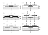
- FIG. 1 is a diagram showing a typical element configuration of a thin film transistor element using a metal oxide semiconductor according to the present invention.
- FIG. 4A to 4F are cross-sectional views showing some structural examples of thin film transistors.
- a source electrode 2 and a drain electrode 3 are configured so that a semiconductor layer 1 made of a metal oxide semiconductor is connected as a channel.
- FIG. 2A a source electrode 2 and a drain electrode 3 are formed on a support 6 by the method of the present invention, and this is used as a base material (substrate) to form a semiconductor layer 1 between both electrodes.
- a field effect thin film transistor is formed by forming an insulating layer 5 thereon and further forming a gate electrode 4 thereon.
- FIG. 6B shows the semiconductor layer 1 formed between the electrodes in FIG. 6A so as to cover the entire surface of the electrode and the support using a coating method or the like.
- (C) shows a structure in which the semiconductor layer 1 is first formed on the support 6, the source electrode 2, the drain electrode 3, and the insulating layer 5 are then formed, and then the gate electrode 4 is formed.
- the semiconductor layer may be formed by the method of the present invention.
- FIG. 4D after forming the gate electrode 4 on the support 6, the insulating layer 5 is formed, the source electrode 2 and the drain electrode 3 are formed thereon, and the semiconductor layer 1 is formed between the electrodes. To do.
- FIG. 2 is a schematic equivalent circuit diagram showing an example of a thin film transistor sheet in which a plurality of thin film transistor elements are arranged.
- the thin film transistor sheet 10 has a large number of thin film transistor elements 14 arranged in a matrix.
- Reference numeral 11 denotes a gate bus line of the gate electrode of each thin film transistor element 14, and reference numeral 12 denotes a source bus line of the source electrode of each thin film transistor element 14.
- An output element 16 is connected to the drain electrode of each thin film transistor element 14, and the output element 16 is, for example, a liquid crystal or an electrophoretic element, and constitutes a pixel in the display device.
- a liquid crystal is shown as an output element 16 by an equivalent circuit composed of a resistor and a capacitor.
- 15 is a storage capacitor
- 17 is a vertical drive circuit
- 18 is a horizontal drive circuit.
- the present invention can be used to manufacture the source, drain electrode and gate electrode of each transistor element in the thin film transistor sheet 10 as well as the gate bus line, source bus line and circuit wiring.
- the conductive material used for the electrodes such as the source electrode, the drain electrode, and the gate electrode constituting the TFT element is not particularly limited as long as it has conductivity at a practical level as an electrode.
- a conductive polymer or metal fine particles can be suitably used as the conductive material.
- a conductive polymer or metal fine particles for example, a known conductive paste may be used, but a dispersion containing metal fine particles having a particle diameter of 1 nm to 50 nm, preferably 1 nm to 10 nm is preferable.
- the above-described method can be used in the same manner, and the metal described above can be used as the material of the metal fine particles.
- Method for forming electrodes As a method for forming an electrode, a method for forming an electrode using a known photolithographic method or a lift-off method, using a conductive thin film formed by a method such as vapor deposition or sputtering using the above as a raw material, or a metal foil such as aluminum or copper There is a method in which a resist is formed and etched by thermal transfer, ink jet or the like. Alternatively, a conductive polymer solution or dispersion, a dispersion containing metal fine particles, or the like may be directly patterned by an ink jet method, or may be formed from a coating film by lithography or laser ablation. Further, a method of patterning a conductive ink or conductive paste containing a conductive polymer or metal fine particles by a printing method such as relief printing, intaglio printing, planographic printing, or screen printing can also be used.
- an electrode such as a source, drain, or gate electrode, a gate, or a source bus line without patterning a metal thin film using a photosensitive resin such as etching or lift-off
- a method by an electroless plating method there is a method by an electroless plating method.
- a liquid containing a plating catalyst that causes electroless plating by acting with a plating agent on a portion where an electrode is provided After patterning, for example, by a printing method (including inkjet printing), a plating agent is brought into contact with a portion where an electrode is provided. If it does so, electroless plating will be performed to the said part by the contact of the said catalyst and a plating agent, and an electrode pattern will be formed.
- the application of the electroless plating catalyst and the plating agent may be reversed, and the pattern formation may be performed either.
- a method of forming a plating catalyst pattern and applying the plating agent to this is preferable.
- the printing method for example, screen printing, planographic printing, letterpress printing, intaglio printing, printing by ink jet printing, or the like is used.
- Inorganic oxides include silicon oxide, aluminum oxide, tantalum oxide, titanium oxide, tin oxide, vanadium oxide, barium strontium titanate, barium zirconate titanate, lead zirconate titanate, lead lanthanum titanate, strontium titanate, Examples thereof include barium titanate, barium magnesium fluoride, bismuth titanate, strontium bismuth titanate, strontium bismuth tantalate, bismuth tantalate niobate, and yttrium trioxide. Of these, silicon oxide, aluminum oxide, tantalum oxide, and titanium oxide are preferable. Inorganic nitrides such as silicon nitride and aluminum nitride can also be suitably used.
- Examples of the method for forming the film include a vacuum process, a molecular beam epitaxial growth method, an ion cluster beam method, a low energy ion beam method, an ion plating method, a CVD method, a sputtering method, an atmospheric pressure plasma method, and a spray process.
- Examples include wet processes such as coating methods, spin coating methods, blade coating methods, dip coating methods, casting methods, roll coating methods, bar coating methods, die coating methods, and other methods such as printing and ink jet patterning. Can be used depending on the material.
- the wet process is a method of applying and drying a liquid in which fine particles of inorganic oxide are dispersed in an arbitrary organic solvent or water using a dispersion aid such as a surfactant as required, or an oxide precursor, for example,
- a so-called sol-gel method in which a solution of an alkoxide body is applied and dried is used.
- the atmospheric pressure plasma method described above is preferable.
- the gate insulating film is composed of an anodized film or the anodized film and an insulating film.
- the anodized film is preferably sealed.
- the anodized film is formed by anodizing a metal that can be anodized by a known method.
- Examples of the metal that can be anodized include aluminum and tantalum, and the anodizing method is not particularly limited, and a known method can be used.
- organic compound films examples include polyimides, polyamides, polyesters, polyacrylates, photo-radical polymerization-type, photo-cation polymerization-type photo-curing resins, copolymers containing acrylonitrile components, polyvinyl phenol, polyvinyl alcohol, novolac resins, etc. Can also be used.
- An inorganic oxide film and an organic oxide film can be laminated and used together.
- the thickness of these insulating films is generally 50 nm to 3 ⁇ m, preferably 100 nm to 1 ⁇ m.
- the support material constituting the substrate Various materials can be used as the support material constituting the substrate.
- ceramic substrates such as glass, quartz, aluminum oxide, sapphire, silicon nitride, silicon carbide, silicon, germanium, gallium arsenide, gallium phosphide.
- a semiconductor substrate such as gallium nitrogen, paper, and non-woven fabric can be used.
- the support is preferably made of a resin, for example, a plastic film sheet can be used.
- plastic films examples include polyethylene terephthalate (PET), polyethylene naphthalate (PEN), polyethersulfone (PES), polyetherimide, polyetheretherketone, polyphenylene sulfide, polyarylate, polyimide, polycarbonate (PC), and cellulose.
- PET polyethylene terephthalate
- PEN polyethylene naphthalate
- PES polyethersulfone
- CAP cellulose acetate propionate
- the weight can be reduced as compared with the case of using a glass substrate, the portability can be improved, and the resistance to impact can be improved.
- the protective layer includes the inorganic oxides and inorganic nitrides described above, and it is preferable to form the protective layer by the atmospheric pressure plasma method described above.
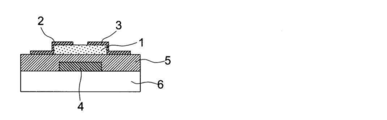
- Example FIG. 3 is a schematic cross-sectional view of the fabricated thin film transistor element.
- a glass substrate was used as the support 6, an aluminum film having a thickness of 300 nm was formed on the entire surface by sputtering, and then etched by photolithography to form the gate electrode 4.
- a gate insulating film 5 made of silicon oxide having a thickness of 200 nm was formed by atmospheric pressure plasma CVD.
- the atmospheric pressure plasma processing apparatus an apparatus according to FIG. 6 described in Japanese Patent Application Laid-Open No. 2003-303520 was used.
- a hollow rectangular stainless steel pipe was coated with the same dielectric as described above under the same conditions.
- the gate electrode 4 and the gate insulating layer (film) 5 were formed on the glass substrate as the support 6 (FIG. 3).
- the sputtering conditions are as follows.
- the substrate on which the semiconductor layer was formed was held in an electric furnace at a temperature of 200 ° C. for 30 minutes under reduced pressure (2.5 ⁇ 10 ⁇ 3 Pa), and post-baking was performed.
- the source electrode 2 and the drain electrode 3 were formed, and the thin film transistor element 101 was produced (FIG. 3).
- Each size was 10 ⁇ m wide, 50 ⁇ m long (channel width) and 50 nm thick, and the distance between the source electrode and the drain electrode (channel length) was 15 ⁇ m.
- a thin film transistor element 102 was manufactured in the same manner except that the post-baking process was replaced with the following microwave irradiation.
- Microwave irradiation was performed using microwave (2.45 GHz) under atmospheric pressure conditions using a multi-mode type 2.45 GHz microwave irradiator ( ⁇ -reactor manufactured by Shikoku Keiki Kogyo Co., Ltd.). Only the semiconductor surface side is kept warm with a heat insulating material, and microwave irradiation is performed for 15 minutes while adjusting the microwave output so that the surface temperature of the thin film becomes 200 ° C. using a thermocouple surface thermometer. Treated.
- a thin film transistor element 103 is similarly formed except that the gate electrode 4 is formed by an ITO film (thickness 150 nm) formed by sputtering and etching by photolithography, instead of the gate electrode made of aluminum. did.
- a gate insulating film 5 made of silicon oxide having a thickness of 200 nm was formed by the same atmospheric pressure plasma CVD method as described above.
- the gate electrode 4 and the gate insulating layer (film) 5 were formed on the glass substrate as the support 6 (FIG. 3).
- the metal oxide semiconductor precursor thin film turned transparent and converted to a metal oxide thin film, and the semiconductor layer 1 was formed (thickness 100 nm).
- a microwave (2.45 GHz) with an output of 500 W under atmospheric pressure conditions is applied to the substrate using a multi-mode type 2.45 GHz microwave irradiator ( ⁇ -reactor manufactured by Shikoku Keiki Kogyo Co., Ltd.). Irradiated. Only the semiconductor surface side was kept warm with a heat insulating material, and using a thermocouple surface thermometer, microwave irradiation was performed for 15 minutes while maintaining the surface temperature of the thin film at 200 ° C., and post-baking treatment was performed.
- the thin film transistor 104 was formed by forming the source electrode 2 and the drain electrode in the same manner as the thin film transistor element 101.
- a thin film transistor element 105 was formed in the same manner except that the semiconductor layer was formed by heat treatment (firing) by microwave irradiation (200 ° C., 15 minutes).
- the thin film transistor element 106 was formed in the same manner as the semiconductor precursor thin film except that indium nitrate, zinc nitrate, and gallium nitrate were used at a metal ratio of 1: 1: 0 (molar ratio).
- the semiconductor precursor thin film was formed by using an acetonitrile solution of a mixture of indium chloride, zinc chloride and gallium chloride (metal ratio 1: 1: 1 (molar ratio)) instead of nitrate.
- metal ratio 1: 1: 1 (molar ratio) metal ratio 1: 1: 1 (molar ratio)
- a polyimide film (thickness: 200 ⁇ m) was used as the support 6, and first, a corona discharge treatment was performed thereon under the condition of 50 W / m 2 / min. Thereafter, an undercoat layer was formed in order to improve adhesion as follows.
- a coating solution having the following composition was applied to a dry film thickness of 2 ⁇ m, dried at 90 ° C. for 5 minutes, and then cured for 4 seconds from a distance of 10 cm under a 60 W / cm high-pressure mercury lamp.
- Dipentaerythritol hexaacrylate monomer 60g Dipentaerythritol hexaacrylate dimer 20g Dipentaerythritol hexaacrylate trimer or higher component 20g Diethoxybenzophenone UV initiator 2g Silicone surfactant 1g 75g of methyl ethyl ketone Methyl propylene glycol 75g Further, a 50 nm thick silicon oxide film was provided on the layer by continuous atmospheric pressure plasma treatment under the following conditions, and these layers were used as the undercoat layer 8.
- a hollow rectangular stainless steel pipe was coated with the same dielectric as described above under the same conditions.
- a gate electrode is formed.
- An ITO film having a thickness of 150 nm was formed on one surface by sputtering, and then etched by photolithography to form a gate electrode 4 (FIG. 4 (2)).
- a silicon oxide film having a thickness of 150 nm was provided by the above-described atmospheric pressure plasma method at a film temperature of 200 ° C. to form a gate insulating layer (film) 5.
- a semiconductor layer was formed on the gate insulating layer in a portion serving as a channel region by the following method.
- An ink-jet coating was applied to the channel forming portion, and the semiconductor precursor thin film was formed by treatment at 150 ° C. for 10 minutes and drying.
- microwaves (2.45 GHz) were irradiated at an output of 500 W under atmospheric pressure conditions.
- the microwave irradiation only the semiconductor surface side was kept warm by a heat insulating material, and the surface temperature of the thin film was kept at 200 ° C. using a thermocouple surface thermometer, and the semiconductor layer 1 was formed by baking treatment for 15 minutes.
- the metal oxide semiconductor precursor thin film turned transparent and converted into a metal oxide thin film, and the semiconductor layer 1 was formed (thickness 100 nm).
- a post-bake treatment was performed in an electric furnace in an air atmosphere at a temperature of 200 ° C. for 30 minutes.
- Microwave irradiation was performed for 15 minutes while maintaining the surface temperature of the thin film at 200 ° C. under atmospheric pressure using the 2.45 GHz microwave irradiator ( ⁇ -reactor manufactured by Shikoku Keiki Kogyo Co., Ltd.).
- the thin film transistor elements exhibited n-type enhancement operation. For each element, an increase in drain current (transfer characteristic) was observed when the drain bias was 10 V and the gate bias was swept from ⁇ 10 V to +20 V.
- the mobility (cm 2 / Vs) estimated from the saturation region, the on / off ratio (log value (number of digits)), and the threshold value (Vth) were evaluated.
- Each of the fabricated thin film transistor elements exhibited an n-type enhancement operation, but the variation in characteristics of the semiconductor layer sputter-deposited by microwave post-baking was reduced, and the effect was generated by ITO generated by the microwave in the gate electrode. It can be seen that when using is larger.
- a semiconductor precursor formed by coating, a semiconductor formed by subsequent baking treatment, and subjected to a post-baking treatment by microwaves has particularly high mobility, a small threshold value, and a very small variation in characteristics. I understand that.
- a semiconductor precursor formed by coating, a semiconductor formed by microwave heating, and post-baked by microwave was particularly good.
- the thin film transistor element 108 post-baked in an electric furnace
- the thin film transistor element 108 not only the element characteristics are worse than the element of the present invention, but also deformation of the substrate (occurrence of curling and deflection) occurs. It became difficult to use practically.
Landscapes
- Thin Film Transistor (AREA)
- Liquid Deposition Of Substances Of Which Semiconductor Devices Are Composed (AREA)
Abstract
本発明は、高いプロセス温度を必要とせず、安定した優れた半導体性能を有する金属酸化物半導体の製造方法を提供することにあり、また、生産性の高い製造方法を提供する。
本発明の製造方法は、金属酸化物半導体形成後に、マイクロ波を照射して後加熱を行うことを特徴とする。
Description
本発明は、金属酸化物半導体形成後に後加熱を行う金属酸化物半導体の製造方法、およびこれを用いる半導体素子に関するものである。
金属酸化物半導体について、また、これを用いた薄膜トランジスタ(TFT)素子についてはよく知られている。金属酸化物半導体は、スパッタ法により形成したり、また、例えば基板上に形成した金属膜や、金属の塩、また有機金属等を、熱酸化やプラズマ酸化等により分解酸化して金属酸化物半導体に変換する方法も知られている。
しかしながら、このような金属酸化物半導体については単に成膜したのみでは充分な性能が出ないことも多く、例えば、非特許文献1また2で示されているようなスパッタ成膜法(室温)によって得られる半導体膜についても、成膜直後は性能が出ない、または性能ばらつきが大きいなど、性能安定化のためには300℃以上で30分程度のポストベークが必要であることが報告されている。
そのため、室温程度で成膜は可能であっても、製品レベルの安定した性能を得るためには300℃以上の高温に晒されるため、実質的に樹脂基板への応用が難しい。
非特許文献3また4では、金属塩化物前駆体から600℃の処理で金属酸化物半導体としての性能を引き出しているが、高温長時間の熱処理によっても実際にそれだけでは求める性能が出ない場合が多い。
また、高温長時間の熱処理の必要性は、樹脂基板への応用を難しくしている。
薄膜材料デバイス研究会第4回研究集会予稿集P-29(194頁-195頁) 薄膜材料デバイス研究会第4回研究集会予稿集P-30(196頁-197頁) Electrochemical and Solid-State Letters 10(5)H135-H138(2007) Advanced Materals 2007、19,183-187
薄膜材料デバイス研究会第4回研究集会予稿集P-29(194頁-195頁) 薄膜材料デバイス研究会第4回研究集会予稿集P-30(196頁-197頁) Electrochemical and Solid-State Letters 10(5)H135-H138(2007) Advanced Materals 2007、19,183-187
従って本発明の目的は、金属酸化物半導体の作製において、後加熱(ポストベーク)にマイクロ波使用することで、高いプロセス温度を必要とせず、安定した、優れた半導体性能を有する金属酸化物半導体の製造方法を提供することにあり、また、生産性の高い製造方法を提供することにある。
本発明の上記課題は以下の手段により達成される。
1.金属酸化物半導体形成後に、マイクロ波を照射して後加熱を行うことを特徴とする金属酸化物半導体の製造方法。
2.金属酸化物半導体が少なくともIn、Zn、Snのいずれかを含むことを特徴とする前記1に記載の金属酸化物半導体の製造方法。
3.金属酸化物半導体が少なくともGa、Alのいずれかを含むことを特徴とする前記1または2に記載の金属酸化物半導体の製造方法。
4.近接または隣接する電極の少なくとも1つの電極にIn、Zn、Snのいずれか1つ以上が含まれることを特徴とする前記1~3のいずれか1項に記載の金属酸化物半導体の製造方法。
5.金属酸化物半導体が半導体前駆体を塗布後、半導体変換処理を行うことで形成されることを特徴とする前記1~4のいずれか1項に記載の金属酸化物半導体の製造方法。
6.半導体変換処理がマイクロ波(周波数0.3GHz~50GHz)照射であることを特徴とする前記5に記載の金属酸化物半導体の製造方法。
7.半導体前駆体が金属塩であることを特徴とする前記5または6に記載の金属酸化物半導体の製造方法。
8.前記1~7のいずれか1項に記載の金属酸化物半導体の製造方法で製造された金属酸化物半導体を用いることを特徴とする半導体素子。
金属酸化物半導体層の作製において、ポストベークにマイクロ波使用することで、高いプロセス温度を必要とせず、金属酸化物半導体の形成が可能となる。また、金属酸化物半導体層または前駆体薄膜の成膜自体はスパッタおよび塗布でも可能であるが、金属酸化物半導体前駆体薄膜を塗布で形成する場合においては、焼成およびポストベークともマイクロ波使用することで、実質高いプロセス温度が必要なく金属酸化物半導体の形成が可能となる。特に、塗布の場合、硝酸塩前駆体の選択により、より低温で、処理時間の短縮も可能となる。
1 半導体層
2 ソース電極
3 ドレイン電極
4 ゲート電極
5 ゲート絶縁層
6 支持体
10 薄膜トランジスタシート
11 ゲートバスライン
12 ソースバスライン
14 薄膜トランジスタ素子
15 蓄積コンデンサ
16 出力素子
17 垂直駆動回路
18 水平駆動回路
2 ソース電極
3 ドレイン電極
4 ゲート電極
5 ゲート絶縁層
6 支持体
10 薄膜トランジスタシート
11 ゲートバスライン
12 ソースバスライン
14 薄膜トランジスタ素子
15 蓄積コンデンサ
16 出力素子
17 垂直駆動回路
18 水平駆動回路
以下本発明を実施するための最良の形態について説明するが本発明はこれにより限定されるものではない。
本発明は、金属酸化物半導体形成後に、マイクロ波を照射して後加熱(ポストベーク)を行うことで、金属酸化物半導体のキャリア移動度、またTFT素子としたときのon/off値などの性能向上を達成した金属酸化物半導体の製造方法に関するものである。
金属酸化物半導体としては、下記の金属原子を含む金属酸化物からなるものを挙げることができる。
金属として、Li、Be、B、Na、Mg、Al、Si、K、Ca、Sc、Ti、V、Cr、Mn、Fe、Co、Ni、Cu、Zn、Ga、Ge、Rb、Sr、Y、Zr、Nb、Mo、Cd、In、Ir、Sn、Sb、Cs、Ba、La、Hf、Ta、W、Tl、Pb、Bi、Ce、Pr、Nd、Pm、Eu、Gd、Tb、Dy、Ho、Er、Tm、Yb、Lu等を含む金属酸化物からなるものを挙げることができる。
本発明の方法により、前述した金属原子から選ばれた単独、または複数の金属原子を含む金属酸化物半導体の薄膜を作製する。金属酸化物半導体としては、単結晶、多結晶、非晶質のいずれの状態も使用可能だが、好ましくは非晶質の薄膜を用いる。
それらのうち、金属酸化物半導体としては、インジウム、錫、亜鉛のいずれかの金属を含むことが好ましく、それらを併用して混合させてもよい。また、その他の金属として、ガリウムまたはアルミニウムを含むことが好ましい。
好ましい金属の組成比としては、In、Snの金属塩から選ばれる塩に含有される金属(金属A)と、Ga、Alの金属塩から選ばれる塩に含有される金属(金属B)と、Znの金属塩に含有される金属(金属C=Zn)とのモル比率(金属A:金属B:金属C)が、以下の関係式を満たすことが好ましい。
金属A:金属B:金属C=1:0~2:0~5
である。また、比較的低温での半導体変換処理では金属Cの比率が上式で0~2になることが、より好ましい。明確な理由は定かではないが、金属Cを含む前駆体材料の酸化反応温度が比較的高いためと推定している。
である。また、比較的低温での半導体変換処理では金属Cの比率が上式で0~2になることが、より好ましい。明確な理由は定かではないが、金属Cを含む前駆体材料の酸化反応温度が比較的高いためと推定している。
本発明に係る前記の金属酸化物半導体の電子キャリア濃度は、1018/cm3未満である。このキャリア濃度は、室温で測定する場合の値である。室温とは、例えば25℃であり、具体的には0℃から40℃程度の範囲から適宜選択されるある温度である。なお、本発明に係るアモルファス酸化物の電子キャリア濃度は、0℃から40℃の範囲全てにおいて、1018/cm3未満を充足する必要はない。例えば、25℃において、キャリア電子密度1018/cm3未満が実現されていればよい。また、電子キャリア濃度をさらに下げ、1017/cm3以下、より好ましくは1016/cm3以下にするとノーマリーオフのTFTが歩留まり良く得られる。
電子キャリア濃度の測定は、ホール効果測定により求めることができる。
金属酸化物である半導体の膜厚としては、特に制限はないが、得られたトランジスタの特性は、半導体膜の膜厚に大きく左右される場合が多く、その膜厚は、半導体により異なるが、一般に1μm以下、特に1~300nmが好ましく、より好ましくは、5~200nm、さらに好ましくは10~100nmである。
本発明においては、金属酸化物半導体の前駆体材料またターゲット等の組成、また製造(成膜)条件などを制御して、例えば、電子キャリア濃度を、1012/cm3以上1018/cm3未満とする。より好ましくは1013/cm3以上1017/cm3以下、さらには1015/cm3以上1016/cm3以下の範囲にすることが好ましい。
これらの金属酸化物半導体は、例えば、前記非特許文献1また2に記載されたように、スパッタ法により、成膜時の雰囲気を精密に制御することにより、室温程度の温度で金属酸化物半導体膜を基材上に堆積させることが可能である。しかし、実際には、これのみでは充分な性能が発現しないことが多く、また、性能のバラつきが大きいため安定化のための後処理として、電気炉による300℃以上の熱処理(ポストベーク)を施して安定化させている。ポストベーク処理はキャリア密度やバンドの最適化を何らかの作用によって行っていると考えられるが、その作用機作は明確ではない。本発明は、これら一旦形成された金属酸化物半導体膜にポストベーク処理として、マイクロ波照射を行うことを特徴とするものである。但し、金属酸化物半導体の製造方法について特に限定されない。
本発明においてはポストベーク処理として、マイクロ波照射を行えば300℃以上の高温による長時間での熱処理を必要とせず、低温化、また処理時間の短縮も可能であることが判った。また、樹脂基板を用いると従来のポストベーク処理においては、300℃以上の高温が必要であるため、基板の変形、変質が起こり、適用が難しかったが、マイクロ波照射によれば基板へのダメージがなく実施できる。
(マイクロ波の照射)
本発明においては、ポストベーク処理としてマイクロ波(0.3GHz~50GHz)照射を用いる。本発明においては、金属酸化物半導体、またその前駆体となる金属酸化物薄膜を形成した後、該薄膜に対し、電磁波、特にマイクロ波(周波数0.3GHz~50GHz)を照射してポストベーク処理を行う。
本発明においては、ポストベーク処理としてマイクロ波(0.3GHz~50GHz)照射を用いる。本発明においては、金属酸化物半導体、またその前駆体となる金属酸化物薄膜を形成した後、該薄膜に対し、電磁波、特にマイクロ波(周波数0.3GHz~50GHz)を照射してポストベーク処理を行う。
本発明におけるポストベーク温度は、300℃以下が好ましく、耐熱性の低い機樹脂基板に適用する観点からは250℃以下がより好ましい。300℃より高い温度を用いても安定化の効果は既に飽和領域なため、安定化のためのエネルギー効率を損なう事になる。
金属酸化物半導体薄膜にマイクロ波を照射することで、金属酸化物中の電子が振動し、ジュール熱が発生して薄膜が内部から、均一に加熱される。ガラスや樹脂等の基板には、マイクロ波領域に吸収が殆どないため、半導体の基板自体は殆ど発熱せずに半導体薄膜部のみを選択的に加熱することが可能となる。
マイクロ波加熱においては、マイクロ波吸収は吸収が強い物質に集中し、尚且つ非常に短時間で500~600℃にまで昇温することが可能なため、本発明にこの方法を用いた場合に、基板自身には電磁波による加熱の影響を与えず、短時間で薄膜のみを焼成、またポストベーク温度まで昇温することが可能となる。金属酸化物半導体材料、また基板材料によっても変わるが、ポストベークにおける加熱温度、加熱時間は照射するマイクロ波の出力、照射時間で制御することが可能であり、任意の温度と時間を選択可能であるが、好ましくは300℃以下、耐熱性の低い樹脂基板を使用する観点から、より好ましくは250℃以下の温度に、薄膜表面がなるよう調整する。薄膜表面の温度、基板の温度等は熱電対を用いた表面温度計、また非接触の表面温度計により測定が可能である。また、前駆体材料を加熱する時間は、任意に設定できるが、電子デバイスの特性や生産効率の観点から、1秒以上60分以下の範囲が好ましい。より好ましくは5分~30分である。
一般的に、マイクロ波とは0.3GHz~50GHzの周波数を持つ電磁波のことを指し、携帯通信で用いられる0.8MHzおよび1.5GHz帯、2GHz帯、アマチュア無線、航空機レーダー等で用いられる1.2GHz帯、電子レンジ、構内無線、VICS等で用いられる2.4GHz帯、船舶レーダー等に用いられる3GHz帯、その他ETCの通信に用いられる5.6GHzなどは全てマイクロ波の範疇に入る電磁波である。
また、本発明においては、近接または隣接する電極の少なくとも1つの電極にIn、Zn、Snのいずれか1つ以上が含まれることが好ましい。半導体デバイス、TFT素子等においては、半導体層に接してあるいは隣接してソース、ドレイン電極、またゲート電極、バスライン等を備えているが、これらのいずれかあるいは全てでもよいが、これらに、例えば、導電体であるITO等を用いると、In酸化物、Zn酸化物、そして特にSn酸化物は特に電磁波吸収能が高いので、電極パターン部も発熱し熱源となるので、この上の、半導体薄膜の電極パターン部とその近傍を同時に加熱でき、ポストベークの効率を上げることができる。
オーブンなどを用いた通常の加熱方法に比較し、本発明の電磁波(マイクロ波)照射による加熱方法を用いることで、より良好な金属酸化物半導体層を得ることができる。金属酸化物半導体前駆体材料から金属酸化物半導体が生成するに際し、伝導熱以外の作用、例えば金属酸化物半導体前駆体材料への電磁波の直接的な作用を示唆する効果が得られている。機構は十分に明らかになっていないが、金属酸化物半導体前駆体材料の加水分解や脱水、分解、酸化等による金属酸化物半導体への転化が電磁波により促進された結果と推定される。
(前駆体を用いる金属酸化物半導体)
金属酸化物半導体は、前記非特許文献1また2にも記載されたようにスパッタ法等により形成されるほか、金属酸化物半導体の前駆体となる金属酸化物の金属成分を含む薄膜を設け、酸素の存在下で該薄膜に半導体変換処理を行って、金属酸化物半導体に変換する方法で形成することもできる。本発明においては、前駆体に、半導体変換処理を行って金属酸化物半導体を形成することが好ましい。半導体変換処理としては、熱酸化やプラズマ酸化等があり、本発明においては、電磁波(マイクロ波)を照射する半導体変換処理を含むことが好ましい。また、酸素の存在下で、マイクロ波を照射することが、短時間で金属酸化物半導体前駆体の酸化反応を進行させる上で好ましい。半導体変換処理後、やはり条件をかえてマイクロ波照射することでポストベーク処理を行って金属酸化物半導体の性能向上を達成することができる。
金属酸化物半導体は、前記非特許文献1また2にも記載されたようにスパッタ法等により形成されるほか、金属酸化物半導体の前駆体となる金属酸化物の金属成分を含む薄膜を設け、酸素の存在下で該薄膜に半導体変換処理を行って、金属酸化物半導体に変換する方法で形成することもできる。本発明においては、前駆体に、半導体変換処理を行って金属酸化物半導体を形成することが好ましい。半導体変換処理としては、熱酸化やプラズマ酸化等があり、本発明においては、電磁波(マイクロ波)を照射する半導体変換処理を含むことが好ましい。また、酸素の存在下で、マイクロ波を照射することが、短時間で金属酸化物半導体前駆体の酸化反応を進行させる上で好ましい。半導体変換処理後、やはり条件をかえてマイクロ波照射することでポストベーク処理を行って金属酸化物半導体の性能向上を達成することができる。
金属酸化物半導体の前駆体としての金属原子含有化合物には、金属原子を含む、金属塩、ハロゲン化物、金属酸化物、有機金属化合物、金属水素化合物等を挙げることができる。
金属塩、有機金属化合物、ハロゲン化物、金属水素化合物中の金属としては、前記金属酸化物半導体において挙げられた金属を同様に挙げることができる。また、それらの金属原子含有化合物は、インジウム、錫、亜鉛のいずれかを含むことが好ましく、それらを併用して混合させてもよい。また、その他の金属として、ガリウムまたはアルミニウムを含むことが好ましい。それらを併用して混合させてもよい。
金属塩としては、硝酸塩、硫酸塩、燐酸塩、酢酸塩、蓚酸塩等を、またハロゲン化物としては塩化物、ヨウ化物、臭化物等を好適に用いることができる。
有機金属化合物としては、下記の一般式(I)で示すものが挙げられる。
一般式(I) R1
xMR2
yR3
z
式中、Mは金属、R1はアルキル基、R2はアルコキシ基、R3はβ-ジケトン錯体基、β-ケトカルボン酸エステル錯体基、β-ケトカルボン酸錯体基およびケトオキシ基(ケトオキシ錯体基)から選ばれる基であり、金属Mの価数をmとした場合、x+y+z=mであり、x=0~m、またはx=0~m-1であり、y=0~m、z=0~mで、いずれも0または正の整数である。R1のアルキル基としては、メチル基、エチル基、プロピル基、ブチル基等を挙げることができる。R2のアルコキシ基としては、メトキシ基、エトキシ基、プロポキシ基、ブトキシ基、3,3,3-トリフルオロプロポキシ基等を挙げることができる。またアルキル基の水素原子をフッ素原子に置換したものでもよい。R3のβ-ジケトン錯体基、β-ケトカルボン酸エステル錯体基、β-ケトカルボン酸錯体基およびケトオキシ基(ケトオキシ錯体基)から選ばれる基としては、β-ジケトン錯体基として、例えば、2,4-ペンタンジオン(アセチルアセトンあるいはアセトアセトンともいう)、1,1,1,5,5,5-ヘキサメチル-2,4-ペンタンジオン、2,2,6,6-テトラメチル-3,5-ヘプタンジオン、1,1,1-トリフルオロ-2,4-ペンタンジオン等を挙げることができ、β-ケトカルボン酸エステル錯体基として、例えばアセト酢酸メチルエステル、アセト酢酸エチルエステル、アセト酢酸プロピルエステル、トリメチルアセト酢酸エチル、トリフルオロアセト酢酸メチル等を挙げることができ、β-ケトカルボン酸として、例えば、アセト酢酸、トリメチルアセト酢酸等を挙げることができ、またケトオキシとして、例えば、アセトオキシ基(またはアセトキシ基)、プロピオニルオキシ基、ブチリロキシ基、アクリロイルオキシ基、メタクリロイルオキシ基等を挙げることができる。これらの基の炭素原子数は18以下が好ましい。また直鎖または分岐のもの、また水素原子をフッ素原子にしたものでもよい。有機金属化合物のなかでは、分子内に少なくとも1つ以上の酸素を有するものが好ましい。このようなものとしてR2のアルコキシ基を少なくとも1つを含有する有機金属化合物、またR3のβ-ジケトン錯体基、β-ケトカルボン酸エステル錯体基、β-ケトカルボン酸錯体基およびケトオキシ基(ケトオキシ錯体基)から選ばれる基を少なくとも1つ有する金属化合物が最も好ましい。金属塩のなかでは、硝酸塩が好ましい。硝酸塩は高純度品が入手しやすく、また使用時の媒体として好ましい水に対する溶解度が高い。硝酸塩としては、硝酸インジウム、硝酸錫、硝酸亜鉛、硝酸ガリウム等が挙げられる。
式中、Mは金属、R1はアルキル基、R2はアルコキシ基、R3はβ-ジケトン錯体基、β-ケトカルボン酸エステル錯体基、β-ケトカルボン酸錯体基およびケトオキシ基(ケトオキシ錯体基)から選ばれる基であり、金属Mの価数をmとした場合、x+y+z=mであり、x=0~m、またはx=0~m-1であり、y=0~m、z=0~mで、いずれも0または正の整数である。R1のアルキル基としては、メチル基、エチル基、プロピル基、ブチル基等を挙げることができる。R2のアルコキシ基としては、メトキシ基、エトキシ基、プロポキシ基、ブトキシ基、3,3,3-トリフルオロプロポキシ基等を挙げることができる。またアルキル基の水素原子をフッ素原子に置換したものでもよい。R3のβ-ジケトン錯体基、β-ケトカルボン酸エステル錯体基、β-ケトカルボン酸錯体基およびケトオキシ基(ケトオキシ錯体基)から選ばれる基としては、β-ジケトン錯体基として、例えば、2,4-ペンタンジオン(アセチルアセトンあるいはアセトアセトンともいう)、1,1,1,5,5,5-ヘキサメチル-2,4-ペンタンジオン、2,2,6,6-テトラメチル-3,5-ヘプタンジオン、1,1,1-トリフルオロ-2,4-ペンタンジオン等を挙げることができ、β-ケトカルボン酸エステル錯体基として、例えばアセト酢酸メチルエステル、アセト酢酸エチルエステル、アセト酢酸プロピルエステル、トリメチルアセト酢酸エチル、トリフルオロアセト酢酸メチル等を挙げることができ、β-ケトカルボン酸として、例えば、アセト酢酸、トリメチルアセト酢酸等を挙げることができ、またケトオキシとして、例えば、アセトオキシ基(またはアセトキシ基)、プロピオニルオキシ基、ブチリロキシ基、アクリロイルオキシ基、メタクリロイルオキシ基等を挙げることができる。これらの基の炭素原子数は18以下が好ましい。また直鎖または分岐のもの、また水素原子をフッ素原子にしたものでもよい。有機金属化合物のなかでは、分子内に少なくとも1つ以上の酸素を有するものが好ましい。このようなものとしてR2のアルコキシ基を少なくとも1つを含有する有機金属化合物、またR3のβ-ジケトン錯体基、β-ケトカルボン酸エステル錯体基、β-ケトカルボン酸錯体基およびケトオキシ基(ケトオキシ錯体基)から選ばれる基を少なくとも1つ有する金属化合物が最も好ましい。金属塩のなかでは、硝酸塩が好ましい。硝酸塩は高純度品が入手しやすく、また使用時の媒体として好ましい水に対する溶解度が高い。硝酸塩としては、硝酸インジウム、硝酸錫、硝酸亜鉛、硝酸ガリウム等が挙げられる。
以上の前駆体のうち、好ましいのは、金属の硝酸塩、硫酸塩、燐酸塩、酢酸塩、蓚酸塩等、ハロゲン化物、アルコキシド類である。具体例としては、硝酸インジウム、硝酸亜鉛、硝酸ガリウム、硝酸スズ、硝酸アルミニウム、硫酸インジウム、硫酸亜鉛、硫酸ガリウム、塩化インジウム、塩化亜鉛、塩化スズ(2価)、塩化スズ(4価)、塩化ガリウム、塩化アルミニウム、トリ-i-プロポキシインジウム、ジエトキシ亜鉛、ビス(ジピバロイルメタナト)亜鉛、テトラエトキシスズ、テトラ-i-プロポキシスズ、トリ-i-プロポキシガリウム、トリ-i-プロポキシアルミニウムなどが挙げられる。
特に、前記硝酸塩、硫酸塩、燐酸塩、炭酸塩、酢酸塩または蓚酸塩から選ばれる金属塩は、他の金属塩、ハロゲン化物、アルコキシド類また有機金属化合物を用いる場合に比べ半導体特性が優れ好ましい。また、水を溶媒として用いることができる点、製造上、環境上も好ましい。酸化物生成過程で発生する分解物が効率よく気化、排出されるために膜に残存しにくく、生成した酸化物中に存在する炭素などの不純物成分が少ないため、良好な半導体特性が得られるものと推定される。不純物低減、半導体特性の向上の観点から、上記金属塩の中でも硝酸塩が最も好ましい。
これらの塩を用いると、また、半導体変換処理として電磁波(マイクロ波)で実質低温において変換するとき照射時間を短くでき有利になる。
(前駆体薄膜の成膜方法、パターン化方法)
これらの金属酸化物半導体の前駆体となる金属を含有する薄膜を形成するためには、公知の成膜法、真空蒸着法、分子線エピタキシャル成長法、イオンクラスタービーム法、低エネルギーイオンビーム法、イオンプレーティング法、CVD法、スパッタリング法、大気圧プラズマ法などを用いることができるが、本発明については金属塩、ハロゲン化物、有機金属化合物等を適切な溶媒に溶解した溶液を用いて基板上に連続的に塗設することで生産性を大幅に向上することができる。金属化合物としては、塩化物、硝酸塩、酢酸塩、金属アルコキシド等を用いることが溶解性の観点からより好ましい。
これらの金属酸化物半導体の前駆体となる金属を含有する薄膜を形成するためには、公知の成膜法、真空蒸着法、分子線エピタキシャル成長法、イオンクラスタービーム法、低エネルギーイオンビーム法、イオンプレーティング法、CVD法、スパッタリング法、大気圧プラズマ法などを用いることができるが、本発明については金属塩、ハロゲン化物、有機金属化合物等を適切な溶媒に溶解した溶液を用いて基板上に連続的に塗設することで生産性を大幅に向上することができる。金属化合物としては、塩化物、硝酸塩、酢酸塩、金属アルコキシド等を用いることが溶解性の観点からより好ましい。
溶媒としては、水のほか、用いる金属化合物を溶解するものであれば特に制限されるところではないが、水や、エタノール、プロパノール、エチレングリコールなどのアルコール類、テトラヒドロフラン、ジオキサン等のエーテル系、酢酸メチル、酢酸エチル等のエステル系、アセトン、メチルエチルケトン、シクロヘキサノン等のケトン系、ジエチレングリコールモノメチルエーテル等グリコールエーテル系、また、アセトニトリルなど、さらに、キシレン、トルエン等の芳香族炭化水素系溶媒、o-ジクロロベンゼン、ニトロベンゼン、m-クレゾール等の芳香族系溶媒、ヘキサン、シクロヘキサン、トリデカンなどの脂肪族炭化水素溶媒、α-テルピネオール、また、クロロホルムや1,2-ジクロロエタン等のハロゲン化アルキル系溶媒、N-メチルピロリドン、2硫化炭素等を好適に用いることができる。
金属原子含有化合物を溶解する溶媒は、金属塩等、金属原子含有化合物が溶解する溶媒であれば特に限定されないが、金属塩等の溶解性、塗布後の乾燥性の観点から水および低級アルコールが好ましく、低級アルコールの中ではメタノール、エタノール、プロパノール(1-プロパノールおよびイソプロパノール)が乾燥性の観点で好ましい。また、溶媒としてアルコールを単独で用いても良いし、水と任意の割合で混合して用いても良い。溶解性と溶液安定性および乾燥性の観点から水とこれらの低級アルコール類を混合して水溶液を作成することが好ましい。
本発明において水溶液とは溶媒中の水含有率が30質量%以上の混合溶媒および水(含有率=100質量%)に溶質(本発明では金属塩等、金属原子含有化合物とその他必要に応じて添加剤)を溶解した溶液を意味する。金属塩等溶質の溶解性、溶液安定性の観点から好ましくは水含有率は50質量%以上であり、さらに好ましくは水含有率が70質量%以上である。
また、溶媒中に金属アルコキシドと種々のアルカノールアミン、α-ヒドロキシケトン、β-ジケトンなどの多座配位子であるキレート配位子を添加すると、金属アルコキシドを安定化したり、カルボン酸塩の溶解度を増加させることができるので、悪影響が出ない範囲で添加することが好ましい。
また、前記硝酸塩、硫酸塩、燐酸塩、炭酸塩、酢酸塩または蓚酸塩から選ばれる金属塩を用いると金属アルコキシド類のように室温で加水分解することがなく、水を主たる溶媒として用いることができ、前記のように好ましい。
本発明において、薄膜形成材料を含有する液体を基材上に適用して、金属酸化物半導体の前駆体を含有する薄膜を形成する方法としては、スプレーコート法、スピンコート法、ブレードコート法、ディップコート法、キャスト法、ロールコート法、バーコート法、ダイコート法、ミスト法、など、凸版、凹版、平版、スクリーン印刷、インクジェットなどの印刷法等、広い意味での塗布による方法が挙げられ、また、これによりパターン化する方法などが挙げられる。塗布膜からフォトリソグラフ法、レーザーアブレーションなどによりパターン化してもよい。これらのうち、好ましいのは薄膜の塗布が可能な、インクジェット法、スプレーコート法等である。
塗布プロセス(印刷やインクジェット法)が可能になることで、大気圧下での成膜が可能になり、さらには低温での製造が可能な、生産効率の高い、半導体変換処理を行って、金属酸化物半導体層を製造する方法を提供することが可能となる。
例えばインクジェット法を用いて成膜する場合、金属化合物溶液を滴下して、150℃程度で溶媒を揮発させることにより金属酸化物の前駆体の薄膜が形成される。尚、溶液を滴下する際、基板自体を150℃程度に加熱しておくと、塗布、乾燥の二つのプロセスを同時に行えるため好ましい。また、ポストベーク処理もマイクロ波照射条件を変更して行う(穏和な条件で)ことで、連続して焼成、ポストベーク処理を行うこともできる。
こうして得られる金属酸化物半導体の、好ましい金属の組成比としては、In、Snの金属塩から選ばれる塩に含有される金属(金属A)と、Ga、Alの金属塩から選ばれる塩に含有される金属(金属B)と、Znの金属塩に含有される金属(金属C=Zn)とのモル比率(金属A:金属B:金属C)が、以下の関係式を満たすことが好ましい。
金属A:金属B:金属C=1:0~2:0~5
である。
である。
前駆体薄膜の膜厚は1~300nm、より好ましくは5~200nmである。
(非晶質酸化物)
これらの金属酸化物半導体の前駆体膜に半導体変換処理を行って金属酸化物半導体は形成されるが、半導体としては、単結晶、多結晶、非晶質のいずれの状態も使用可能だが、好ましくは非晶質の薄膜を用いる。
これらの金属酸化物半導体の前駆体膜に半導体変換処理を行って金属酸化物半導体は形成されるが、半導体としては、単結晶、多結晶、非晶質のいずれの状態も使用可能だが、好ましくは非晶質の薄膜を用いる。
金属酸化物半導体の前駆体となる金属化合物材料から形成された、本発明に係る金属酸化物である非晶質酸化物の電子キャリア濃度は、前記のように、1018/cm3未満が実現されていればよく、前駆体材料(金属塩)、組成比、製造条件、また、半導体変換処理条件などを制御して、例えば、電子キャリア濃度を、1012/cm3以上1018/cm3未満とする。より好ましくは1013/cm3以上1017/cm3以下、さらには1015/cm3以上1016/cm3以下の範囲にすることが好ましいものである。
電子キャリア濃度の測定は、ホール効果測定により求めることができる。
(半導体変換処理)
前駆体膜を半導体に変換する前記半導体変換処理としては、熱酸化法、酸素プラズマ法、UVオゾン法等の酸化処理、また、酸素存在下でのマイクロ波照射が挙げられる。
前駆体膜を半導体に変換する前記半導体変換処理としては、熱酸化法、酸素プラズマ法、UVオゾン法等の酸化処理、また、酸素存在下でのマイクロ波照射が挙げられる。
熱酸化としては、100℃以上400℃以下の温度域で酸素の存在下加熱処理することが好ましい。本発明の硝酸塩、硫酸塩、燐酸塩、炭酸塩、酢酸塩または蓚酸塩から選ばれる金属塩を用いることで比較的低い温度において半導体変換処理を行うことができる。
また、金属酸化物の形成はESCA等により検知でき、半導体への変換が充分行われる条件を予め選択することができる。
また、酸素プラズマ法としては大気圧プラズマ法を用いるのが好ましい。また酸素プラズマ法、UVオゾン法においては、基板を50℃~300℃の範囲で加熱させることが好ましい。
大気圧プラズマ法では、大気圧下で、アルゴンガス等の不活性ガスを放電ガスとして、これと共に反応ガス(酸素を含むガス)を放電空間に導入して、高周波電界を印加して、放電ガスを励起させ、プラズマ発生させ、反応ガスと接触させて酸素を含むプラズマを発生させ、基体表面をこれに晒すことで酸素プラズマ処理を行う。大気圧下とは、20~110kPaの圧力を表すが、好ましくは93~104kPaである。
大気圧プラズマ法を用いて、酸素含むガスを反応性ガスとして、酸素プラズマを発生させ、前駆体薄膜を、プラズマ空間に晒すことでプラズマ酸化により前駆体薄膜は酸化分解して、金属酸化物からなる薄膜が形成する。
高周波電源として0.5kHz以上、2.45GHz以下、また、対向電極間に供給する電力は、好ましくは0.1W/cm2以上、50W/cm2以下である。
使用するガスは、基本的に、放電ガス(不活性ガス)と、反応ガス(酸化性ガス)の混合ガスである。反応ガスは好ましくは酸素ガスであり混合ガスに対し、0.01~10体積%含有させることが好ましい。0.1~10体積%であることがより好ましいが、さらに好ましくは、0.1~5体積%である。
上記不活性ガスとしては、周期表の第18属元素、具体的には、ヘリウム、ネオン、アルゴン、クリプトン、キセノン、ラドンや、窒素ガス等が挙げられるが、本発明に記載の効果を得るためには、ヘリウム、アルゴン、窒素ガスが好ましく用いられる。
また、反応ガスを放電空間である電極間に導入するには、常温常圧で構わない。
大気圧下でのプラズマ法については特開平11-61406号、同11-133205号、特開2000-121804号、同2000-147209号、同2000-185362号等に記載されている。
また、UVオゾン法は、酸素の存在下で、紫外光を照射し、酸化反応を進行させる方法である。紫外光の波長は、100nm~450nm、特に好ましくは150~300nm程度の所謂、真空紫外光を照射することが好ましい。光源は、低圧水銀灯、重水素ランプ、キセノンエキシマーランプ、メタルハライドランプ、エキシマーレーザーなどを用いることができる。
ランプの出力としては400W~30kW、照度としては100mW/cm2~100kW/cm2、照射エネルギーとしては10~5000mJ/cm2が好ましく、100~2000mJ/cm2がより好ましい。
紫外線照射の際の照度は1mW~10W/cm2が好ましい。
また、本発明においては、酸化処理に加えて前記酸化処理の後、あるいは前記酸化処理と同時に加熱処理を施すことが好ましい。これにより酸化分解を促進できる。
また、前駆体材料を加熱する時間は、任意に設定できるが、電子デバイスの特性や生産効率の観点から、1秒以上60分以下の範囲が好ましい。より好ましくは5分~30分である。
加熱処理は、酸化処理と同時に行ってもよく、酸化による金属酸化物半導体への変換を迅速に行うことができる。
金属酸化物半導体への変換後、形成される半導体薄膜の膜厚は、1~300nmが好ましく、より好ましくは、5~200nm、さらに好ましくは5~100nmである。
前記半導体変換処理として、本発明においては、前記マイクロ波(0.3GHz~50GHz)照射を用いることが好ましい。また、酸素の存在下で、マイクロ波を照射することが、短時間で金属酸化物半導体前駆体の酸化反応を進行させる上で好ましい。
前記同様に、金属酸化物半導体の前駆体材料を含む薄膜にマイクロ波を照射することで、前駆体中の電子が振動し、ジュール熱が発生して薄膜が内部から、均一に加熱され、ガラスや樹脂等の基板には、マイクロ波領域に吸収が殆どないため、基板自体は殆ど発熱せずに薄膜部のみを選択的に加熱し熱酸化、金属酸化物半導体へ変換することが可能となる。
マイクロ波吸収は吸収が強い物質に集中し、尚且つ非常に短時間で昇温することが可能なため、基材自身には殆ど電磁波による加熱の影響を与えず、短時間で前駆体薄膜のみを酸化反応が起きる温度(400℃~600℃)まで昇温でき、金属酸化物前駆体を金属酸化物に変換することが可能である。また、加熱温度、加熱時間は照射するマイクロ波の出力、照射時間で制御、調整することが可能である。
このように、マイクロ波加熱を行うことで、本発明の金属酸化物半導体の前駆体は、選択的に短時間で均一に、かつ高温まで加熱できる。
スパッタ法や、また塗布を用いて前駆体薄膜を形成しこれに半導体変換処理を行って金属酸化物半導体とする方法等、半導体膜の作製方法にかかわらず、作製した金属酸化物半導体に、前記のマイクロ波照射によるポストベーク処理を行うことで、本発明においては、移動度が高くonn/off比の大きな金属酸化物半導体を安定して得ることができる。マイクロ波照射によるポストベーク処理は、電気炉等によるポストベークに比べ、高いプロセス温度を必要とせず短時間で半導体性能を向上させることができる。
本発明に係る金属酸化物半導体(薄膜)は、各種の電子デバイスやTFT素子、また電子回路等に用いることができ、低温プロセスで金属酸化物半導体層の作製が可能であり、樹脂基板を用いる薄膜トランジスタ素子(TFT素子)の製造に好ましく適用することができる。
(素子構成)
図1は、本発明に係わる金属酸化物半導体を用いた、薄膜トランジスタ素子の代表的な素子構成を示す図である。
図1は、本発明に係わる金属酸化物半導体を用いた、薄膜トランジスタ素子の代表的な素子構成を示す図である。
薄膜トランジスタの構成例を幾つか断面図にて図4(a)~(f)に示す。図1において、ソース電極2、ドレイン電極3を、金属酸化物半導体からなる半導体層1がチャネルとして連結するよう構成される。
同図(a)は、支持体6上に本発明の方法によりソース電極2、ドレイン電極3を形成して、これを基材(基板)として、両電極間に半導体層1を形成し、その上に絶縁層5を形成し、さらにその上にゲート電極4を形成して電界効果薄膜トランジスタを形成したものである。同図(b)は、半導体層1を、(a)では電極間に形成したものを、コート法等を用いて電極および支持体表面全体を覆うように形成したものを表す。(c)は、支持体6上に先ず、半導体層1を形成し、その後ソース電極2、ドレイン電極3、そして絶縁層5を形成した後、ゲート電極4を形成したものを表す。本発明においては、半導体層が本発明の方法で形成されていればよい。
同図(d)は、支持体6上にゲート電極4を形成した後、絶縁層5を形成し、その上にソース電極2およびドレイン電極3を形成し、該電極間に半導体層1を形成する。その他同図(e)、(f)に示すような構成を取ることもできる。
図2は、薄膜トランジスタ素子が複数配置される薄膜トランジスタシートの1例を示す概略の等価回路図である。
薄膜トランジスタシート10はマトリクス配置された多数の薄膜トランジスタ素子14を有する。11は各薄膜トランジスタ素子14のゲート電極のゲートバスラインであり、12は各薄膜トランジスタ素子14のソース電極のソースバスラインである。各薄膜トランジスタ素子14のドレイン電極には、出力素子16が接続され、この出力素子16は例えば液晶、電気泳動素子等であり、表示装置における画素を構成する。図示の例では、出力素子16として液晶が、抵抗とコンデンサからなる等価回路で示されている。15は蓄積コンデンサ、17は垂直駆動回路、18は水平駆動回路である。これら薄膜トランジスタシート10における各トランジスタ素子のソース、ドレイン電極又ゲート電極等、さらにゲートバスライン、ソースバスライン、また回路配線の製造に本発明を用いることができる。
次いで、TFT素子を構成する各要素について説明する。
(電極)
本発明において、TFT素子を構成するソース電極、ドレイン電極、ゲート電極等の電極に用いられる導電性材料としては、電極として実用可能なレベルでの導電性があればよく、特に限定されず、白金、金、銀、ニッケル、クロム、銅、鉄、錫、アンチモン鉛、タンタル、インジウム、パラジウム、テルル、レニウム、イリジウム、アルミニウム、ルテニウム、ゲルマニウム、モリブデン、タングステン、酸化スズ・アンチモン、酸化インジウム・スズ(ITO)、フッ素ドープ酸化亜鉛、亜鉛、炭素、グラファイト、グラッシーカーボン、銀ペーストおよびカーボンペースト、リチウム、ベリリウム、ナトリウム、マグネシウム、カリウム、カルシウム、スカンジウム、チタン、マンガン、ジルコニウム、ガリウム、ニオブ、ナトリウム、ナトリウム-カリウム合金、マグネシウム、リチウム、アルミニウム、マグネシウム/銅混合物、マグネシウム/銀混合物、マグネシウム/アルミニウム混合物、マグネシウム/インジウム混合物、アルミニウム/酸化アルミニウム混合物、リチウム/アルミニウム混合物等が用いられる。
本発明において、TFT素子を構成するソース電極、ドレイン電極、ゲート電極等の電極に用いられる導電性材料としては、電極として実用可能なレベルでの導電性があればよく、特に限定されず、白金、金、銀、ニッケル、クロム、銅、鉄、錫、アンチモン鉛、タンタル、インジウム、パラジウム、テルル、レニウム、イリジウム、アルミニウム、ルテニウム、ゲルマニウム、モリブデン、タングステン、酸化スズ・アンチモン、酸化インジウム・スズ(ITO)、フッ素ドープ酸化亜鉛、亜鉛、炭素、グラファイト、グラッシーカーボン、銀ペーストおよびカーボンペースト、リチウム、ベリリウム、ナトリウム、マグネシウム、カリウム、カルシウム、スカンジウム、チタン、マンガン、ジルコニウム、ガリウム、ニオブ、ナトリウム、ナトリウム-カリウム合金、マグネシウム、リチウム、アルミニウム、マグネシウム/銅混合物、マグネシウム/銀混合物、マグネシウム/アルミニウム混合物、マグネシウム/インジウム混合物、アルミニウム/酸化アルミニウム混合物、リチウム/アルミニウム混合物等が用いられる。
また、導電性材料としては、導電性ポリマーや金属微粒子などを好適に用いることができる。金属微粒子を含有する分散物としては、例えば公知の導電性ペーストなどを用いても良いが、好ましくは、粒子径が1nm~50nm、好ましくは1nm~10nmの金属微粒子を含有する分散物である。金属微粒子から電極を形成するには、前述の方法を同様に用いることができ、金属微粒子の材料としては上記の金属を用いることができる。
(電極等の形成方法)
電極の形成方法としては、上記を原料として蒸着やスパッタリング等の方法を用いて形成した導電性薄膜を、公知のフォトリソグラフ法やリフトオフ法を用いて電極形成する方法、アルミニウムや銅などの金属箔上に熱転写、インクジェット等により、レジストを形成しエッチングする方法がある。また導電性ポリマーの溶液あるいは分散液、金属微粒子を含有する分散液等を直接インクジェット法によりパターニングしてもよいし、塗工膜からリソグラフやレーザーアブレーションなどにより形成してもよい。さらに導電性ポリマーや金属微粒子を含有する導電性インク、導電性ペーストなどを凸版、凹版、平版、スクリーン印刷などの印刷法でパターニングする方法も用いることができる。
電極の形成方法としては、上記を原料として蒸着やスパッタリング等の方法を用いて形成した導電性薄膜を、公知のフォトリソグラフ法やリフトオフ法を用いて電極形成する方法、アルミニウムや銅などの金属箔上に熱転写、インクジェット等により、レジストを形成しエッチングする方法がある。また導電性ポリマーの溶液あるいは分散液、金属微粒子を含有する分散液等を直接インクジェット法によりパターニングしてもよいし、塗工膜からリソグラフやレーザーアブレーションなどにより形成してもよい。さらに導電性ポリマーや金属微粒子を含有する導電性インク、導電性ペーストなどを凸版、凹版、平版、スクリーン印刷などの印刷法でパターニングする方法も用いることができる。
ソース、ドレイン、あるいはゲート電極等の電極、またゲート、あるいはソースバスライン等を、エッチングまたはリフトオフ等感光性樹脂等を用いた金属薄膜のパターニングなしに形成する方法として、無電解メッキ法による方法が知られている。
無電解メッキ法による電極の形成方法に関しては、特開2004-158805号にも記載されたように、電極を設ける部分に、メッキ剤と作用して無電解メッキを生じさせるメッキ触媒を含有する液体を、例えば印刷法(インクジェット印刷含む。)によって、パターニングした後に、メッキ剤を、電極を設ける部分に接触させる。そうすると、前記触媒とメッキ剤との接触により前記部分に無電解メッキが施されて、電極パターンが形成されるというものである。
無電解メッキの触媒と、メッキ剤の適用を逆にしてもよく、またパターン形成をどちらで行ってもよいが、メッキ触媒パターンを形成し、これにメッキ剤を適用する方法が好ましい。
印刷法としては、例えば、スクリーン印刷、平版、凸版、凹版又インクジェット法による印刷などが用いられる。
(ゲート絶縁膜)
本発明の薄膜トランジスタのゲート絶縁膜としては種々の絶縁膜を用いることができるが、特に、比誘電率の高い無機酸化物皮膜が好ましい。無機酸化物としては、酸化ケイ素、酸化アルミニウム、酸化タンタル、酸化チタン、酸化スズ、酸化バナジウム、チタン酸バリウムストロンチウム、ジルコニウム酸チタン酸バリウム、ジルコニウム酸チタン酸鉛、チタン酸鉛ランタン、チタン酸ストロンチウム、チタン酸バリウム、フッ化バリウムマグネシウム、チタン酸ビスマス、チタン酸ストロンチウムビスマス、タンタル酸ストロンチウムビスマス、タンタル酸ニオブ酸ビスマス、トリオキサイドイットリウムなどが挙げられる。それらのうち好ましいのは、酸化ケイ素、酸化アルミニウム、酸化タンタル、酸化チタンである。窒化ケイ素、窒化アルミニウム等の無機窒化物も好適に用いることができる。
本発明の薄膜トランジスタのゲート絶縁膜としては種々の絶縁膜を用いることができるが、特に、比誘電率の高い無機酸化物皮膜が好ましい。無機酸化物としては、酸化ケイ素、酸化アルミニウム、酸化タンタル、酸化チタン、酸化スズ、酸化バナジウム、チタン酸バリウムストロンチウム、ジルコニウム酸チタン酸バリウム、ジルコニウム酸チタン酸鉛、チタン酸鉛ランタン、チタン酸ストロンチウム、チタン酸バリウム、フッ化バリウムマグネシウム、チタン酸ビスマス、チタン酸ストロンチウムビスマス、タンタル酸ストロンチウムビスマス、タンタル酸ニオブ酸ビスマス、トリオキサイドイットリウムなどが挙げられる。それらのうち好ましいのは、酸化ケイ素、酸化アルミニウム、酸化タンタル、酸化チタンである。窒化ケイ素、窒化アルミニウム等の無機窒化物も好適に用いることができる。
上記皮膜の形成方法としては、真空蒸着法、分子線エピタキシャル成長法、イオンクラスタービーム法、低エネルギーイオンビーム法、イオンプレーティング法、CVD法、スパッタリング法、大気圧プラズマ法などのドライプロセスや、スプレーコート法、スピンコート法、ブレードコート法、ディップコート法、キャスト法、ロールコート法、バーコート法、ダイコート法などの塗布による方法、印刷やインクジェットなどのパターニングによる方法などのウェットプロセスが挙げられ、材料に応じて使用できる。
ウェットプロセスは、無機酸化物の微粒子を、任意の有機溶剤あるいは水に必要に応じて界面活性剤などの分散補助剤を用いて分散した液を塗布、乾燥する方法や、酸化物前駆体、例えばアルコキシド体の溶液を塗布、乾燥する、いわゆるゾルゲル法が用いられる。
これらのうち好ましいのは、上述した大気圧プラズマ法である。
ゲート絶縁膜(層)が陽極酸化膜または該陽極酸化膜と絶縁膜とで構成されることも好ましい。陽極酸化膜は封孔処理されることが望ましい。陽極酸化膜は、陽極酸化が可能な金属を公知の方法により陽極酸化することにより形成される。
陽極酸化処理可能な金属としては、アルミニウムまたはタンタルを挙げることができ、陽極酸化処理の方法には特に制限はなく、公知の方法を用いることができる。
また有機化合物皮膜としては、ポリイミド、ポリアミド、ポリエステル、ポリアクリレート、光ラジカル重合系、光カチオン重合系の光硬化性樹脂、あるいはアクリロニトリル成分を含有する共重合体、ポリビニルフェノール、ポリビニルアルコール、ノボラック樹脂等を用いることもできる。
無機酸化物皮膜と有機酸化物皮膜は積層して併用することができる。またこれら絶縁膜の膜厚としては、一般に50nm~3μm、好ましくは、100nm~1μmである。
(基板)
基板を構成する支持体材料としては、種々の材料が利用可能であり、例えば、ガラス、石英、酸化アルミニウム、サファイア、チッ化珪素、炭化珪素などのセラミック基板、シリコン、ゲルマニウム、ガリウム砒素、ガリウム燐、ガリウム窒素など半導体基板、紙、不織布などを用いることができるが、本発明において支持体は樹脂からなることが好ましく、例えばプラスチックフィルムシートを用いることができる。プラスチックフィルムとしては、例えばポリエチレンテレフタレート(PET)、ポリエチレンナフタレート(PEN)、ポリエーテルスルホン(PES)、ポリエーテルイミド、ポリエーテルエーテルケトン、ポリフェニレンスルフィド、ポリアリレート、ポリイミド、ボリカーボネート(PC)、セルローストリアセテート(TAC)、セルロースアセテートプロピオネート(CAP)等からなるフィルム等が挙げられる。プラスチックフィルムを用いることで、ガラス基板を用いる場合に比べて軽量化を図ることができ、可搬性を高めることができるとともに、衝撃に対する耐性を向上できる。
基板を構成する支持体材料としては、種々の材料が利用可能であり、例えば、ガラス、石英、酸化アルミニウム、サファイア、チッ化珪素、炭化珪素などのセラミック基板、シリコン、ゲルマニウム、ガリウム砒素、ガリウム燐、ガリウム窒素など半導体基板、紙、不織布などを用いることができるが、本発明において支持体は樹脂からなることが好ましく、例えばプラスチックフィルムシートを用いることができる。プラスチックフィルムとしては、例えばポリエチレンテレフタレート(PET)、ポリエチレンナフタレート(PEN)、ポリエーテルスルホン(PES)、ポリエーテルイミド、ポリエーテルエーテルケトン、ポリフェニレンスルフィド、ポリアリレート、ポリイミド、ボリカーボネート(PC)、セルローストリアセテート(TAC)、セルロースアセテートプロピオネート(CAP)等からなるフィルム等が挙げられる。プラスチックフィルムを用いることで、ガラス基板を用いる場合に比べて軽量化を図ることができ、可搬性を高めることができるとともに、衝撃に対する耐性を向上できる。
また本発明の薄膜トランジスタ素子上には素子保護層を設けることも可能である。保護層としては前述した無機酸化物または無機窒化物等が挙げられ、上述した大気圧プラズマ法で形成するのが好ましい。
以下、実施例により本発明を具体的に説明するが本発明はこれにより限定されるものではない。
実施例
図3に、以下、作製した薄膜トランジスタ素子を概略の断面図で示した。
図3に、以下、作製した薄膜トランジスタ素子を概略の断面図で示した。
〈薄膜トランジスタ素子101の作成〉
支持体6として、ガラス基板を用いて、スパッタ法により、厚さ300nmのアルミニウム膜を一面に成膜した後、フォトリソグラフ法により、エッチングしてゲート電極4を形成した。
支持体6として、ガラス基板を用いて、スパッタ法により、厚さ300nmのアルミニウム膜を一面に成膜した後、フォトリソグラフ法により、エッチングしてゲート電極4を形成した。
次いで、大気圧プラズマCVD法により、厚さ200nmの酸化珪素からなるゲート絶縁膜5を形成した。尚、大気圧プラズマ処理装置は、特開2003-303520号公報に記載の図6に準じた装置を用いた。
(使用ガス)
不活性ガス:ヘリウム98.25体積%
反応性ガス:酸素ガス1.5体積%
反応性ガス:テトラエトキシシラン蒸気(ヘリウムガスにてバブリング)0.25体積%
(放電条件)
高周波電源:13.56MHz
放電出力:10W/cm2
(電極条件)
電極は、冷却水による冷却手段を有するステンレス製ジャケットロール母材に対して、セラミック溶射によるアルミナを1mm被覆し、その後、テトラメトキシシランを酢酸エチルで希釈した溶液を塗布乾燥後、紫外線照射により封孔処理を行い、表面を平滑にしてRmax5μmとした誘電体(比誘電率10)を有するロール電極であり、アースされている。一方、印加電極としては、中空の角型のステンレスパイプに対し、上記同様の誘電体を同条件にて被覆した。
不活性ガス:ヘリウム98.25体積%
反応性ガス:酸素ガス1.5体積%
反応性ガス:テトラエトキシシラン蒸気(ヘリウムガスにてバブリング)0.25体積%
(放電条件)
高周波電源:13.56MHz
放電出力:10W/cm2
(電極条件)
電極は、冷却水による冷却手段を有するステンレス製ジャケットロール母材に対して、セラミック溶射によるアルミナを1mm被覆し、その後、テトラメトキシシランを酢酸エチルで希釈した溶液を塗布乾燥後、紫外線照射により封孔処理を行い、表面を平滑にしてRmax5μmとした誘電体(比誘電率10)を有するロール電極であり、アースされている。一方、印加電極としては、中空の角型のステンレスパイプに対し、上記同様の誘電体を同条件にて被覆した。
これにより、ゲート電極4、ゲート絶縁層(膜)5が支持体6であるガラス基板上に形成された(図3)。
次ぎにIn-Ga-Zn-O組成(In:Zn:Ga=1:1:1)をもつアモルファス金属酸化物半導体薄膜(IGZO)を所定の組成をもつIGZOターゲットを用いてスパッタ法により成膜した(厚み100nm)。
尚、スパッタ条件は下記の通りである。
方式:RFスパッタ(13.56MHz)
RFパワー:100W
放電ギャップ:40mm
基板温度:室温
酸素比率:3体積%(アルゴン雰囲気)
成膜レート:20~40nm/min
その後、レジストを用い塩酸でパターニングして絶縁膜上にチャネル領域に半導体層1を形成した。
RFパワー:100W
放電ギャップ:40mm
基板温度:室温
酸素比率:3体積%(アルゴン雰囲気)
成膜レート:20~40nm/min
その後、レジストを用い塩酸でパターニングして絶縁膜上にチャネル領域に半導体層1を形成した。
次いで、減圧(2.5×10⁻³Pa)にて温度200℃、30分、半導体層を形成した基板を電気炉で保持しポストベーク処理を行った。
マスクを介して金を蒸着することで、ソース電極2、ドレイン電極3を形成し薄膜トランジスタ素子101を作成した(図3)。それぞれのサイズは、幅10μm、長さ50μm(チャネル幅)厚さ50nmであり、ソース電極、ドレイン電極の距離(チャネル長)は15μmとなるようにした。
〈薄膜トランジスタ素子102の作成〉
薄膜トランジスタ素子101において、ポストベーク処理を以下の、マイクロ波照射に代えた以外は同様にして薄膜トランジスタ素子102を作製した。マイクロ波照射は、マルチモードタイプの2.45GHzマイクロ波照射機(四国計測工業(株)製 μ-reactor)を用いて、大気圧条件で、マイクロ波(2.45GHz)を照射した。半導体面側のみ断熱材で保温し、熱電対による表面温度計を用いて、薄膜の表面温度が200℃になるようにマイクロ波出力を調整しながら、15分間マイクロ波の照射を行い、ポストベーク処理を施した。
薄膜トランジスタ素子101において、ポストベーク処理を以下の、マイクロ波照射に代えた以外は同様にして薄膜トランジスタ素子102を作製した。マイクロ波照射は、マルチモードタイプの2.45GHzマイクロ波照射機(四国計測工業(株)製 μ-reactor)を用いて、大気圧条件で、マイクロ波(2.45GHz)を照射した。半導体面側のみ断熱材で保温し、熱電対による表面温度計を用いて、薄膜の表面温度が200℃になるようにマイクロ波出力を調整しながら、15分間マイクロ波の照射を行い、ポストベーク処理を施した。
〈薄膜トランジスタ素子103の作成〉
薄膜トランジスタ102において、アルミニウムによるゲート電極にかえて、同じくスパッタ法により形成、フォトリソグラフ法によりエッチングして形成したITO膜(厚み150nm)でゲート電極4を形成した以外は同様に、薄膜トランジスタ素子103を作成した。
薄膜トランジスタ102において、アルミニウムによるゲート電極にかえて、同じくスパッタ法により形成、フォトリソグラフ法によりエッチングして形成したITO膜(厚み150nm)でゲート電極4を形成した以外は同様に、薄膜トランジスタ素子103を作成した。
〈薄膜トランジスタ素子104の作成〉
同様に支持体6として、ガラス基板を用いて、スパッタ法により、厚さ150nmのITO膜を一面に成膜した後、フォトリソグラフ法により、エッチングしてゲート電極4を形成した。
同様に支持体6として、ガラス基板を用いて、スパッタ法により、厚さ150nmのITO膜を一面に成膜した後、フォトリソグラフ法により、エッチングしてゲート電極4を形成した。
次いで、前記同様の大気圧プラズマCVD法により、厚さ200nmの酸化珪素からなるゲート絶縁膜5を形成した。これにより、ゲート電極4、ゲート絶縁層(膜)5を支持体6であるガラス基板上に形成した(図3)。
次に、以下の方法で半導体層の作成を行った。
(半導体層の作成)
硝酸インジウム、硝酸亜鉛、硝酸ガリウムを金属比率で1:1:1(モル比)で混合した10質量%水溶液(溶媒は、水/エタノール=9/1(質量比))としたものをインクとして用いて、ゲート絶縁膜上のチャネル領域にインクジェット塗布し150℃で10分間処理して乾燥し半導体前駆体薄膜を形成した。
硝酸インジウム、硝酸亜鉛、硝酸ガリウムを金属比率で1:1:1(モル比)で混合した10質量%水溶液(溶媒は、水/エタノール=9/1(質量比))としたものをインクとして用いて、ゲート絶縁膜上のチャネル領域にインクジェット塗布し150℃で10分間処理して乾燥し半導体前駆体薄膜を形成した。
その後、電気炉で、大気雰囲気下、300℃の温度条件で30分熱処理を行って、焼成を行った。金属酸化物半導体の前駆体の薄膜は透明に変化し金属酸化物薄膜に変換され、半導体層1が形成された(厚さ100nm)。
その後、この基板に、マルチモードタイプの2.45GHzマイクロ波照射機(四国計測工業(株)製 μ-reactor)を用いて、大気圧条件で、500Wの出力でマイクロ波(2.45GHz)を照射した。半導体面側のみ断熱材で保温し、熱電対による表面温度計を用いて、薄膜の表面温度を200℃に保ちながら、15分間マイクロ波の照射を行い、ポストベーク処理を施した。
薄膜トランジスタ素子101と同様にソース電極2、ドレイン電極を形成し薄膜トランジスタ104を作成した。
〈薄膜トランジスタ素子105の作成〉
薄膜トランジスタ素子104において、半導体層の作成について、熱処理(焼成)を、マイクロ波照射(200℃、15分)により行った以外は同様にして薄膜トランジスタ素子105を作成した。
薄膜トランジスタ素子104において、半導体層の作成について、熱処理(焼成)を、マイクロ波照射(200℃、15分)により行った以外は同様にして薄膜トランジスタ素子105を作成した。
〈薄膜トランジスタ素子106の作成〉
薄膜トランジスタ素子105において、半導体前駆体薄膜の作成について、硝酸インジウム、硝酸亜鉛、硝酸ガリウムを金属比率で1:1:0(モル比)にした以外は同様にして薄膜トランジスタ素子106を作成した。
薄膜トランジスタ素子105において、半導体前駆体薄膜の作成について、硝酸インジウム、硝酸亜鉛、硝酸ガリウムを金属比率で1:1:0(モル比)にした以外は同様にして薄膜トランジスタ素子106を作成した。
〈薄膜トランジスタ素子107の作成〉
薄膜トランジスタ素子105において、半導体前駆体薄膜を、硝酸塩に代えて塩化インジウム、塩化亜鉛、塩化ガリウムの混合物(金属比率で1:1:1(モル比))のアセトニトリル溶液を用いて形成した以外は同様にして、薄膜トランジスタ素子107を作成した。
薄膜トランジスタ素子105において、半導体前駆体薄膜を、硝酸塩に代えて塩化インジウム、塩化亜鉛、塩化ガリウムの混合物(金属比率で1:1:1(モル比))のアセトニトリル溶液を用いて形成した以外は同様にして、薄膜トランジスタ素子107を作成した。
〈薄膜トランジスタ素子108の作成〉
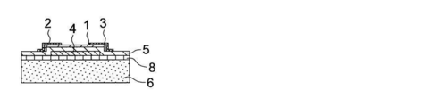
同じく、ボトムゲート・トップコンタクト構成の薄膜トランジスタ素子を作成した(以下、概略断面図を図4で示した)。
同じく、ボトムゲート・トップコンタクト構成の薄膜トランジスタ素子を作成した(以下、概略断面図を図4で示した)。
支持体6としてポリイミドフィルム(厚み200μm)を用い、この上に、先ず、50W/m2/minの条件でコロナ放電処理を施した。その後以下のように接着性向上のため下引き層を形成した。
(下引き層の形成)
下記組成の塗布液を乾燥膜厚2μmになるように塗布し、90℃で5分間乾燥した後、60W/cmの高圧水銀灯下10cmの距離から4秒間硬化させた。
下記組成の塗布液を乾燥膜厚2μmになるように塗布し、90℃で5分間乾燥した後、60W/cmの高圧水銀灯下10cmの距離から4秒間硬化させた。
ジペンタエリスリトールヘキサアクリレート単量体 60g
ジペンタエリスリトールヘキサアクリレート2量体 20g
ジペンタエリスリトールヘキサアクリレート3量体以上の成分 20g
ジエトキシベンゾフェノンUV開始剤 2g
シリコーン系界面活性剤 1g
メチルエチルケトン 75g
メチルプロピレングリコール 75g
さらにその層の上に下記条件で連続的に大気圧プラズマ処理して厚さ50nmの酸化ケイ素膜を設け、これらの層を下引き層8とした。
ジペンタエリスリトールヘキサアクリレート2量体 20g
ジペンタエリスリトールヘキサアクリレート3量体以上の成分 20g
ジエトキシベンゾフェノンUV開始剤 2g
シリコーン系界面活性剤 1g
メチルエチルケトン 75g
メチルプロピレングリコール 75g
さらにその層の上に下記条件で連続的に大気圧プラズマ処理して厚さ50nmの酸化ケイ素膜を設け、これらの層を下引き層8とした。
(使用ガス)
不活性ガス:ヘリウム98.25体積%
反応性ガス:酸素ガス1.5体積%
反応性ガス:テトラエトキシシラン蒸気(ヘリウムガスにてバブリング)0.25体積%
(放電条件)
高周波電源:13.56MHz
放電出力:10W/cm2
(電極条件)
電極は、冷却水による冷却手段を有するステンレス製ジャケットロール母材に対して、セラミック溶射によるアルミナを1mm被覆し、その後、テトラメトキシシランを酢酸エチルで希釈した溶液を塗布乾燥後、紫外線照射により封孔処理を行い、表面を平滑にしてRmax5μmとした誘電体(比誘電率10)を有するロール電極であり、アースされている。一方、印加電極としては、中空の角型のステンレスパイプに対し、上記同様の誘電体を同条件にて被覆した。
不活性ガス:ヘリウム98.25体積%
反応性ガス:酸素ガス1.5体積%
反応性ガス:テトラエトキシシラン蒸気(ヘリウムガスにてバブリング)0.25体積%
(放電条件)
高周波電源:13.56MHz
放電出力:10W/cm2
(電極条件)
電極は、冷却水による冷却手段を有するステンレス製ジャケットロール母材に対して、セラミック溶射によるアルミナを1mm被覆し、その後、テトラメトキシシランを酢酸エチルで希釈した溶液を塗布乾燥後、紫外線照射により封孔処理を行い、表面を平滑にしてRmax5μmとした誘電体(比誘電率10)を有するロール電極であり、アースされている。一方、印加電極としては、中空の角型のステンレスパイプに対し、上記同様の誘電体を同条件にて被覆した。
次いで、ゲート電極を形成する。スパッタ法により、厚さ150nmのITO皮膜を一面に成膜した後、フォトリソグラフ法により、エッチングしてゲート電極4を形成した(図4(2))。
次いで、さらにフィルム温度200℃にて、上述した大気圧プラズマ法により厚さ150nmの酸化珪素膜を設けゲート絶縁層(膜)5を形成した。
次ぎに、ゲート絶縁層上に、以下の方法によりチャネル領域となる部分に半導体層を形成した。
(半導体層の作製)
硝酸インジウム、硝酸亜鉛、硝酸ガリウムを金属比率で1:1:1(モル比)で混合した10質量%水溶液(溶媒は、水/エタノール=9/1(質量比))としたものをインクとしてチャネル形成部にインクジェット塗布し150℃で10分間処理して乾燥し半導体前駆体薄膜を形成した。
硝酸インジウム、硝酸亜鉛、硝酸ガリウムを金属比率で1:1:1(モル比)で混合した10質量%水溶液(溶媒は、水/エタノール=9/1(質量比))としたものをインクとしてチャネル形成部にインクジェット塗布し150℃で10分間処理して乾燥し半導体前駆体薄膜を形成した。
ついで、マルチモードタイプの2.45GHzマイクロ波照射機(四国計測工業(株)製 μ-reactor)を用いて、大気圧条件で、500Wの出力でマイクロ波(2.45GHz)を照射した。マイクロ波の照射中、半導体面側のみ断熱材で保温し、熱電対による表面温度計を用いて、薄膜の表面温度を200℃に保ち、15分間焼成処理を施し半導体層1を形成した。金属酸化物半導体の前駆体の薄膜は透明に変化し金属酸化物薄膜に変換され、半導体層1が形成された(厚さ100nm)
次に、大気雰囲気下、電気炉で、200℃の温度条件で30分、ポストベーク処理を行った。
次に、大気雰囲気下、電気炉で、200℃の温度条件で30分、ポストベーク処理を行った。
〈薄膜トランジスタ素子109の作成〉
薄膜トランジスタ素子108の作成において、ボストベーク処理を電気炉に代えてマイクロ波照射により行って薄膜トランジスタ素子109を作成した。
薄膜トランジスタ素子108の作成において、ボストベーク処理を電気炉に代えてマイクロ波照射により行って薄膜トランジスタ素子109を作成した。
マイクロ波照射は前記2.45GHzマイクロ波照射機(四国計測工業(株)製 μ-reactor)を用いて、大気圧条件で、薄膜の表面温度を200℃に保ち、15分間おこなった。
薄膜トランジスタ素子は、いずれもn型のエンハンスメント動作を示した。各素子について、ドレインバイアスを10Vとし、ゲートバイアスを-10Vから+20Vまで掃引したときのドレイン電流の増加(伝達特性)を観測した。その飽和領域から見積もられた移動度(cm2/Vs)と、on/off比(log値(桁数))、そして閾値(Vth)について評価した。閾値Vthはゲートバイアスに対するドレイン電流値の平方根√Idの関係にて、√Id=0に外挿して得たゲートバイアスの値とした。

作製した各薄膜トランジスタ素子は、いずれもn型のエンハンスメント動作を示したが、マイクロ波によるポストベークによってスパッタ成膜した半導体層の特性バラつきが低減し、その効果がゲート電極にマイクロ波により発熱するITOを用いた時の方が大きいことがわかる。また塗布により半導体前駆体を形成し、その後の焼成処理により半導体を形成し、マイクロ波によるポストベーク処理を行ったものは、特に移動度が高く、また閾値も小さく、特性のバラつきも非常に小さいことがわかる。中でも塗布により半導体前駆体を形成した後、マイクロ波加熱により半導体を形成し、かつマイクロ波でポストベークしたものは特に良好な結果であった。なお、薄膜トランジスタ素子108(電気炉でポストベーク処理をおこなったもの)については、本発明の素子と比べると素子特性が悪いだけでなく、基材の変形(カールやたわみの発生)が発生し、実用上、使用が困難な状態になった。
Claims (8)
- 金属酸化物半導体形成後に、マイクロ波を照射して後加熱を行うことを特徴とする金属酸化物半導体の製造方法。
- 金属酸化物半導体が少なくともIn、Zn、Snのいずれかを含むことを特徴とする請求の範囲第1項に記載の金属酸化物半導体の製造方法。
- 金属酸化物半導体が少なくともGa、Alのいずれかを含むことを特徴とする請求の範囲第1項または第2項に記載の金属酸化物半導体の製造方法。
- 近接または隣接する電極の少なくとも1つの電極にIn、Zn、Snのいずれか1つ以上が含まれることを特徴とする請求の範囲第1項~第3項のいずれか1項に記載の金属酸化物半導体の製造方法。
- 金属酸化物半導体が半導体前駆体を塗布後、半導体変換処理を行うことで形成されることを特徴とする請求の範囲第1項~第4項のいずれか1項に記載の金属酸化物半導体の製造方法。
- 半導体変換処理がマイクロ波(周波数0.3GHz~50GHz)照射であることを特徴とする請求の範囲第5項に記載の金属酸化物半導体の製造方法。
- 半導体前駆体が金属塩であることを特徴とする請求の範囲第5項または第6項に記載の金属酸化物半導体の製造方法。
- 請求の範囲第1項~第7項のいずれか1項に記載の金属酸化物半導体の製造方法で製造された金属酸化物半導体を用いることを特徴とする半導体素子。
Applications Claiming Priority (2)
| Application Number | Priority Date | Filing Date | Title |
|---|---|---|---|
| JP2007-333892 | 2007-12-26 | ||
| JP2007333892 | 2007-12-26 |
Publications (1)
| Publication Number | Publication Date |
|---|---|
| WO2009081968A1 true WO2009081968A1 (ja) | 2009-07-02 |
Family
ID=40801268
Family Applications (1)
| Application Number | Title | Priority Date | Filing Date |
|---|---|---|---|
| PCT/JP2008/073539 Ceased WO2009081968A1 (ja) | 2007-12-26 | 2008-12-25 | 金属酸化物半導体の製造方法およびこれを用いる半導体素子 |
Country Status (2)
| Country | Link |
|---|---|
| JP (1) | JP2009177149A (ja) |
| WO (1) | WO2009081968A1 (ja) |
Cited By (9)
| Publication number | Priority date | Publication date | Assignee | Title |
|---|---|---|---|---|
| WO2010094581A1 (de) * | 2009-02-17 | 2010-08-26 | Evonik Degussa Gmbh | Indiumalkoxid-haltige zusammensetzungen, verfahren zu ihrer herstellung und ihre verwendung |
| JP2012196960A (ja) * | 2011-03-22 | 2012-10-18 | Xerox Corp | プリントヘッドの高密度多層配線方法 |
| WO2014092807A1 (en) * | 2012-12-14 | 2014-06-19 | Board Of Regents, The University Of Texas System | Growing crystalline semiconductor oxide thin films on a substrate at a low temperature using microwave radiation |
| JP2014120712A (ja) * | 2012-12-19 | 2014-06-30 | Ricoh Co Ltd | 金属酸化物膜形成用塗布液、金属酸化物膜、電界効果型トランジスタ、及び電界効果型トランジスタの製造方法 |
| US9748097B2 (en) | 2013-03-29 | 2017-08-29 | Ricoh Company, Ltd. | Coating liquid for forming metal oxide film, metal oxide film, field-effect transistor, and method for producing field-effect transistor |
| JP2018133576A (ja) * | 2009-07-17 | 2018-08-23 | 株式会社半導体エネルギー研究所 | 酸化物半導体膜の作製方法 |
| JP2019220721A (ja) * | 2009-12-25 | 2019-12-26 | 株式会社半導体エネルギー研究所 | 半導体装置およびその作製方法 |
| US20200374993A1 (en) * | 2017-02-28 | 2020-11-26 | Seoul National University R&Db Foundation | Heating system and heating element |
| JP2023157954A (ja) * | 2010-01-20 | 2023-10-26 | 株式会社半導体エネルギー研究所 | 表示装置 |
Families Citing this family (14)
| Publication number | Priority date | Publication date | Assignee | Title |
|---|---|---|---|---|
| TWI830077B (zh) | 2009-08-07 | 2024-01-21 | 日商半導體能源研究所股份有限公司 | 半導體裝置 |
| KR101426723B1 (ko) * | 2009-10-16 | 2014-08-07 | 가부시키가이샤 한도오따이 에네루기 켄큐쇼 | 표시 장치 |
| WO2011052366A1 (en) | 2009-10-30 | 2011-05-05 | Semiconductor Energy Laboratory Co., Ltd. | Voltage regulator circuit |
| KR102450889B1 (ko) * | 2009-12-04 | 2022-10-06 | 가부시키가이샤 한도오따이 에네루기 켄큐쇼 | 반도체 장치 |
| EP2513893A4 (en) * | 2009-12-18 | 2016-09-07 | Semiconductor Energy Lab | Liquid crystal display device and electronic device |
| JP6064314B2 (ja) * | 2010-11-29 | 2017-01-25 | 株式会社リコー | 金属酸化物薄膜形成用塗布液、金属酸化物薄膜の製造方法、及び電界効果型トランジスタの製造方法 |
| WO2013058379A1 (ja) * | 2011-10-21 | 2013-04-25 | 昭和電工株式会社 | マイクロ波加熱装置及びマイクロ波加熱方法 |
| JP5929132B2 (ja) | 2011-11-30 | 2016-06-01 | 株式会社リコー | 金属酸化物薄膜形成用塗布液、金属酸化物薄膜の製造方法、及び電界効果型トランジスタの製造方法 |
| US10375773B2 (en) | 2012-09-25 | 2019-08-06 | Showa Denko K.K. | Microwave heating apparatus |
| KR102090492B1 (ko) | 2013-06-03 | 2020-04-24 | 쇼와 덴코 가부시키가이샤 | 마이크로파 가열용 도전성 수지 조성물 |
| JP6341372B2 (ja) * | 2013-07-18 | 2018-06-13 | 日産化学工業株式会社 | 金属酸化物半導体層形成用前駆体組成物、金属酸化物半導体層の製造方法 |
| JP6828293B2 (ja) | 2015-09-15 | 2021-02-10 | 株式会社リコー | n型酸化物半導体膜形成用塗布液、n型酸化物半導体膜の製造方法、及び電界効果型トランジスタの製造方法 |
| SG11201807957SA (en) | 2016-03-18 | 2018-10-30 | Ricoh Co Ltd | Method for manufacturing a field effect transistor |
| JP2018004830A (ja) * | 2016-06-29 | 2018-01-11 | 日本電信電話株式会社 | 高耐熱性光ファイバモジュールおよびその作製方法 |
Citations (5)
| Publication number | Priority date | Publication date | Assignee | Title |
|---|---|---|---|---|
| JP2000123658A (ja) * | 1998-10-09 | 2000-04-28 | Fuji Photo Film Co Ltd | 透明導電膜の製造方法及び透明導電膜 |
| JP2006013098A (ja) * | 2004-06-25 | 2006-01-12 | Bridgestone Corp | 太陽電池の製造方法 |
| JP2007042689A (ja) * | 2005-07-29 | 2007-02-15 | Fujifilm Holdings Corp | 金属アルコキシド溶液、それを用いた半導体デバイスの製造方法及び半導体デバイス |
| JP2008306176A (ja) * | 2007-05-08 | 2008-12-18 | Tokyo Electron Ltd | 化合物半導体の熱処理方法及びその装置 |
| JP2009004733A (ja) * | 2007-05-18 | 2009-01-08 | Canon Inc | インバータの作製方法及びインバータ |
-
2008
- 2008-12-22 JP JP2008325200A patent/JP2009177149A/ja active Pending
- 2008-12-25 WO PCT/JP2008/073539 patent/WO2009081968A1/ja not_active Ceased
Patent Citations (5)
| Publication number | Priority date | Publication date | Assignee | Title |
|---|---|---|---|---|
| JP2000123658A (ja) * | 1998-10-09 | 2000-04-28 | Fuji Photo Film Co Ltd | 透明導電膜の製造方法及び透明導電膜 |
| JP2006013098A (ja) * | 2004-06-25 | 2006-01-12 | Bridgestone Corp | 太陽電池の製造方法 |
| JP2007042689A (ja) * | 2005-07-29 | 2007-02-15 | Fujifilm Holdings Corp | 金属アルコキシド溶液、それを用いた半導体デバイスの製造方法及び半導体デバイス |
| JP2008306176A (ja) * | 2007-05-08 | 2008-12-18 | Tokyo Electron Ltd | 化合物半導体の熱処理方法及びその装置 |
| JP2009004733A (ja) * | 2007-05-18 | 2009-01-08 | Canon Inc | インバータの作製方法及びインバータ |
Cited By (16)
| Publication number | Priority date | Publication date | Assignee | Title |
|---|---|---|---|---|
| KR20110131179A (ko) * | 2009-02-17 | 2011-12-06 | 에보니크 데구사 게엠베하 | 인듐 알콕시드를 함유하는 조성물, 그의 제조 방법 및 그의 용도 |
| WO2010094581A1 (de) * | 2009-02-17 | 2010-08-26 | Evonik Degussa Gmbh | Indiumalkoxid-haltige zusammensetzungen, verfahren zu ihrer herstellung und ihre verwendung |
| US9115422B2 (en) | 2009-02-17 | 2015-08-25 | Evonik Degussa Gmbh | Compositions containing indium alkoxide, method for the production thereof, and use thereof |
| KR101662862B1 (ko) | 2009-02-17 | 2016-10-05 | 에보니크 데구사 게엠베하 | 인듐 알콕시드를 함유하는 조성물, 그의 제조 방법 및 그의 용도 |
| JP2018133576A (ja) * | 2009-07-17 | 2018-08-23 | 株式会社半導体エネルギー研究所 | 酸化物半導体膜の作製方法 |
| US10256291B2 (en) | 2009-07-17 | 2019-04-09 | Semiconductor Energy Laboratory Co., Ltd. | Method of manufacturing semiconductor device |
| JP2019220721A (ja) * | 2009-12-25 | 2019-12-26 | 株式会社半導体エネルギー研究所 | 半導体装置およびその作製方法 |
| JP2023157954A (ja) * | 2010-01-20 | 2023-10-26 | 株式会社半導体エネルギー研究所 | 表示装置 |
| US12614531B1 (en) | 2010-01-20 | 2026-04-28 | Semiconductor Energy Laboratory Co., Ltd. | Display device |
| JP2012196960A (ja) * | 2011-03-22 | 2012-10-18 | Xerox Corp | プリントヘッドの高密度多層配線方法 |
| KR101819882B1 (ko) * | 2011-03-22 | 2018-01-19 | 제록스 코포레이션 | 프린트 헤드용 고밀도 다중층 상호접속부 |
| WO2014092807A1 (en) * | 2012-12-14 | 2014-06-19 | Board Of Regents, The University Of Texas System | Growing crystalline semiconductor oxide thin films on a substrate at a low temperature using microwave radiation |
| JP2014120712A (ja) * | 2012-12-19 | 2014-06-30 | Ricoh Co Ltd | 金属酸化物膜形成用塗布液、金属酸化物膜、電界効果型トランジスタ、及び電界効果型トランジスタの製造方法 |
| US9748097B2 (en) | 2013-03-29 | 2017-08-29 | Ricoh Company, Ltd. | Coating liquid for forming metal oxide film, metal oxide film, field-effect transistor, and method for producing field-effect transistor |
| US20200374993A1 (en) * | 2017-02-28 | 2020-11-26 | Seoul National University R&Db Foundation | Heating system and heating element |
| US12108513B2 (en) * | 2017-02-28 | 2024-10-01 | Seoul National University R&Db Foundation | Heating system and heating element |
Also Published As
| Publication number | Publication date |
|---|---|
| JP2009177149A (ja) | 2009-08-06 |
Similar Documents
| Publication | Publication Date | Title |
|---|---|---|
| WO2009081968A1 (ja) | 金属酸化物半導体の製造方法およびこれを用いる半導体素子 | |
| JP5644111B2 (ja) | 金属酸化物半導体およびその製造方法、半導体素子、薄膜トランジスタ | |
| JP5763876B2 (ja) | 薄膜トランジスタ、及びその製造方法 | |
| JP2010258057A (ja) | 金属酸化物半導体、その製造方法、及びそれを用いた薄膜トランジスタ | |
| JP2010283190A (ja) | 薄膜トランジスタ、及びその製造方法 | |
| JPWO2009031381A1 (ja) | 金属酸化物半導体の製造方法、及びその方法により得られた薄膜トランジスタ | |
| JP2010098303A (ja) | 金属酸化物前駆体層の作製方法、金属酸化物層の作製方法及び電子デバイス | |
| US20100184253A1 (en) | Process for manufacturing thin film transistor | |
| JP5640323B2 (ja) | 金属酸化物半導体の製造方法、金属酸化物半導体および薄膜トランジスタ | |
| JPWO2009011224A1 (ja) | 金属酸化物半導体の製造方法、それにより得られた薄膜トランジスタ | |
| WO2010061721A1 (ja) | 薄膜トランジスタおよび薄膜トランジスタの製造方法 | |
| JP2010182852A (ja) | 金属酸化物半導体、その製造方法及び薄膜トランジスタ | |
| JP2009065012A (ja) | 薄膜トランジスタ | |
| JP2010093165A (ja) | 電極の製造方法、これを用いた薄膜トランジスタ素子及び有機エレクトロルミネッセンス素子 | |
| JP2011009619A (ja) | 薄膜トランジスタの製造方法及び薄膜トランジスタ | |
| WO2010044332A1 (ja) | 薄膜トランジスタ及びその製造方法 | |
| JP2010147206A (ja) | 薄膜トランジスタ、及びその製造方法 | |
| JP2010258206A (ja) | 金属酸化物半導体の製造方法、金属酸化物半導体及びこれを用いた半導体素子、薄膜トランジスタ | |
| JP2010251591A (ja) | 薄膜トランジスタおよび該薄膜トランジスタの製造方法 | |
| JP2010129742A (ja) | 電子デバイス及びその製造方法 | |
| JP2010258018A (ja) | 半導体薄膜およびこれを用いた薄膜トランジスタ | |
| JP5315822B2 (ja) | 薄膜トランジスタの製造方法及びこれにより製造された電子デバイス | |
| JP2010283002A (ja) | 金属酸化物薄膜パターンの製造方法、金属酸化物薄膜、半導体および薄膜トランジスタ | |
| JPWO2009028452A1 (ja) | 金属酸化物半導体の製造方法およびこれを用い作製された酸化物半導体薄膜を用いた薄膜トランジスタ | |
| JP5578078B2 (ja) | 機能性層の製造方法 |
Legal Events
| Date | Code | Title | Description |
|---|---|---|---|
| 121 | Ep: the epo has been informed by wipo that ep was designated in this application |
Ref document number: 08864408 Country of ref document: EP Kind code of ref document: A1 |
|
| NENP | Non-entry into the national phase |
Ref country code: DE |
|
| NENP | Non-entry into the national phase |
Ref country code: JP |
|
| 122 | Ep: pct application non-entry in european phase |
Ref document number: 08864408 Country of ref document: EP Kind code of ref document: A1 |