WO2004063142A1 - 芳香族アミン誘導体及びそれを用いた有機エレクトロルミネッセンス素子 - Google Patents
芳香族アミン誘導体及びそれを用いた有機エレクトロルミネッセンス素子 Download PDFInfo
- Publication number
- WO2004063142A1 WO2004063142A1 PCT/JP2004/000119 JP2004000119W WO2004063142A1 WO 2004063142 A1 WO2004063142 A1 WO 2004063142A1 JP 2004000119 W JP2004000119 W JP 2004000119W WO 2004063142 A1 WO2004063142 A1 WO 2004063142A1
- Authority
- WO
- WIPO (PCT)
- Prior art keywords
- group
- phenanthroline
- organic
- layer
- amine derivative
- Prior art date
Links
Classifications
-
- C—CHEMISTRY; METALLURGY
- C07—ORGANIC CHEMISTRY
- C07C—ACYCLIC OR CARBOCYCLIC COMPOUNDS
- C07C211/00—Compounds containing amino groups bound to a carbon skeleton
- C07C211/43—Compounds containing amino groups bound to a carbon skeleton having amino groups bound to carbon atoms of six-membered aromatic rings of the carbon skeleton
- C07C211/54—Compounds containing amino groups bound to a carbon skeleton having amino groups bound to carbon atoms of six-membered aromatic rings of the carbon skeleton having amino groups bound to two or three six-membered aromatic rings
-
- C—CHEMISTRY; METALLURGY
- C09—DYES; PAINTS; POLISHES; NATURAL RESINS; ADHESIVES; COMPOSITIONS NOT OTHERWISE PROVIDED FOR; APPLICATIONS OF MATERIALS NOT OTHERWISE PROVIDED FOR
- C09K—MATERIALS FOR MISCELLANEOUS APPLICATIONS, NOT PROVIDED FOR ELSEWHERE
- C09K11/00—Luminescent, e.g. electroluminescent, chemiluminescent materials
- C09K11/06—Luminescent, e.g. electroluminescent, chemiluminescent materials containing organic luminescent materials
-
- H—ELECTRICITY
- H05—ELECTRIC TECHNIQUES NOT OTHERWISE PROVIDED FOR
- H05B—ELECTRIC HEATING; ELECTRIC LIGHT SOURCES NOT OTHERWISE PROVIDED FOR; CIRCUIT ARRANGEMENTS FOR ELECTRIC LIGHT SOURCES, IN GENERAL
- H05B33/00—Electroluminescent light sources
- H05B33/12—Light sources with substantially two-dimensional radiating surfaces
- H05B33/14—Light sources with substantially two-dimensional radiating surfaces characterised by the chemical or physical composition or the arrangement of the electroluminescent material, or by the simultaneous addition of the electroluminescent material in or onto the light source
-
- H—ELECTRICITY
- H10—SEMICONDUCTOR DEVICES; ELECTRIC SOLID-STATE DEVICES NOT OTHERWISE PROVIDED FOR
- H10K—ORGANIC ELECTRIC SOLID-STATE DEVICES
- H10K85/00—Organic materials used in the body or electrodes of devices covered by this subclass
- H10K85/60—Organic compounds having low molecular weight
- H10K85/631—Amine compounds having at least two aryl rest on at least one amine-nitrogen atom, e.g. triphenylamine
- H10K85/633—Amine compounds having at least two aryl rest on at least one amine-nitrogen atom, e.g. triphenylamine comprising polycyclic condensed aromatic hydrocarbons as substituents on the nitrogen atom
-
- C—CHEMISTRY; METALLURGY
- C09—DYES; PAINTS; POLISHES; NATURAL RESINS; ADHESIVES; COMPOSITIONS NOT OTHERWISE PROVIDED FOR; APPLICATIONS OF MATERIALS NOT OTHERWISE PROVIDED FOR
- C09K—MATERIALS FOR MISCELLANEOUS APPLICATIONS, NOT PROVIDED FOR ELSEWHERE
- C09K2211/00—Chemical nature of organic luminescent or tenebrescent compounds
- C09K2211/10—Non-macromolecular compounds
- C09K2211/1003—Carbocyclic compounds
- C09K2211/1014—Carbocyclic compounds bridged by heteroatoms, e.g. N, P, Si or B
-
- H—ELECTRICITY
- H10—SEMICONDUCTOR DEVICES; ELECTRIC SOLID-STATE DEVICES NOT OTHERWISE PROVIDED FOR
- H10K—ORGANIC ELECTRIC SOLID-STATE DEVICES
- H10K2102/00—Constructional details relating to the organic devices covered by this subclass
- H10K2102/10—Transparent electrodes, e.g. using graphene
- H10K2102/101—Transparent electrodes, e.g. using graphene comprising transparent conductive oxides [TCO]
- H10K2102/103—Transparent electrodes, e.g. using graphene comprising transparent conductive oxides [TCO] comprising indium oxides, e.g. ITO
-
- H—ELECTRICITY
- H10—SEMICONDUCTOR DEVICES; ELECTRIC SOLID-STATE DEVICES NOT OTHERWISE PROVIDED FOR
- H10K—ORGANIC ELECTRIC SOLID-STATE DEVICES
- H10K50/00—Organic light-emitting devices
- H10K50/10—OLEDs or polymer light-emitting diodes [PLED]
- H10K50/14—Carrier transporting layers
-
- H—ELECTRICITY
- H10—SEMICONDUCTOR DEVICES; ELECTRIC SOLID-STATE DEVICES NOT OTHERWISE PROVIDED FOR
- H10K—ORGANIC ELECTRIC SOLID-STATE DEVICES
- H10K85/00—Organic materials used in the body or electrodes of devices covered by this subclass
- H10K85/30—Coordination compounds
- H10K85/321—Metal complexes comprising a group IIIA element, e.g. Tris (8-hydroxyquinoline) gallium [Gaq3]
- H10K85/324—Metal complexes comprising a group IIIA element, e.g. Tris (8-hydroxyquinoline) gallium [Gaq3] comprising aluminium, e.g. Alq3
Definitions
- the present invention relates to a novel aromatic amine derivative and an organic electroluminescence device using the same, and more particularly, to an organic EL device in which molecules are less likely to crystallize.
- the present invention relates to a novel aromatic amine derivative which improves the yield in the production of organic EL devices, and an organic electroluminescent device using the same.
- EL organic electroluminescent device
- a fluorescent substance is formed by applying an electric field to recombination energy of holes injected from an anode and electrons injected from a cathode. It is a self-luminous element using the principle of emitting light.
- Eastman Kodak's CW Tang et al. Report on low-voltage driven organic EL devices with stacked devices (W. Tang, SA Vansly ke, Applied Physics Letters, Volume 51, page 9 13) Since 1987, researches on organic EL devices using organic materials as constituent materials have been actively conducted. Tang et al.
- the element structure of the organic EL element includes a hole transport (injection) layer, a two-layer electron transport / emission layer, or a hole transport (injection) layer, a light emitting layer, and an electron transport (injection) layer.
- the three-layer type is well known.
- the present invention has been made to solve the above-mentioned problems, and a novel aromatic amine derivative that is difficult to crystallize and improves the yield when manufacturing an organic EL device, and an organic EL device using the same.
- the purpose is to provide.
- the present inventors have conducted intensive studies to achieve the above object, and as a result, have used a novel aromatic amine derivative having an asymmetric structure represented by the following general formula (1) as a material for an organic EL device.
- the inventors have found that the above problems can be solved when used as a hole transport material, and have completed the present invention.
- the present invention provides an aromatic amine derivative represented by the following general formula (1). .
- a diarylamino group represented by B is a diarylamino group represented by B.
- Ar 1 to Ar 4 are each independently a substituted or unsubstituted aryl group having 5 to 50 nuclear atoms. However, ⁇ and ⁇ are not the same.
- L is a linking group consisting of a substituted or unsubstituted arylene group having 5 to 50 nuclear atoms, or a single bond of a plurality of substituted or unsubstituted arylene groups having 5 to 50 nuclear atoms, oxygen It is a linking group linked by an atom, sulfur atom, nitrogen atom or a saturated or unsaturated divalent aliphatic hydrocarbon group having 1 to 20 nuclear carbon atoms. ),
- the present invention provides an organic EL device in which at least one organic thin film layer including at least one light emitting layer is sandwiched between a cathode and an anode, wherein at least one of the organic thin film layers is the aromatic amine.
- An object of the present invention is to provide an organic EL device containing a derivative alone or as a component of a mixture.
- the aromatic amine derivative of the present invention comprises a compound represented by the following general formula (1).
- a and B are not the same. That is, the aromatic aromatic compound of the present invention
- the min compound has an asymmetric structure.
- a diarylamino group represented by Ar 2 , B is
- Ar 1 to Ar 4 are each independently a substituted or unsubstituted aryl group having 5 to 50 nuclear atoms.
- Examples of the aryl groups of A r ′ to A r 4 include a phenyl group, a 1-naphthyl group, a 2-naphthyl group, a 1-anthryl group, a 2-anthryl group, a 9-anthryl group,
- (2-Phenylpropyl) pyro-1-yl group 2-methyl-1-indolyl group, 4-methyl-1-indolyl group, 2-methyl-13-T-nodolyl group, 4-methyl-3-indolyl group, 1 t
- Examples thereof include a 1-butyl 1-indolyl group, a 4-t-butyl 1-indolyl group, a 2-t-butyl 3-indolyl group, and a 4-t-butyl 3-indolyl group.
- phenyl, naphthyl, biphenyl, anthranyl, phenanthryl, pyrenyl, chrysenyl, fluoranthyl and fluorenyl groups are preferred.
- L represents (I) a substituted or unsubstituted arylene group having 5 to 50 nuclear atoms, or (II) a plurality of substituted or unsubstituted nuclear atoms.
- An arylene group having 5 to 50 children is formed by (II-1) single bond, (II-2) oxygen atom (10_),
- Examples of the arylene group having 5 to 50 nuclear atoms in (I) and (II) include, for example, 1,4-phenylene group, 1,2-phenylene group, 1,3-phenylene group,
- 1,4-phenylene group 1,2-phenylene group, 1,3-phenylene group, 1,4-naphthylene group, 9,10-anthranylene group, 6, 12-Chrysylenelen, 4,4,1-biphenylene, 3,3'-biphenylene,, 2'-biphenylene and 2,7-fluorenylene.
- the saturated or unsaturated divalent aliphatic hydrocarbon group having 1 to 20 nuclear carbon atoms in the above (II-5) may be any of a straight-chain, branched, or cyclic group.
- Examples of the substituted or unsubstituted aryl group having 5 to 50 nuclear atoms include a phenyl group, a 1-naphthyl group, a 2-naphthyl group, a 1-anthryl group, a 2-anthryl group and a 9-anthryl group , 1-phananthryl group, 2-phenanthryl group, 3-phenanthryl group, 4-phenanthryl group, 9-fananthryl group, 1-naphthacenyl group, 2-naphthacenyl group, 9-naphthacenyl group, 1-pyrenyl group, 2-pyrenyl Group, 4-pyrenyl group, 2-biphenylyl group, 3-biphenylyl group, 4-biphenylyl group, p-terphenyl-14-yl group, p-terphenyl-1-yl group, p-terphenyl One 2-yl group, m-terphenyl-1-yl
- Examples of the substituted or unsubstituted alkyl group having 1 to 50 carbon atoms include methyl group, ethyl group, propyl group, isopropyl group, n-butyl group, s-butyl group, isobutyl group, t-butyl group, n-pentyl, n-hexyl, n-heptyl, n-octyl, hydroxymethyl, 1-hydroxyethyl, 2-hydroxyethyl, 2-hydroxyisobutyl, 1,2-dihydroxy Butyl, 1,3-dihydroxyisopropyl, 2,3-dihydroxy-t-butyl, 2,3-trihydroxypropyl, chloromethyl, 1-chloroethyl, 2-chloroethyl, 2-butyl isobutyl, 1,2-dichloroethyl, 1,3-dichloroisopropyl, 2,3-dichloro-t-butyl, 1,2,3
- a substituted or unsubstituted alkoxy group having 1 to 50 carbon atoms is a group represented by OY.
- Y include a methyl group, an ethyl group, a propyl group, an isopropyl group, an n-butyl group, and an s- group.
- Examples of the substituted or unsubstituted aralkyl group having 1 to 50 carbon atoms include benzyl group, 1-phenylethyl group, 2-phenylethyl group, 1-phenylisopropyl group, 2-phenylisopropyl group, and phenyl-t-butyl group.
- -Naphthylisopropyl group 1-naphthylmethyl group, 1-naphthylethyl group, 2-—naphthylethyl group, 1—S—naphthylisopropyl group, 2-naphthylisopropyl group, 1-pyrrolylmethyl group, 2- (1-pyrrolyl) ethyl group, p-methylbenzyl group, m-methylbenzyl group, 0— Methylbenzyl group, p-chlorobenzyl group, m-cyclobenzyl group, 0-benzyl group, p-bromobenzyl group, m-benzyl group Romobenjiru group, 0-blanking opening mode base Nji M-hydroxybenzyl, p-hydroxybenzyl, p-hydroxybenzyl, m-hydroxybenzyl, 0-hydroxybenzyl, p-aminobenzyl, m
- a substituted or unsubstituted aryloxy group having 5 to 50 carbon atoms is represented by 10 Y, and examples of Y ′ are phenyl, 1-naphthyl, 2-naphthyl, 1-anthryl, 2- Anthryl group, 9-anthryl group, 1-phenanthryl group, 2-pentanthryl group, 3-pentanthryl group, 4-pentanthryl group, 9-pentanthryl group, 1-naphthacenyl group, 2-naphthacenyl group, 9-napthacenyl group, 1 — Pyrenyl group, 2-pyrenyl group, 4-pyrenyl group, 2-biphenylyl group, 3 _biphenylyl group, 4-biphenylyl group, ⁇ - evening phenyl-4-yl group, —terphenyl _ 3 —Yl group, ⁇ —N-phenyl-2-yl group, m—Terphenyl 4-
- a substituted or unsubstituted arylthio group having 5 to 50 carbon atoms is represented by 1 SY ", and examples of Y" include phenyl, 1-naphthyl, 2-naphthyl, 1-anthryl, 2-anthryl group, 9-anthryl group, 1-phananthryl group, 2-phenanthryl group, 3-fananthryl group, 4-fananthryl group, 9-phenanthryl group, 1-naphthacenyl group, 2-naphthacenyl group, 9-luff Succinyl group, 1-pyrenyl group, 2-pyrenyl group, 4-pyrenyl group, 2-biphenylyl group, 3-biphenylyl group, 4-biphenylyl group, 4-biphenylyl group, p-terphenyl-2-yl group, p-Evening phenyl -3-yl group, p-Evening phenyl-2-yl group,
- 2-acridinyl group 3-attaridinyl group, 4-attaridinyl group, 9-acridinyl group, 1,7-phenanthroline-1-yl group, 1,7-phenanthroline-1
- a substituted or unsubstituted alkoxy group having 1 to 50 carbon atoms is one C ⁇ 0 Z
- Z include methyl, ethyl, propyl, isopropyl, n-butyl, s-butyl, isobutyl, t-butyl, n-pentyl, n-hexyl, n-heptyl group, n-octyl group, hydroxymethyl group, 1-hydroxyethyl group, 2-hydroxyethyl group, 2-hydroxyisobutyl group, 1,2-dihydroxyethyl group, 1,3-dihydroxyisopropyl Group, 2,3-dihydroxy-t-butyl group, 1,2,3-trihydroxypropyl group, chloromethyl group, 1-chloroethyl group, 2-chloroethyl group, 2-chloroisobutyl group, 1,2 —Dichloroethyl, 1,3-dichloroisopropyl
- An amino group substituted with a substituted or unsubstituted aryl group having 5 to 50 nuclear atoms is represented by — NFQ, and examples of P and Q include a phenyl group, 1 —naphthyl group, and 2— Naphthyl group, 1-anthryl group, 2-anthryl group, 9-anthryl group, 1-phenanthryl group, 2-phenanthryl group, 3-phenanthryl group, 4-phenanthryl group, 9-phenanthryl group, 1-naphthacenyl group, 2-naphthacenyl group, 9-naphthacenyl group, 1-pyrenyl group, 2-pyrenyl group, 4-pyrenyl group, 2-biphenylyl group, 3-biphenylyl group, 4-biphenylyl group, p-biphenylyl group, p-night Phenyl 4-yl group, p-evening phenyl-3-yl group
- the substituents may form a ring with each other.
- the divalent group forming the ring include a tetramethylene group, a pentamethylene group, a hexamethylene group, and diphenylmethane-1,2′-. Diyl group, diphenylethane-1,3,3,1-diyl group, diphenylpropane-1,4,4,1-diyl group and the like.
- halogen atom examples include fluorine, chlorine, bromine, and iodine.
- Specific examples of the aromatic amine derivative represented by the general formula (1) of the present invention are shown below, but it should not be construed that the invention is limited thereto.
- Me represents a methyl group and i Pr represents an isopropyl group.
- the organic EL device of the present invention is an organic EL device in which one or more organic thin film layers including at least a light emitting layer are sandwiched between a cathode and an anode, wherein at least the I layer of the organic thin film layer is The aromatic amine derivative is contained alone or as a component of a mixture.
- the organic thin film layer preferably has a hole transport zone, and the hole transport zone preferably contains the aromatic amine derivative of the present invention alone or as a component of a mixture. More preferably, the organic thin film layer has a hole transport layer, and the hole transport layer contains the aromatic amine derivative of the present invention alone or as a component of a mixture. Furthermore, it is preferable that the hole transport layer contains the aromatic amine derivative of the present invention as a main component.
- Examples of the structure include an anode / insulating layer / hole injection layer / hole transport layer / light emitting layer / electron injection layer / cathode.
- the configuration (8) is usually preferably used, but is not limited thereto.
- the aromatic amine derivative of the present invention may be used for any organic thin film layer of an organic EL device, but can be used for a light emitting band or a hole transporting zone, preferably a hole transporting zone, particularly preferably a hole transporting zone. By using it for the transport layer, molecules are less likely to be crystallized, and the yield in manufacturing an organic EL device is improved.
- the amount of the aromatic amine derivative of the present invention contained in the organic thin film layer is preferably 30 to 100 mol%.
- the organic EL device of the present invention is manufactured on a translucent substrate.
- the translucent substrate referred to here is a substrate that supports the organic EL element, and transmits light in the visible region of 400 to 70 O nm.
- a smooth substrate having an excess ratio of 50% or more is preferable.
- Specific examples include a glass plate and a polymer plate.
- the glass plate include soda lime glass, norium strontium-containing glass, lead glass, aluminogate glass, borosilicate glass, norium borate glass, and quartz.
- the polymer plate include polycarbonate, acrylic, polyethylene terephthalate, polyether sulfide, and polysulfone.
- the anode of the organic EL device of the present invention has a function of injecting holes into the hole transport layer or the light emitting layer, and it is effective that the anode has a work function of 4.5 eV or more.
- Specific examples of the anode material used in the present invention include an indium tin oxide alloy (ITO), tin oxide (NESA), gold, silver, platinum, and copper.
- the anode can be manufactured by forming a thin film from these electrode substances by a method such as an evaporation method or a sputtering method.
- the transmittance of the anode with respect to the light emission be greater than 10%.
- the sheet resistance of the anode is preferably several hundred / portion or less.
- the thickness of the anode depends on the material, but is usually selected in the range of 1 nm to 1 nm, preferably in the range of 10 nm to 200 nm.
- the light emitting layer of the organic EL device has the following functions (1) to (3).
- Injection function A function that can inject holes from the anode or hole injection layer when an electric field is applied, and can inject electrons from the cathode or electron injection layer.
- Light-emitting function Provides a field for recombination of electrons and holes, and connects it to light emission. However, there may be differences between the ease of hole injection and the ease of electron injection.
- the transport capacity represented by the mobility of holes and electrons may be large or small. It is preferable to transfer one of the charges.
- the light emitting layer is particularly preferably a molecular deposition film.
- the molecular deposition film refers to a thin film formed by deposition from a material compound in a gas phase or a film formed by solidification from a material compound in a solution state or a liquid phase. Films can be distinguished from thin films (molecule accumulation films) formed by the LB method by differences in the cohesive structure and higher-order structure, and the resulting functional differences.
- a binder such as a resin and a material compound are dissolved in a solvent to form a solution, which is then subjected to a spin coating method or the like.
- the light emitting layer can also be formed by making the film thinner.
- the light-emitting layer may contain a known light-emitting material other than the light-emitting material comprising the aromatic amine derivative of the present invention, if desired, as long as the object of the present invention is not impaired.
- a light emitting layer containing another known light emitting material may be laminated on the light emitting layer containing the light emitting material comprising the aromatic amine derivative of the present invention.
- the hole injecting / transporting layer is a layer that assists hole injection into the light emitting layer and transports it to the light emitting region, and has a high hole mobility and a small ionization energy of usually 5.5 eV or less.
- a material feed transportation of holes to the emitting layer at a lower electric field strength is preferred, and the mobility of holes, for example, 1 0 4 ⁇ 1 0 6 V / cm during the electric field is applied, preferably it is at least 1 0- 4 cm 2 / V ⁇ sec.
- the aromatic amine derivative of the present invention When the aromatic amine derivative of the present invention is used in the hole transport zone, the aromatic amine derivative of the present invention may be used alone to form a hole injection layer or a layer for transporting a hole, or may be used by mixing with another material. Is also good.
- the material for forming the hole injecting / transporting layer by mixing with the aromatic amine derivative of the present invention is not particularly limited as long as it has the above preferable properties. Any material can be selected from those commonly used as a hole charge transporting material and known materials used for a hole injection layer of an organic EL device.
- JP-A-74-4949, JP-A-60-175052, etc. silazane derivatives (U.S. Pat. Nos. 4,950,950), polysilanes (JP-A-Hei. JP-A No. 2-204996, an aniline-based copolymer (JP-A-2-282263), and a conductive material disclosed in JP-A-1-221139.
- high molecular weight oligomers especially thiophene oligomers).
- the above-mentioned materials can be used, and porphyrin compounds (those disclosed in JP-A-63-2956565) and aromatic tertiary compounds Amine compounds and styrylamine compounds (U.S. Pat. Nos. 4,127,412, JP-A-53-27033, JP-A-54-584345, and 5 4 1 4 9 6 3 4 gazette, 5 4 6 4 2 9 9 gazette, 5 5 7 9 4 5 0 gazette, 5 5-1 4 4 2 5 0 gazette 5 6 1 1 9 1 3 2 and 6 1 2 9 5 5 5 5 8 and 6 1 9 8 3 5 3 and 6 3 2 9 5 6 9 5 It is preferable to use an aromatic tertiary amine compound.
- NPD N- (1-naphthyl) -one N—Hue Nilamino biphenyl
- MTDA TA trifininylamine
- inorganic compounds such as p-type Si and p-type SiC can also be used as the material of the hole injection layer.
- the hole injection / transport layer can be formed by thinning the aromatic amine derivative of the present invention by a known method such as a vacuum evaporation method, a spin coating method, a casting method, and an LB method.
- the thickness of the hole injection / transport layer is not particularly limited, but is usually 5 nm to 5 nm.
- the hole injection / transport layer may be composed of one or more of the above-mentioned materials as long as the hole transport zone contains the aromatic amine derivative of the present invention.
- a layer obtained by laminating a hole injection / transport layer composed of a compound different from the hole injection / transport layer may be used.
- an organic semiconductor layer may be provided as a layer for assisting hole injection or electron injection into the light emitting layer, and a layer having a conductivity of 10- '° S / cm or more is preferable.
- the material for such an organic semiconductor layer include thiophene-containing oligomers and conductive oligomers such as arylamine oligomers disclosed in Japanese Patent Application Laid-Open No. 8-193191. Conductive dendrimers such as arylamine dendrimers can be used.
- the electron injection layer and the transport layer are layers that help inject electrons into the light emitting layer and transport them to the light emitting region.
- the electron mobility is high, and the adhesion improving layer is the cathode in this electron injection layer.
- This is a layer made of a material having good adhesiveness to the material.
- a metal complex of 8-hydroxyquinoline or a derivative thereof is preferable.
- Specific examples of the metal complex of 8-hydroxyquinoline or a derivative thereof include a metal chelate oxinoide compound containing a chelate of oxine (generally, 8-quinolinol or 8-hydroxyquinoline).
- —Quinolinol) Aluminum (Alq) can be used as an electron injection material.
- Examples of the oxaziazole derivative include an electron transfer compound represented by the following general formula.
- Ar 1 ', Ar 2', ⁇ ⁇ 3 ', A r 5', A r 6 ', A r 3' also is respectively substituted properly represents the unsubstituted ⁇ Li Ichiru group, same and Ar 4 ′, Ar 7 ′ and Ar 8 ′ each represent a substituted or unsubstituted arylene group, which may be the same or different Good)
- the aryl group includes a phenyl group, a biphenyl group, an anthranyl group, a perylenyl group, and a pyrenyl group.
- the arylene group includes a phenylene group, a naphthylene group, a biphenylene group, an anthranylene group, a perylene group. Examples include a renylene group and a pyrenylene group.
- the substituent include an alkyl group having 1 to 10 carbon atoms, an alkoxy group having 1 to 10 carbon atoms, and a cyano group.
- the electron transfer compound is preferably a thin film-forming compound.
- the organic EL element of the present invention may contain a reducing dopant in a region for transporting electrons or in an interface region between the cathode and the organic thin film layer.
- the reducing dopant is defined as a substance capable of reducing an electron transporting compound. Therefore, various substances having a certain reducing property are used, for example, alkali metals, alkaline earth metals, rare earth metals, alkali metal oxides, alkali metal halides, and alkaline earth metals. Oxides, alkaline earth metal halides, rare earth metal oxides or rare earth metal halides, alkali metal organic complexes, alkaline earth metal organic complexes, rare earth metal organic complexes At least one substance selected from the group consisting of:
- Preferred examples of the reducing dopant include Na (work function: 2.36 eV), K (work function: 2.28 eV), and Rb (work function: 2.16 eV). And C s
- a more preferred reducing dopant is at least one Al metal which is selected from the group consisting of K, Rb and Cs, more preferably Rb or Cs, and most preferably Is C s.
- alkali metals have particularly high reducing ability, and by adding a relatively small amount to the electron injection region, the emission luminance and the life of the organic EL device can be improved.
- a reducing dopant having a work function of 2.9 eV or less a combination of two or more of these metals is also preferable.
- the organic EL device of the present invention may further include an electron injection layer formed of an insulator or a semiconductor between the cathode and the organic layer.
- an electron injection layer formed of an insulator or a semiconductor between the cathode and the organic layer.
- an insulator at least one metal compound selected from the group consisting of alkali metal chalcogenides, alkaline earth metal chalcogenides, alkali metal halides, and alkali earth metal halides is used. Is preferred.
- the electron injecting layer is composed of such an alkali metal chalcogenide, because the electron injecting property can be further improved.
- alkali metal chalcogenide de for example, L i 2 0, L i O, Na 2 S, include Na 2 S e and NaO, as preferred correct alkaline earth metal chalcogenide de, for example, Ca ⁇ , Ba ⁇ , Sr ⁇ , Be ⁇ , BaS and CaSe.
- Preferred examples of halides of alkali metal include, for example, LiF, NaF, KF, LiC1, KC1, and NaC1.
- the preferred alkaline earth metal halides e.g., such as CaF 2, BaF 2, S r F 2, MgF 2 and B e F 2 Fluoride and halides other than fluoride are mentioned.
- the semiconductor constituting the electron transport layer includes at least Ba, Ca, Sr, Yb, A1, Ga, In, Li, Na.Cd, Mg, Si, Ta, Sb, and Zn.
- An oxide, a nitride, an oxynitride or the like containing one element may be used alone or in combination of two or more.
- the inorganic compound constituting the electron transport layer is a microcrystalline or amorphous insulating thin film. If the electron transport layer is composed of these insulating thin films, a more uniform thin film is formed, so that pixel defects such as dark spots can be reduced. Examples of such inorganic compounds include the above-described alkali metal chalcogenides, alkaline earth metal chalcogenides, halides of alkali metals, and halides of alkali earth metals. (7) Cathode
- a metal, an alloy, an electrically conductive compound having a low work function (4 eV or less), and a mixture thereof as an electrode material are used to inject electrons into the electron transport layer or the light emitting layer.
- an electrode material include sodium, sodium-potassium alloy, magnesium, lithium, magnesium-silver alloy, aluminum / aluminum oxide, aluminum-lithium alloy, indium, rare earth metal and the like.
- This cathode can be manufactured by forming a thin film of these electrode substances by a method such as vapor deposition or sputtering.
- the transmittance of the cathode with respect to the emitted light be greater than 10%.
- the sheet resistance as a cathode is preferably several hundreds ⁇ / b or less, and the film thickness is usually 10 nm to 1 m, preferably 50 to 20 Onm.
- an organic EL element applies an electric field to an ultra-thin film, pixel defects due to leaks and short circuits are likely to occur.
- an insulating thin film layer is provided between a pair of electrodes. Preferably.
- Materials used for the insulating layer include, for example, aluminum oxide, lithium fluoride, lithium oxide, cesium fluoride, cesium oxide, magnesium oxide, magnesium fluoride, calcium oxide, calcium fluoride, aluminum nitride, titanium oxide, Examples include silicon oxide, germanium oxide, silicon nitride, boron nitride, molybdenum oxide, ruthenium oxide, and vanadium oxide, and a mixture or a laminate of these may be used.
- An organic EL element is formed by forming an anode, a light emitting layer, a hole injection / transport layer as needed, and an electron injection / transport layer as needed by the materials and formation methods exemplified above, and further forming a cathode. Can be made. Further, an organic EL device can be manufactured in the reverse order from the cathode to the anode.
- a thin film made of an anode material is formed on a suitable translucent substrate by a method such as vapor deposition or sputtering so as to have a thickness of 1 or less, preferably 10 to 200 nm. Is prepared.
- a hole injection layer is provided on the anode.
- the hole injection layer can be formed by a vacuum deposition method, a spin coating method, a casting method, an LB method, or the like as described above, but a uniform film is easily obtained and pinholes are not easily generated. From the viewpoint of the above, it is preferable to form by a vacuum evaporation method.
- the deposition conditions vary depending on the compound used (the material of the hole injection layer), the crystal structure and the recombination structure of the intended hole injection layer, etc.
- deposition source temperature 5 0 - 4 5 0 ° C vacuum degree of 1 0- 7 ⁇ 1 0- 3 1 0 rr, deposition rate 0 0 1 -. 5 O nm / sec, substrate temperature - 5 0 ⁇ 3 0 0 ° (: It is preferable to appropriately select a film thickness in the range of 5 nm to 5 ⁇ m.
- a light-emitting layer in which a light-emitting layer is provided on the hole-injection layer is also formed using a desired organic light-emitting material by a method such as vacuum evaporation, sputtering, spin coating, or casting.
- a method such as vacuum evaporation, sputtering, spin coating, or casting.
- it can be formed by reducing the thickness of the organic light emitting material, it is preferable to form the film by a vacuum deposition method because a uniform film is easily obtained and a pinhole is hardly generated.
- the evaporation conditions vary depending on the compound used, but can be generally selected from the same condition range as that of the hole injection layer.
- an electron injection layer is provided on the light emitting layer.
- the film is formed by a vacuum evaporation method from the viewpoint of obtaining a uniform film.
- 'Evaporation conditions can be selected from the same condition ranges as for the hole injection layer and the light emitting layer.
- the aromatic amine derivative of the present invention differs depending on which layer of the light-emitting band or the hole-transporting band is contained. However, when a vacuum evaporation method is used, co-evaporation with another material can be performed. . When the spin coating method is used, it can be contained by mixing with other materials.
- the cathode is made of metal, and can be formed by vapor deposition or sputtering. However, vacuum deposition is preferred to protect the underlying organic layer from damage during film formation.
- the organic EL device from the anode to the cathode consistently by one vacuum bow.
- the method for forming each layer of the organic EL device of the present invention is not particularly limited.
- a conventionally known formation method such as a vacuum evaporation method and a spin coating method can be used.
- the organic thin film layer containing the compound represented by the general formula (1) used in the organic EL device of the present invention may be formed by a vacuum evaporation method, a molecular beam evaporation method (MBE method) or a dipping method of a solution dissolved in a solvent. It can be formed by a known method such as a spin coating method, a casting method, a ball coating method, and a mouth coating method.
- each organic layer of the organic EL device of the present invention is not particularly limited. In general, if the thickness is too small, defects such as pinholes are likely to occur. Usually, the efficiency is deteriorated, so that the range of several nm to 1 im is usually preferable.
- the flask was set in an oil bath, and the temperature was gradually raised to 120 ° C while stirring the solution. After 7 hours, the flask was removed from the oil bath to terminate the reaction, and the mixture was left under an argon atmosphere for 12 hours.
- the precipitated crystals were separated by filtration and dried in vacuo at 60 ° C. to obtain 6.73 g of N, N-di (4-biphenylyl) -benzylamine.
- the obtained solution was transferred to a separating funnel, washed with 50 ml of a saturated aqueous solution of sodium hydrogencarbonate, the organic layer was separated, and dried with anhydrous carbon dioxide. After filtration, the solvent was distilled off, and the obtained residue was recrystallized by adding 50 ml of toluene. The precipitated crystals were separated by filtration and dried in vacuum at 50 ° C. to obtain 0.99 g of di-4-biphenylylamine.
- di-41-biphenylamine 10g (Tokyo Kasei), 4, 4 "- Dibromo-p-terphenyl 12.
- lg Lithyl
- t-butoxy sodium 3 g Hiroshima Wako
- bis (triphenylphosphine) palladium chloride (II) 0.5 g (Tokyo Kasei) And 500 ml of xylene, and reacted at 130 ° C. for 24 hours.
- the 4, -promoter N, N-gibi obtained in (1) of Example 2 was used.
- the flask was set in an oil bath, and the temperature was gradually raised to 120 ° C while stirring the solution. After 7 hours, the flask was removed from the oil bath to terminate the reaction, and the mixture was left under an argon atmosphere for 12 hours.
- the precipitated crystals were separated by filtration and dried in a vacuum at 60 ° C. to obtain 6.12 g of N, N-di (4,1-methyl-4-4-biphenylyl) -1-benzylamine.
- the obtained solution was transferred to a separating funnel, washed with 50 ml of a saturated aqueous solution of sodium hydrogen carbonate, and the organic layer was separated and dried with anhydrous potassium carbonate. After filtration, the solvent was distilled off, and the obtained residue was recrystallized by adding 50 ml of toluene. The precipitated crystals were separated by filtration and dried in a vacuum at 50 t to give 0.83 g of di (4′-methyl-4-biphenylyl) amine.
- a 25ramX75mmXL 1mm thick glass substrate with an IT0 transparent electrode (manufactured by Jishmatic) was subjected to ultrasonic cleaning in isopropyl alcohol for 5 minutes, and then UV ozone cleaning for 30 minutes.
- the glass substrate with the transparent electrode lines after cleaning is mounted on a substrate holder of a vacuum evaporation apparatus.
- 1, N-bis (N, N, diphenyl-4-aminophenyl) 1N, N-diphenyl-1,4'-diamino-1, ⁇ ⁇ -biphenyl film (TPD232 film) was formed.
- This TPD 232 film functions as a hole injection layer.
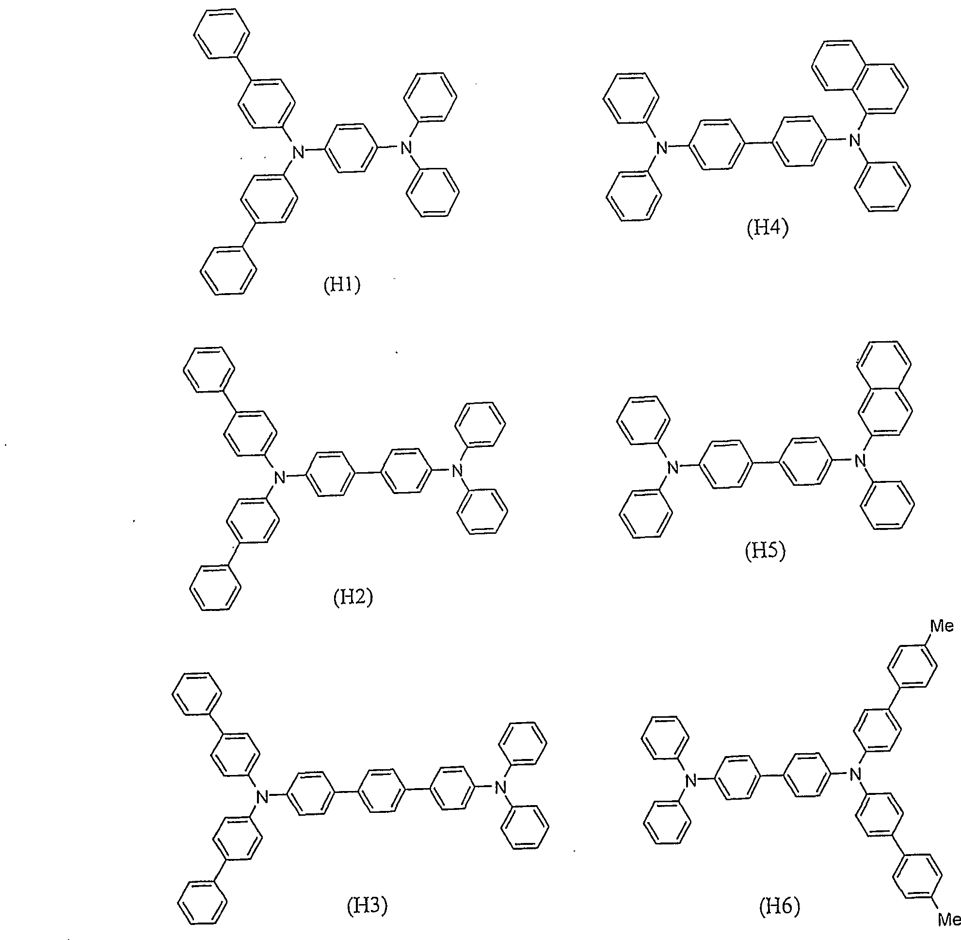
- a 20 nm-thick compound (H 1) layer was formed as a hole transport material.
- This film functions as a hole transport layer.
- the following compound E Ml having a thickness of 40 nm was vapor-deposited to form a film.
- the following amine compound D1 having a styryl group was deposited as a light emitting molecule so that the weight ratio of EM1: D1 was 40: 2.
- This film functions as a light emitting layer.
- the following A1q film having a thickness of lOnm was formed on this film. This functions as an electron injection layer.
- a reducing dopant Li Li source: manufactured by SAES Getter Co., Ltd.
- Alq Alq are binary deposited
- an A1q: Li film (film thickness lOrai) is formed as an electron injection layer (or cathode).
- This A 1 q Metal A on the Li film 1 was deposited to form a metal cathode to form an organic EL device.
- the compound (H 1) was highly amorphous, and the crystal did not block the opening of the evaporation source during the evaporation. .
- An organic EL device was fabricated in the same manner as in Example 7, except that the compound (H 2) was used instead of the compound (H 1).
- the compound (H 2) was highly amorphous, and the crystal did not block the opening of the vapor deposition source during vapor deposition.
- An organic EL device was fabricated in the same manner as in Example 7, except that the compound (H 3) was used instead of the compound (H I).
- the luminous efficiency of the obtained device at a current density of 1 mA / cm 2 was measured. Is shown in Table 1.
- the compound (H 3) was highly amorphous, and the crystals did not block the opening of the evaporation source during deposition.
- An organic EL device was fabricated in the same manner as in Example 7, except that the compound (H4) was used instead of the compound (H I).
- the luminous efficiency of the obtained device was measured at a current density of lmA / cm 2 , and the results are shown in Table 1.
- the compound (H 4) was highly amorphous, and the crystal did not block the opening of the evaporation source during evaporation.
- An organic EL device was fabricated in the same manner as in Example 7, except that the compound (H 5) was used instead of the compound (H I).
- the luminous efficiency of the obtained device was measured at a current density of lmA / cm 2 , and the results are shown in Table 1.
- the compound (H 5) was highly amorphous, and the crystal did not block the opening of the evaporation source during evaporation.
- An organic EL device was fabricated in the same manner as in Example 7, except that the compound (H6) was used instead of the compound (H I).
- the luminous efficiency of the obtained device was measured at a current density of lmA / cm 2 , and the results are shown in Table 1.
- the compound (H 6) had a high amorphous property, and the crystal did not block the opening of the evaporation source during the evaporation.
- Example 7 instead of compound (HI), the following N, N, ⁇ ′, ⁇ ′—tetra (4-Biphenyl) An organic EL device was fabricated in the same manner except that diaminobiphenylene (TBDB) was used.
- TBDB diaminobiphenylene
- TBDB has high crystallinity, and crystallized at the opening of the evaporation source during evaporation, so that a continuous film could not be formed.
- the aromatic amine derivative of the present invention when used as a hole transporting material for an organic EL device, it is possible to emit light with the same luminous efficiency as that of a conventionally used material.
- the amorphous property is high, the element can be formed continuously without blocking the opening of the evaporation source at the time of film formation, which is extremely effective in improving the production yield of the organic EL element.
Landscapes
- Chemical & Material Sciences (AREA)
- Organic Chemistry (AREA)
- Engineering & Computer Science (AREA)
- Materials Engineering (AREA)
- Physics & Mathematics (AREA)
- Spectroscopy & Molecular Physics (AREA)
- Optics & Photonics (AREA)
- Inorganic Chemistry (AREA)
- Electroluminescent Light Sources (AREA)
- Organic Low-Molecular-Weight Compounds And Preparation Thereof (AREA)
Abstract
Description


Claims

Priority Applications (2)
| Application Number | Priority Date | Filing Date | Title |
|---|---|---|---|
| US10/542,105 US20060134458A1 (en) | 2003-01-16 | 2004-01-09 | Aromatic amine derivative and organic electroluminescence element |
| EP04701092A EP1584614A4 (en) | 2003-01-16 | 2004-01-09 | AROMATIC AMINE DERIVATIVE AND ORGANIC ELECTROLUMINESCENT ELEMENT |
Applications Claiming Priority (2)
| Application Number | Priority Date | Filing Date | Title |
|---|---|---|---|
| JP2003-007762 | 2003-01-16 | ||
| JP2003007762A JP2004262761A (ja) | 2003-01-16 | 2003-01-16 | 芳香族アミン誘導体及びそれを用いた有機エレクトロルミネッセンス素子 |
Related Child Applications (1)
| Application Number | Title | Priority Date | Filing Date |
|---|---|---|---|
| US12/170,252 Continuation US7732042B2 (en) | 2003-08-22 | 2008-07-09 | Laminated glass and interlayer film for laminated glasses |
Publications (1)
| Publication Number | Publication Date |
|---|---|
| WO2004063142A1 true WO2004063142A1 (ja) | 2004-07-29 |
Family
ID=32709135
Family Applications (1)
| Application Number | Title | Priority Date | Filing Date |
|---|---|---|---|
| PCT/JP2004/000119 WO2004063142A1 (ja) | 2003-01-16 | 2004-01-09 | 芳香族アミン誘導体及びそれを用いた有機エレクトロルミネッセンス素子 |
Country Status (7)
| Country | Link |
|---|---|
| US (1) | US20060134458A1 (ja) |
| EP (1) | EP1584614A4 (ja) |
| JP (1) | JP2004262761A (ja) |
| KR (1) | KR101026627B1 (ja) |
| CN (1) | CN100526288C (ja) |
| TW (1) | TW200500440A (ja) |
| WO (1) | WO2004063142A1 (ja) |
Cited By (2)
| Publication number | Priority date | Publication date | Assignee | Title |
|---|---|---|---|---|
| WO2006073054A1 (ja) | 2005-01-05 | 2006-07-13 | Idemitsu Kosan Co., Ltd. | 芳香族アミン誘導体及びそれを用いた有機エレクトロルミネッセンス素子 |
| JP5203207B2 (ja) * | 2006-08-23 | 2013-06-05 | 出光興産株式会社 | 芳香族アミン誘導体及びそれらを用いた有機エレクトロルミネッセンス素子 |
Families Citing this family (21)
| Publication number | Priority date | Publication date | Assignee | Title |
|---|---|---|---|---|
| JP2006100756A (ja) * | 2003-11-07 | 2006-04-13 | Sony Corp | 有機電界発光素子および表示装置 |
| JP2006096964A (ja) * | 2003-11-07 | 2006-04-13 | Sony Corp | 有機発光材料および有機材料の製造方法 |
| KR101030008B1 (ko) * | 2004-12-31 | 2011-04-20 | 삼성모바일디스플레이주식회사 | 유기 전계 발광 소자 |
| KR20070091183A (ko) | 2005-01-05 | 2007-09-07 | 이데미쓰 고산 가부시키가이샤 | 방향족 아민 유도체 및 이를 이용한 유기 전기발광 소자 |
| JP5040062B2 (ja) * | 2005-01-17 | 2012-10-03 | コニカミノルタホールディングス株式会社 | 有機エレクトロルミネッセンス素子、照明装置及び表示装置 |
| JP4667926B2 (ja) * | 2005-03-30 | 2011-04-13 | 出光興産株式会社 | 芳香族アミン誘導体及びそれを用いた有機エレクトロルミネッセンス素子 |
| TWI361018B (en) * | 2005-04-18 | 2012-03-21 | Sony Corp | Display device and a method of manufacturing the s |
| JP5103727B2 (ja) * | 2005-11-16 | 2012-12-19 | 東ソー株式会社 | フルオレン化合物およびそれを用いた有機el素子 |
| EP1995234B1 (en) * | 2006-01-25 | 2016-01-06 | Hodogaya Chemical Co., Ltd. | p-TERPHENYL COMPOUND MIXTURE AND ELECTROPHOTOGRAPHIC PHOTORECEPTORS MADE BY USING THE SAME |
| JP4795268B2 (ja) | 2006-04-20 | 2011-10-19 | キヤノン株式会社 | 有機発光素子 |
| JP5616582B2 (ja) * | 2006-06-22 | 2014-10-29 | 出光興産株式会社 | 複素環含有アリールアミン誘導体を用いた有機エレクトロルミネッセンス素子 |
| JP5109303B2 (ja) * | 2006-07-31 | 2012-12-26 | ソニー株式会社 | 有機発光素子および表示装置 |
| JP2008069120A (ja) * | 2006-09-15 | 2008-03-27 | Idemitsu Kosan Co Ltd | 芳香族アミン誘導体及びそれらを用いた有機エレクトロルミネッセンス素子 |
| EP2423179A4 (en) * | 2009-04-24 | 2012-10-24 | Idemitsu Kosan Co | AROMATIC AMINE DERIVATIVE AND ORGANIC ELECTROLUMINESCENT ELEMENT CONTAINING THE SAME |
| CN103805164B (zh) * | 2012-11-14 | 2015-04-15 | 吉林奥来德光电材料股份有限公司 | 一种苯并蒽类有机发光材料及其制备方法和应用 |
| JP6788335B2 (ja) | 2014-08-11 | 2020-11-25 | 三星ディスプレイ株式會社Samsung Display Co.,Ltd. | 有機エレクトロルミネッセンス素子用モノアミン材料及びそれを用いた有機エレクトロルミネッセンス素子 |
| GB2541764B (en) | 2015-04-15 | 2018-04-11 | Ocado Innovation Ltd | System and method for configuration of buildings or storage |
| KR102563713B1 (ko) | 2017-04-26 | 2023-08-07 | 오티아이 루미오닉스 인크. | 표면의 코팅을 패턴화하는 방법 및 패턴화된 코팅을 포함하는 장치 |
| US11751415B2 (en) | 2018-02-02 | 2023-09-05 | Oti Lumionics Inc. | Materials for forming a nucleation-inhibiting coating and devices incorporating same |
| WO2020178804A1 (en) | 2019-03-07 | 2020-09-10 | Oti Lumionics Inc. | Materials for forming a nucleation-inhibiting coating and devices incorporating same |
| JP2023553379A (ja) | 2020-12-07 | 2023-12-21 | オーティーアイ ルミオニクス インコーポレーテッド | 核形成抑制被膜及び下地金属被膜を用いた導電性堆積層のパターニング |
Citations (2)
| Publication number | Priority date | Publication date | Assignee | Title |
|---|---|---|---|---|
| JP2000056490A (ja) * | 1998-08-10 | 2000-02-25 | Canon Inc | 電子写真感光体、プロセスカートリッジ及び電子写真装置 |
| EP1195422A1 (en) * | 1999-12-20 | 2002-04-10 | Matsushita Electric Industrial Co., Ltd. | Thin film el device |
Family Cites Families (13)
| Publication number | Priority date | Publication date | Assignee | Title |
|---|---|---|---|---|
| WO1995009147A1 (fr) * | 1993-09-29 | 1995-04-06 | Idemitsu Kosan Co., Ltd. | Element electroluminescent organique et derive d'arylenediamine |
| JP3828595B2 (ja) * | 1994-02-08 | 2006-10-04 | Tdk株式会社 | 有機el素子 |
| EP0666298A3 (en) * | 1994-02-08 | 1995-11-15 | Tdk Corp | Organic electroluminescent element and compound used therein. |
| US5681664A (en) * | 1994-08-04 | 1997-10-28 | Toyo Ink Manufacturing Co., Ltd. | Hole-transporting material and use thereof |
| CN1152607C (zh) * | 1995-01-19 | 2004-06-02 | 出光兴产株式会社 | 有机电致发光装置,有机薄膜和三胺化合物 |
| WO1998030071A1 (fr) * | 1996-12-28 | 1998-07-09 | Tdk Corporation | Elements electroluminescents organiques |
| DE69804529T2 (de) * | 1997-05-19 | 2002-10-02 | Canon Kk | Organisches Material und elektrolumineszente Vorrichtung dasselbe nutzend |
| JP3985311B2 (ja) * | 1997-10-20 | 2007-10-03 | チッソ株式会社 | アミン誘導体及びそれを用いた有機電界発光素子 |
| DE19829948A1 (de) * | 1998-07-04 | 2000-01-05 | Bayer Ag | Elektrolumineszierende Anordnung unter Verwendung von Azomethin-Metallkomplexen |
| JP3895178B2 (ja) * | 1999-09-30 | 2007-03-22 | 出光興産株式会社 | アミン化合物及びそれを用いた有機エレクトロルミネッセンス素子 |
| JP3614365B2 (ja) * | 1999-12-20 | 2005-01-26 | 松下電器産業株式会社 | 薄膜el素子 |
| JP3998903B2 (ja) * | 2000-09-05 | 2007-10-31 | 出光興産株式会社 | 新規アリールアミン化合物及び有機エレクトロルミネッセンス素子 |
| DE10203328A1 (de) * | 2002-01-28 | 2003-08-07 | Syntec Ges Fuer Chemie Und Tec | Neue Triarylamin-Derivate mit raumfüllenden Flügelgruppen und ihre Einsatz in elektro-fotografischen und organischen elektrolumineszenten Vorrichtungen |
-
2003
- 2003-01-16 JP JP2003007762A patent/JP2004262761A/ja active Pending
-
2004
- 2004-01-09 WO PCT/JP2004/000119 patent/WO2004063142A1/ja active Application Filing
- 2004-01-09 KR KR1020057013051A patent/KR101026627B1/ko active IP Right Grant
- 2004-01-09 CN CNB200480006742XA patent/CN100526288C/zh not_active Expired - Lifetime
- 2004-01-09 US US10/542,105 patent/US20060134458A1/en not_active Abandoned
- 2004-01-09 EP EP04701092A patent/EP1584614A4/en not_active Withdrawn
- 2004-01-15 TW TW093101059A patent/TW200500440A/zh unknown
Patent Citations (2)
| Publication number | Priority date | Publication date | Assignee | Title |
|---|---|---|---|---|
| JP2000056490A (ja) * | 1998-08-10 | 2000-02-25 | Canon Inc | 電子写真感光体、プロセスカートリッジ及び電子写真装置 |
| EP1195422A1 (en) * | 1999-12-20 | 2002-04-10 | Matsushita Electric Industrial Co., Ltd. | Thin film el device |
Non-Patent Citations (4)
| Title |
|---|
| KOENE B.E. ET AL: "Unsymmetrical triaryldiamines as thermally stable hole transporting layers for organic light-emitting devices", CHEMISTRY OF MATERIALS, vol. 10, no. 8, 1998, pages 2235 - 2250, XP002979930 * |
| O'BRIEN D.F. ET AL.: "Hole transporting materials with high glass transition temperatures for use in organic light-emitting devices", ADVANCED MATERIALS, vol. 10, no. 14, 1998, pages 1108 - 1112, XP000781874 * |
| See also references of EP1584614A4 * |
| TOKITO S. ET AL.: "Thermal stability of electroluminescent devices fabricated using novel charge-transporting materials", POLYMER PREPRINTS, vol. 38, no. 1, 1997, pages 388 - 389, XP002979931 * |
Cited By (11)
| Publication number | Priority date | Publication date | Assignee | Title |
|---|---|---|---|---|
| WO2006073054A1 (ja) | 2005-01-05 | 2006-07-13 | Idemitsu Kosan Co., Ltd. | 芳香族アミン誘導体及びそれを用いた有機エレクトロルミネッセンス素子 |
| EP1834945A1 (en) * | 2005-01-05 | 2007-09-19 | Idemitsu Kosan Co., Ltd. | Aromatic amine derivative and organic electroluminescent device using same |
| EP1834945A4 (en) * | 2005-01-05 | 2009-04-15 | Idemitsu Kosan Co | AROMATIC AMINE DERIVATIVE AND ORGANIC ELECTROLUMINESCENT DEVICE USING THE SAME |
| EP2371810A1 (en) * | 2005-01-05 | 2011-10-05 | Idemitsu Kosan Co., Ltd. | Aromatic amine derivative and organic electroluminescent device using same |
| US20120184776A1 (en) * | 2005-01-05 | 2012-07-19 | Idemitsu Kosan Co., Ltd. | Aromatic amine derivative and organic electroluminescent device using same |
| KR101169901B1 (ko) | 2005-01-05 | 2012-07-31 | 이데미쓰 고산 가부시키가이샤 | 방향족 아민 유도체 및 이를 이용한 유기 전기발광 소자 |
| CN1984874B (zh) * | 2005-01-05 | 2012-09-26 | 出光兴产株式会社 | 芳香族胺衍生物及使用了它的有机电致发光元件 |
| KR101192463B1 (ko) * | 2005-01-05 | 2012-10-17 | 이데미쓰 고산 가부시키가이샤 | 방향족 아민 유도체 및 이를 이용한 유기 전기발광 소자 |
| US8883324B2 (en) | 2005-01-05 | 2014-11-11 | Idemitsu Kosan Co., Ltd. | Aromatic amine derivative and organic electroluminescent device using same |
| JP5203207B2 (ja) * | 2006-08-23 | 2013-06-05 | 出光興産株式会社 | 芳香族アミン誘導体及びそれらを用いた有機エレクトロルミネッセンス素子 |
| US9112167B2 (en) | 2006-08-23 | 2015-08-18 | Idemitsu Kosan Company, Limited | Aromatic amine derivatives and organic electroluminescent device using same |
Also Published As
| Publication number | Publication date |
|---|---|
| EP1584614A4 (en) | 2007-03-14 |
| KR101026627B1 (ko) | 2011-04-04 |
| CN1759094A (zh) | 2006-04-12 |
| JP2004262761A (ja) | 2004-09-24 |
| CN100526288C (zh) | 2009-08-12 |
| US20060134458A1 (en) | 2006-06-22 |
| TW200500440A (en) | 2005-01-01 |
| KR20050095848A (ko) | 2005-10-04 |
| EP1584614A1 (en) | 2005-10-12 |
Similar Documents
| Publication | Publication Date | Title |
|---|---|---|
| US11538997B2 (en) | Aromatic amine derivative and electroluminescence device using the same | |
| JP5317386B2 (ja) | 含窒素複素環誘導体及びそれを用いた有機エレクトロルミネッセンス素子 | |
| JP4955622B2 (ja) | 芳香族アミン誘導体及びそれを用いた有機エレクトロルミネッセンス素子 | |
| JP5186365B2 (ja) | 芳香族アミン誘導体及びそれらを用いた有機エレクトロルミネッセンス素子 | |
| JP4955402B2 (ja) | 芳香族アミン誘導体及びそれを用いた有機エレクトロルミネッセンス素子 | |
| JP5258562B2 (ja) | 芳香族アミン誘導体及びそれらを用いた有機エレクトロルミネッセンス素子 | |
| JP2007153778A (ja) | 含窒素複素環誘導体及びそれを用いた有機エレクトロルミネッセンス素子 | |
| KR101026627B1 (ko) | 방향족 아민 유도체 및 이를 이용한 유기 전기발광 소자 | |
| JPWO2007007463A1 (ja) | 電子吸引性置換基を有する含窒素複素環誘導体及びそれを用いた有機エレクトロルミネッセンス素子 | |
| WO2004041774A1 (ja) | 芳香族アミン誘導体及びそれを用いた有機エレクトロルミネッセンス素子 | |
| JPWO2007111263A1 (ja) | 含窒素複素環誘導体及びそれを用いた有機エレクトロルミネッセンス素子 | |
| JPWO2007007464A1 (ja) | 含窒素複素環誘導体及びそれを用いた有機エレクトロルミネッセンス素子 | |
| JP2008069120A (ja) | 芳香族アミン誘導体及びそれらを用いた有機エレクトロルミネッセンス素子 | |
| JP2008150310A (ja) | 芳香族アミン誘導体及びそれらを用いた有機エレクトロルミネッセンス素子 | |
| JP2007039406A (ja) | 含窒素複素環誘導体及びそれを用いた有機エレクトロルミネッセンス素子 | |
| JPWO2007111262A1 (ja) | 含窒素複素環誘導体及びそれを用いた有機エレクトロルミネッセンス素子 | |
| JP2008007424A (ja) | 芳香族アミン誘導体及びそれらを用いた有機エレクトロルミネッセンス素子 | |
| JP2007063220A (ja) | 含窒素複素環誘導体及びそれを用いた有機エレクトロルミネッセンス素子 | |
| JP5523486B2 (ja) | 含窒素複素環誘導体及びそれを用いた有機エレクトロルミネッセンス素子 |
Legal Events
| Date | Code | Title | Description |
|---|---|---|---|
| AK | Designated states |
Kind code of ref document: A1 Designated state(s): AE AG AL AM AT AU AZ BA BB BG BR BW BY BZ CA CH CN CO CR CU CZ DE DK DM DZ EC EE EG ES FI GB GD GE GH GM HR HU ID IL IN IS KE KG KP KR KZ LC LK LR LS LT LU LV MA MD MG MK MN MW MX MZ NA NI NO NZ OM PG PH PL PT RO RU SC SD SE SG SK SL SY TJ TM TN TR TT TZ UA UG US UZ VC VN YU ZA ZM ZW |
|
| AL | Designated countries for regional patents |
Kind code of ref document: A1 Designated state(s): BW GH GM KE LS MW MZ SD SL SZ TZ UG ZM ZW AM AZ BY KG KZ MD RU TJ TM AT BE BG CH CY CZ DE DK EE ES FI FR GB GR HU IE IT LU MC NL PT RO SE SI SK TR BF BJ CF CG CI CM GA GN GQ GW ML MR NE SN TD TG |
|
| 121 | Ep: the epo has been informed by wipo that ep was designated in this application | ||
| WWE | Wipo information: entry into national phase |
Ref document number: 2004701092 Country of ref document: EP |
|
| ENP | Entry into the national phase |
Ref document number: 2006134458 Country of ref document: US Kind code of ref document: A1 |
|
| WWE | Wipo information: entry into national phase |
Ref document number: 10542105 Country of ref document: US |
|
| WWE | Wipo information: entry into national phase |
Ref document number: 1020057013051 Country of ref document: KR |
|
| WWE | Wipo information: entry into national phase |
Ref document number: 1621/CHENP/2005 Country of ref document: IN |
|
| WWE | Wipo information: entry into national phase |
Ref document number: 2004806742X Country of ref document: CN |
|
| WWP | Wipo information: published in national office |
Ref document number: 1020057013051 Country of ref document: KR |
|
| WWP | Wipo information: published in national office |
Ref document number: 2004701092 Country of ref document: EP |
|
| WWP | Wipo information: published in national office |
Ref document number: 10542105 Country of ref document: US |