US9917585B2 - Data output circuit and method for driving the same - Google Patents
Data output circuit and method for driving the same Download PDFInfo
- Publication number
- US9917585B2 US9917585B2 US13/935,931 US201313935931A US9917585B2 US 9917585 B2 US9917585 B2 US 9917585B2 US 201313935931 A US201313935931 A US 201313935931A US 9917585 B2 US9917585 B2 US 9917585B2
- Authority
- US
- United States
- Prior art keywords
- data transmission
- data
- charges
- capacitor
- transmission line
- Prior art date
- Legal status (The legal status is an assumption and is not a legal conclusion. Google has not performed a legal analysis and makes no representation as to the accuracy of the status listed.)
- Active, expires
Links
Images


Classifications
-
- G—PHYSICS
- G11—INFORMATION STORAGE
- G11C—STATIC STORES
- G11C5/00—Details of stores covered by group G11C11/00
- G11C5/14—Power supply arrangements, e.g. power down, chip selection or deselection, layout of wirings or power grids, or multiple supply levels
-
- H—ELECTRICITY
- H03—ELECTRONIC CIRCUITRY
- H03K—PULSE TECHNIQUE
- H03K19/00—Logic circuits, i.e. having at least two inputs acting on one output; Inverting circuits
- H03K19/0175—Coupling arrangements; Interface arrangements
- H03K19/017509—Interface arrangements
-
- G—PHYSICS
- G11—INFORMATION STORAGE
- G11C—STATIC STORES
- G11C7/00—Arrangements for writing information into, or reading information out from, a digital store
- G11C7/10—Input/output [I/O] data interface arrangements, e.g. I/O data control circuits, I/O data buffers
Definitions
- Exemplary embodiments of the present invention relate to a semiconductor device, and more particularly, to a data output circuit and a method for driving the same.
- a semiconductor device including a double data rate synchronous dynamic random access memory receives a command, an address and data from an external controller and performs a read operation and a write operation.
- DDR SDRAM double data rate synchronous dynamic random access memory
- circuits for inputting and outputting a command, an address, and data may be disposed in both of the external controller and the semiconductor device.
- FIG. 1 is a block diagram illustrating a conventional data exchange system.
- a conventional data exchange system includes a first semiconductor device 110 and a second semiconductor device 120 .
- the first semiconductor device 110 includes a first output driving unit 111 and a first input driving unit 112 .
- the second semiconductor device 120 includes a second output driving unit 121 and a second input driving unit 122 .
- An output data DAT_OUT_ 01 of the first semiconductor device 110 is inputted to the first output driving unit 111 .
- the first output driving unit 111 transfers the output data DAT_OUT_ 01 to the second semiconductor device 120 through a data transmission line DQ.
- the second input driving unit 122 of the second semiconductor device 120 receives the output data DAT_OUT_ 01 of the first semiconductor device 110 through the data transmission line DQ, and outputs an input data DAT_IN_ 02 of the second semiconductor device 120 , which is used in various performances of the second semiconductor device 120 .
- An output data DAT_OUT_ 02 of the second semiconductor device 120 is inputted to the second output driving unit 121 .
- the second output driving unit 121 transfers the output data DAT_OUT_ 02 to the first semiconductor device 110 through the data transmission line DQ.
- the first input driving unit 112 of the first semiconductor device 110 receives the output data DAT_OUT_ 02 of the second semiconductor device 120 through the data transmission line DQ, and outputs an input data DAT_IN_ 01 of the first semiconductor device 110 , which is used in various performances of the second semiconductor device 110 .
- a semiconductor device has been developed to operate at a high speed and with a low power.
- it is widely used to increase a number of data lines or raise an operation frequency to implement a high speed operation of the semiconductor device.
- Exemplary embodiments of the present invention are directed to a data output circuit and a method for driving the same to reuse an energy used for transferring data in a data transmission operation.
- embodiments of the present invention are directed to a multi-chip package including a data output circuit for reusing an energy used for transferring data in a data transmission operation.
- a data output circuit includes a data driving unit suitable for driving a data transmission line with a driving voltage corresponding to data during a data transmission operation, and a charging/discharging unit suitable for storing charges on the data transmission line and reuse the stored charges as the driving voltage.
- a method for driving an output data circuit includes driving a data transmission line with a driving voltage corresponding to data to be outputted to transmit the data, performing a charging operation using charges on the data transmission line to generate a recovery power driving voltage, after the driving of the data transmission line, and driving the data transmission line with at least the recovery power driving voltage to transmit the data.
- a data output circuit includes a plurality of data driving units suitable for receiving a plurality of driving voltages, and driving each of a plurality of data transmission lines with a driving voltage corresponding to data among the plurality of driving voltages during a data transmission operation, and a common charging unit suitable for being shared by the plurality of data transmission lines, storing charges on the plurality of data transmission lines as a recovery power driving voltage, and providing the recovery power driving voltage as one of the plurality of driving voltages.
- a multi-chip package includes a plurality of slave chips suitable for outputting data having a multi-level through a plurality of data transmission through-chip-vias, a master chip suitable for controlling the plurality of slave chips, a common charging unit suitable for storing charges on the plurality of data transmission through-chip-vias, and a first power through-chip-via commonly coupled to the plurality of slave chips, and suitable for receiving and transferring the stored charges of the common charging unit.
- FIG. 1 is a block diagram illustrating a conventional data exchange system.
- FIG. 2 is a circuit diagram illustrating a data output circuit in accordance with an embodiment of the present invention.
- FIG. 3 is a circuit diagram illustrating a data output circuit in accordance with another embodiment of the present invention.
- FIG. 4 is a circuit diagram illustrating the data output circuit with a plurality of data transmission lines using the embodiment of the present invention shown in FIG. 3 .
- FIG. 5 is a circuit diagram illustrating a data output circuit in accordance with another embodiment of the present invention.
- FIG. 6 is a block diagram illustrating a charge supply unit in accordance with another embodiment of the present invention.
- FIG. 7 is a circuit diagram illustrating a charge supply unit in accordance with another embodiment of the present invention.
- FIG. 8 is a circuit diagram illustrating a multi-chip package in accordance with another embodiment of the present invention.
- FIGS. 9A and 9B are timing diagrams explaining an operation of the data output circuit shown in FIG. 3 .
- connection/coupled refers to one component not only directly coupling another component but also indirectly coupling another component through an intermediate component.
- a singular form may include a plural form as long as it is not specifically mentioned in a sentence.
- FIG. 2 is a circuit diagram illustrating a data output circuit in accordance with an embodiment of the present invention.
- a data output circuit in accordance with an embodiment of the present invention includes a data driving unit 210 and a charging/discharging unit 220 .
- the data driving unit 210 drives a data transmission line DQ based on data DAT_OUT to be outputted during a data transmission operation, and includes a pull-up driving unit PM and a pull-down driving unit NM.
- the pull-up driving unit PM performs a pull-up driving operation on the data transmission line DQ based on the data DAT_OUT.
- the pull-down driving unit NM performs a pull-down driving operation on the data transmission line DQ based on the data DAT_OUT.
- the pull-up driving operation represents that the data transmission line DQ is driven to a power supply voltage VDD, for example, a logic high level
- the pull-down driving operation represents that the data transmission line DQ is driven to a ground voltage VSS, for example, a logic low level.
- the pull-up operation and the pull-down operation are referred to as ‘data transmission operations’.
- the charging/discharging unit 220 includes a capacitor C and a switch TR.
- the capacitor C is charged by charges remained on the data transmission line DQ.
- the switch TR exchanges or shares charges between the data transmission line DQ and the capacitor C in response to charging/discharging control signals DAT_CTR and /DAT_CTR.
- the charging/discharging control signals DAT_CTR and /DAT_CTR are signals including data information transferred to the data transmission line DQ. That is, the charging/discharging signals DAT_CTR and /DAT_CTR vary based on data information to be transferred.
- the charging/discharging control signal /DAT_CTR is a complementary signal, for example, an inverted signal, of the charging/discharging control signal DAT_CTR.
- the pull-up driving unit PM for example, a PMOS transistor, of the data driving unit 210 is turned on, and the data transmission line DQ is driven to the power supply voltage VDD. That is, charges are provided to the data transmission line DQ.
- the switch TR for example, a transmission gate, of the charging/discharging unit 220 is turned on. The charges remained on the data transmission line DQ is transferred to the capacitor C through the switch TR. Thus, the transferred charges are stored on the capacitor C.
- the charging/discharging unit 220 of the data output circuit in accordance with an embodiment of the present invention stores the charges, which are remained on the data transmission line DQ after the data transmission operation. That is, the charges stored on the charging/discharging unit 220 may be reused in other operations.
- the pull-down driving unit NM for example, a PMOS transistor, is turned on.
- the data transmission line DQ is driven to the ground voltage VSS, and the charging/discharging control signals DAT_CTR and /DAT_CTR become an inactivation state based on the output data DAT_OUT. That is, the capacitor C maintains the charged state when the data DAT_OUT is in a logic high level.
- the charging/discharging control signals DAT_CTR and /DAT_CTR are activated based on the output data DAT_OUT.
- the charges stored on the capacitor C are discharged to the data transmission line DQ. That is, the charges stored on the capacitor C are provided to the data transmission line DQ.
- the data transmission line DQ is pulled-up with the charges provided from the capacitor C.
- the pull-up driving unit PM of the data driving unit 210 is turned on during a reusing operation period after an initial driving operation period.
- the capacitor C has a high capacitance enough to drive the data transmission line DQ
- the pull-up driving unit PM is not activated during the reusing operation period, it may be possible to drive the data transmission line DQ with the reusing of the charges stored on the capacitor C.
- FIG. 3 is a circuit diagram illustrating a data output circuit in accordance with another embodiment of the present invention.
- FIG. 3 shows a case that the data transmission line DQ is driven by multi driving voltages, for example, four driving voltages, based on the data.
- the data output circuit includes a pull-down driving unit NM, a first charging/discharging unit 310 , a second charging/discharging unit 320 , and a pull-up driving unit PM.
- the pull-down driving unit NM drives a data transmission line DQ with a ground voltage VSS in response to a first driving control signal DAT_CTR 1 .
- the first charging/discharging unit 310 includes a first switch TR 1 and a first capacitor C 1 , and drives the data transmission line DQ with a first recovery power driving voltage VM 1 in response to a second driving control signal DAT_CTR 2 .
- the second charging/discharging unit 320 includes a second switch TR 2 and a second capacitor C 2 , and drives the data transmission line DQ with a second recovery power driving voltage VM 2 in response to a third driving control signal DAT_CTR 3 .
- the pull-up driving unit PM drives the data transmission line DQ with a power supply voltage VDD in response to a fourth driving control signal DAT_CTR 4 .
- the fourth driving control signal DAT_CTR 4 may be inverted to control the pull-up driving unit PM.
- a complementary second driving control signal /DAT_CTR 2 and a complementary third driving control signal /DAT_CTR 3 may be used to control the first and second switches TR 1 and TR 2 .
- the first to fourth driving control signals DAT_CTR 1 , DAT_CTR 2 , DAT_CTR 3 and DAT_CTR 4 are controlled based on the data, and control the data transmission line DQ to be driven with a corresponding driving voltage based on the data.
- the first and second recovery power driving voltages VM 1 and VM 2 may have a lower voltage level than the power supply voltage VDD and may have a higher voltage level than the ground voltage VSS.
- the first recovery power driving voltage VM 1 may have a lower voltage level than the second recovery power driving voltage VM 2 .
- the data transmission line DQ may be driven to the ground voltage VSS, the first recovery power driving voltage VM 1 , the second recovery power driving voltage VM 2 or the power driving voltage VDD in response to the first to fourth driving control signals DAT_CTR 1 , DAT_CTR 2 , DAT_CTR 3 and DAT_CTR 4 .
- FIGS. 9A and 9B are timing diagrams explaining an operation of the data output circuit shown in FIG. 3 .
- the data transmission line DQ has been driven with the power supply voltage VDD.
- FIG. 9A shows that, in case that the data transmission line DQ is driven to the ground voltage VSS, the second driving control signal DAT_CTR 2 is activated, and charges remained on the data transmission line DQ are charged before the first driving control signal DAT_CTR 1 is activated.
- FIG. 9B shows that, in case that the data transmission line DQ is driven to the ground voltage VSS, the third driving control signal DAT_CTR 3 is activated, and charges remained on the data transmission line DQ are charged before the first driving control signal DAT_CTR 1 is activated.
- the first driving control signal DAT_CTR 1 is activated, and thus the data transmission line DQ is driven to the ground voltage VSS (see “Data transmission operation”).
- the data transmission line DQ is separated from the first capacitor C 1 and the second capacitor C 2 since both the second driving control signal DAT_CTR 2 and the third driving control signal DAT_CTR 3 are inactivated.
- the charges stored on the first capacitor C 1 and the second capacitor C 2 may be reused when a pull-up driving operation is performed (see “Reuse stored charegs”).
- the data transmission line DQ may be driven with the charges, for example, the first recovery power driving voltage VM 1 , stored on the first capacitor C 1 in response to the second driving control signal DAT_CTR 2 .
- the first driving control signal DAT_CTR 1 is activated, and thus the data transmission line DQ is driven to the ground voltage VSS (see “Data transmission operation”).
- the data transmission line DQ is separated from the first capacitor C 1 and the second capacitor C 2 since both the second driving control signal DAT_CTR 2 and the third driving control signal DAT_CTR 3 are inactivated.
- the charges stored on the first capacitor C 1 and the second capacitor C 2 may be reused when a pull-up driving operation is performed (see “Reuse stored charegs”).
- the data transmission line DQ may be driven with the charges, for example, the second recovery power driving voltage VM 2 stored on the second capacitor C 2 in response to the third driving control signal DAT_CTR 3 .
- the data output circuit in accordance with the embodiment of the present invention may charge and reuse the charges remained on the transmission line DQ. It may be possible to efficiently control the power consumption in the data transmission operation may be efficiently reduced through a reusing operation of the charges.
- a number of charging/discharging units may be changed by a design choice.
- FIG. 4 is a circuit diagram illustrating the data output circuit with a plurality of data transmission lines using the embodiment of the present invention shown in FIG. 3 .
- the first and second data transmission lines DQ 1 and DQ 2 shown in FIG. 4 are driven to four number of driving voltages which are same as those shown in FIG. 3 .
- the data output circuit includes a first data transmission line DQ 1 , a second data transmission line DQ 2 , a first capacitor CC 1 , a second capacitor CC 2 , a first switch TR 11 , a second switch TR 21 , a third switch TR 12 and a fourth switch TR 22 .
- Each of the first capacitor CC 1 and the second capacitor CC 2 is shared by the first data transmission line DQ 1 and the second data transmission line DQ 2 .
- the first capacitor CC 1 is coupled to the first switch TR 11 and the second switch TR 21 to exchange charges with the first data transmission line DQ 1 and the second data transmission line DQ 2 .
- the second capacitor CC 2 is coupled to the third switch TR 12 and the fourth switch TR 22 to exchange charges with the first data transmission line DQ 1 and the second data transmission line DQ 2 .
- a second driving control signal DAT_CTR 12 corresponding to the first data transmission line DQ 1 and a fourth driving control signal DAT_CTR 22 corresponding to the second data transmission line DQ 2 are activated during a charging operation, the charges remained on the first data transmission line DQ 1 and the second data transmission line DQ 2 are charged on the first capacitor CC 1 .
- the charges stored on the first capacitor CC 1 have a first recovery power driving voltage VM 1 .
- a third driving control signal DAT_CTR 13 corresponding to the first data transmission line DQ 1 and a fifth driving control signal DAT_CTR 23 corresponding to the second data transmission line DQ 2 are activated during a charging operation, the charges remained on the first data transmission line DQ 1 and the second data transmission line DQ 2 are charged on the second capacitor CC 2 .
- the charges stored on the second capacitor CC 2 have a second recovery power driving voltage VM 2 .
- the second recovery power driving voltage VM 2 is discharged to the first data transmission line DQ 1 .
- the second driving control signal DAT_CTR 12 corresponding to the first data transmission line DQ 1 is activated during the reusing operation, the first recovery power driving voltage VM 1 is discharged to the first data transmission line DQ 1 .
- the fifth driving control signal DAT_CTR 23 corresponding to the second data transmission line DQ 2 is activated during the reusing operation, the second recovery power driving voltage VM 2 is discharged to the second data transmission line DQ 2 .
- the fourth driving control signal DAT_CTR 22 corresponding to the second data transmission line DQ 2 is activated during the reusing operation, the first recovery power driving voltage VM 1 is discharged to the second data transmission line DQ 1 .
- the charges stored on each of the first capacitor CC 1 and the second capacitor CC 2 may be reused during a data transmission operation of the first data transmission line DQ 1 and the second data transmission line DQ 2 .
- the data output circuit in accordance with an embodiment of the present invention may include one capacitor shared by a plurality of data transmission lines, and charges remained on the plurality of data transmission lines may be charged and reused.
- FIG. 5 is a circuit diagram illustrating a data output circuit in accordance with another embodiment of the present invention.
- a first data transmission line DQ 1 and a second data transmission line DQ 2 are driven to three driving voltages.
- the data output circuit includes a first data driving unit 510 , a second data driving unit 520 and a common charging unit 530 .
- the first data driving unit 510 includes a first driving unit TR 11 , a second driving unit TR 12 and a third driving unit TR 13 , which are coupled to the first data transmission line DQ 1 , to drive the first data transmission line DQ 1 with multi driving voltages.
- the first driving unit TR 11 receives a power supply voltage VDD, and drives the first data transmission line DQ 1 with the power supply voltage VDD in response to a first driving control signal DAT_CTR 11 .
- the second driving unit TR 12 receives a ground voltage VSS, and drives the first data transmission line DQ 1 with the ground voltage VSS in response to a second driving control signal DAT_CTR 12 .
- the third driving unit TR 13 receives a recovery power driving voltage VM, and drives the first data transmission line DQ 1 with the recovery power driving voltage VM in response to a third driving control signal DAT_CTR 13 .
- the second data driving unit 520 includes a fourth driving unit TR 21 , a fifth driving unit TR 22 and a sixth driving unit TR 23 , which are coupled to the second data transmission line DQ 2 , to drive the second data transmission line DQ 1 with multi driving voltages.
- the fourth driving unit TR 21 receives a power supply voltage VDD, and drives the second data transmission line DQ 2 with the power supply voltage VDD in response to a fourth driving control signal DAT_CTR 21 .
- the fifth driving unit TR 22 receives a ground voltage VSS, and drives the second data transmission line DQ 2 with the ground voltage VSS in response to a fifth driving control signal DAT_CTR 22 .
- the sixth driving unit TR 23 receives a recovery power driving voltage VM, and drives the second data transmission line DQ 2 with the recovery power driving voltage VM in response to a sixth driving control signal DAT_CTR 23 .
- the common charging unit 530 stores charges remained on the first data transmission line DQ 1 and the second data transmission line DQ 2 , and generates the recovery power driving voltage VM.
- the common charging unit 530 includes a first switch TR 31 , a second switch TR 32 and a common capacitor CC.
- the first switch TR 31 and the second switch TR 32 performs a switching operation in response to a first charging control signal CTR 1 and a second charging control signal CTR 2 , which are activated during a charging period for charging the charges remained on the first data transmission line DQ 1 and the second data transmission line DQ 2 .
- the common charging unit 530 shares the first data transmission line DQ 1 and the second data transmission line DQ 2 , and provides the recovery power driving voltage VM to the third driving unit TR 13 and the sixth driving unit TR 23 corresponding to the first data transmission line DQ 1 and the second data transmission line DQ 2 , respectively.
- the charges remained on the first data transmission line DQ 1 and the second data transmission line DQ 2 are charged on the common capacitor CC in response to the first charging control signal CTR 1 and the second charging control signal CTR 2 , respectively, during a charging operation.
- the common capacitor CC provides the recovery power driving voltage VM to the third driving unit TR 13 and the sixth driving unit TR 23 corresponding to the first data transmission line DQ 1 and the second data transmission line DQ 2 .
- the first charging control signal CTR 1 and the second charging control signal CTR 2 are maintained with an inactivation state, and the first switch TR 31 and the second switch TR 32 are turned off.
- the recovery power driving voltage VM provided to the third driving unit TR 13 and the sixth driving unit TR 23 are used in driving of the first data transmission line DQ 1 and the second data transmission line DQ 2 based on data to be output.
- the data output circuit in accordance with an embodiment of the present invention performs a reusing operation by charging the charges remained on a plurality of data transmission lines and providing stored charges as one of the driving voltages to a driving circuit.
- the data output circuit in accordance with an embodiment of the present invention performs a reusing operation of charge.
- stored charges may be discharged and a data transmission operation may be not performed.
- FIG. 6 is a block diagram illustrating a charge supply unit in accordance with another embodiment of the present invention. For the convenience of the descriptions, it is assumed that a charge supplying unit 600 is coupled to the common capacitor CC shown in FIG. 5 .
- the charge supplying unit 600 includes a charge amount detection unit 610 and a charge amount adjusting unit 620 .
- the charge amount detection unit 610 detects an amount of charges stored on the common capacitor CC.
- An activation state of an enable signal EN is determined based on a charge amount of the common capacitor CC.
- the charge amount adjusting unit 620 adjusts a charge amount of the common capacitor CC in response to the enable signal EN. If the charge amount of the common capacitor CC is less than a predetermined value, charges may be further charged on the common capacitor CC. If the charge amount of the common capacitor CC is larger than the predetermined value, the charges stored on the common capacitor CC may be discharged.
- the charge amount adjusting unit 620 may be implemented with a differential amplifier or a simple configuration using a transistor.
- FIG. 7 is a circuit diagram illustrating a charge supply unit in accordance with another embodiment of the present invention. For the convenience of the descriptions, it is assumed that the charge supply unit is coupled to the first capacitor CC 1 and the second capacitor CC 2 shown in FIG. 4 .
- a charge supply unit 700 includes a charge amount detection unit 710 and a charge amount adjusting unit 720 .
- the charge amount detection unit 710 detects a charge amount of the first capacitor CC 1 and the second capacitor CC 2 , and includes a voltage detection unit 711 and a signal generation unit 712 .
- the voltage detection unit 711 detects a voltage level of a first recovery power driving voltage VM 1 and a second recovery power driving voltage VM 2 .
- the signal generation unit 712 receives an output signal of the voltage detection unit 711 and outputs first to third control signals SW 1 , SW 2 and SW 3 in response to an activated signal PS at a predetermined time.
- the charge amount adjusting unit 720 adjusts a charge amount of the first capacitor CC 1 and the second capacitor CC 2 in response to the first to third control signals SW 1 , SW 2 and SW 3 , and includes first to third transfer units TR 1 , TR 2 and TR 3 .
- the second control signal SW 2 is activated.
- the second transfer unit TR 2 is turned on, and the charges of the first capacitor CC 1 may be transferred to the second capacitor CC 2 .
- the third control signal SW 3 is activated.
- the third transfer unit TR 3 is turned on, charges of the power supply voltage VDD terminal may be transferred to the first capacitor CC 1 .
- a charge transfer operation according to a voltage level of the first recovery power driving voltage VM 1 will be omitted since the charge transfer operation is similar to that of the second recovery power driving voltage VM 2 .
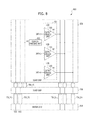
- FIG. 8 is a circuit diagram illustrating a multi-chip package in accordance with another embodiment of the present invention.
- a multi-chip package 800 includes a master chip 810 and a plurality of slave chips 820 and 830 .
- the master chip 810 is commonly coupled to the plurality of slave chips 820 and 830 through a through-chip-via, for example, a through-silicon-via, (TSV).
- TSV through-silicon-via
- FIG. 8 the TSV for transferring a power and data is shown in FIG. 8 . That is, a power TSV TSV_P 1 and TSV_P 2 for supplying a power supply voltage VDD and a ground voltage VSS, and a data TSV TSV_D 1 and TSV_Dn for transferring first to n th data are shown in FIG. 8 .
- a charge TSV TSV_P 3 for receiving and transferring a recovery power driving voltage VM.
- the master chip 810 controls a plurality of slave chips 820 .
- the plurality of slave chips 820 perform various operations based on a control of the master chip 810 .
- one of the plurality of slave chips 820 will be described.
- the slave chip 820 includes first to n th output driving units 821 , and a common charging unit 822 .
- the first to n th output driving units 821 receive the power supply voltage VDD, the ground voltage VSS and the recovery power driving voltage VM, and drives first to n th data TSVs TSV_D 1 , . . . , TSV_Dn corresponding to first to n th data DAT ⁇ 1:n> to be outputted.
- the first to n th output driving units 821 receive the power supply voltage VDD, the ground voltage VSS and the recovery power driving voltage VM. This represents that output data of the first to n th output driving units 821 may have three levels.
- the common charging unit 822 is charged by charges remained on the first to n th data TSVs TSV_D 1 , . . . , TSV_Dn.
- the stored charges have the recovery power driving voltage VM, and are supplied to the first to n th output driving units 821 through the charge TSV TSV_P 3 .
- the multi-chip package in accordance with an embodiment of the present invention may be charged by the charges remained on a plurality of data TSVs TSV_D 1 , . . . , TSV_Dn and transfer the stored charges to the plurality of slave chips 820 and 830 through the charge TSV TSV_P 3 .
- the charge TSV TSV_P 3 shown in FIG. 8 is coupled to the plurality of slave chips 820 and 830 .
- the charge TSV TSV_P 3 may be coupled to the master chip 810 .
- the charges used in a data transmission operation may be reused in embodiments of the present invention.
- a power consumption of the data transmission operation may be efficiently controlled by the reusing operation of the charge.
- a high speed operation may be implemented without increasing a number of data transmission lines, for example, TSVs, and raising an operation frequency.
- the data output circuit in accordance with embodiments of the present invention minimizes a power consumption of data transmission operation by reusing an energy, which is used for transferring data, during a data transmission operation.
- a location and a kind of a logic gate and a transistor which are exemplarily described in embodiments of the present invention, may be differently designed according to a polarity of an input signal.
Landscapes
- Engineering & Computer Science (AREA)
- Computer Hardware Design (AREA)
- Physics & Mathematics (AREA)
- Computing Systems (AREA)
- General Engineering & Computer Science (AREA)
- Mathematical Physics (AREA)
- Power Engineering (AREA)
- Logic Circuits (AREA)
- Dram (AREA)
- Dc Digital Transmission (AREA)
- Charge And Discharge Circuits For Batteries Or The Like (AREA)
Applications Claiming Priority (2)
| Application Number | Priority Date | Filing Date | Title |
|---|---|---|---|
| KR1020130040057A KR102048254B1 (ko) | 2013-04-11 | 2013-04-11 | 데이터 출력 회로 및 그의 구동 방법 |
| KR10-2013-0040057 | 2013-04-11 |
Publications (2)
| Publication Number | Publication Date |
|---|---|
| US20140306734A1 US20140306734A1 (en) | 2014-10-16 |
| US9917585B2 true US9917585B2 (en) | 2018-03-13 |
Family
ID=51671378
Family Applications (1)
| Application Number | Title | Priority Date | Filing Date |
|---|---|---|---|
| US13/935,931 Active 2036-02-18 US9917585B2 (en) | 2013-04-11 | 2013-07-05 | Data output circuit and method for driving the same |
Country Status (4)
| Country | Link |
|---|---|
| US (1) | US9917585B2 (ko) |
| KR (1) | KR102048254B1 (ko) |
| CN (1) | CN104103307B (ko) |
| TW (1) | TWI611416B (ko) |
Cited By (1)
| Publication number | Priority date | Publication date | Assignee | Title |
|---|---|---|---|---|
| US20200052701A1 (en) * | 2018-08-13 | 2020-02-13 | Shenzhen GOODIX Technology Co., Ltd. | Data interface, chip, and chip system |
Families Citing this family (6)
| Publication number | Priority date | Publication date | Assignee | Title |
|---|---|---|---|---|
| KR20160043714A (ko) * | 2014-10-14 | 2016-04-22 | 에스케이하이닉스 주식회사 | 관통 비아를 갖는 반도체 메모리 장치 |
| KR20160121224A (ko) * | 2015-04-10 | 2016-10-19 | 에스케이하이닉스 주식회사 | 고속 통신을 위한 전송장치, 이를 포함하는 인터페이스 회로 및 시스템 |
| US9378778B1 (en) | 2015-06-14 | 2016-06-28 | Darryl G. Walker | Package including a plurality of stacked semiconductor devices including a capacitance enhanced through via and method of manufacture |
| KR20190001300A (ko) * | 2017-06-27 | 2019-01-04 | 에스케이하이닉스 주식회사 | 컨트롤러 및 메모리 시스템 및 메모리 시스템의 동작 방법 |
| US10896723B2 (en) * | 2019-04-30 | 2021-01-19 | Ambient Scientific Inc. | Signal communication circuit implementing receiver and transmitter circuits |
| CN115347894B (zh) * | 2022-10-17 | 2023-02-10 | 杭州岸达科技有限公司 | 一种射频接口电路及基于射频接口电路的多芯片级联方法 |
Citations (25)
| Publication number | Priority date | Publication date | Assignee | Title |
|---|---|---|---|---|
| US5565796A (en) * | 1995-05-24 | 1996-10-15 | Mitsubishi Denki Kabushiki Kaisha | Bus drive circuit, receiver circuit, and bus system |
| KR20010060834A (ko) | 1999-12-28 | 2001-07-07 | 박종섭 | 박막트랜지스터 액정표시 장치의2레벨 전압 공유 방법 및그 회로 |
| US6307417B1 (en) * | 1999-08-24 | 2001-10-23 | Robert J. Proebsting | Integrated circuit output buffers having reduced power consumption requirements and methods of operating same |
| US6404237B1 (en) * | 2000-12-29 | 2002-06-11 | Intel Corporation | Boosted multiplexer transmission gate |
| US20020089382A1 (en) * | 2001-01-06 | 2002-07-11 | Samsung Electronics Co., Ltd. | Charge pump circuit for improving switching characteristics and reducing leakage current and phase locked loop having the same |
| US20020175749A1 (en) * | 2001-05-11 | 2002-11-28 | Hedberg Mats Olof Joakim | Differential signal transfer circuit |
| US6707324B1 (en) * | 2002-11-20 | 2004-03-16 | Via Technologies, Inc. | Low ground bounce output driver |
| US6717440B2 (en) * | 2001-01-22 | 2004-04-06 | Micron Technology, Inc. | System and method for improving signal propagation |
| US20040119520A1 (en) * | 2002-12-21 | 2004-06-24 | Bae Seung Cheol | Setup/hold time control device |
| US7130225B1 (en) * | 2004-03-03 | 2006-10-31 | Atheros Communications, Inc. | Charge pump with large bypass capacitors |
| US20070024328A1 (en) * | 2005-08-01 | 2007-02-01 | Shin Soon-Kyun | Output driver with maintained slew rate |
| US20080136487A1 (en) * | 2006-12-06 | 2008-06-12 | Princeton Technology Corporation | Boost circuit and level shifter |
| US7420395B2 (en) * | 2006-03-29 | 2008-09-02 | Kawasaki Microelectronics, Inc. | Output buffer circuit and system including the output buffer circuit |
| US20100052728A1 (en) * | 2008-08-28 | 2010-03-04 | Wei Ye Lu | Load sense and active noise reduction for i/o circuit |
| US7728619B1 (en) * | 2007-03-30 | 2010-06-01 | Cypress Semiconductor Corporation | Circuit and method for cascading programmable impedance matching in a multi-chip system |
| US20110025380A1 (en) * | 2009-07-29 | 2011-02-03 | Samsung Electronics Co., Ltd. | Output driver operable over wide range of voltages |
| US20110272788A1 (en) * | 2010-05-10 | 2011-11-10 | International Business Machines Corporation | Computer system wafer integrating different dies in stacked master-slave structures |
| KR20110138099A (ko) | 2010-06-18 | 2011-12-26 | 삼성전자주식회사 | 관통 전극을 갖는 3차원 적층 구조의 반도체 장치 및 그 반도체 장치의 시그널링 방법 |
| US8310855B2 (en) * | 2009-07-29 | 2012-11-13 | Elpida Memory, Inc. | Semiconductor device |
| US8559258B1 (en) * | 2011-12-13 | 2013-10-15 | Michael C. Stephens, Jr. | Self-refresh adjustment in memory devices configured for stacked arrangements |
| US8611437B2 (en) * | 2012-01-26 | 2013-12-17 | Nvidia Corporation | Ground referenced single-ended signaling |
| US8766678B2 (en) * | 2009-09-30 | 2014-07-01 | SK Hynix Inc. | Semiconductor apparatus and method for controlling the same |
| US9170287B2 (en) * | 2012-02-21 | 2015-10-27 | National Tsing Hua University | 3D-IC differential sensing and charge sharing scheme |
| US9263371B2 (en) * | 2014-01-17 | 2016-02-16 | Sk Hynix | Semiconductor device having through-silicon via |
| US9275984B2 (en) * | 2013-04-11 | 2016-03-01 | SK Hynix Inc. | Multi-chip package system |
Family Cites Families (3)
| Publication number | Priority date | Publication date | Assignee | Title |
|---|---|---|---|---|
| US20080137401A1 (en) * | 2006-12-07 | 2008-06-12 | Jan Boris Philipp | Memory that limits power consumption |
| KR101625380B1 (ko) * | 2009-11-16 | 2016-06-14 | 삼성전자주식회사 | 전하 재활용 메모리 시스템 및 그것의 전하 재활용 방법 |
| KR101175249B1 (ko) * | 2011-04-27 | 2012-08-21 | 에스케이하이닉스 주식회사 | 반도체 메모리 장치 및 그 동작방법 |
-
2013
- 2013-04-11 KR KR1020130040057A patent/KR102048254B1/ko active IP Right Grant
- 2013-07-05 US US13/935,931 patent/US9917585B2/en active Active
- 2013-09-05 TW TW102132064A patent/TWI611416B/zh active
- 2013-11-22 CN CN201310597099.3A patent/CN104103307B/zh active Active
Patent Citations (26)
| Publication number | Priority date | Publication date | Assignee | Title |
|---|---|---|---|---|
| US5565796A (en) * | 1995-05-24 | 1996-10-15 | Mitsubishi Denki Kabushiki Kaisha | Bus drive circuit, receiver circuit, and bus system |
| US6307417B1 (en) * | 1999-08-24 | 2001-10-23 | Robert J. Proebsting | Integrated circuit output buffers having reduced power consumption requirements and methods of operating same |
| KR20010060834A (ko) | 1999-12-28 | 2001-07-07 | 박종섭 | 박막트랜지스터 액정표시 장치의2레벨 전압 공유 방법 및그 회로 |
| US6404237B1 (en) * | 2000-12-29 | 2002-06-11 | Intel Corporation | Boosted multiplexer transmission gate |
| US20020084803A1 (en) * | 2000-12-29 | 2002-07-04 | Mathew Sanu K. | Boosted multiplexer transmission gate |
| US20020089382A1 (en) * | 2001-01-06 | 2002-07-11 | Samsung Electronics Co., Ltd. | Charge pump circuit for improving switching characteristics and reducing leakage current and phase locked loop having the same |
| US6717440B2 (en) * | 2001-01-22 | 2004-04-06 | Micron Technology, Inc. | System and method for improving signal propagation |
| US20020175749A1 (en) * | 2001-05-11 | 2002-11-28 | Hedberg Mats Olof Joakim | Differential signal transfer circuit |
| US6707324B1 (en) * | 2002-11-20 | 2004-03-16 | Via Technologies, Inc. | Low ground bounce output driver |
| US20040119520A1 (en) * | 2002-12-21 | 2004-06-24 | Bae Seung Cheol | Setup/hold time control device |
| US7130225B1 (en) * | 2004-03-03 | 2006-10-31 | Atheros Communications, Inc. | Charge pump with large bypass capacitors |
| US20070024328A1 (en) * | 2005-08-01 | 2007-02-01 | Shin Soon-Kyun | Output driver with maintained slew rate |
| US7420395B2 (en) * | 2006-03-29 | 2008-09-02 | Kawasaki Microelectronics, Inc. | Output buffer circuit and system including the output buffer circuit |
| US20080136487A1 (en) * | 2006-12-06 | 2008-06-12 | Princeton Technology Corporation | Boost circuit and level shifter |
| US7728619B1 (en) * | 2007-03-30 | 2010-06-01 | Cypress Semiconductor Corporation | Circuit and method for cascading programmable impedance matching in a multi-chip system |
| US20100052728A1 (en) * | 2008-08-28 | 2010-03-04 | Wei Ye Lu | Load sense and active noise reduction for i/o circuit |
| US20110025380A1 (en) * | 2009-07-29 | 2011-02-03 | Samsung Electronics Co., Ltd. | Output driver operable over wide range of voltages |
| US8310855B2 (en) * | 2009-07-29 | 2012-11-13 | Elpida Memory, Inc. | Semiconductor device |
| US8766678B2 (en) * | 2009-09-30 | 2014-07-01 | SK Hynix Inc. | Semiconductor apparatus and method for controlling the same |
| US20110272788A1 (en) * | 2010-05-10 | 2011-11-10 | International Business Machines Corporation | Computer system wafer integrating different dies in stacked master-slave structures |
| KR20110138099A (ko) | 2010-06-18 | 2011-12-26 | 삼성전자주식회사 | 관통 전극을 갖는 3차원 적층 구조의 반도체 장치 및 그 반도체 장치의 시그널링 방법 |
| US8559258B1 (en) * | 2011-12-13 | 2013-10-15 | Michael C. Stephens, Jr. | Self-refresh adjustment in memory devices configured for stacked arrangements |
| US8611437B2 (en) * | 2012-01-26 | 2013-12-17 | Nvidia Corporation | Ground referenced single-ended signaling |
| US9170287B2 (en) * | 2012-02-21 | 2015-10-27 | National Tsing Hua University | 3D-IC differential sensing and charge sharing scheme |
| US9275984B2 (en) * | 2013-04-11 | 2016-03-01 | SK Hynix Inc. | Multi-chip package system |
| US9263371B2 (en) * | 2014-01-17 | 2016-02-16 | Sk Hynix | Semiconductor device having through-silicon via |
Cited By (2)
| Publication number | Priority date | Publication date | Assignee | Title |
|---|---|---|---|---|
| US20200052701A1 (en) * | 2018-08-13 | 2020-02-13 | Shenzhen GOODIX Technology Co., Ltd. | Data interface, chip, and chip system |
| US10855279B2 (en) * | 2018-08-13 | 2020-12-01 | Shenzhen GOODIX Technology Co., Ltd. | Data interface, chip, and chip system |
Also Published As
| Publication number | Publication date |
|---|---|
| CN104103307A (zh) | 2014-10-15 |
| TWI611416B (zh) | 2018-01-11 |
| KR102048254B1 (ko) | 2020-01-08 |
| US20140306734A1 (en) | 2014-10-16 |
| KR20140122949A (ko) | 2014-10-21 |
| CN104103307B (zh) | 2019-02-01 |
| TW201440070A (zh) | 2014-10-16 |
Similar Documents
| Publication | Publication Date | Title |
|---|---|---|
| US9917585B2 (en) | Data output circuit and method for driving the same | |
| US9013951B2 (en) | Word line drivers and semiconductor memory devices including the same | |
| US9455002B2 (en) | Amplifying circuit and semiconductor memory device including the same | |
| US11651816B2 (en) | Memory unit | |
| US7940074B2 (en) | Data transmission circuit and semiconductor apparatus including the same | |
| US8750014B2 (en) | Tri-state driver circuits having automatic high-impedance enabling | |
| US20180144789A1 (en) | Semiconductor device, semiconductor system including the same and read and write operation method thereof | |
| US8411478B2 (en) | Three-dimensional stacked semiconductor integrated circuit | |
| KR20080083796A (ko) | 반도체 메모리 시스템 | |
| US8300481B2 (en) | Apparatus and method for transmitting/receiving signals at high speed | |
| JP2009071798A (ja) | 集積回路装置のデータバス電荷共有技術 | |
| US10083723B1 (en) | Apparatuses and methods for sharing transmission vias for memory devices | |
| US9305621B2 (en) | Semiconductor devices and semiconductor systems including the same | |
| US7764557B2 (en) | Sense amplifier driving circuit and semiconductor device having the same | |
| US8913452B2 (en) | Semiconductor device and semiconductor memory device | |
| US9379701B2 (en) | Semiconductor device having through chip via | |
| US9418725B2 (en) | Semiconductor device and method of driving the same | |
| US20080225610A1 (en) | Write driver of semiconductor memory device and driving method thereof | |
| US11380370B2 (en) | Semiconductor device having a charge pump | |
| US8390338B2 (en) | Semiconductor device having signal transfer line | |
| US8050120B2 (en) | Sensing delay circuit and semiconductor memory device using the same | |
| US7969800B2 (en) | Semiconductor memory apparatus | |
| KR20110072549A (ko) | 반도체 장치 | |
| KR100857875B1 (ko) | 반도체 소자의 라이트 드라이버 | |
| KR20090024498A (ko) | 고속의 신호 송수신 장치 및 방법 |
Legal Events
| Date | Code | Title | Description |
|---|---|---|---|
| AS | Assignment |
Owner name: SK HYNIX INC., KOREA, REPUBLIC OF Free format text: ASSIGNMENT OF ASSIGNORS INTEREST;ASSIGNOR:LEE, DONG-UK;REEL/FRAME:030743/0649 Effective date: 20130701 |
|
| STCF | Information on status: patent grant |
Free format text: PATENTED CASE |
|
| MAFP | Maintenance fee payment |
Free format text: PAYMENT OF MAINTENANCE FEE, 4TH YEAR, LARGE ENTITY (ORIGINAL EVENT CODE: M1551); ENTITY STATUS OF PATENT OWNER: LARGE ENTITY Year of fee payment: 4 |