US9815138B2 - Wafer producing method - Google Patents
Wafer producing method Download PDFInfo
- Publication number
- US9815138B2 US9815138B2 US15/165,686 US201615165686A US9815138B2 US 9815138 B2 US9815138 B2 US 9815138B2 US 201615165686 A US201615165686 A US 201615165686A US 9815138 B2 US9815138 B2 US 9815138B2
- Authority
- US
- United States
- Prior art keywords
- wafer
- ingot
- single crystal
- laser beam
- modified layer
- Prior art date
- Legal status (The legal status is an assumption and is not a legal conclusion. Google has not performed a legal analysis and makes no representation as to the accuracy of the status listed.)
- Active, expires
Links
- 238000000034 method Methods 0.000 title claims description 20
- 239000013078 crystal Substances 0.000 claims abstract description 33
- 238000000926 separation method Methods 0.000 claims abstract description 29
- 238000004519 manufacturing process Methods 0.000 claims abstract description 4
- 230000005540 biological transmission Effects 0.000 claims description 4
- 230000015572 biosynthetic process Effects 0.000 abstract description 4
- 239000010410 layer Substances 0.000 description 43
- 235000012431 wafers Nutrition 0.000 description 40
- 230000007246 mechanism Effects 0.000 description 12
- 238000003825 pressing Methods 0.000 description 9
- 238000005520 cutting process Methods 0.000 description 5
- 239000002346 layers by function Substances 0.000 description 4
- 230000001902 propagating effect Effects 0.000 description 4
- 230000003287 optical effect Effects 0.000 description 3
- 238000000638 solvent extraction Methods 0.000 description 2
- 229910009372 YVO4 Inorganic materials 0.000 description 1
- 239000000853 adhesive Substances 0.000 description 1
- 230000001070 adhesive effect Effects 0.000 description 1
- 238000010586 diagram Methods 0.000 description 1
- 238000003384 imaging method Methods 0.000 description 1
- 230000006872 improvement Effects 0.000 description 1
- 238000012986 modification Methods 0.000 description 1
- 230000004048 modification Effects 0.000 description 1
- 230000009467 reduction Effects 0.000 description 1
- 229910052710 silicon Inorganic materials 0.000 description 1
- 239000010703 silicon Substances 0.000 description 1
Images


Classifications
-
- H—ELECTRICITY
- H01—ELECTRIC ELEMENTS
- H01L—SEMICONDUCTOR DEVICES NOT COVERED BY CLASS H10
- H01L21/00—Processes or apparatus adapted for the manufacture or treatment of semiconductor or solid state devices or of parts thereof
- H01L21/70—Manufacture or treatment of devices consisting of a plurality of solid state components formed in or on a common substrate or of parts thereof; Manufacture of integrated circuit devices or of parts thereof
- H01L21/77—Manufacture or treatment of devices consisting of a plurality of solid state components or integrated circuits formed in, or on, a common substrate
- H01L21/78—Manufacture or treatment of devices consisting of a plurality of solid state components or integrated circuits formed in, or on, a common substrate with subsequent division of the substrate into plural individual devices
-
- B—PERFORMING OPERATIONS; TRANSPORTING
- B23—MACHINE TOOLS; METAL-WORKING NOT OTHERWISE PROVIDED FOR
- B23K—SOLDERING OR UNSOLDERING; WELDING; CLADDING OR PLATING BY SOLDERING OR WELDING; CUTTING BY APPLYING HEAT LOCALLY, e.g. FLAME CUTTING; WORKING BY LASER BEAM
- B23K26/00—Working by laser beam, e.g. welding, cutting or boring
- B23K26/02—Positioning or observing the workpiece, e.g. with respect to the point of impact; Aligning, aiming or focusing the laser beam
- B23K26/06—Shaping the laser beam, e.g. by masks or multi-focusing
- B23K26/0604—Shaping the laser beam, e.g. by masks or multi-focusing by a combination of beams
-
- B23K26/0057—
-
- B—PERFORMING OPERATIONS; TRANSPORTING
- B23—MACHINE TOOLS; METAL-WORKING NOT OTHERWISE PROVIDED FOR
- B23K—SOLDERING OR UNSOLDERING; WELDING; CLADDING OR PLATING BY SOLDERING OR WELDING; CUTTING BY APPLYING HEAT LOCALLY, e.g. FLAME CUTTING; WORKING BY LASER BEAM
- B23K26/00—Working by laser beam, e.g. welding, cutting or boring
- B23K26/08—Devices involving relative movement between laser beam and workpiece
- B23K26/0869—Devices involving movement of the laser head in at least one axial direction
- B23K26/0876—Devices involving movement of the laser head in at least one axial direction in at least two axial directions
-
- B—PERFORMING OPERATIONS; TRANSPORTING
- B23—MACHINE TOOLS; METAL-WORKING NOT OTHERWISE PROVIDED FOR
- B23K—SOLDERING OR UNSOLDERING; WELDING; CLADDING OR PLATING BY SOLDERING OR WELDING; CUTTING BY APPLYING HEAT LOCALLY, e.g. FLAME CUTTING; WORKING BY LASER BEAM
- B23K26/00—Working by laser beam, e.g. welding, cutting or boring
- B23K26/50—Working by transmitting the laser beam through or within the workpiece
- B23K26/53—Working by transmitting the laser beam through or within the workpiece for modifying or reforming the material inside the workpiece, e.g. for producing break initiation cracks
-
- H—ELECTRICITY
- H01—ELECTRIC ELEMENTS
- H01L—SEMICONDUCTOR DEVICES NOT COVERED BY CLASS H10
- H01L21/00—Processes or apparatus adapted for the manufacture or treatment of semiconductor or solid state devices or of parts thereof
- H01L21/02—Manufacture or treatment of semiconductor devices or of parts thereof
- H01L21/02002—Preparing wafers
-
- H—ELECTRICITY
- H01—ELECTRIC ELEMENTS
- H01L—SEMICONDUCTOR DEVICES NOT COVERED BY CLASS H10
- H01L21/00—Processes or apparatus adapted for the manufacture or treatment of semiconductor or solid state devices or of parts thereof
- H01L21/02—Manufacture or treatment of semiconductor devices or of parts thereof
- H01L21/02104—Forming layers
- H01L21/02365—Forming inorganic semiconducting materials on a substrate
- H01L21/02518—Deposited layers
- H01L21/02587—Structure
- H01L21/0259—Microstructure
- H01L21/02598—Microstructure monocrystalline
-
- H—ELECTRICITY
- H01—ELECTRIC ELEMENTS
- H01L—SEMICONDUCTOR DEVICES NOT COVERED BY CLASS H10
- H01L21/00—Processes or apparatus adapted for the manufacture or treatment of semiconductor or solid state devices or of parts thereof
- H01L21/02—Manufacture or treatment of semiconductor devices or of parts thereof
- H01L21/04—Manufacture or treatment of semiconductor devices or of parts thereof the devices having at least one potential-jump barrier or surface barrier, e.g. PN junction, depletion layer or carrier concentration layer
- H01L21/18—Manufacture or treatment of semiconductor devices or of parts thereof the devices having at least one potential-jump barrier or surface barrier, e.g. PN junction, depletion layer or carrier concentration layer the devices having semiconductor bodies comprising elements of Group IV of the Periodic System or AIIIBV compounds with or without impurities, e.g. doping materials
- H01L21/26—Bombardment with radiation
- H01L21/263—Bombardment with radiation with high-energy radiation
- H01L21/268—Bombardment with radiation with high-energy radiation using electromagnetic radiation, e.g. laser radiation
-
- H—ELECTRICITY
- H01—ELECTRIC ELEMENTS
- H01L—SEMICONDUCTOR DEVICES NOT COVERED BY CLASS H10
- H01L21/00—Processes or apparatus adapted for the manufacture or treatment of semiconductor or solid state devices or of parts thereof
- H01L21/70—Manufacture or treatment of devices consisting of a plurality of solid state components formed in or on a common substrate or of parts thereof; Manufacture of integrated circuit devices or of parts thereof
- H01L21/71—Manufacture of specific parts of devices defined in group H01L21/70
- H01L21/76—Making of isolation regions between components
-
- H—ELECTRICITY
- H01—ELECTRIC ELEMENTS
- H01L—SEMICONDUCTOR DEVICES NOT COVERED BY CLASS H10
- H01L29/00—Semiconductor devices adapted for rectifying, amplifying, oscillating or switching, or capacitors or resistors with at least one potential-jump barrier or surface barrier, e.g. PN junction depletion layer or carrier concentration layer; Details of semiconductor bodies or of electrodes thereof ; Multistep manufacturing processes therefor
- H01L29/02—Semiconductor bodies ; Multistep manufacturing processes therefor
- H01L29/04—Semiconductor bodies ; Multistep manufacturing processes therefor characterised by their crystalline structure, e.g. polycrystalline, cubic or particular orientation of crystalline planes
-
- H—ELECTRICITY
- H01—ELECTRIC ELEMENTS
- H01L—SEMICONDUCTOR DEVICES NOT COVERED BY CLASS H10
- H01L29/00—Semiconductor devices adapted for rectifying, amplifying, oscillating or switching, or capacitors or resistors with at least one potential-jump barrier or surface barrier, e.g. PN junction depletion layer or carrier concentration layer; Details of semiconductor bodies or of electrodes thereof ; Multistep manufacturing processes therefor
- H01L29/02—Semiconductor bodies ; Multistep manufacturing processes therefor
- H01L29/12—Semiconductor bodies ; Multistep manufacturing processes therefor characterised by the materials of which they are formed
- H01L29/16—Semiconductor bodies ; Multistep manufacturing processes therefor characterised by the materials of which they are formed including, apart from doping materials or other impurities, only elements of Group IV of the Periodic System
- H01L29/1608—Silicon carbide
-
- H—ELECTRICITY
- H01—ELECTRIC ELEMENTS
- H01L—SEMICONDUCTOR DEVICES NOT COVERED BY CLASS H10
- H01L29/00—Semiconductor devices adapted for rectifying, amplifying, oscillating or switching, or capacitors or resistors with at least one potential-jump barrier or surface barrier, e.g. PN junction depletion layer or carrier concentration layer; Details of semiconductor bodies or of electrodes thereof ; Multistep manufacturing processes therefor
- H01L29/02—Semiconductor bodies ; Multistep manufacturing processes therefor
- H01L29/12—Semiconductor bodies ; Multistep manufacturing processes therefor characterised by the materials of which they are formed
- H01L29/20—Semiconductor bodies ; Multistep manufacturing processes therefor characterised by the materials of which they are formed including, apart from doping materials or other impurities, only AIIIBV compounds
- H01L29/2003—Nitride compounds
-
- B—PERFORMING OPERATIONS; TRANSPORTING
- B23—MACHINE TOOLS; METAL-WORKING NOT OTHERWISE PROVIDED FOR
- B23K—SOLDERING OR UNSOLDERING; WELDING; CLADDING OR PLATING BY SOLDERING OR WELDING; CUTTING BY APPLYING HEAT LOCALLY, e.g. FLAME CUTTING; WORKING BY LASER BEAM
- B23K2103/00—Materials to be soldered, welded or cut
- B23K2103/50—Inorganic material, e.g. metals, not provided for in B23K2103/02 – B23K2103/26
- B23K2103/56—Inorganic material, e.g. metals, not provided for in B23K2103/02 – B23K2103/26 semiconducting
-
- B23K2203/56—
Definitions
- the present invention relates to a wafer producing method for slicing a hexagonal single crystal ingot to produce a wafer.
- Various devices such as ICs and LSIs are formed by forming a functional layer on the front side of a wafer formed of silicon or the like and partitioning this functional layer into a plurality of regions along a plurality of crossing division lines.
- the division lines of the wafer are processed by a processing apparatus such as a cutting apparatus and a laser processing apparatus to thereby divide the wafer into a plurality of individual device chips corresponding to the devices.
- the device chips thus obtained are widely used in various electronic apparatuses such as mobile phones and personal computers.
- power devices or optical devices such as LEDs and LDs are formed by forming a functional layer on the front side of a wafer formed of a hexagonal single crystal such as SiC and GaN and partitioning this functional layer into a plurality of regions along a plurality of crossing division lines.
- the wafer on which the devices are to be formed is produced by slicing an ingot with a wire saw. Both sides of the wafer obtained above are polished to a mirror finish (see Japanese Patent Laid-Open No. 2000-94221, for example).
- This wire saw is configured in such a manner that a single wire such as a piano wire having a diameter of approximately 100 to 300 ⁇ m is wound around many grooves formed on usually two to four guide rollers to form a plurality of cutting portions spaced in parallel with a given pitch.
- the wire is operated to run in one direction or opposite directions, thereby slicing the ingot into a plurality of wafers.
- This technique includes the steps of setting the focal point of a laser beam having a transmission wavelength to SiC inside a hexagonal single crystal ingot, next applying the laser beam to the ingot as scanning the laser beam on the ingot to thereby form a modified layer and cracks in a separation plane inside the ingot, and next applying an external force to the ingot to thereby break the ingot along the separation plane where the modified layer and the cracks are formed, thus separating a wafer from the ingot.
- the laser beam (pulsed laser beam) is scanned spirally or linearly along the separation plane so that a first application point of the laser beam and a second application point of the laser beam nearest to the first application point have a predetermined positional relation with each other.
- the modified layer and the cracks are formed at very high density in the separation plane of the ingot.
- the laser beam is scanned spirally or linearly on the ingot.
- the direction of scanning of the laser beam is not specified.
- the pitch (spacing) between the first application point and the second application point of the laser beam as mentioned above is set to 1 ⁇ m to 10 ⁇ m. This pitch corresponds to the pitch of the cracks extending from the modified layer along a c-plane defined in the ingot.
- the pitch of the application points of the laser beam to be applied to the ingot is very small. Accordingly, regardless of whether the laser beam is scanned spirally or linearly, the laser beam must be applied with a very small pitch and the improvement in productivity is not yet sufficient.
- a wafer producing method for producing a hexagonal single crystal wafer from a hexagonal single crystal ingot having a first surface, a second surface opposite to the first surface, a c-axis extending from the first surface to the second surface, and a c-plane perpendicular to the c-axis, the wafer producing method including a separation start point forming step of setting the focal point of a laser beam having a transmission wavelength to the ingot inside the ingot at a predetermined depth from the first surface, which depth corresponds to the thickness of the wafer to be produced, and next applying the laser beam to the first surface as relatively moving the focal point and the ingot to thereby form a modified layer parallel to the first surface and cracks extending from the modified layer along the c-plane, thus forming a separation start point; and a wafer separating step of separating plate-shaped member having a thickness corresponding to the thickness of the wafer from the ingot at the separation start point after performing the
- the predetermined spacing between any adjacent ones of the focal points is set so that the upper limit of the predetermined spacing becomes nearly equal to a spacing defined when the front ends of the cracks extending from the adjacent modified layers in the second direction overlap each other.
- the focal point of the laser beam is relatively moved in the first direction perpendicular to the second direction where the off angle is formed between the first surface and the c-plane of the ingot, thereby linearly forming the modified layer extending in the first direction.
- the focal point of the laser beam is indexed in the second direction by the predetermined amount.
- the focal point of the laser beam is relatively moved again in the first direction to thereby linearly form the modified layer extending in the first direction.
- Such a series of steps are repeated to form a plurality of modified layers extending in the first direction, wherein each modified layer is formed at the predetermined depth from the first surface of the ingot and the cracks are formed on both sides of each modified layer so as to propagate along the c-plane. Accordingly, any adjacent ones of the plural modified layers are connected together through the cracks formed therebetween, so that the plate-shaped member having the thickness corresponding to the thickness of the wafer can be easily separated from the ingot at the separation start point, thus producing the hexagonal single crystal wafer from the ingot.
- the plural laser beams are simultaneously applied to form the plural linear modified layers parallel to each other in the condition where the cracks formed between the adjacent modified layers are connected together.
- the separation start point can be efficiently formed to thereby sufficiently improve the productivity.
- the amount of the ingot to be discarded can be sufficiently reduced.
- FIG. 1 is a perspective view of a laser processing apparatus suitable for use in performing the wafer producing method of the present invention
- FIG. 2 is a block diagram of a laser beam generating unit
- FIG. 3 is a schematic view of a blazed diffractive optical element (DOE);
- FIG. 4A is a perspective view of a hexagonal single crystal ingot
- FIG. 4B is an elevational view of the ingot shown in FIG. 4A ;
- FIG. 5 is a perspective view for illustrating a separation start point forming step
- FIG. 6 is a plan view of the ingot shown in FIG. 4 A;
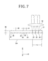
- FIG. 7 is a schematic sectional view for illustrating a modified layer forming step
- FIG. 8 is a schematic plan view for illustrating the modified layer forming step
- FIG. 9 is a schematic plan view for illustrating an indexing step
- FIGS. 10A and 10B are perspective views for illustrating a wafer separating step
- FIG. 11 is a perspective view of a hexagonal single crystal wafer produced from the ingot.
- FIG. 1 there is shown a perspective view of a laser processing apparatus 2 suitable for use in performing the wafer producing method of the present invention.
- the laser processing apparatus 2 includes a stationary base 4 and a first slide block 6 mounted on the stationary base 4 so as to be movable in the X direction.
- the first slide block 6 is moved in a feeding direction, or in the X direction along a pair of guide rails 14 by a feeding mechanism 12 including a ball screw 8 and a pulse motor 10 .
- a second slide block 16 is mounted on the first slide block 6 so as to be movable in the Y direction.
- the second slide block 16 is moved in an indexing direction, or in the Y direction along a pair of guide rails 24 by an indexing mechanism 22 including a ball screw 18 and a pulse motor 20 .
- a support table 26 is mounted on the second slide block 16 .
- the support table 26 is movable in the X direction and the Y direction by the feeding mechanism 12 and the indexing mechanism 22 and also rotatable by a motor stored in the second slide block 16 .
- a column 28 is provided on the stationary base 4 so as to project upward therefrom.
- a laser beam applying mechanism (laser beam applying means) 30 is mounted on the column 28 .
- the laser beam applying mechanism 30 includes a casing 32 , a laser beam generating unit 34 (see FIG. 2 ) stored in the casing 32 , and focusing means (laser head) 36 mounted on the front end of the casing 32 .
- An imaging unit 38 having a microscope and a camera is also mounted on the front end of the casing 32 so as to be aligned with the focusing means 36 in the X direction.
- the laser beam generating unit 34 includes a laser oscillator 40 such as YAG laser and YVO4 laser for generating a pulsed laser beam, repetition frequency setting means 42 for setting the repetition frequency of the pulsed laser beam to be generated by the laser oscillator 40 , pulse width adjusting means 44 for adjusting the pulse width of the pulsed laser beam to be generated by the laser oscillator 40 , and power adjusting means 46 for adjusting the power of the pulsed laser beam generated by the laser oscillator 40 .
- the laser oscillator 40 has a Brewster window, so that the laser beam generated from the laser oscillator 40 is a laser beam of linearly polarized light.
- the pulsed laser beam is reflected by a mirror 48 included in the focusing means 36 and next branched into three laser beams by a diffractive optical element (DOE) 50 included in the focusing means 36 .
- DOE diffractive optical element
- These three laser beams obtained by the DOE 50 are next focused by a focusing lens 51 included in the focusing means 36 .
- the focusing lens 51 is positioned so that the pulsed laser beam is focused inside a hexagonal single crystal ingot 11 as a workpiece fixed to the support table 26 .
- the DOE 50 is provided by a blazed DOE as shown in FIG. 3 .
- the blazed DOE 50 includes a transparent plate 62 and a sawtooth sectional structure 64 finely formed on one side (upper surface as viewed in FIG. 3 ) of the transparent plate 62 .
- the size d 1 of each sawtooth in the structure 64 is set to several tens to several hundreds of micrometers.
- the laser beam as incident light to the blazed DOE 50 is branched into zeroth-order light, first-order light, and second-order light. The zeroth-order light, the first-order light, and the second-order light are next emerged as three separate laser beams from the blazed DOE 50 .
- FIG. 4A there is shown a perspective view of the hexagonal single crystal ingot 11 as a workpiece to be processed.
- FIG. 4B is an elevational view of the hexagonal single crystal ingot 11 shown in FIG. 4A .
- the hexagonal single crystal ingot (which will be hereinafter referred to also simply as ingot) 11 is selected from an SiC single crystal ingot and a GaN single crystal ingot.
- the ingot 11 has a first surface (upper surface) 11 a and a second surface (lower surface) 11 b opposite to the first surface 11 a .
- the first surface 11 a of the ingot 11 is preliminarily polished to a mirror finish because the laser beam is applied to the first surface 11 a.
- the ingot 11 has a first orientation flat 13 and a second orientation flat 15 perpendicular to the first orientation flat 13 .
- the length of the first orientation flat 13 is set longer than the length of the second orientation flat 15 .
- the ingot 11 has a c-axis 19 inclined by an off angle ⁇ toward the second orientation flat 15 with respect to a normal 17 to the upper surface 11 a and also has a c-plane 21 perpendicular to the c-axis 19 .
- the c-plane 21 is inclined by the off angle ⁇ with respect to the upper surface 11 a .
- the direction perpendicular to the direction of extension of the shorter second orientation flat 15 is the direction of inclination of the c-axis.
- the c-plane 21 is set in the ingot 11 innumerably at the molecular level of the ingot 11 .
- the off angle ⁇ is set to 4°.
- the off angle ⁇ is not limited to 4° in the present invention.
- the off angle ⁇ may be freely set in the range of 1° to 6° in manufacturing the ingot 11 .
- a column 52 is fixed to the left side of the stationary base 4 .
- the column 52 is formed with a vertically elongated opening 53 , and a pressing mechanism 54 is vertically movably mounted to the column 52 so as to project from the opening 53 .
- the ingot 11 is fixed to the upper surface of the support table 26 by using a wax or adhesive in the condition where the second orientation flat 15 of the ingot 11 becomes parallel to the X direction.
- the direction of formation of the off angle ⁇ is shown by an arrow Y 1 . That is, the direction of the arrow Y 1 is the direction where the intersection 19 a between the c-axis 19 and the upper surface 11 a of the ingot 11 is present with respect to the normal 17 to the upper surface 11 a .
- the direction perpendicular to the direction of the arrow Y 1 is shown by an arrow A. Then, the ingot 11 is fixed to the support table 26 in the condition where the direction of the arrow A becomes parallel to the X direction.
- the laser beam is scanned in the direction of the arrow A perpendicular to the direction of the arrow Y 1 , or the direction of formation of the off angle ⁇ .
- the direction of the arrow A perpendicular to the direction of the arrow Y 1 where the off angle ⁇ is formed is defined as the feeding direction of the support table 26 .
- the scanning direction of the laser beam to be applied from the focusing means 36 is set to the direction of the arrow A perpendicular to the direction of the arrow Y 1 where the off angle ⁇ of the ingot 11 is formed. That is, it was found that by setting the scanning direction of the laser beam to the direction of the arrow A as mentioned above in the wafer producing method of the present invention, cracks propagating from a modified layer formed inside the ingot 11 by the laser beam extend very long along the c-plane 21 .
- a separation start point forming step is performed in such a manner that the focal point of the laser beam having a transmission wavelength (e.g., 1064 nm) to the hexagonal single crystal ingot 11 fixed to the support table 26 is set inside the ingot 11 at a predetermined depth from the first surface (upper surface) 11 a , which depth corresponds to the thickness of a wafer to be produced, and the laser beam is next applied to the upper surface 11 a as relatively moving the focal point and the ingot 11 to thereby form a modified layer 23 parallel to the upper surface 11 a and cracks 25 propagating from the modified layer 23 along the c-plane 21 , thus forming a separation start point.
- a transmission wavelength e.g. 1064 nm
- This separation start point forming step includes a modified layer forming step of relatively moving the focal point of the laser beam in the direction of the arrow A perpendicular to the direction of the arrow Y 1 where the c-axis 19 is inclined by the off angle ⁇ with respect to the normal 17 to the upper surface 11 a and the off angle ⁇ is formed between the c-plane 21 and the upper surface 11 a , thereby forming the modified layer 23 inside the ingot 11 and the cracks 25 propagating from the modified layer 23 along the c-plane 21 , and also includes an indexing step of relatively moving the focal point in the direction of formation of the off angle ⁇ , i.e., in the Y direction to thereby index the focal point by a predetermined amount as shown in FIGS. 8 and 9 .
- the modified layer 23 is linearly formed so as to extend in the X direction, so that the cracks 25 propagate from the modified layer 23 in opposite directions along the c-plane 21 .
- the separation start point forming step further includes an index amount setting step of measuring the width of the cracks 25 formed on one side of the modified layer 23 along the c-plane 21 and then setting the index amount of the focal point according to the width mentioned above.
- the predetermined spacing H between any adjacent ones of the two or more focal points is set so that the upper limit of the spacing H becomes nearly equal to 2W1 defined when the front ends of the cracks 25 extending from the adjacent modified layers 23 in the Y direction overlap each other.
- M is the number of focal points.
- the separation start point forming step is performed under the following laser processing conditions.
- NA of the focusing lens 0.43
- the width W 1 of the cracks 25 propagating from the modified layer 23 along the c-plane 21 on one side as viewed in FIG. 7 is set to approximately 250 ⁇ m, and the index amount L is set to 1200 ⁇ m.
- the average power of the laser beam is not limited to 3.2 W.
- the width W 1 of the cracks 25 was approximately 100 ⁇ m.
- the width W 1 of the cracks 25 was approximately 350 ⁇ m.
- the average power of the laser beam to be applied is preferably set in the range of 2 W to 4.5 W.
- the average power of the laser beam to be applied to the ingot 11 was set to 3.2 W in this preferred embodiment.
- the depth D 1 of each focal point from the upper surface 11 a in forming the modified layer 23 was set to 500 ⁇ m.
- FIG. 9 there is shown a schematic plan view for illustrating the scanning direction of the laser beams.
- the separation start point forming step is performed on a forward path X 1 and a backward path X 2 as shown in FIG. 9 . That is, the modified layers 23 are formed in the hexagonal single crystal ingot 11 on the forward path X 1 . Thereafter, the focal points of the laser beams are indexed by the predetermined amount. Thereafter, the modified layers 23 are formed again in the ingot 11 on the backward path X 2 .
- the focal points of the laser beams are sequentially indexed to form a plurality of modified layers 23 at the depth D 1 in the whole area of the ingot 11 and the cracks 25 extending from each modified layer 23 along the c-plane 21 .
- a wafer separating step is performed in such a manner that an external force is applied to the ingot 11 to thereby separate a plate-shaped member having a thickness corresponding to the thickness of the wafer to be produced, from the ingot 11 at the separation start point including the modified layers 23 and the cracks 25 , thus producing a hexagonal single crystal wafer 27 shown in FIG. 11 .
- This wafer separating step is performed by using the pressing mechanism 54 shown in FIG. 1 .
- the configuration of the pressing mechanism 54 is shown in FIGS. 10A and 10B .
- the pressing mechanism 54 includes a head 56 vertically movable by a moving mechanism (not shown) incorporated in the column 52 shown in FIG. 1 and a pressing member 58 rotatable in the direction shown by an arrow R in FIG. 10B with respect to the head 56 .
- the pressing mechanism 54 is relatively positioned above the ingot 11 fixed to the support table 26 .
- the head 56 is lowered until the pressing member 58 comes into pressure contact with the upper surface 11 a of the ingot 11 .
- the pressing member 58 In the condition where the pressing member 58 is in pressure contact with the upper surface 11 a of the ingot 11 , the pressing member 58 is rotated in the direction of the arrow R to thereby generate a torsional stress in the ingot 11 . As a result, the ingot 11 is broken at the separation start point where the modified layers 23 and the cracks 25 are formed. Accordingly, the hexagonal single crystal wafer 27 shown in FIG. 11 can be separated from the hexagonal single crystal ingot 11 . After separating the wafer 27 from the ingot 11 , the separation surface of the wafer 27 and the separation surface of the ingot 11 are preferably polished to a mirror finish.
Applications Claiming Priority (2)
| Application Number | Priority Date | Filing Date | Title |
|---|---|---|---|
| JP2015-112317 | 2015-06-02 | ||
| JP2015112317A JP6482389B2 (ja) | 2015-06-02 | 2015-06-02 | ウエーハの生成方法 |
Publications (2)
| Publication Number | Publication Date |
|---|---|
| US20160354863A1 US20160354863A1 (en) | 2016-12-08 |
| US9815138B2 true US9815138B2 (en) | 2017-11-14 |
Family
ID=57352617
Family Applications (1)
| Application Number | Title | Priority Date | Filing Date |
|---|---|---|---|
| US15/165,686 Active 2036-05-28 US9815138B2 (en) | 2015-06-02 | 2016-05-26 | Wafer producing method |
Country Status (8)
| Country | Link |
|---|---|
| US (1) | US9815138B2 (de) |
| JP (1) | JP6482389B2 (de) |
| KR (1) | KR102439404B1 (de) |
| CN (1) | CN106216858B (de) |
| DE (1) | DE102016209555A1 (de) |
| MY (1) | MY181116A (de) |
| SG (1) | SG10201603903QA (de) |
| TW (1) | TWI683736B (de) |
Cited By (9)
| Publication number | Priority date | Publication date | Assignee | Title |
|---|---|---|---|---|
| US20170151627A1 (en) * | 2015-06-05 | 2017-06-01 | Disco Corporation | Wafer producing method |
| US10388526B1 (en) | 2018-04-20 | 2019-08-20 | Semiconductor Components Industries, Llc | Semiconductor wafer thinning systems and related methods |
| US10468304B1 (en) | 2018-05-31 | 2019-11-05 | Semiconductor Components Industries, Llc | Semiconductor substrate production systems and related methods |
| US10896815B2 (en) | 2018-05-22 | 2021-01-19 | Semiconductor Components Industries, Llc | Semiconductor substrate singulation systems and related methods |
| US10940611B2 (en) | 2018-07-26 | 2021-03-09 | Halo Industries, Inc. | Incident radiation induced subsurface damage for controlled crack propagation in material cleavage |
| US11121035B2 (en) | 2018-05-22 | 2021-09-14 | Semiconductor Components Industries, Llc | Semiconductor substrate processing methods |
| US11469094B2 (en) * | 2018-04-03 | 2022-10-11 | Disco Corporation | Method of producing wafer |
| US11830771B2 (en) | 2018-05-31 | 2023-11-28 | Semiconductor Components Industries, Llc | Semiconductor substrate production systems and related methods |
| US11854889B2 (en) | 2018-05-24 | 2023-12-26 | Semiconductor Components Industries, Llc | Die cleaning systems and related methods |
Families Citing this family (32)
| Publication number | Priority date | Publication date | Assignee | Title |
|---|---|---|---|---|
| JP6358941B2 (ja) | 2014-12-04 | 2018-07-18 | 株式会社ディスコ | ウエーハの生成方法 |
| JP6358940B2 (ja) * | 2014-12-04 | 2018-07-18 | 株式会社ディスコ | ウエーハの生成方法 |
| JP6399914B2 (ja) * | 2014-12-04 | 2018-10-03 | 株式会社ディスコ | ウエーハの生成方法 |
| JP6399913B2 (ja) * | 2014-12-04 | 2018-10-03 | 株式会社ディスコ | ウエーハの生成方法 |
| JP6391471B2 (ja) | 2015-01-06 | 2018-09-19 | 株式会社ディスコ | ウエーハの生成方法 |
| JP6395633B2 (ja) | 2015-02-09 | 2018-09-26 | 株式会社ディスコ | ウエーハの生成方法 |
| JP6395632B2 (ja) | 2015-02-09 | 2018-09-26 | 株式会社ディスコ | ウエーハの生成方法 |
| JP6425606B2 (ja) | 2015-04-06 | 2018-11-21 | 株式会社ディスコ | ウエーハの生成方法 |
| JP6494382B2 (ja) | 2015-04-06 | 2019-04-03 | 株式会社ディスコ | ウエーハの生成方法 |
| JP6429715B2 (ja) | 2015-04-06 | 2018-11-28 | 株式会社ディスコ | ウエーハの生成方法 |
| JP6456228B2 (ja) * | 2015-04-15 | 2019-01-23 | 株式会社ディスコ | 薄板の分離方法 |
| JP6472333B2 (ja) | 2015-06-02 | 2019-02-20 | 株式会社ディスコ | ウエーハの生成方法 |
| JP6482423B2 (ja) | 2015-07-16 | 2019-03-13 | 株式会社ディスコ | ウエーハの生成方法 |
| JP6472347B2 (ja) | 2015-07-21 | 2019-02-20 | 株式会社ディスコ | ウエーハの薄化方法 |
| JP6482425B2 (ja) | 2015-07-21 | 2019-03-13 | 株式会社ディスコ | ウエーハの薄化方法 |
| JP6690983B2 (ja) | 2016-04-11 | 2020-04-28 | 株式会社ディスコ | ウエーハ生成方法及び実第2のオリエンテーションフラット検出方法 |
| JP2018093046A (ja) * | 2016-12-02 | 2018-06-14 | 株式会社ディスコ | ウエーハ生成方法 |
| JP6858587B2 (ja) | 2017-02-16 | 2021-04-14 | 株式会社ディスコ | ウエーハ生成方法 |
| JP6795811B2 (ja) * | 2017-02-16 | 2020-12-02 | 国立大学法人埼玉大学 | 剥離基板製造方法 |
| KR20220153127A (ko) | 2017-04-20 | 2022-11-17 | 실텍트라 게엠베하 | 구성 요소가 제공된 고상 층의 두께를 감소시키는 방법 |
| KR102565071B1 (ko) * | 2017-09-04 | 2023-08-08 | 린텍 가부시키가이샤 | 박형화 판상 부재의 제조 방법, 및 박형화 판상 부재의 제조 장치 |
| JP6896344B2 (ja) * | 2017-09-22 | 2021-06-30 | 株式会社ディスコ | チップの製造方法 |
| JP7121941B2 (ja) * | 2018-03-09 | 2022-08-19 | 国立大学法人埼玉大学 | 基板製造方法 |
| US10562130B1 (en) | 2018-12-29 | 2020-02-18 | Cree, Inc. | Laser-assisted method for parting crystalline material |
| US10576585B1 (en) | 2018-12-29 | 2020-03-03 | Cree, Inc. | Laser-assisted method for parting crystalline material |
| US11024501B2 (en) | 2018-12-29 | 2021-06-01 | Cree, Inc. | Carrier-assisted method for parting crystalline material along laser damage region |
| US10611052B1 (en) | 2019-05-17 | 2020-04-07 | Cree, Inc. | Silicon carbide wafers with relaxed positive bow and related methods |
| JP7330771B2 (ja) * | 2019-06-14 | 2023-08-22 | 株式会社ディスコ | ウエーハの生成方法およびウエーハの生成装置 |
| TW202116468A (zh) * | 2019-07-18 | 2021-05-01 | 日商東京威力科創股份有限公司 | 處理裝置及處理方法 |
| JP7405365B2 (ja) * | 2020-01-31 | 2023-12-26 | 国立大学法人東海国立大学機構 | レーザ加工方法、半導体部材製造方法、及び、レーザ加工装置 |
| JP7427189B2 (ja) * | 2020-01-31 | 2024-02-05 | 国立大学法人東海国立大学機構 | レーザ加工方法、半導体部材製造方法、及び、レーザ加工装置 |
| CN111940420B (zh) * | 2020-07-17 | 2022-08-09 | 中科光绘(上海)科技有限公司 | 窗口渐进式的激光清洗方法 |
Citations (9)
| Publication number | Priority date | Publication date | Assignee | Title |
|---|---|---|---|---|
| JP2000094221A (ja) | 1998-09-24 | 2000-04-04 | Toyo Advanced Technologies Co Ltd | 放電式ワイヤソー |
| US20030141505A1 (en) * | 2002-01-28 | 2003-07-31 | Semiconductor Energy Laboratory Co., Ltd. | Semiconductor device and method of manufacturing the same |
| US20120055546A1 (en) * | 2009-04-21 | 2012-03-08 | Tetrasun, Inc. | Method for forming structures in a solar cell |
| US20120111495A1 (en) * | 2009-07-28 | 2012-05-10 | Hamamatsu Photonics K.K. | Method for cutting object to be processed |
| JP2013049161A (ja) | 2011-08-30 | 2013-03-14 | Hamamatsu Photonics Kk | 加工対象物切断方法 |
| US20160052090A1 (en) * | 2014-08-22 | 2016-02-25 | Aisin Seiki Kabushiki Kaisha | Manufacturing method of substrate, cutting method of processing object and laser processing apparatus |
| US20160093763A1 (en) * | 2013-04-29 | 2016-03-31 | Solexel, Inc. | Damage free laser patterning of transparent layers for forming doped regions on a solar cell substrate |
| US20170053829A1 (en) * | 2015-08-18 | 2017-02-23 | Disco Corporation | Wafer processing method |
| US9620415B2 (en) * | 2015-08-18 | 2017-04-11 | Disco Corporation | Wafer processing method |
Family Cites Families (11)
| Publication number | Priority date | Publication date | Assignee | Title |
|---|---|---|---|---|
| GB2402230B (en) * | 2003-05-30 | 2006-05-03 | Xsil Technology Ltd | Focusing an optical beam to two foci |
| JP3998639B2 (ja) | 2004-01-13 | 2007-10-31 | 株式会社東芝 | 半導体発光素子の製造方法 |
| US20050217560A1 (en) | 2004-03-31 | 2005-10-06 | Tolchinsky Peter G | Semiconductor wafers with non-standard crystal orientations and methods of manufacturing the same |
| KR20100070159A (ko) * | 2008-12-17 | 2010-06-25 | 삼성전자주식회사 | 웨이퍼 가공방법 |
| JP5446325B2 (ja) * | 2009-03-03 | 2014-03-19 | 豊田合成株式会社 | レーザ加工方法および化合物半導体発光素子の製造方法 |
| US20120104284A1 (en) * | 2009-07-07 | 2012-05-03 | Koninklijke Philips Electronics N.V. | Patterning device for generating a pattern in and/or on a layer |
| KR20130103624A (ko) * | 2011-02-10 | 2013-09-23 | 신에츠 폴리머 가부시키가이샤 | 단결정 기판 제조 방법 및 내부 개질층 형성 단결정 부재 |
| JP5940906B2 (ja) * | 2012-06-19 | 2016-06-29 | 株式会社ディスコ | レーザー加工装置 |
| JP2014041925A (ja) | 2012-08-22 | 2014-03-06 | Hamamatsu Photonics Kk | 加工対象物切断方法 |
| CN103495805A (zh) * | 2013-09-27 | 2014-01-08 | 苏州德龙激光股份有限公司 | 激光打点装置 |
| JP2016015463A (ja) * | 2014-06-10 | 2016-01-28 | エルシード株式会社 | SiC材料の加工方法及びSiC材料 |
-
2015
- 2015-06-02 JP JP2015112317A patent/JP6482389B2/ja active Active
-
2016
- 2016-05-02 TW TW105113658A patent/TWI683736B/zh active
- 2016-05-16 MY MYPI2016701750A patent/MY181116A/en unknown
- 2016-05-16 SG SG10201603903QA patent/SG10201603903QA/en unknown
- 2016-05-25 KR KR1020160063918A patent/KR102439404B1/ko active IP Right Grant
- 2016-05-26 US US15/165,686 patent/US9815138B2/en active Active
- 2016-05-31 CN CN201610373778.6A patent/CN106216858B/zh active Active
- 2016-06-01 DE DE102016209555.2A patent/DE102016209555A1/de active Pending
Patent Citations (9)
| Publication number | Priority date | Publication date | Assignee | Title |
|---|---|---|---|---|
| JP2000094221A (ja) | 1998-09-24 | 2000-04-04 | Toyo Advanced Technologies Co Ltd | 放電式ワイヤソー |
| US20030141505A1 (en) * | 2002-01-28 | 2003-07-31 | Semiconductor Energy Laboratory Co., Ltd. | Semiconductor device and method of manufacturing the same |
| US20120055546A1 (en) * | 2009-04-21 | 2012-03-08 | Tetrasun, Inc. | Method for forming structures in a solar cell |
| US20120111495A1 (en) * | 2009-07-28 | 2012-05-10 | Hamamatsu Photonics K.K. | Method for cutting object to be processed |
| JP2013049161A (ja) | 2011-08-30 | 2013-03-14 | Hamamatsu Photonics Kk | 加工対象物切断方法 |
| US20160093763A1 (en) * | 2013-04-29 | 2016-03-31 | Solexel, Inc. | Damage free laser patterning of transparent layers for forming doped regions on a solar cell substrate |
| US20160052090A1 (en) * | 2014-08-22 | 2016-02-25 | Aisin Seiki Kabushiki Kaisha | Manufacturing method of substrate, cutting method of processing object and laser processing apparatus |
| US20170053829A1 (en) * | 2015-08-18 | 2017-02-23 | Disco Corporation | Wafer processing method |
| US9620415B2 (en) * | 2015-08-18 | 2017-04-11 | Disco Corporation | Wafer processing method |
Cited By (15)
| Publication number | Priority date | Publication date | Assignee | Title |
|---|---|---|---|---|
| US20170151627A1 (en) * | 2015-06-05 | 2017-06-01 | Disco Corporation | Wafer producing method |
| US9981339B2 (en) * | 2015-06-05 | 2018-05-29 | Disco Corporation | Wafer producing method |
| US11469094B2 (en) * | 2018-04-03 | 2022-10-11 | Disco Corporation | Method of producing wafer |
| US10388526B1 (en) | 2018-04-20 | 2019-08-20 | Semiconductor Components Industries, Llc | Semiconductor wafer thinning systems and related methods |
| US10665458B2 (en) | 2018-04-20 | 2020-05-26 | Semiconductor Components Industries, Llc | Semiconductor wafer thinning systems and related methods |
| US11152211B2 (en) | 2018-04-20 | 2021-10-19 | Semiconductor Components Industries, Llc | Semiconductor wafer thinning systems and related methods |
| US10896815B2 (en) | 2018-05-22 | 2021-01-19 | Semiconductor Components Industries, Llc | Semiconductor substrate singulation systems and related methods |
| US11121035B2 (en) | 2018-05-22 | 2021-09-14 | Semiconductor Components Industries, Llc | Semiconductor substrate processing methods |
| US11373859B2 (en) | 2018-05-22 | 2022-06-28 | Semiconductor Components Industries, Llc | Semiconductor substrate singulation systems and related methods |
| US11823953B2 (en) | 2018-05-22 | 2023-11-21 | Semiconductor Components Industries, Llc | Semiconductor substrate processing methods |
| US11854889B2 (en) | 2018-05-24 | 2023-12-26 | Semiconductor Components Industries, Llc | Die cleaning systems and related methods |
| US10770351B2 (en) | 2018-05-31 | 2020-09-08 | Semiconductor Components Industries, Llc | Semiconductor substrate production systems and related methods |
| US10468304B1 (en) | 2018-05-31 | 2019-11-05 | Semiconductor Components Industries, Llc | Semiconductor substrate production systems and related methods |
| US11830771B2 (en) | 2018-05-31 | 2023-11-28 | Semiconductor Components Industries, Llc | Semiconductor substrate production systems and related methods |
| US10940611B2 (en) | 2018-07-26 | 2021-03-09 | Halo Industries, Inc. | Incident radiation induced subsurface damage for controlled crack propagation in material cleavage |
Also Published As
| Publication number | Publication date |
|---|---|
| JP6482389B2 (ja) | 2019-03-13 |
| CN106216858A (zh) | 2016-12-14 |
| TWI683736B (zh) | 2020-02-01 |
| JP2016225536A (ja) | 2016-12-28 |
| TW201700250A (zh) | 2017-01-01 |
| KR102439404B1 (ko) | 2022-09-01 |
| KR20160142232A (ko) | 2016-12-12 |
| US20160354863A1 (en) | 2016-12-08 |
| DE102016209555A1 (de) | 2016-12-08 |
| CN106216858B (zh) | 2020-02-21 |
| MY181116A (en) | 2020-12-18 |
| SG10201603903QA (en) | 2017-01-27 |
Similar Documents
| Publication | Publication Date | Title |
|---|---|---|
| US9815138B2 (en) | Wafer producing method | |
| US9884390B2 (en) | Wafer producing method | |
| US9517530B2 (en) | Wafer producing method | |
| US10610973B2 (en) | Wafer producing method | |
| US9789565B2 (en) | Wafer producing method | |
| US10029383B2 (en) | Wafer producing method | |
| US9878397B2 (en) | SiC wafer producing method | |
| US10297438B2 (en) | Water producing method | |
| US10369659B2 (en) | Wafer producing method | |
| US9868177B2 (en) | Wafer producing method | |
| US9925619B2 (en) | Wafer producing method | |
| US9481051B2 (en) | Wafer producing method | |
| US10076804B2 (en) | Wafer producing method | |
| US9764428B2 (en) | Wafer producing method | |
| US10625371B2 (en) | Wafer producing method | |
| US9764420B2 (en) | Wafer producing method | |
| US20160288251A1 (en) | Wafer producing method | |
| US20160305042A1 (en) | Wafer producing method | |
| JP6366485B2 (ja) | ウエーハの生成方法 | |
| JP6418927B2 (ja) | ウエーハの生成方法 |
Legal Events
| Date | Code | Title | Description |
|---|---|---|---|
| AS | Assignment |
Owner name: DISCO CORPORATION, JAPAN Free format text: ASSIGNMENT OF ASSIGNORS INTEREST;ASSIGNOR:HIRATA, KAZUYA;REEL/FRAME:038730/0116 Effective date: 20160509 |
|
| STCF | Information on status: patent grant |
Free format text: PATENTED CASE |
|
| MAFP | Maintenance fee payment |
Free format text: PAYMENT OF MAINTENANCE FEE, 4TH YEAR, LARGE ENTITY (ORIGINAL EVENT CODE: M1551); ENTITY STATUS OF PATENT OWNER: LARGE ENTITY Year of fee payment: 4 |