US9512354B2 - Chlorinated naphthalenetetracarboxylic acid derivatives, preparation thereof and use thereof in organic electronics - Google Patents
Chlorinated naphthalenetetracarboxylic acid derivatives, preparation thereof and use thereof in organic electronics Download PDFInfo
- Publication number
- US9512354B2 US9512354B2 US12/479,228 US47922809A US9512354B2 US 9512354 B2 US9512354 B2 US 9512354B2 US 47922809 A US47922809 A US 47922809A US 9512354 B2 US9512354 B2 US 9512354B2
- Authority
- US
- United States
- Prior art keywords
- formula
- alkyl
- compounds
- radicals
- chlorine
- Prior art date
- Legal status (The legal status is an assumption and is not a legal conclusion. Google has not performed a legal analysis and makes no representation as to the accuracy of the status listed.)
- Expired - Fee Related, expires
Links
- 0 [1*]C1=C([2*])C([3*])=C([4*])C2=C1C(=O)N=C1C3=C([12*])C([11*])=C4C5=NC(=O)C6=C(C([7*])=C([8*])C([9*])=C6[10*])N5C(=O)/C5=C([6*])/C([5*])=C(/C(=O)N12)C3=C45.[21*]C1=C([22*])C([23*])=C([24*])C2=C1N1C(=O)C3=C([32*])C([31*])=C4C5=NC(=O)C6=C(C([27*])=C([28*])C([29*])=C6[30*])N5C(=O)/C5=C([26*])/C([25*])=C(/C1=NC2=O)C3=C45 Chemical compound [1*]C1=C([2*])C([3*])=C([4*])C2=C1C(=O)N=C1C3=C([12*])C([11*])=C4C5=NC(=O)C6=C(C([7*])=C([8*])C([9*])=C6[10*])N5C(=O)/C5=C([6*])/C([5*])=C(/C(=O)N12)C3=C45.[21*]C1=C([22*])C([23*])=C([24*])C2=C1N1C(=O)C3=C([32*])C([31*])=C4C5=NC(=O)C6=C(C([27*])=C([28*])C([29*])=C6[30*])N5C(=O)/C5=C([26*])/C([25*])=C(/C1=NC2=O)C3=C45 0.000 description 20
- VMUBKHLGCDMJRH-UHFFFAOYSA-N CCN1C(=O)C2=C(Cl)C=C3C(=O)N(CC)C(=O)C4=C3\C2=C(\C=C/4Cl)C1=O Chemical compound CCN1C(=O)C2=C(Cl)C=C3C(=O)N(CC)C(=O)C4=C3\C2=C(\C=C/4Cl)C1=O VMUBKHLGCDMJRH-UHFFFAOYSA-N 0.000 description 2
- LOFAEMHOSVDMRW-UHFFFAOYSA-N C.CC([Rf])[Rf] Chemical compound C.CC([Rf])[Rf] LOFAEMHOSVDMRW-UHFFFAOYSA-N 0.000 description 1
- IWKBUERKQPLZDI-UHFFFAOYSA-N C.CC.CC1=CC=CC=C1 Chemical compound C.CC.CC1=CC=CC=C1 IWKBUERKQPLZDI-UHFFFAOYSA-N 0.000 description 1
- LFAXSMLSRDRTJS-UHFFFAOYSA-N C.CC1=C(F)C(F)=C(F)C(F)=C1F Chemical compound C.CC1=C(F)C(F)=C(F)C(F)=C1F LFAXSMLSRDRTJS-UHFFFAOYSA-N 0.000 description 1
- NYPURUZURUHGPX-UHFFFAOYSA-N C.CCC1=CC=CC=C1.C[Fm] Chemical compound C.CCC1=CC=CC=C1.C[Fm] NYPURUZURUHGPX-UHFFFAOYSA-N 0.000 description 1
- HCTANXMLMHVLQN-UHFFFAOYSA-N C=C1CC(=C)/C2=C(C)/C(C)=C3/C(=C)CC(=C)C4=C(C)C(C)=C1C2=C43 Chemical compound C=C1CC(=C)/C2=C(C)/C(C)=C3/C(=C)CC(=C)C4=C(C)C(C)=C1C2=C43 HCTANXMLMHVLQN-UHFFFAOYSA-N 0.000 description 1
- MWFYZMXUQXRVAX-UHFFFAOYSA-N CC.CC.CC.CC.CC.CC.CC.CC.CC.CC1=CC=CC=C1.CC1=CC=CC=C1.CC1=CC=CC=C1.CC1=CC=CC=C1.CC1=CC=NC=C1.CC1=CC=NC=C1.CC1=CC=NC=C1.CC1=CC=NC=C1.CC1=NC=CC=N1.CC1=NC=CC=N1.CC1=NC=CC=N1.CC1=NC=CC=N1.CC1=NC=NC=N1 Chemical compound CC.CC.CC.CC.CC.CC.CC.CC.CC.CC1=CC=CC=C1.CC1=CC=CC=C1.CC1=CC=CC=C1.CC1=CC=CC=C1.CC1=CC=NC=C1.CC1=CC=NC=C1.CC1=CC=NC=C1.CC1=CC=NC=C1.CC1=NC=CC=N1.CC1=NC=CC=N1.CC1=NC=CC=N1.CC1=NC=CC=N1.CC1=NC=NC=N1 MWFYZMXUQXRVAX-UHFFFAOYSA-N 0.000 description 1
- ONLJSIAWHWNPJT-UHFFFAOYSA-N CC.CC.CC.CC1=NC=NC=N1.CC1=NC=NC=N1.CC1=NC=NC=N1 Chemical compound CC.CC.CC.CC1=NC=NC=N1.CC1=NC=NC=N1.CC1=NC=NC=N1 ONLJSIAWHWNPJT-UHFFFAOYSA-N 0.000 description 1
- GQQULCMOIWDJRD-UHFFFAOYSA-N CCC(CC)N1C(=O)C2=C3C4=C(C(=O)N(C(CC)CC)C(=O)/C4=C(Cl)/C(Cl)=C\3C1=O)C(Cl)=C2Cl.CCC(CC)N1C(=O)C2=C3C4=C(C(=O)N(C(CC)CC)C(=O)/C4=C/C(Cl)=C\3C1=O)C(Cl)=C2Cl.CCCCC(CC)CN1C(=O)C2=C3C4=C(C(=O)N(CC(CC)CCCC)C(=O)/C4=C/C(Cl)=C\3C1=O)C(Cl)=C2.CCCCC(CC)CN1C(=O)C2=C3C4=C(C(=O)N(CC(CC)CCCC)C(=O)/C4=C/C(Cl)=C\3C1=O)C(Cl)=C2Cl.CCCCC(CC)CN1C(=O)C2=C3C4=C(C=C2Cl)C(=O)N(CC(CC)CCCC)C(=O)/C4=C/C(Cl)=C\3C1=O Chemical compound CCC(CC)N1C(=O)C2=C3C4=C(C(=O)N(C(CC)CC)C(=O)/C4=C(Cl)/C(Cl)=C\3C1=O)C(Cl)=C2Cl.CCC(CC)N1C(=O)C2=C3C4=C(C(=O)N(C(CC)CC)C(=O)/C4=C/C(Cl)=C\3C1=O)C(Cl)=C2Cl.CCCCC(CC)CN1C(=O)C2=C3C4=C(C(=O)N(CC(CC)CCCC)C(=O)/C4=C/C(Cl)=C\3C1=O)C(Cl)=C2.CCCCC(CC)CN1C(=O)C2=C3C4=C(C(=O)N(CC(CC)CCCC)C(=O)/C4=C/C(Cl)=C\3C1=O)C(Cl)=C2Cl.CCCCC(CC)CN1C(=O)C2=C3C4=C(C=C2Cl)C(=O)N(CC(CC)CCCC)C(=O)/C4=C/C(Cl)=C\3C1=O GQQULCMOIWDJRD-UHFFFAOYSA-N 0.000 description 1
- NGCYLAMZYCPYNO-UHFFFAOYSA-N CCC(CC)N1C(=O)C2=C3C4=C(C(=O)N(C(CC)CC)C(=O)/C4=C/C(Cl)=C\3C1=O)C(Cl)=C2.CCC(CC)N1C(=O)C2=C3C4=C(C=C2Cl)C(=O)N(C(CC)CC)C(=O)/C4=C/C(Cl)=C\3C1=O.CCCCC(CCCC)N1C(=O)C2=C3C4=C(C(=O)N(C(CCCC)CCCC)C(=O)/C4=C(Cl)/C(Cl)=C\3C1=O)C(Cl)=C2Cl.CCCCC(CCCC)N1C(=O)C2=C3C4=C(C(=O)N(C(CCCC)CCCC)C(=O)/C4=C/C(Cl)=C\3C1=O)C(Cl)=C2Cl.CCCCC(CCCC)N1C(=O)C2=C3C4=C(C=C2Cl)C(=O)N(C(CCCC)CCCC)C(=O)/C4=C/C(Cl)=C\3C1=O Chemical compound CCC(CC)N1C(=O)C2=C3C4=C(C(=O)N(C(CC)CC)C(=O)/C4=C/C(Cl)=C\3C1=O)C(Cl)=C2.CCC(CC)N1C(=O)C2=C3C4=C(C=C2Cl)C(=O)N(C(CC)CC)C(=O)/C4=C/C(Cl)=C\3C1=O.CCCCC(CCCC)N1C(=O)C2=C3C4=C(C(=O)N(C(CCCC)CCCC)C(=O)/C4=C(Cl)/C(Cl)=C\3C1=O)C(Cl)=C2Cl.CCCCC(CCCC)N1C(=O)C2=C3C4=C(C(=O)N(C(CCCC)CCCC)C(=O)/C4=C/C(Cl)=C\3C1=O)C(Cl)=C2Cl.CCCCC(CCCC)N1C(=O)C2=C3C4=C(C=C2Cl)C(=O)N(C(CCCC)CCCC)C(=O)/C4=C/C(Cl)=C\3C1=O NGCYLAMZYCPYNO-UHFFFAOYSA-N 0.000 description 1
- LJEHGOAHCQTFBY-UHFFFAOYSA-N CCCC1=C(F)C(F)=C(F)C(F)=C1F Chemical compound CCCC1=C(F)C(F)=C(F)C(F)=C1F LJEHGOAHCQTFBY-UHFFFAOYSA-N 0.000 description 1
- ODLMAHJVESYWTB-UHFFFAOYSA-N CCCC1=CC=CC=C1 Chemical compound CCCC1=CC=CC=C1 ODLMAHJVESYWTB-UHFFFAOYSA-N 0.000 description 1
- GHPQXCAUCOSXPM-UHFFFAOYSA-N CCCCC(CC)CN1C(=O)C2=C3C4=C(C(=O)N(CC(CC)CCCC)C(=O)/C4=C(Cl)/C(Cl)=C\3C1=O)C(Cl)=C2Cl.O=C1C2=C3C4=C(C(=O)N(CCC5=C(F)C(F)=C(F)C(F)=C5F)C(=O)/C4=C(Cl)/C(Cl)=C\3C(=O)N1CCC1=C(F)C(F)=C(F)C(F)=C1F)C(Cl)=C2Cl.O=C1C2=C3C4=C(C(=O)N(CCC5=C(F)C(F)=C(F)C(F)=C5F)C(=O)/C4=C/C(Cl)=C\3C(=O)N1CCC1=C(F)C(F)=C(F)C(F)=C1F)C(Cl)=C2.O=C1C2=C3C4=C(C(=O)N(CCC5=C(F)C(F)=C(F)C(F)=C5F)C(=O)/C4=C/C(Cl)=C\3C(=O)N1CCC1=C(F)C(F)=C(F)C(F)=C1F)C(Cl)=C2Cl.O=C1C2=C3C4=C(C=C2Cl)C(=O)N(CCC2=C(F)C(F)=C(F)C(F)=C2F)C(=O)/C4=C/C(Cl)=C\3C(=O)N1CCC1=C(F)C(F)=C(F)C(F)=C1F Chemical compound CCCCC(CC)CN1C(=O)C2=C3C4=C(C(=O)N(CC(CC)CCCC)C(=O)/C4=C(Cl)/C(Cl)=C\3C1=O)C(Cl)=C2Cl.O=C1C2=C3C4=C(C(=O)N(CCC5=C(F)C(F)=C(F)C(F)=C5F)C(=O)/C4=C(Cl)/C(Cl)=C\3C(=O)N1CCC1=C(F)C(F)=C(F)C(F)=C1F)C(Cl)=C2Cl.O=C1C2=C3C4=C(C(=O)N(CCC5=C(F)C(F)=C(F)C(F)=C5F)C(=O)/C4=C/C(Cl)=C\3C(=O)N1CCC1=C(F)C(F)=C(F)C(F)=C1F)C(Cl)=C2.O=C1C2=C3C4=C(C(=O)N(CCC5=C(F)C(F)=C(F)C(F)=C5F)C(=O)/C4=C/C(Cl)=C\3C(=O)N1CCC1=C(F)C(F)=C(F)C(F)=C1F)C(Cl)=C2Cl.O=C1C2=C3C4=C(C=C2Cl)C(=O)N(CCC2=C(F)C(F)=C(F)C(F)=C2F)C(=O)/C4=C/C(Cl)=C\3C(=O)N1CCC1=C(F)C(F)=C(F)C(F)=C1F GHPQXCAUCOSXPM-UHFFFAOYSA-N 0.000 description 1
- YQUHWZOBAJMXRK-UHFFFAOYSA-N CCCCC(CCCC)N1C(=O)C2=C3C4=C(C(=O)N(C(CCCC)CCCC)C(=O)/C4=C/C(Cl)=C\3C1=O)C(Cl)=C2.O=C1C2=C3C4=C(C(=O)N(CCC#C(F)(F)(F)(F)F)C(=O)/C4=C(Cl)/C(Cl)=C\3C(=O)N1CCC#C(F)(F)(F)(F)F)C(Cl)=C2Cl.O=C1C2=C3C4=C(C(=O)N(CCC#C(F)(F)(F)(F)F)C(=O)/C4=C/C(Cl)=C\3C(=O)N1CCC#C(F)(F)(F)(F)F)C(Cl)=C2Cl.[H]N1C(=O)C2=C3C4=C(C(=O)N([H])C(=O)/C4=C(Cl)/C(Cl)=C\3C1=O)C(Cl)=C2Cl.[H]N1C(=O)C2=C3C4=C(C(=O)N([H])C(=O)/C4=C/C(Cl)=C\3C1=O)C(Cl)=C2.[H]N1C(=O)C2=C3C4=C(C(=O)N([H])C(=O)/C4=C/C(Cl)=C\3C1=O)C(Cl)=C2Cl.[H]N1C(=O)C2=C3C4=C(C=C2Cl)C(=O)N([H])C(=O)/C4=C/C(Cl)=C\3C1=O Chemical compound CCCCC(CCCC)N1C(=O)C2=C3C4=C(C(=O)N(C(CCCC)CCCC)C(=O)/C4=C/C(Cl)=C\3C1=O)C(Cl)=C2.O=C1C2=C3C4=C(C(=O)N(CCC#C(F)(F)(F)(F)F)C(=O)/C4=C(Cl)/C(Cl)=C\3C(=O)N1CCC#C(F)(F)(F)(F)F)C(Cl)=C2Cl.O=C1C2=C3C4=C(C(=O)N(CCC#C(F)(F)(F)(F)F)C(=O)/C4=C/C(Cl)=C\3C(=O)N1CCC#C(F)(F)(F)(F)F)C(Cl)=C2Cl.[H]N1C(=O)C2=C3C4=C(C(=O)N([H])C(=O)/C4=C(Cl)/C(Cl)=C\3C1=O)C(Cl)=C2Cl.[H]N1C(=O)C2=C3C4=C(C(=O)N([H])C(=O)/C4=C/C(Cl)=C\3C1=O)C(Cl)=C2.[H]N1C(=O)C2=C3C4=C(C(=O)N([H])C(=O)/C4=C/C(Cl)=C\3C1=O)C(Cl)=C2Cl.[H]N1C(=O)C2=C3C4=C(C=C2Cl)C(=O)N([H])C(=O)/C4=C/C(Cl)=C\3C1=O YQUHWZOBAJMXRK-UHFFFAOYSA-N 0.000 description 1
- ZUMIZRVPCWROEP-UHFFFAOYSA-N CCCN1C(=O)C2=C3C4=C(C(=O)N(CCC#C(F)(F)(F)(F)F)C(=O)/C4=C/C(Cl)=C\3C1=O)C(Cl)=C2.CCCN1C(=O)C2=C3C4=C(C=C2Cl)C(=O)N(CCC#C(F)(F)(F)(F)F)C(=O)/C4=C/C(Cl)=C\3C1=O.O=C1C2=C3C4=C(C(=O)N(CCC(F)(F)F)C(=O)/C4=C(Cl)/C(Cl)=C\3C(=O)N1CCC(F)(F)F)C(Cl)=C2Cl.O=C1C2=C3C4=C(C(=O)N(CCC(F)(F)F)C(=O)/C4=C/C(Cl)=C\3C(=O)N1CCC(F)(F)F)C(Cl)=C2.O=C1C2=C3C4=C(C(=O)N(CCC(F)(F)F)C(=O)/C4=C/C(Cl)=C\3C(=O)N1CCC(F)(F)F)C(Cl)=C2Cl.O=C1C2=C3C4=C(C=C2Cl)C(=O)N(CCC(F)(F)F)C(=O)/C4=C/C(Cl)=C\3C(=O)N1CCC(F)(F)F Chemical compound CCCN1C(=O)C2=C3C4=C(C(=O)N(CCC#C(F)(F)(F)(F)F)C(=O)/C4=C/C(Cl)=C\3C1=O)C(Cl)=C2.CCCN1C(=O)C2=C3C4=C(C=C2Cl)C(=O)N(CCC#C(F)(F)(F)(F)F)C(=O)/C4=C/C(Cl)=C\3C1=O.O=C1C2=C3C4=C(C(=O)N(CCC(F)(F)F)C(=O)/C4=C(Cl)/C(Cl)=C\3C(=O)N1CCC(F)(F)F)C(Cl)=C2Cl.O=C1C2=C3C4=C(C(=O)N(CCC(F)(F)F)C(=O)/C4=C/C(Cl)=C\3C(=O)N1CCC(F)(F)F)C(Cl)=C2.O=C1C2=C3C4=C(C(=O)N(CCC(F)(F)F)C(=O)/C4=C/C(Cl)=C\3C(=O)N1CCC(F)(F)F)C(Cl)=C2Cl.O=C1C2=C3C4=C(C=C2Cl)C(=O)N(CCC(F)(F)F)C(=O)/C4=C/C(Cl)=C\3C(=O)N1CCC(F)(F)F ZUMIZRVPCWROEP-UHFFFAOYSA-N 0.000 description 1
- IZRZWDZUUXEFFQ-UHFFFAOYSA-N CCN1C(=O)C2=C(Cl)C(Cl)=C3C(=O)N(CC)C(=O)C4=C3/C2=C(C1=O)/C(Cl)=C\4Cl Chemical compound CCN1C(=O)C2=C(Cl)C(Cl)=C3C(=O)N(CC)C(=O)C4=C3/C2=C(C1=O)/C(Cl)=C\4Cl IZRZWDZUUXEFFQ-UHFFFAOYSA-N 0.000 description 1
- NZNIEZACWFBHSQ-UHFFFAOYSA-N CCN1C(=O)C2=C3C4=C(C(=O)N(CC)C(=O)/C4=C(Cl)/C(Cl)=C\3C1=O)C(Cl)=C2Cl.CCN1C(=O)C2=C3C4=C(C(=O)N(CC)C(=O)/C4=C(Cl)/C(Cl)=C\3C1=O)C(Cl)=C2Cl.CCN1C(=O)C2=C3C4=C(C(=O)N(CC)C(=O)/C4=C/C(Cl)=C\3C1=O)C(Cl)=C2.CCN1C(=O)C2=C3C4=C(C(=O)N(CC)C(=O)/C4=C/C(Cl)=C\3C1=O)C(Cl)=C2.CCN1C(=O)C2=C3C4=C(C(=O)N(CC)C(=O)/C4=C/C(Cl)=C\3C1=O)C(Cl)=C2Cl.CCN1C(=O)C2=C3C4=C(C(=O)N(CC)C(=O)/C4=C/C(Cl)=C\3C1=O)C(Cl)=C2Cl.CCN1C(=O)C2=C3C4=C(C=C2Cl)C(=O)N(CC)C(=O)/C4=C/C(Cl)=C\3C1=O.CCN1C(=O)C2=C3C4=C(C=C2Cl)C(=O)N(CC)C(=O)/C4=C/C(Cl)=C\3C1=O Chemical compound CCN1C(=O)C2=C3C4=C(C(=O)N(CC)C(=O)/C4=C(Cl)/C(Cl)=C\3C1=O)C(Cl)=C2Cl.CCN1C(=O)C2=C3C4=C(C(=O)N(CC)C(=O)/C4=C(Cl)/C(Cl)=C\3C1=O)C(Cl)=C2Cl.CCN1C(=O)C2=C3C4=C(C(=O)N(CC)C(=O)/C4=C/C(Cl)=C\3C1=O)C(Cl)=C2.CCN1C(=O)C2=C3C4=C(C(=O)N(CC)C(=O)/C4=C/C(Cl)=C\3C1=O)C(Cl)=C2.CCN1C(=O)C2=C3C4=C(C(=O)N(CC)C(=O)/C4=C/C(Cl)=C\3C1=O)C(Cl)=C2Cl.CCN1C(=O)C2=C3C4=C(C(=O)N(CC)C(=O)/C4=C/C(Cl)=C\3C1=O)C(Cl)=C2Cl.CCN1C(=O)C2=C3C4=C(C=C2Cl)C(=O)N(CC)C(=O)/C4=C/C(Cl)=C\3C1=O.CCN1C(=O)C2=C3C4=C(C=C2Cl)C(=O)N(CC)C(=O)/C4=C/C(Cl)=C\3C1=O NZNIEZACWFBHSQ-UHFFFAOYSA-N 0.000 description 1
- DNRRBVDAAYJLBG-UHFFFAOYSA-N CCN1C(=O)C2=CC=C3C(=O)N(CC)C(=O)C4=C3/C2=C(/C=C/4)C1=O Chemical compound CCN1C(=O)C2=CC=C3C(=O)N(CC)C(=O)C4=C3/C2=C(/C=C/4)C1=O DNRRBVDAAYJLBG-UHFFFAOYSA-N 0.000 description 1
- CCSNFXJXQIIWEW-UHFFFAOYSA-J N[RaH].N[RaH].N[Rb].N[Rb].[H]C1=C2C(=O)N([RaH])C(=O)/C3=C(Cl)/C([H])=C4/C(=O)N([Rb])C(=O)C(=C1Cl)C4=C23.[H]C1=C2C(=O)N([Rb])C(=O)/C3=C([H])/C(Cl)=C4/C(=O)N([RaH])C(=O)C(=C1Cl)C4=C23.[H]C1=C2C(=O)OC(=O)/C3=C(Cl)/C([H])=C4/C(=O)OC(=O)C(=C1Cl)C4=C23.[H]C1=C2C(=O)OC(=O)/C3=C([H])/C(Cl)=C4/C(=O)OC(=O)C(=C1Cl)C4=C23 Chemical compound N[RaH].N[RaH].N[Rb].N[Rb].[H]C1=C2C(=O)N([RaH])C(=O)/C3=C(Cl)/C([H])=C4/C(=O)N([Rb])C(=O)C(=C1Cl)C4=C23.[H]C1=C2C(=O)N([Rb])C(=O)/C3=C([H])/C(Cl)=C4/C(=O)N([RaH])C(=O)C(=C1Cl)C4=C23.[H]C1=C2C(=O)OC(=O)/C3=C(Cl)/C([H])=C4/C(=O)OC(=O)C(=C1Cl)C4=C23.[H]C1=C2C(=O)OC(=O)/C3=C([H])/C(Cl)=C4/C(=O)OC(=O)C(=C1Cl)C4=C23 CCSNFXJXQIIWEW-UHFFFAOYSA-J 0.000 description 1
- RFYWVNRBVRFQIP-UHFFFAOYSA-N O=C1C2=C3C4=C(C(=O)N(C5=C(F)C(F)=C(F)C(F)=C5F)C(=O)/C4=C(Cl)/C(Cl)=C\3C(=O)N1C1=C(F)C(F)=C(F)C(F)=C1F)C(Cl)=C2Cl.O=C1C2=C3C4=C(C(=O)N(C5=C(F)C(F)=C(F)C(F)=C5F)C(=O)/C4=C/C(Cl)=C\3C(=O)N1C1=C(F)C(F)=C(F)C(F)=C1F)C(Cl)=C2.O=C1C2=C3C4=C(C(=O)N(C5=C(F)C(F)=C(F)C(F)=C5F)C(=O)/C4=C/C(Cl)=C\3C(=O)N1C1=C(F)C(F)=C(F)C(F)=C1F)C(Cl)=C2Cl.O=C1C2=C3C4=C(C=C2Cl)C(=O)N(C2=C(F)C(F)=C(F)C(F)=C2F)C(=O)/C4=C/C(Cl)=C\3C(=O)N1C1=C(F)C(F)=C(F)C(F)=C1F.O=C1OC(=O)/C2=C(Cl)/C(Cl)=C3/C(=O)OC(=O)C4=C3C2=C1C(Cl)=C4Cl.O=C1OC(=O)/C2=C(Cl)/C=C3/C(=O)OC(=O)C4=C3C2=C1C(Cl)=C4Cl.O=C1OC(=O)/C2=C(Cl)/C=C3/C(=O)OC(=O)C4=C3C2=C1C=C4Cl.O=C1OC(=O)/C2=C/C(Cl)=C3/C(=O)OC(=O)C4=C3C2=C1C=C4Cl Chemical compound O=C1C2=C3C4=C(C(=O)N(C5=C(F)C(F)=C(F)C(F)=C5F)C(=O)/C4=C(Cl)/C(Cl)=C\3C(=O)N1C1=C(F)C(F)=C(F)C(F)=C1F)C(Cl)=C2Cl.O=C1C2=C3C4=C(C(=O)N(C5=C(F)C(F)=C(F)C(F)=C5F)C(=O)/C4=C/C(Cl)=C\3C(=O)N1C1=C(F)C(F)=C(F)C(F)=C1F)C(Cl)=C2.O=C1C2=C3C4=C(C(=O)N(C5=C(F)C(F)=C(F)C(F)=C5F)C(=O)/C4=C/C(Cl)=C\3C(=O)N1C1=C(F)C(F)=C(F)C(F)=C1F)C(Cl)=C2Cl.O=C1C2=C3C4=C(C=C2Cl)C(=O)N(C2=C(F)C(F)=C(F)C(F)=C2F)C(=O)/C4=C/C(Cl)=C\3C(=O)N1C1=C(F)C(F)=C(F)C(F)=C1F.O=C1OC(=O)/C2=C(Cl)/C(Cl)=C3/C(=O)OC(=O)C4=C3C2=C1C(Cl)=C4Cl.O=C1OC(=O)/C2=C(Cl)/C=C3/C(=O)OC(=O)C4=C3C2=C1C(Cl)=C4Cl.O=C1OC(=O)/C2=C(Cl)/C=C3/C(=O)OC(=O)C4=C3C2=C1C=C4Cl.O=C1OC(=O)/C2=C/C(Cl)=C3/C(=O)OC(=O)C4=C3C2=C1C=C4Cl RFYWVNRBVRFQIP-UHFFFAOYSA-N 0.000 description 1
- VCQWMADHNWFXNL-UHFFFAOYSA-N O=C1C2=C3C4=C(C(=O)N(CCC5=CC=CC=C5)C(=O)/C4=C(Cl)/C(Cl)=C\3C(=O)N1CCC1=CC=CC=C1)C(Cl)=C2Cl.O=C1C2=C3C4=C(C(=O)N(CCC5=CC=CC=C5)C(=O)/C4=C/C(Cl)=C\3C(=O)N1CCC1=CC=CC=C1)C(Cl)=C2.O=C1C2=C3C4=C(C(=O)N(CCC5=CC=CC=C5)C(=O)/C4=C/C(Cl)=C\3C(=O)N1CCC1=CC=CC=C1)C(Cl)=C2Cl.O=C1C2=C3C4=C(C=C2Cl)C(=O)N(CCC2=CC=CC=C2)C(=O)/C4=C/C(Cl)=C\3C(=O)N1CCC1=CC=CC=C1 Chemical compound O=C1C2=C3C4=C(C(=O)N(CCC5=CC=CC=C5)C(=O)/C4=C(Cl)/C(Cl)=C\3C(=O)N1CCC1=CC=CC=C1)C(Cl)=C2Cl.O=C1C2=C3C4=C(C(=O)N(CCC5=CC=CC=C5)C(=O)/C4=C/C(Cl)=C\3C(=O)N1CCC1=CC=CC=C1)C(Cl)=C2.O=C1C2=C3C4=C(C(=O)N(CCC5=CC=CC=C5)C(=O)/C4=C/C(Cl)=C\3C(=O)N1CCC1=CC=CC=C1)C(Cl)=C2Cl.O=C1C2=C3C4=C(C=C2Cl)C(=O)N(CCC2=CC=CC=C2)C(=O)/C4=C/C(Cl)=C\3C(=O)N1CCC1=CC=CC=C1 VCQWMADHNWFXNL-UHFFFAOYSA-N 0.000 description 1
- NOOJWKBBJUPWQN-UHFFFAOYSA-L [H]C1=C2C(=O)N([Rb])C(=O)/C3=C([H])/C([H])=C4/C(=O)N([RaH])C(=O)C(=C1[H])C4=C23 Chemical compound [H]C1=C2C(=O)N([Rb])C(=O)/C3=C([H])/C([H])=C4/C(=O)N([RaH])C(=O)C(=C1[H])C4=C23 NOOJWKBBJUPWQN-UHFFFAOYSA-L 0.000 description 1
Images

Classifications
-
- C—CHEMISTRY; METALLURGY
- C07—ORGANIC CHEMISTRY
- C07D—HETEROCYCLIC COMPOUNDS
- C07D471/00—Heterocyclic compounds containing nitrogen atoms as the only ring hetero atoms in the condensed system, at least one ring being a six-membered ring with one nitrogen atom, not provided for by groups C07D451/00 - C07D463/00
- C07D471/02—Heterocyclic compounds containing nitrogen atoms as the only ring hetero atoms in the condensed system, at least one ring being a six-membered ring with one nitrogen atom, not provided for by groups C07D451/00 - C07D463/00 in which the condensed system contains two hetero rings
- C07D471/06—Peri-condensed systems
-
- C—CHEMISTRY; METALLURGY
- C07—ORGANIC CHEMISTRY
- C07D—HETEROCYCLIC COMPOUNDS
- C07D487/00—Heterocyclic compounds containing nitrogen atoms as the only ring hetero atoms in the condensed system, not provided for by groups C07D451/00 - C07D477/00
- C07D487/02—Heterocyclic compounds containing nitrogen atoms as the only ring hetero atoms in the condensed system, not provided for by groups C07D451/00 - C07D477/00 in which the condensed system contains two hetero rings
-
- C—CHEMISTRY; METALLURGY
- C07—ORGANIC CHEMISTRY
- C07D—HETEROCYCLIC COMPOUNDS
- C07D491/00—Heterocyclic compounds containing in the condensed ring system both one or more rings having oxygen atoms as the only ring hetero atoms and one or more rings having nitrogen atoms as the only ring hetero atoms, not provided for by groups C07D451/00 - C07D459/00, C07D463/00, C07D477/00 or C07D489/00
- C07D491/02—Heterocyclic compounds containing in the condensed ring system both one or more rings having oxygen atoms as the only ring hetero atoms and one or more rings having nitrogen atoms as the only ring hetero atoms, not provided for by groups C07D451/00 - C07D459/00, C07D463/00, C07D477/00 or C07D489/00 in which the condensed system contains two hetero rings
- C07D491/06—Peri-condensed systems
-
- C—CHEMISTRY; METALLURGY
- C07—ORGANIC CHEMISTRY
- C07D—HETEROCYCLIC COMPOUNDS
- C07D493/00—Heterocyclic compounds containing oxygen atoms as the only ring hetero atoms in the condensed system
- C07D493/02—Heterocyclic compounds containing oxygen atoms as the only ring hetero atoms in the condensed system in which the condensed system contains two hetero rings
- C07D493/06—Peri-condensed systems
-
- C—CHEMISTRY; METALLURGY
- C09—DYES; PAINTS; POLISHES; NATURAL RESINS; ADHESIVES; COMPOSITIONS NOT OTHERWISE PROVIDED FOR; APPLICATIONS OF MATERIALS NOT OTHERWISE PROVIDED FOR
- C09B—ORGANIC DYES OR CLOSELY-RELATED COMPOUNDS FOR PRODUCING DYES, e.g. PIGMENTS; MORDANTS; LAKES
- C09B57/00—Other synthetic dyes of known constitution
- C09B57/08—Naphthalimide dyes; Phthalimide dyes
-
- C—CHEMISTRY; METALLURGY
- C09—DYES; PAINTS; POLISHES; NATURAL RESINS; ADHESIVES; COMPOSITIONS NOT OTHERWISE PROVIDED FOR; APPLICATIONS OF MATERIALS NOT OTHERWISE PROVIDED FOR
- C09K—MATERIALS FOR MISCELLANEOUS APPLICATIONS, NOT PROVIDED FOR ELSEWHERE
- C09K11/00—Luminescent materials, e.g. electroluminescent or chemiluminescent
- C09K11/06—Luminescent materials, e.g. electroluminescent or chemiluminescent containing organic luminescent materials
-
- H01L51/0053—
-
- H—ELECTRICITY
- H10—SEMICONDUCTOR DEVICES; ELECTRIC SOLID-STATE DEVICES NOT OTHERWISE PROVIDED FOR
- H10K—ORGANIC ELECTRIC SOLID-STATE DEVICES
- H10K10/00—Organic devices specially adapted for rectifying, amplifying, oscillating or switching; Organic capacitors or resistors having potential barriers
- H10K10/40—Organic transistors
- H10K10/46—Field-effect transistors, e.g. organic thin-film transistors [OTFT]
- H10K10/462—Insulated gate field-effect transistors [IGFETs]
- H10K10/466—Lateral bottom-gate IGFETs comprising only a single gate
-
- H—ELECTRICITY
- H10—SEMICONDUCTOR DEVICES; ELECTRIC SOLID-STATE DEVICES NOT OTHERWISE PROVIDED FOR
- H10K—ORGANIC ELECTRIC SOLID-STATE DEVICES
- H10K85/00—Organic materials used in the body or electrodes of devices covered by this subclass
- H10K85/60—Organic compounds having low molecular weight
- H10K85/615—Polycyclic condensed aromatic hydrocarbons, e.g. anthracene
- H10K85/621—Aromatic anhydride or imide compounds, e.g. perylene tetra-carboxylic dianhydride or perylene tetracarboxylic di-imide
-
- H01L51/0545—
-
- H01L51/42—
-
- H01L51/50—
-
- H—ELECTRICITY
- H10—SEMICONDUCTOR DEVICES; ELECTRIC SOLID-STATE DEVICES NOT OTHERWISE PROVIDED FOR
- H10K—ORGANIC ELECTRIC SOLID-STATE DEVICES
- H10K30/00—Organic devices sensitive to infrared radiation, light, electromagnetic radiation of shorter wavelength or corpuscular radiation
-
- H—ELECTRICITY
- H10—SEMICONDUCTOR DEVICES; ELECTRIC SOLID-STATE DEVICES NOT OTHERWISE PROVIDED FOR
- H10K—ORGANIC ELECTRIC SOLID-STATE DEVICES
- H10K30/00—Organic devices sensitive to infrared radiation, light, electromagnetic radiation of shorter wavelength or corpuscular radiation
- H10K30/50—Photovoltaic [PV] devices
-
- H—ELECTRICITY
- H10—SEMICONDUCTOR DEVICES; ELECTRIC SOLID-STATE DEVICES NOT OTHERWISE PROVIDED FOR
- H10K—ORGANIC ELECTRIC SOLID-STATE DEVICES
- H10K50/00—Organic light-emitting devices
-
- H—ELECTRICITY
- H10—SEMICONDUCTOR DEVICES; ELECTRIC SOLID-STATE DEVICES NOT OTHERWISE PROVIDED FOR
- H10K—ORGANIC ELECTRIC SOLID-STATE DEVICES
- H10K50/00—Organic light-emitting devices
- H10K50/10—OLEDs or polymer light-emitting diodes [PLED]
- H10K50/14—Carrier transporting layers
-
- Y—GENERAL TAGGING OF NEW TECHNOLOGICAL DEVELOPMENTS; GENERAL TAGGING OF CROSS-SECTIONAL TECHNOLOGIES SPANNING OVER SEVERAL SECTIONS OF THE IPC; TECHNICAL SUBJECTS COVERED BY FORMER USPC CROSS-REFERENCE ART COLLECTIONS [XRACs] AND DIGESTS
- Y02—TECHNOLOGIES OR APPLICATIONS FOR MITIGATION OR ADAPTATION AGAINST CLIMATE CHANGE
- Y02E—REDUCTION OF GREENHOUSE GAS [GHG] EMISSIONS, RELATED TO ENERGY GENERATION, TRANSMISSION OR DISTRIBUTION
- Y02E10/00—Energy generation through renewable energy sources
- Y02E10/50—Photovoltaic [PV] energy
- Y02E10/549—Organic PV cells
Definitions
- the present invention relates to chlorinated naphthalenetetracarboxylic acid derivatives, preparation thereof and use thereof as charge transport materials, exciton transport materials or emitter materials.
- organic semiconductors have advantages over the classical inorganic semiconductors, for example better substrate compatibility and better processibility of the semiconductor components based on them. They allow processing on flexible substrates and enable their interface orbital energies to be adjusted precisely to the particular application sector by the methods of molecular modeling. The significantly reduced costs of such components have brought a renaissance to the field of research of organic electronics. “Organic electronics” is concerned principally with the development of new materials and manufacturing processes for the production of electronic components based on organic semiconductor layers.
- OLEDs organic field-effect transistors
- OLEDs organic light-emitting diodes
- photovoltaics photovoltaics
- OLEDs organic field-effect transistors
- OLEDs exploit the property of materials of emitting light when they are excited by electrical current.
- OLEDs are particularly of interest as alternatives to cathode ray tubes and liquid-crystal displays for producing flat visual display units. Owing to the very compact design and the intrinsically lower power consumption, devices which comprise OLEDs are suitable especially for mobile applications, for example for applications in cellphones, laptops, etc.
- H. Tachikawa and H. Kawabata describe, in Jpn. J. Appl. Phys., volume 44, No. 6A (2005), p. 3769-3773, hybrid density functional theory studies on complexes of halogenated naphthalene-1,8:4,5-tetracarboxylic bisanhydrides. In these studies, the effects of the halogen substitution on the electronic states were exclusively computer-modeled. A performable synthesis of halogenated naphthalene-1,8:4,5-tetracarboxylic bisanhydrides and measurements on real existing compounds are not described.
- JP 11149984 describes organic electroluminescence devices containing a layer based on at least one of the following compounds:
- R 1 to R 12 and R 21 to R 32 represent i.a. a hydrogen atom, a halogen atom, an alkyl group, a cycloalkyl group, an alkoxy group, an annular alkoxy group or a substituted or unsubstituted aryl group.
- US 2005/0176970 A1 describes n-semiconductors based on substituted perylene-3,4-dicarboximides and perylene-3,4:9,10-bis(dicarboximides). This document also describes, in quite general terms and without any proof by a preparation example, substituted naphthalene-1,8-dicarboximides and naphthalene-1,4,5,8-bis(dicarboximides) and use thereof as n-semiconductors.
- semiconductor materials which are advantageously suitable for use in organic electronics, specifically for field-effect transistors and organic solar cells.
- semiconductor materials which are virtually transparent in the visible wavelength range, especially in the wavelength range above 450 nm.
- the semiconductor materials have absorption of less than 10%, in particular no absorption, in the wavelength range above 450 nm, which are air-stable and have high charge mobilities.
- semiconductor materials which are processible in liquid form; i.e. the semiconductor materials should be sufficiently soluble, which permits wet processing directly and allows the fabrication of low-cost organic electronics.
- the semiconductor materials should have charge mobilities of least 0.1 cm 2 V ⁇ 1 s ⁇ 1 when deposited by vacuum-deposition methods or e.g. of least 0.01 cm 2 V ⁇ 1 s ⁇ 1 when deposited in liquid form.
- chlorinated naphthalenetetracarboxylic acid derivatives are particularly advantageously suitable as charge transport materials, exciton transport materials or emitter materials. They are notable especially as n-type semiconductors with high charge mobilities preferably e.g. of at least 0.01 cm 2 V ⁇ 1 s ⁇ 1 . In addition, the components resulting therefrom are air-stable.
- the invention further provides compounds of the general formula (I)
- the invention further provides compounds of the formula (I.Ba)
- the invention further provides processes for preparing compounds of the general formula (I).
- the invention further relates to the use of compounds of the formula (I) as emitter materials, charge transport materials or exciton transport materials.
- the invention also provides organic field-effect transistors (OFETs), substrates comprising a multitude of organic field-effect transistors, semiconductor units, organic light-emitting diodes (OLEDs) and organic solar cells, which comprise at least one compound of the formula (I).
- OFETs organic field-effect transistors
- substrates comprising a multitude of organic field-effect transistors, semiconductor units, organic light-emitting diodes (OLEDs) and organic solar cells, which comprise at least one compound of the formula (I).
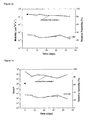
- FIG. 1 a is a graph of the mobility of compound 2 in air depending on the relative humidity
- FIG. 1 b is a graph of the on/off ratio of compound 2 in air depending on the relative humidity
- FIG. 1 c graphs a correlation between the threshold voltage and time in air.
- the compounds of the formula (I) are selected from compounds of the formula (I.A)
- R 1 , R 2 , R 3 and R 4 are each as defined above and in detail below.
- the compounds of the formula (I) are selected from compounds of the formulae (I.B)
- R a and R b are each independently 1H,1H-perfluoro-C 2 -C 30 -alkyl, 1H,1H,2H,2H-perfluoro-C 3 -C 30 -alkyl or branched C 3 -C 30 -alkyl.
- the R 1 and R 3 radicals are each chlorine and the R 2 and R 4 radicals are each hydrogen.
- the R 1 and R 4 radicals are each chlorine and the R 2 and R 3 radicals are each hydrogen.
- the R 1 , R 2 and R 3 radicals are each chlorine and the R 4 radicals are each hydrogen.
- the R 1 , R 2 , R 3 and R 4 radicals are each chlorine.
- the expression “unsubstituted or substituted alkyl, alkenyl, alkadienyl, alkynyl, cycloalkyl, bicycloalkyl, cycloalkenyl, heterocycloalkyl, aryl or heteroaryl” refers to unsubstituted or substituted alkyl, unsubstituted or substituted alkenyl, unsubstituted or substituted alkadienyl, unsubstituted or substituted alkynyl, unsubstituted or substituted cycloalkyl, unsubstituted or substituted bicycloalkyl, unsubstituted or substituted cycloalkenyl, unsubstituted or substituted heterocycloalkyl, unsubstituted or substituted aryl or unsubstituted or substituted heteroaryl.
- alkyl comprises straight-chain or branched alkyl. It is preferably straight-chain or branched C 1 -C 70 -alkyl, especially C 1 -C 30 -alkyl, more especially C 1 -C 20 -alkyl, e.g. C 1 -C 12 -alkyl.
- alkyl groups are especially methyl, ethyl, n-propyl, isopropyl, n-butyl, isobutyl, sec-butyl, tert-butyl, n-pentyl, n-hexyl, n-heptyl, n-octyl, n-nonyl, n-decyl, n-undecyl, n-dodecyl, n-tridecyl, n-tetradecyl, n-hexadecyl, n-octadecyl and n-eicosyl.
- Preferred branched alkyl groups are swallowtail alkyl groups (see below).
- alkyl also comprises alkyl radicals whose carbon chains may be interrupted by one or more nonadjacent groups which are selected from —O—, —S—, —NR e —, —C( ⁇ O)—, —S( ⁇ O)— and/or —S( ⁇ O) 2 —.
- R e is preferably hydrogen, alkyl, cycloalkyl, heterocycloalkyl, aryl or hetaryl.
- the expression alkyl also comprises substituted alkyl radicals. Substituted alkyl groups may, depending on the length of the alkyl chain, have one or more (e.g. 1, 2, 3, 4, 5 or more than 5) substituents.
- Halogen substituents are preferably fluorine, chlorine or bromine.
- Carboxylate and sulfonate are, respectively, a derivative of a carboxylic acid function or a sulfonic acid function, especially a metal carboxylate or sulfonate, a carboxylic ester or sulfonic ester function or a carboxamide or sulfonamide function.
- Cycloalkyl, heterocycloalkyl, aryl and hetaryl substituents of the alkyl groups may in turn be unsubstituted or substituted; suitable substituents are those specified below for these groups.
- alkyl also apply to the alkyl moieties in alkoxy, alkylamino, alkylthio, alkylsulfinyl, alkylsulfonyl, etc.
- arylalkyl Aryl-substituted alkyl radicals (“arylalkyl”) have at least one unsubstituted or substituted aryl group as defined below.
- the alkyl group in “arylalkyl” may bear at least one further substituent and/or be interrupted by one or more nonadjacent groups which are selected from —O—, —S—, —NR e —, —CO— and/or —SO 2 —.
- R e has one of the meanings given above.
- Arylalkyl is preferably phenyl-C 1 -C 10- alkyl, more preferably phenyl-C 1 -C 4 -alkyl, for example benzyl, 1-phenethyl, 2-phenethyl, 1-phenprop-1-yl, 2-phenprop-1-yl, 3-phenprop-1-yl, 1-phenbut-1-yl, 2-phenbut-1-yl, 3-phenbut-1-yl, 4-phenbut-1-yl, 1-phenbut-2-yl, 2-phenbut-2-yl, 3-phenbut-2-yl, 4-phenbut-2-yl, 1-(phenmeth)eth-1-yl, 1-(phenmethyl)-1-(methyl)eth-1-yl or (phenmethyl)-1-(methyl)prop-1-yl; preferably benzyl and 2-phenethyl.
- alkenyl comprises straight-chain and branched alkenyl groups which, depending on the chain length, may bear one or more noncumulated carbon-carbon double bonds (e.g. 1, 2, 3, 4 or more than 4). Alkenyl which has two double bonds is also referred to hereinafter as alkadienyl. Preference is given to C 2 -C 18 —, particular preference to C 2 -C 12 -alkenyl groups.
- alkenyl also comprises substituted alkenyl groups which may bear one or more (e.g. 1, 2, 3, 4, 5 or more than 5) substituents.
- Suitable substituents are, for example, selected from cycloalkyl, heterocycloalkyl, aryl, hetaryl, halogen, hydroxyl, alkoxy, alkylthio, mercapto, COOH, carboxylate, SO 3 H, sulfonate, NE 3 E 4 , nitro and cyano, where E 3 and E 4 are each independently hydrogen, alkyl, cycloalkyl, heterocycloalkyl, aryl or hetaryl.
- Alkenyl is then, for example, ethenyl, 1-propenyl, 2-propenyl, 1-butenyl, 2-butenyl, 3-butenyl, 1-pentenyl, 2-pentenyl, 3-pentenyl, 4-pentenyl, 1-hexenyl, 2-hexenyl, 3-hexenyl, 4-pentenyl, 1-hexenyl, 2-hexenyl, 3-hexenyl, 4-hexenyl, 5-hexenyl, penta-1,3-dien-1-yl, hexa-1,4-dien-1-yl, hexa-1,4-dien-3-yl, hexa-1,4-dien-6-yl, hexa-1,5-dien-1-yl, hexa-1,5-dien-3-yl, hexa-1,5-dien-4-yl, hepta-1,4-dien-1-yl, h
- alkynyl comprises unsubstituted or substituted alkynyl groups which have one or more nonadjacent triple bonds, such as ethynyl, 1-propynyl, 2-propynyl, 1-butynyl, 2-butynyl, 3-butynyl, 1-pentynyl, 2-pentynyl, 3-pentynyl, 4-pentynyl, 1-hexynyl, 2-hexynyl, 3-hexynyl, 4-hexynyl, 5-hexynyl, and the like.
- alkynyl also apply to the alkynyl groups in alkynyloxy, alkynylthio, etc.
- Substituted alkynyls preferably bear one or more (e.g. 1, 2, 3, 4, 5 or more than 5) of the substituents specified above for alkenyl.
- cycloalkyl comprises unsubstituted or else substituted cycloalkyl groups, preferably C 3 -C 8 -cycloalkyl groups such as cyclopropyl, cyclobutyl, cyclopentyl, cyclohexyl, cycloheptyl or cyclooctyl, especially C 5 -C 8 -cycloalkyl.
- Substituted cycloalkyl groups may have one or more (e.g. 1, 2, 3, 4, 5 or more than 5) substituents. These are preferably each independently selected from alkyl, alkoxy, alkylthio and the substituents specified above for the alkyl groups.
- the cycloalkyl groups preferably bear one or more, for example one, two, three, four or five, C 1 -C 6 -alkyl groups.
- cycloalkyl groups are cyclopentyl, 2- and 3-methylcyclopentyl, 2- and 3-ethylcyclopentyl, cyclohexyl, 2-, 3- and 4-methylcyclohexyl, 2-, 3- and 4-ethylcyclohexyl, 2-, 3- and 4-propylcyclohexyl, 2-, 3- and 4-isopropylcyclohexyl, 2-, 3- and 4-butylcyclohexyl, 2-, 3- and 4-sec-butylcyclohexyl, 2-, 3- and 4-tert-butylcyclohexyl, cycloheptyl, 2-, 3- and 4-methylcycloheptyl, 2-, 3- and 4-ethylcycloheptyl, 2-, 3- and 4-propylcycloheptyl, 2-, 3- and 4-isopropylcycloheptyl, 2-, 3- and 4-butylcycloheptyl, 2-, 3- and 4-sec-butylcyclohe
- cycloalkenyl comprises unsubstituted and substituted monounsaturated hydrocarbon groups having from 3 to 8, preferably from 5 to 6 carbon ring members, such as cyclopenten-1-yl, cyclopenten-3-yl, cyclohexen-1-yl, cyclohexen-3-yl, cyclohexen-4-yl and the like. Suitable substituents are those specified above for cycloalkyl.
- bicycloalkyl preferably comprises bicyclic hydrocarbon radicals having from 5 to 10 carbon atoms, such as bicyclo[2.2.1]hept-1-yl, bicyclo[2.2.1]hept-2-yl, bicyclo[2.2.1]hept-7-yl, bicyclo[2.2.2]oct-1-yl, bicyclo[2.2.2]oct-2-yl, bicyclo[3.3.0]octyl, bicyclo[4.4.0]decyl and the like.
- the expression “bicycloalkyl” comprises unsubstituted or else substituted bicycloalkyl groups.
- Substituted bicycloalkyl groups may have one or more (e.g. 1, 2, 3 or more than 3) substituents. These are preferably each independently selected from alkyl, alkoxy, alkylthio, and the substituents specified above for the alkyl groups.
- aryl comprises mono- or polycyclic aromatic hydrocarbon radicals which may be unsubstituted or substituted.
- Aryl is preferably unsubstituted or substituted phenyl, naphthyl, indenyl, fluorenyl, anthracenyl, phenanthrenyl, naphthacenyl, chrysenyl, pyrenyl, etc., and more preferably phenyl or naphthyl.
- Substituted aryls may, depending on the number and size of their ring systems, have one or more (e.g. 1, 2, 3, 4, 5 or more than 5) substituents.
- E 5 and E 6 are each independently hydrogen, alkyl, cycloalkyl, heterocycloalkyl, aryl or hetaryl.
- Halogen substituents are preferably fluorine, chlorine or bromine.
- Aryl is more preferably phenyl which, in the case of substitution, may bear generally 1, 2, 3, 4 or 5, preferably 1, 2 or 3 substituents.
- Aryl which bears one or more radicals is, for example, 2-, 3- and 4-methylphenyl, 2,4-, 2,5-, 3,5- and 2,6-dimethylphenyl, 2,4,6-trimethylphenyl, 2-, 3- and 4-ethylphenyl, 2,4-, 2,5-, 3,5- and 2,6-diethylphenyl, 2,4,6-triethylphenyl, 2-, 3- and 4-propylphenyl, 2,4-, 2,5-, 3,5- and 2,6-dipropylphenyl, 2,4,6-tripropylphenyl, 2-, 3- and 4-isopropylphenyl, 2,4-, 2,5-, 3,5- and 2,6-diisopropylphenyl, 2,4,6-triisopropylphenyl, 2-, 3- and 4-butylphenyl, 2,4-, 2,5-, 3,5- and 2,6-dibutylphenyl, 2,4,6-tributylphenyl, 2-, 3-
- heterocycloalkyl comprises nonaromatic, unsaturated or fully saturated, cycloaliphatic groups having generally from 5 to 8 ring atoms, preferably 5 or 6 ring atoms, in which 1, 2 or 3 of the ring carbon atoms are replaced by heteroatoms selected from oxygen, nitrogen, sulfur and an —NR e — group and which is unsubstituted or substituted by one or more, for example 1, 2, 3, 4, 5 or 6 C 1 -C 6 -alkyl groups.
- R e is as defined above.
- heterocycloaliphatic groups include pyrrolidinyl, piperidinyl, 2,2,6,6-tetramethylpiperidinyl, imidazolidinyl, pyrazolidinyl, oxazolidinyl, morpholidinyl, thiazolidinyl, isothiazolidinyl, isoxazolidinyl, piperazinyl, tetrahydrothiophenyl, dihydrothien-2-yl, tetrahydrofuranyl, dihydrofuran-2-yl, tetrahydropyranyl, 1,2-oxazolin-5-yl, 1,3-oxazolin-2-yl and dioxanyl.
- heteroaryl comprises unsubstituted or substituted, heteroaromatic, mono- or polycyclic groups, preferably the pyridyl, quinolinyl, acridinyl, pyridazinyl, pyrimidinyl, pyrazinyl, pyrrolyl, imidazolyl, pyrazolyl, indolyl, purinyl, indazolyl, benzotriazolyl, 1,2,3-triazolyl, 1,3,4-triazolyl and carbazolyl groups, where these heterocycloaromatic groups, in the case of substitution, may bear generally 1, 2 or 3 substituents.
- the substituents are preferably selected from C 1 -C 6 -alkyl, C 1 -C 6 -alkoxy, hydroxyl, carboxyl, halogen and cyano.
- Nitrogen-containing 5- to 7-membered heterocycloalkyl or heteroaryl radicals which optionally comprise further heteroatoms selected from oxygen and sulfur comprise, for example, pyrrolyl, pyrazolyl, imidazolyl, triazolyl, pyrrolidinyl, pyrazolinyl, pyrazolidinyl, imidazolinyl, imidazolidinyl, pyridinyl, pyridazinyl, pyrimidinyl, pyrazinyl, triazinyl, piperidinyl, piperazinyl, oxazolyl, isooxazolyl, thiazolyl, isothiazolyl, indolyl, quinolinyl, isoquinolinyl or quinaldinyl.
- Halogen is fluorine, chlorine, bromine or iodine.
- the R a and R b radicals may be defined identically or differently. In a preferred embodiment, the R a and R b radicals have identical definitions.
- the R a and R b radicals are both hydrogen.
- R a and R b radicals other than hydrogen are:
- sulfomethyl 2-sulfoethyl, 3-sulfopropyl, 4-sulfobutyl, 5-sulfopentyl, 6-sulfohexyl, 8-sulfooctyl, 10-sulfodecyl, 12-sulfododecyl and 14-sulfotetradecyl;
- ethynyl 1- and 2-propynyl, 1-, 2- and 3-butynyl, 1-, 2-, 3- and 4-pentynyl, 1-, 2-, 3-, 4- and 5-hexynyl, 1-, 2-, 3-, 4-, 5-, 6-, 7-, 8- and 9-decynyl, 1-, 2-, 3-, 4-, 5, 6-, 7, 8-, 9, 10- and 11-dodecynyl and 1-, 2-, 3-, 4-, 5-, 6-, 7-, 8-, 9-, 10-, 11, 12-, 13-, 14-, 15-, 16- and 17-octadecynyl;
- ethenyl 1- and 2-propenyl, 1-, 2- and 3-butenyl, 1-, 2-, 3- and 4-pentenyl, 1-, 2-, 3-, 4- and 5-hexenyl, 1-, 2-, 3-, 4-, 5-, 6-, 7-, 8- and 9-decenyl, 1-, 2-, 3-, 4-, 5-, 6-, 7-, 8-, 9-, 10- and 11-dodecenyl and 1-, 2-, 3-, 4-, 5-, 6-, 7-, 8-, 9-, 10-, 11-, 12-, 13-, 14-, 15-, 16- and 17-octadecenyl;
- carbamoyl methylaminocarbonyl, ethylaminocarbonyl, propylaminocarbonyl, butylaminocarbonyl, pentylaminocarbonyl, hexylaminocarbonyl, heptylaminocarbonyl, octylaminocarbonyl, nonylaminocarbonyl, decylaminocarbonyl and phenylaminocarbonyl;
- aminosulfonyl N-dodecylaminosulfonyl, N,N-diphenylaminosulfonyl, and, N-bis(4-chlorophenyl)aminosulfonyl;
- methoxysulfonyl methoxysulfonyl, ethoxysulfonyl, propoxysulfonyl, butoxysulfonyl, hexoxysulfonyl, dodecyloxysulfonyl, octadecyloxysulfonyl, phenoxysulfonyl, 1- and 2-naphthyloxysulfonyl, (4-tert-butylphenoxy)sulfonyl and (4-chlorophenoxy)sulfonyl;
- 2-dioxanyl 1-morpholinyl, 1-thiomorpholinyl, 2- and 3-tetrahydrofuryl, 1-, 2- and 3-pyrrolidinyl, 1-piperazyl, 1-diketopiperazyl and 1-, 2-, 3- and 4-piperidyl;
- R a and R b radicals are as follows:
- the R a and R b radicals are each independently 1H,1H-perfluoro-C 2 -C 30 -alkyl or 1H,1H,2H,2H-perfluoro-C 3 -C 30 -alkyl, preferably 1H,1H-perfluoro-C 2 -C 20 -alkyl or 1H,1H,2H,2H-perfluoro-C 3 -C 20 -alkyl, in particular 1H,1H-perfluoro-C 2 -C 10 -alkyl or 1H,1H,2H,2H-perfluoro-C 3 -C 10 -alkyl such as 2,2,2-trifluoroethyl, 2,2,3,3,3-pentafluoropropyl, 2,2,3,3,4,4,4-heptafluorobutyl, 1H,1H-perfluoropentyl, 1H,1H-perfluorohexyl
- R a and R b radicals are selected from groups of the general formula (II) #-(A) p -C(R f ) x (II)
- a preferred radical of the formula (II) is, for example, 2-ethylhex-1-yl.
- the R a and R b radicals are more preferably selected from groups of the formula (II.1) (so-called swallowtail radicals).
- the R f radicals are selected from C 1 -C 30 -alkyl, preferably C 1 -C 12 -alkyl, more preferably C 1 -C 8 -alkyl, e.g. C 4 -C 8 -alkyl, preferably C 5 -C 7 -alkyl.
- the R a and R b radicals are then preferably both a group of the formula
- Preferred radicals of the formula II.1 are for example:
- More preferred radicals are for example:
- Very preferred examples of a group of the formula II.1), wherein each R f has the same meaning are 1-butylpent-1-yl, 1-pentylhex-1-yl and 1-hexylhept-1-yl.
- Preferred examples of a group of the formula II.1), wherein each R f has a different meaning are 2-ethylhexyl, 1-methylbutyl, 1-methylpentyl or 1-methylhexyl.
- R a is selected from groups of the formula (III.A): —(C n H 2n )—R a1 and R b is selected from groups of the formula (III.B): —(C n H 2n )—R b1 , where R a1 and R b1 are each independently selected from unsubstituted or substituted cycloalkyl, bicycloalkyl, cycloalkenyl, heterocycloalkyl, aryl and hetaryl, and n is an integer from 1 to 4.
- R a is then preferably selected from —CH 2 —R a1 , —CH 2 CH 2 —R a1 , —CH 2 CH 2 CH 2 —R a1 and —CH 2 CH 2 CH 2 CH 2 —R a1 .
- R b is then preferably selected from —CH 2 —R b1 , —CH 2 CH 2 —R b1 , —CH 2 CH 2 CH 2 —R b1 and —CH 2 CH 2 CH 2 CH 2 —R b1 .
- R a1 and R b1 are then preferably selected from groups of the general formulae (1) to (16)
- n in the formulae (C n H 2n )—R a1 and (C n H 2n )—R b1 is 1 or 2.
- R a and R b are both
- # represents the bonding site to an imide nitrogen atom.
- R a and R b are selected from 1,1-dihydroperfluoro-C 2 -C 9 -alkyl groups, in particular 1,1-dihydroperfluoro-C 2 -C 6 -alkyl groups.
- R a and R b are then selected from groups of the general formula (IV) #—CH 2 -(perfluoro-C 1 -C 9 -alkyl) (IV)
- # represents the bonding site to an imide nitrogen atom, in particular from #—CH 2 -(perfluoro-C 1 -C 5 -alkyl).
- Preferred perfluoro-C 1 -C 5 -alkyl radicals in the formula (IV) are trifluoromethyl, pentafluoroethyl, n-heptafluoropropyl (n-C 3 F 7 ), heptafluoroisopropyl (CF(CF 3 ) 2 ), n-nonafluorobutyl (n-C 4 F 9 ), n-undecafluoropentyl (n-C 5 F 11 ), and also C(CF 3 ) 3 , CF 2 CF(CF 3 ) 2 , CF(CF 3 )(C 2 F 5 ).
- Preferred perfluoro-C 6 -C 9 -alkyl radicals in the formula (IV) include n-C 6 F 13 , n-C 7 F 15 , n-C 8 F 17 or n-C 9 F 19 .
- R a and R b are the same.
- R a and R b are both —CH 2 -(n-C 3 F 7 ) or CH 2 -(n-C 4 F 9 ).
- R a and R b are selected from 1,1,2,2-tetrahydroperfluoro-C 3 -C 10 -alkyl groups.
- R a and R b are then selected from groups of the general formula (V) #—CH 2 —CH 2 -(perfluoro-C 1 -C 8 -alkyl) (V)
- # represents the bonding site to an imide nitrogen atom.
- Preferred perfluoro-C 1 -C 8 -alkyl radicals in the formula (V) are trifluoromethyl, pentafluoroethyl, n-heptafluoropropyl (n-C 3 F 7 ), heptafluoroisopropyl (CF(CF 3 ) 2 ), n-nonafluorobutyl (n-C 4 F 9 ), n-undecafluoropentyl (n-C 5 F 11 ), n-C 6 F 13 , n-C 7 F 15 , n-C 8 F 17 , C(CF 3 ) 3 , CF 2 CF(CF 3 ) 2 , or CF(CF 3 )(C 2 F 5 ).
- R a and R b are the same.
- R a and R b are each selected from fluorophenylalkyl groups of the general formula (VI)
- m is preferably 5.
- n is preferably 2.
- the fluorophenylalkyl groups of the general formula (VI) are preferably selected from
- the fluorophenylalkyl groups are more preferably selected from groups of the formulae
- A is especially (CH 2 ) 2 .
- R a and R b are both
- # represents the bonding site to an imide nitrogen atom.
- R a and R b are selected from fluorophenyl groups of the general formula (VII)
- R a and R b are both
- # represents the bonding site to an imide nitrogen atom.
- a further object of the present invention relates to novel tri- and tetrachlorinated naphthalene compounds of the formula (I), except of 2,3,6,7-tetrachloronaphthalene-1,4,5,8-tetracarboxylic dianhydride and 2,3,6,7-tetrachloronaphthalene-1,4,5,8-tetracarboxylic dimid.
- Z 1 , Z 2 , Z 3 , Z 4 are each O;
- Y 1 is NR a with R a being 1H,1H-perfluoro-C 2 -C 30 -alkyl or 1H,1H,2H,2H-perfluoro-C 3 -C 30 -alkyl;
- Y 2 is NR b with R b being 1H,1H-perfluoro-C 2 -C 30 -alkyl or 1H,1H,2H,2H-perfluoro-C 3 -C 30 -alkyl;
- R 1 , R 2 and R 3 are each Cl and
- R 4 is hydrogen, or R 1 , R 2 , R 3 and R 4 are each Cl.
- a further object of the present invention are dichlorinated naphthalenetetracarboxylic diimide compounds of the formula (I.Ba)
- the invention further provides a process for preparing compounds of the formula (I.A)
- Naphthalene-1,8:4,5-tetracarboxylic dianhydride can be chlorinated by reaction with chlorine in chlorosulfonic acid as a solvent.
- the reaction of the naphthalene-1,8:4,5-tetracarboxylic dianhydride with a chlorinating agent preferably takes place in the presence of iodine as a catalyst.
- the temperature and the duration of the chlorination can be used to control the degree of chlorination of the compounds (I.A).
- the reaction temperature for the reaction with a chlorinating agent is typically within a range from 35 to 150° C., preferably 35 to 110° C., more preferably from 60 to 100° C., e.g. from 40 to 95° C.
- the reaction of the naphthalene-1,8:4,5-tetracarboxylic dianhydride with a chlorinating agent can be brought about under standard pressure or under elevated pressure, e.g. the chlorination pressure is in the range from 1 bar to 100 bar. Usually the chlorination pressure is in the range from 1 to 10 bar.
- the compounds of the formula (I.A) are isolated from the reaction mixture typically by precipitation.
- the precipitation is brought about, for example, by adding a liquid which does not dissolve the compounds or does so only to a minor degree, but is miscible with the inert solvents.
- a preferred precipitant is water.
- the precipitation products can then be isolated by filtration and typically have a sufficiently high purity.
- 2,3,6,7-Tetrachloronaphthalene-1,4,5,8-tetracarboxylic dianhydride can also be prepared according to the method described in DE 36 20 332.
- the compounds of the formula (I.A) may be advantageous to subject the compounds of the formula (I.A) to a further purification.
- a further purification examples include column chromatography methods, in which case the products, dissolved, for example, in a halogenated hydrocarbon such as methylene chloride or a toluene/- or petroleum ether/ethyl acetate mixture, are subjected to a separation or filtration on silica gel.
- a halogenated hydrocarbon such as methylene chloride or a toluene/- or petroleum ether/ethyl acetate mixture
- purification by sublimation or crystallization is possible.
- the purification steps are repeated once or more than once and/or different purification steps are combined in order to obtain very pure compounds (I.A).
- the invention further provides a process for preparing compounds of the formulae (I.B)
- reaction step a1) With regard to reaction step a1), reference is made to the above remarks regarding the chlorination of naphthalene-1,8:4,5-tetracarboxylic dianhydride.
- the imidation of the carboxylic anhydride groups in reaction steps b1) is known in principle. Preference is given to reacting the anhydride with the primary amine in the presence of a polar aprotic solvent.
- Suitable polar aprotic solvents are nitrogen heterocycles such as pyridine, pyrimidine, quinoline, isoquinoline, quinaldine, N-methylpiperidine, N-methylpiperidone and N-methylpyrrolidone.
- Suitable imidation catalysts are organic and inorganic acids, for example formic acid, acetic acid, propionic acid and phosphoric acid. Suitable imidation catalysts are additionally organic and inorganic salts of transition metals, such as zinc, iron, copper and magnesium. Examples include zinc acetate, zinc propionate, zinc oxide, iron(II) acetate, iron(III) chloride, iron(II) sulfate, copper(II) acetate, copper(II) oxide and magnesium acetate.
- An imidation catalyst is used preferably in the reaction of aromatic amines and is generally also advantageous for the reaction of cycloaliphatic amines.
- the amount of the imidation catalyst used is generally from 5 to 80% by weight, more preferably from 10 to 75% by weight, based on the total weight of the compound to be amidated.
- the quantitative molar ratio of amine to dianhydride is preferably from about 2:1 to 4:1, more preferably from 2.2:1 to 3:1.
- the reaction temperature in step b1) is generally from ambient temperature to 200° C., preferably from 40° C. to 180° C.
- Aliphatic and cycloaliphatic amines are reacted preferably within a temperature range from about 60° C. to 100° C.
- Aromatic amines are reacted preferably within a temperature range from about 120° C. to 160° C.
- the reaction in step b1) is preferably effected under a protective gas atmosphere, for example nitrogen.
- the reaction in step b1) can be effected at standard pressure or if desired under elevated pressure.
- a suitable pressure range is in the range from about 0.8 to 10 bar.
- volatile amines for instance, ⁇ 180° C.
- preference is given to working under elevated pressure.
- the diimides obtained in step b1) can be used for the subsequent reactions without further purification.
- the products it may, however, be advantageous to subject the products to further purification.
- Examples include column chromatography methods, in which case the products are preferably dissolved in a halogenated hydrocarbon such as methylene chloride, chloroform or tetrachloroethane and subjected to a separation or filtration on silica gel. Finally, the solvent is removed.
- the invention further provides a process for preparing compounds of the formulae (I.B)
- the naphthalene-1,8:4,5-tetracarboxylic dianhydride is converted in step a2) by using amines of the formula R a —NH 2 and if appropriate one of the formula R b —NH 2 , in which R a and R b are each groups which cannot be chlorinated by reaction with chlorine in the presence of iodine as a catalyst.
- the chlorination of the compound of the formula (D) in step b2) is brought about by reaction with chlorine in chlorosulfonic acid and in the presence of catalytic amounts of iodine.
- the amount of iodine is 1 to 10% by weight, preferably 2 to 5% by weight, based on the amount of chlorine.
- the reaction temperature for the reaction with chlorine is typically within a range from 40 to 150° C., preferably from 60 to 100° C.
- the reaction of the naphthalene-1,8:4,5-tetracarboxylic dianhydride with chlorine can be brought about under standard pressure or under elevated pressure, e.g. the chlorination pressure is in the range from 1 bar to 100 bar. Usually the chlorination pressure is in the range from 1 bar to 10 bar.
- the reaction times usually range from 2 to 48 hours, preferably 4 to 16 hours.
- the reaction temperature and the reaction time of the chlorination can be used to control the degree of chlorination.
- R a and R b are as defined above.
- the dichloronaphthalenetetracarboxylic bisanhydrides of formulae (IX) and (X), respectively, are treated with an amine of the formula R a —NH 2 and if appropriate one of the formula R b —NH 2 , in the case that R a is different from R b .
- the reaction is usually carried out in a solvent. Suitable solvents include C 1 -C 6 alkane carboxylic acids, e.g. acetic acid.
- 2,6-Dichloronaphthalene-1,4,5,8-tetracarboxylic acid dianhydride of the formula (IX) and 2,7-dichloronaphthalene-1,4,5,8-tetracarboxylic acid dianhydride of the formula (X) i.e. compounds of the formula (I.A), wherein R 1 and R 4 are both chlorine and R 2 and R 3 are both hydrogen or R 1 and R 3 are both chlorine and R 2 and R 4 are both hydrogen, respectively
- R 1 and R 4 are both chlorine and R 2 and R 3 are both hydrogen or R 1 and R 3 are both chlorine and R 2 and R 4 are both hydrogen, respectively
- the compounds of the formula (I) and more specifically of the formulae (I.A) and (I.B) are particularly advantageously suitable as organic semiconductors. They generally function as n-type semiconductors.
- the compounds of the formula (I) used in accordance with the invention are combined with other semiconductors and the position of the energy levels has the result that the other semiconductors function as n-type semiconductors, the compounds (I) can also function as p-semiconductors in exceptional cases.
- the compounds of the formula (I) are notable for their air stability.
- organic field-effect transistors comprising a compound of formula (I) are notable for their air stability and humidity stability.
- the compounds of the formula (I) possess a high charge transport mobility and/or have a high on/off ratio.
- the compounds of the formula (I) have charge mobilities of least 0.1 cm 2 V ⁇ 1 s ⁇ 1 when deposited by vacuum-deposition methods or of least 0.01 cm 2 V ⁇ 1 s ⁇ 1 when deposited in liquid form.
- the average on/off ratio is at least 10 4 , preferably at least 10 5 . They are suitable in a particularly advantageous manner for organic field-effect transistors (OFETs).
- inventive compounds are suitable particularly advantageously for the production of integrated circuits (ICs), for which the n-channel MOSFETs (metal oxide semiconductor field-effect transistors (MOSFETs)) customary to date are used.
- ICs integrated circuits
- MOSFETs metal oxide semiconductor field-effect transistors
- CMOS-like semiconductor units for example for microprocessors, microcontrollers, static RAM, and other digital logic units.
- inventive compounds of the formula (I) can be processed further by one of the following processes: printing (offset, flexographic, gravure, screen, inkjet, electrophotography), evaporation, laser transfer, spin-coating, photolithography, dropcasting. They are suitable especially for use in displays (especially large-area and/or flexible displays) and RFID tags.
- inventive compounds are also suitable particularly as fluorescence emitters in OLEDs, in which they are excited either by electroluminescence or by an appropriate phosphorescence emitter via Förster energy transfer (FRET).
- FRET Förster energy transfer
- inventive compounds of the formula (I) are also particularly suitable in displays which switch colors on and off based on an electrophoretic effect via charged pigment dyes.
- Such electrophoretic displays are described, for example, in US 2004/0130776.
- the invention further provides organic field-effect transistors comprising a substrate having at least one gate structure, a source electrode and a drain electrode and at least one compound of the formula I as defined above as an n-type semiconductor.
- the invention further provides substrates comprising a multitude of organic field-effect transistors, wherein at least some of the field-effect transistors comprise at least one compound of the formula I as defined above as an n-type semiconductor.
- the invention also provides semiconductor units which comprise at least one such substrate.
- a specific embodiment is a substrate with a pattern (topography) of organic field-effect transistors, each transistor comprising
- the organic semiconductor consisting of at least one compound of the formula (I) or comprising a compound of the formula (I).
- the organic field-effect transistor generally comprises a dielectric.
- a further specific embodiment is a substrate having a pattern of organic field-effect transistors, each transistor forming an integrated circuit or being part of an integrated circuit and at least some of the transistors comprising at least one compound of the formula (I).
- Suitable substrates are in principle the materials known for this purpose.
- Suitable substrates comprise, for example, metals (preferably metals of groups 8, 9, 10 or 11 of the Periodic Table, such as Au, Ag, Cu), oxidic materials (such as glass, quartz, ceramics, SiO 2 ), semiconductors (e.g. doped Si, doped Ge), metal alloys (for example based on Au, Ag, Cu, etc.), semiconductor alloys, polymers (e.g.
- the substrates may be flexible or inflexible, and have a curved or planar geometry, depending on the desired use.
- a typical substrate for semiconductor units comprises a matrix (for example a quartz or polymer matrix) and, optionally, a dielectric top layer.
- Suitable dielectrics are SiO 2 , polystyrene, poly- ⁇ -methylstyrene, polyolefins (such as polypropylene, polyethylene, polyisobutene), polyvinylcarbazole, fluorinated polymers (e.g. Cytop, CYMM), cyanopullulans, polyvinylphenol, poly-p-xylene, polyvinyl chloride, or polymers crosslinkable thermally or by atmospheric moisture.
- Specific dielectrics are “self-assembled nanodielectrics”, i.e.
- polymers which are obtained from monomers comprising SiCl functionalities, for example Cl 3 SiOSiCl 3 , Cl 3 Si—(CH 2 ) 6 —SiCl 3 , Cl 3 Si—(CH 2 ) 12 —SiCl 3 , and/or which are crosslinked by atmospheric moisture or by addition of water diluted with solvents (see, for example, Faccietti Adv. Mat. 2005, 17, 1705-1725).
- hydroxyl-containing polymers such as polyvinylphenol or polyvinyl alcohol or copolymers of vinylphenol and styrene to serve as crosslinking components.
- at least one further polymer to be present during the crosslinking operation, for example polystyrene, which is then also crosslinked (see Facietti, US patent application 2006/0202195).
- the substrate may additionally have electrodes, such as gate, drain and source electrodes of OFETs, which are normally localized on the substrate (for example deposited onto or embedded into a nonconductive layer on the dielectric).
- the substrate may additionally comprise conductive gate electrodes of the OFETs, which are typically arranged below the dielectric top layer (i.e. the gate dielectric).
- an insulator layer (gate insulating layer) is present on at least part of the substrate surface.
- the insulator layer comprises at least one insulator which is preferably selected from inorganic insulators such as SiO 2 , SiN, etc., ferroelectric insulators such as Al 2 O 3 , Ta 2 O 5 , La 2 O 5 , TiO 2 , Y 2 O 3 , etc., organic insulators such as polyimides, benzocyclobutene (BCB), polyvinyl alcohols, polyacrylates, etc., and combinations thereof.
- inorganic insulators such as SiO 2 , SiN, etc.
- ferroelectric insulators such as Al 2 O 3 , Ta 2 O 5 , La 2 O 5 , TiO 2 , Y 2 O 3 , etc.
- organic insulators such as polyimides, benzocyclobutene (BCB), polyvinyl alcohols, polyacrylates, etc., and combinations thereof.
- Preferred electrically conductive materials have a specific resistance of less than 10 ⁇ 3 ohm x meter, preferably less than 10 ⁇ 4 ohm x meter, especially less than 10 ⁇ 6 or 10 ⁇ 7 ohm x meter.
- drain and source electrodes are present at least partly on the organic semiconductor material.
- the substrate may comprise further components as used customarily in semiconductor materials or ICs, such as insulators, resistors, capacitors, conductor tracks, etc.
- the electrodes may be applied by customary processes, such as evaporation, lithographic processes or another structuring process.
- the semiconductor materials may also be processed with suitable auxiliaries (polymers, surfactants) in disperse phase by printing.
- auxiliaries polymers, surfactants
- the deposition of at least one compound of the general formula I is carried out by a gas phase deposition process (physical vapor deposition, PVD).
- PVD processes are performed under high-vacuum conditions and comprise the following steps: evaporation, transport, deposition. It has been found that, surprisingly, the compounds of the general formula I are suitable particularly advantageously for use in a PVD process, since they essentially do not decompose and/or form undesired by-products.
- the material deposited is obtained in high purity. In a specific embodiment, the deposited material is obtained in the form of crystals or comprises a high crystalline content.
- At least one compound of the general formula (I) is heated to a temperature above its evaporation temperature and deposited on a substrate by cooling below the crystallization temperature.
- the temperature of the substrate in the deposition is preferably within a range from about 20 to 250° C., more preferably from 50 to 200° C.
- the resulting semiconductor layers generally have a thickness which is sufficient for ohmic contact between source and drain electrodes.
- the deposition can be effected under an inert atmosphere, for example under nitrogen, argon or helium.
- the deposition is effected typically at ambient pressure or under reduced pressure.
- a suitable pressure range is from about 10 ⁇ 7 to 1.5 bar.
- the compound of the formula (I) is preferably deposited on the substrate in a thickness of from 10 to 1000 nm, more preferably from 15 to 250 nm.
- the compound of the formula I is deposited at least partly in crystalline form.
- the above-described PVD process is suitable.
- it is possible to use previously prepared organic semiconductor crystals. Suitable processes for obtaining such crystals are described by R. A. Laudise et al.
- the compounds of the general formula (I) can also advantageously be processed from solution.
- at least one compound of the general formula (I) is applied to a substrate (and if appropriate further semiconductor materials), for example, by spin-coating.
- at least one compound of the formula (I) is applied to a substrate by solution shearing. This type of deposition is described e.g. in Adv. Mater. 2008, 20, 2588-2594. This includes the typical knife-coating methods such as airknife-coating, knife-coating, airblade-coating, squeeze-coating, roll-coating and kiss-coating.
- a solution of the compound of the formula (I) is applied to a first substrate and then a second substrate is brought into contact with the solution. Then shear energy is introduced.
- the substrate temperatures range between room temperature and a temperature being 60 to 80% of the boiling point of the used solvent to control the solvent evaporation rate. Pulling the top wafer against the stationary wafer exerts a shearing force between wafers on the solution.
- the shearing speed is usually in the range from 0.01 to 0.5 mm/sec, preferably from 0.0866 to 0.1732 mm/sec.
- Suitable compounds for hydrophobizing substrate surfaces comprise alkyltrialkoxysilanes, such as n-octadecyltrimethoxysilane, n-octadecyltriethoxysilane, n-octadecyltri(n-propyl)-oxysilane or n-octadecyltri(isopropyl)oxysilane or phenyltrichlorosilane.
- alkyltrialkoxysilanes such as n-octadecyltrimethoxysilane, n-octadecyltriethoxysilane, n-octadecyltri(n-propyl)-oxysilane or n-octadecyltri(isopropyl)oxysilane or phenyltrichlorosilane.
- the used solvent may have a low boiling point or a high boiling point.
- Suitable solvents are aromatic solvents such as toluene, xylene, mesitylene, naphthalene, decahydronaphthalene, octahydronaphthalene, chlorobenzene or dichlorobenzene, especially ortho-dichlorobenzene, or linear or cyclic ethers, e.g.
- tetrahydrofuran diglycol methyl ether, or aromatic ethers such as diphenylether methoxybenzene, perfluoropolyethers such as HT-60 or HT 90 CT 135 (from Solvay, copolymers of perfluoroethyleneglycol, perfluoropropyleneglycol with CF 3 radicals at the beginning and the end of the chain), C 1 -C 6 -alkylesters of C 1 -C 6 -carboxylic acids such as methyl acetate, ethyl acetate, propyl acetate, butyl acetate, methyl propionate, ethyl propionate, propyl propionate, butyl propionate and mixtures thereof.
- a mixture of solvents is used, especially one, wherein the at least two solvents have different boiling points.
- the difference in the boiling points is greater than 30° C.
- the compounds of the formula (I) are also suitable for producing semiconductor elements, especially OFETs, by a printing process. It is possible for this purpose to use customary printing processes (inkjet, flexographic, offset, gravure; intaglio printing, nanoprinting).
- Preferred solvents for the use of the compounds of the formula (I) in a printing process are aromatic solvents such as toluene, xylene, cyclic ethers such as dioxane, tetrahydrofuran, or linear ethers such as dimethoxyethane, ethylene glycol diethlyether, tert-butylmethylether etc. It is also possible to add thickening substances such as polymers, for example polystyrene, etc., to these “semiconductor inks”. In this case, the dielectrics used are the aforementioned compounds.
- the inventive field-effect transistor is a thin-film transistor (TFT).
- TFT thin-film transistor
- a thin-film transistor has a gate electrode disposed on the substrate, a gate insulator layer disposed thereon and on the substrate, a semiconductor layer disposed on the gate insulator layer, an ohmic contact layer on the semiconductor layer, and a source electrode and a drain electrode on the ohmic contact layer.
- the surface of the substrate before the deposition of at least one compound of the general formula (I) (and if appropriate of at least one further semiconductor material), is subjected to a modification.
- This modification serves to form regions which bind the semiconductor materials and/or regions on which no semiconductor materials can be deposited.
- the surface of the substrate is preferably modified with at least one compound (C1) which is suitable for binding to the surface of the substrate and to the compounds of the formula (I).
- a portion of the surface or the complete surface of the substrate is coated with at least one compound (C1) in order to enable improved deposition of at least one compound of the general formula (I) (and if appropriate further semiconductive compounds).
- a further embodiment comprises the deposition of a pattern of compounds of the general formula (C1) on the substrate by a corresponding production process.
- These include the mask processes known for this purpose and so-called “patterning” processes, as described, for example, in US-2007-0190783-A1, which is incorporated here fully by reference.
- Suitable compounds of the formula (C1) are capable of a binding interaction both with the substrate and with at least one semiconductor compound of the general formula I.
- binding interaction comprises the formation of a chemical bond (covalent bond), ionic bond, coordinative interaction, van der Waals interactions, e.g. dipole-dipole interactions etc., and combinations thereof.
- Suitable compounds of the general formula (C1) are:
- the compound (C1) is preferably selected from alkyltrialkoxysilanes, especially n-octadecyltrimethoxysilane, n-octadecyltriethoxysilane; phenyltrichlorosiliane; hexaalkyldisilazanes, and especially hexamethyidisilazane (HMDS); C 8 -C 30 -alkylthiols, especially hexadecanethiol; mercaptocarboxylic acids and mercaptosulfonic acids, especially mercaptoacetic acid, 3-mercaptopropionic acid, mercaptosuccinic acid, 3-mercapto-1-propanesulfonic acid and the alkali metal and ammonium salts thereof.
- alkyltrialkoxysilanes especially n-octadecyltrimethoxysilane, n-octadecyltri
- top contact for example top contact, top gate, bottom contact, bottom gate, or else a vertical construction, for example a VOFET (vertical organic field-effect transistor), as described, for example, in US 2004/0046182.
- VOFET vertical organic field-effect transistor
- the layer thicknesses are, for example, from 10 nm to 5 ⁇ m in semiconductors, from 50 nm to 10 ⁇ m in the dielectric; the electrodes may, for example, be from 20 nm to 1 ⁇ m thick.
- the OFETs may also be combined to form other components such as ring oscillators or inverters.
- a further aspect of the invention is the provision of electronic components which comprise a plurality of semiconductor components, which may be n- and/or p-semiconductors.
- semiconductor components which may be n- and/or p-semiconductors.
- FETs field-effect transistors
- BJTs bipolar junction transistors
- tunnel diodes converters
- light-emitting components biological and chemical detectors or sensors
- temperature-dependent detectors temperature-dependent detectors
- photodetectors such as polarization-sensitive photodetectors, gates, AND, NAND, NOT, OR, TOR and NOR gates, registers, switches, timer units, static or dynamic stores and other dynamic or sequential, logical or other digital components including programmable circuits.
- a specific semiconductor element is an inverter.
- the inverter In digital logic, the inverter is a gate which inverts an input signal.
- the inverter is also referred to as a NOT gate.
- Real inverter circuits have an output current which constitutes the opposite of the input current. Typical values are, for example, (0, +5V) for TTL circuits.
- the performance of a digital inverter reproduces the voltage transfer curve (VTC), i.e. the plot of input current against output current. Ideally, it is a staged function, and the closer the real measured curve approximates to such a stage, the better the inverter is.
- VTC voltage transfer curve
- the compounds of the formula (I) are used as organic n-type semiconductors in an inverter.
- inventive compounds of the formula (I) and more specifically of the formulae (I.A) and (I.B), are also suitable particularly advantageously for use in organic photovoltaics (OPV).
- Organic solar cells generally have a layer structure and generally comprise at least the following layers: anode, photoactive layer and cathode. These layers are generally situated on a substrate customary therefore.
- the structure of organic solar cells is described, for example, in US 2005/0098726 and US 2005/0224905, which are fully incorporated here by reference.
- the invention further provides an organic solar cell comprising at least one compound of the formula I as defined above as a photoactive material.
- Suitable substrates for organic solar cells are, for example, oxidic materials (such as glass, ceramic, SiO 2 , in particular quartz, etc.), polymers (e.g. polyvinyl chloride, polyolefins such as polyethylene and polypropylene, polyesters, fluoropolymers, polyamides, polyurethanes, polyalkyl(meth)acrylates, polystyrene and mixtures and composites thereof) and combinations thereof.
- oxidic materials such as glass, ceramic, SiO 2 , in particular quartz, etc.
- polymers e.g. polyvinyl chloride, polyolefins such as polyethylene and polypropylene, polyesters, fluoropolymers, polyamides, polyurethanes, polyalkyl(meth)acrylates, polystyrene and mixtures and composites thereof.
- Suitable electrodes are in principle metals (preferably of groups 8, 9, 10 or 11 of the Periodic Table, e.g. Pt, Au, Ag, Cu, Al, In, Mg, Ca), semiconductors (e.g. doped Si, doped Ge, indium tin oxide (ITO), gallium indium tin oxide (GITO), zinc indium tin oxide (ZITO), etc.), metal alloys (e.g. based on Pt, Au, Ag, Cu, etc., especially Mg/Ag alloys), semiconductor alloys, etc.
- One of the electrodes, e.g. theanode used is preferably a material essentially transparent to incident light.
- the other electrode e.g. the cathode used is preferably a material which essentially reflects the incident light.
- the photoactive layer itself comprises at least one, or consists of at least one, layer which has been provided by a process according to the invention and comprises, as an organic semiconductor material, at least one compound of the formula Ia and/or Ib as defined above.
- further layers include, for example,
- Suitable exciton- and hole-blocking layers are described, for example, in U.S. Pat. No. 6,451,415.
- Suitable materials for exciton blocker layers are, for example, bathocuproin (BCP), 4,4′,4′′-tris[3-methylphenyl-N-phenylamino]triphenylamine (m-MTDATA) or polyethylenedioxythiophene (PEDOT).
- BCP bathocuproin
- m-MTDATA 4,4′,4′′-tris[3-methylphenyl-N-phenylamino]triphenylamine
- PEDOT polyethylenedioxythiophene
- the inventive solar cells may be based on photoactive donor-acceptor heterojunctions.
- HTM hole transport material
- ETM electron transport material
- Suitable ETMs are, for example, C60 and other fullerenes, perylene-3,4:9,10-bis(dicarboximides) (PTCDI), etc.
- PTCDI perylene-3,4:9,10-bis(dicarboximides)
- the complementary HTM has to be selected such that, after excitation of the compound, a rapid hole transition to the HTM takes place.
- the heterojunction may have a flat (smooth) design (cf.
- the heterojunction may also be designed as a bulk heterojunction or interpenetrating donor-acceptor network (cf., for example, C. J. Brabec, N. S. Sariciftci, J. C. Hummelen, Adv. Funct. Mater., 11 (1), 15 (2001)).
- the compounds of the formula I may be used as a photoactive material in solar cells with MiM, pin, pn, Mip or Min structure
- the compounds of the formula I can also be used as photoactive material in tandem cells, as described by P. Peumans, A. Yakimov, S. R. Forrest in J. Appl. Phys, 93 (7), 3693-3723 (2003) (cf. U.S. Pat. No. 4,461,922, U.S. Pat. No. 6,198,091 and U.S. Pat. No. 6,198,092).
- the compounds of the formula I may also be used as photoactive material in tandem cells composed of two or more stacked MiM, pin, Mip or Min diodes (cf. patent application DE 103 13 232.5) (J. Drechsel et al., Thin Solid Films, 451452, 515-517 (2004)).
- the layer thicknesses of the M, n, i and p layers are typically from 10 to 1000 nm, preferably from 10 to 400 nm, more preferably from 10 to 100 nm.
- Thin layers can be produced by vapor deposition under reduced pressure or in inert gas atmosphere, by laser ablation or by solution- or dispersion-processible processes such as spin-coating, knife-coating, casting processes, spraying, dip-coating or printing (e.g. inkjet, flexographic, offset, gravure; intaglio printing, nanoimprinting).
- Suitable organic solar cells may, as mentioned above, comprise at least one inventive compound of the formula I as an electron donor (n-type semiconductor) or electron acceptor (p-semiconductor).
- inventive compound of the formula I as an electron donor (n-type semiconductor) or electron acceptor (p-semiconductor).
- the following semiconductor materials are suitable for use in organic photovoltaics:
- Phthalocyanines which are unhalogenated or halogenated. These include metal-free phthalocyanines or phthalocyanines comprising divalent metals or groups containing metal atoms, especially those of titanyloxy, vanadyloxy, iron, copper, zinc, etc. Suitable phthalocyanines are especially copper phthalocyanine, zinc phthalocyanine and metal-free phthalocyanine. In a specific embodiment, a halogenated phthalocyanine is used. These include:
- 2,6,10,14-tetrafluorophthalocyanines e.g. copper 2,6,10,14-tetrafluorophthalocyanine and zinc 2,6,10,14-tetrafluorophthalocyanine;
- 1,5,9,13-tetrafluorophthalocyanines e.g. copper 1,5,9,13-tetrafluorophthalocyanine and zinc 1,5,9,13-tetrafluorophthalocyanine;
- 2,3,6,7,10,11,14,15-octafluorophthalocyanine e.g. copper 2,3,6,7,10,11,14,15-octafluorophthalocyanine and zinc 2,3,6,7,10,11,14,15-octafluorophthalocyanine; hexadecachlorophthalocyanines and hexadecafluorophthalocyanines, such as copper hexadecachlorophthalocyanine, zinc hexadecachlorophthalocyanine, metal-free hexadecachlorophthalocyanine, copper hexadecafluorophthalocyanine, hexadecafluorophthalocyanine or metal-free hexadefluorophthalocyanine.
- hexadecachlorophthalocyanines and hexadecafluorophthalocyanines such as copper hexadecachlorophthalocyanine, zinc hexa
- Porphyrins for example 5,10,15,20-tetra(3-pyridyl)porphyrin (TpyP), or else tetrabenzoporphyrins, for example metal-free tetrabenzoporphyrin, copper tetrabenzoporphyrin or zinc tetrabenzoporphyrin.
- tetrabenzoporphyrins which, like the compounds of the formula (I) used in accordance with the invention, are processed from solution as soluble precursors and are converted to the pigmentary photoactive component by thermolysis on the substrate.
- Acenes such as anthracene, tetracene, pentacene, each of which may be unsubstituted or substituted.
- Substituted acenes preferably comprise at least one substituent which is selected from electron-donating substituents (e.g. alkyl, alkoxy, ester, carboxylate or thioalkoxy), electron-withdrawing substituents (e.g. halogen, nitro or cyano) and combinations thereof.
- LC materials for example coronenes, such as hexabenzocoronene (HBC-PhC 12 ), coronenediimides, or triphenylenes such as
- HAT 11 2,3,6,7,10,11-hexakis(undecyloxy)triphenylene
- oligothiophenes are quaterthiophenes, quinquethiophenes, sexithiophenes, ⁇ , ⁇ -di(C 1 -C 8 )-alkyloligothiophenes, such as ⁇ , ⁇ -dihexylquaterthiophene, ⁇ , ⁇ -dihexylquinquethiophene and ⁇ , ⁇ -dihexylsexithiophene, poly(alkylthiophenes), such as poly(3-hexylthiophene), bis(dithienothiophenes), anthradithiophenes and dialkylanthradithiophenes such as dihexylanthradithiophene, phenylene-thiophene (P-T) oligomers and derivatives thereof, especially ⁇ , ⁇ -alkyl-substitute
- DCV5T 3-(4-octylphenyl)-2,2′-bithiophene
- POPT poly(3-(4′-(1,4,7-trioxaoctyl)phenyl)thiophene)
- POMeOPT poly(3-(2′-methoxy-5′-octylphenyl)thiophene)
- P 3 OT poly(pyridopyrazine-vinylene)-polythiophene blends, such as EHH-PpyPz, PTPTB copolymers, BBL copolymers, F 8 BT copolymers, PFMO copolymers; see Brabec C., Adv.
- PCPDTBT poly[2,6-(4,4-bis(2-ethylhexyl)-4H-cyclopenta[2,1 b;3,4 b′]dithiophene)-4,7-(2,1,3-benzothiadiazole).
- Paraphenylenevinylene and oligomers or polymers comprising paraphenylenevinylene for example polyparaphenylenevinylene, MEH-PPV (poly(2-methoxy-5-(2′-ethylhexyl-oxy)-1,4-phenylenevinylene), MDMO-PPV (poly(2-methoxy-5-(3′,7′-dimethyloctyloxy)-1,4-phenylenevinylene)), PPV, CN-PPV (with various alkoxy derivatives).
- MEH-PPV poly(2-methoxy-5-(2′-ethylhexyl-oxy)-1,4-phenylenevinylene
- MDMO-PPV poly(2-methoxy-5-(3′,7′-dimethyloctyloxy)-1,4-phenylenevinylene)
- PPV CN-PPV (with various alkoxy derivatives).
- Phenyleneethynylene/phenylenevinylene hybrid polymers (PPE-PPV).
- Polyfluorenes and alternating polyfluorene copolymers for example with 4,7-dithien-2′-yl-2,1,3-benzothiadiazole; also suitable are poly(9,9′-dioctylfluorene-co-benzothiadiazole) (F 8 BT), poly(9,9′-dioctylfluorene-co-bis-N,N′-(4-butylphenyl)bis-N,N′-phenyl-1,4-phenylenediamine (PFB).
- F 8 BT poly(9,9′-dioctylfluorene-co-bis-N,N′-(4-butylphenyl)bis-N,N′-phenyl-1,4-phenylenediamine
- Polycarbazoles i.e. oligomers and polymers comprising carbazole.
- Polyanilines i.e. oligomers and polymers comprising aniline.
- Triarylamines polytriarylamines, polycyclopentadienes, polypyrroles, polyfurans, polysiloles, polyphospholes, TPD, CBP, Spiro-MeOTAD.
- fullerenes in such cells, the fullerene derivative is a hole conductor.
- fullerene refers to a material which is composed of carbon and has a regular, three-dimensional network of fused carbon rings. These may have spherical, cylindrical, ovoid, flattened or angular structures. Suitable fullerenes are, for example, C60, C70, C76, C80, C82, C84, C86, C90, C96, C120, single-walled carbon nanotubes (SWNT) and multi-walled carbon nanotubes (MWNT).
- SWNT single-walled carbon nanotubes
- MWNT multi-walled carbon nanotubes
- fullerene derivatives are phenyl-C 61 -butyric acid methyl ester (PCBM), phenyl-C 71 -butyric acid methyl ester ([71]PCBM), phenyl-C 84 -butyric acid methyl ester ([84]PCBM), phenyl-C 61 -butyric acid butyl ester ([60]PCBB), phenyl-C 61 -butyric acid octyl ester ([60]PCBO) and thienyl-C 61 -butyric acid methyl ester([60]ThCBM).
- PCBM phenyl-C 61 -butyric acid methyl ester
- PCBM phenyl-C 71 -butyric acid methyl ester
- 84]PCBM phenyl-C 61 -butyric acid butyl ester
- All aforementioned semiconductor materials may also be doped.
- the compound of the formula I and/or (if present) a further semiconductor material different therefrom is thus used in combination with at least one dopant.
- Suitable dopants for use of the compounds I as n-type semiconductors are, for example, pyronin B and rhodamine derivatives.
- the invention further relates to an organic light-emitting diode (OLED) which comprises at least one compound of the formula I.
- OLED organic light-emitting diode
- Organic light-emitting diodes are in principle formed from a plurality of layers. These include: 1. anode, 2. hole-transporting layer, 3. light-emitting layer, 4. electron-transporting layer and 5. cathode. It is also possible that the organic light-emitting diode does not have all of the layers mentioned; for example, an organic light-emitting diode comprising layers (1) (anode), (3) (light-emitting layer) and (5) (cathode) is likewise suitable, in which case the functions of layers (2) (hole-transporting layer) and (4) (electron-transporting layer) are assumed by the adjacent layers. OLEDs which have layers (1), (2), (3) and (5) or layers (1), (3), (4) and (5) are likewise suitable.
- the purification is effected by three-zone gradient sublimation, the zones being at 200° C., 150° C. and 116° C. From a loading of 300 mg, 157 mg of sublimed product are obtained.
- the title compound showed a toluene solubility of 1% by weight at room temperature and a tetrahydrofuran solubility of 3% by weight at room temperature.
- the synthesis was effected as described in example 1, except that 1H,1H-perfluorobutylamine was used.
- the compound was purified by sublimation using a three zone furnace at 180, 130 and 100° C. Starting from 302 mg of the title compound, 177 mg of purified product were obtained.
- the title compound showed a toluene solubility of 0.8% by weight at room temperature and a tetrahydrofuran solubility of 1.5% by weight at room temperature.
- n 1 to 30
- n 1 to 30.
- the compounds can be further purified by sublimation using a three zone furnace.
- a three zone furnace For example:
- the SiO 2 /Si substrates were then cleaned with a piranha solution (a 7:3 mixture of H 2 SO 4 and H 2 O 2 by vol %) for 30 min, rinsed with deionized water and dried using a nitrogen gun, the Sio 2 /Si water were subsequently treated with UV-ozone plasma (Jetlight UVO-cleaner Model 42—100V) for 20 min.
- Organic semiconductor thin films (45 nm) were vapor-deposited onto the Si/SiO 2 substrates held at well-defined temperatures (see table 1) with a deposition rate in the range from 0.2 to 0.3 ⁇ /s and a pressure of 10 ⁇ 6 torr employing a vacuum deposition chamber (Angstrom Engineering Inc., Canada). Thin film transistors in top-contact configuration were used to measure the charge mobility of the materials. Gold source and drain electrodes (typical channel length were 100 ⁇ m with width/length ratios about 20) were vapor-deposited through a shadow mask. The current-voltage (I-V) characteristics of the devices were measured using Keithley 4200-SCS semiconductor parameter analyzer.
- the SiO 2 /Si substrates were spin-coated with a 3 mM solution of octadecyltrimethoxysilane (OTS) in trichloroethylene, then placed in an environment saturated with ammonia vapor for 12 h, followed by sonication cleaning, sequential washing and drying. Finally, the organic semiconductor was vacuum-deposited as described above.
- OTS octadecyltrimethoxysilane
- n-type Si (100) wafers ( ⁇ 0.004 ⁇ cm) were used as substrates.
- a 300 nm SiO 2 layer (capacitance per unit area Ci 10 nF/cm 2 ) as a gate dielectric was thermally grown onto the Si substrates.
- These wafers were cleaned in piranha solution, a 7:3 mixture of H 2 SO 4 and H 2 O 2 by volume, rinsed with deionized water, and then dried by N 2 .
- the phenyltrichlorosilane (PTS)-treated surface on SiO 2 /Si substrates were obtained by the following procedures: a cleaning SiO 2 /Si substrate was immersed into a 3 wt % solution of PTS in toluene at 80° C. for overnight. Then, the substrates were rinsed with toluene, acetone, isopropanol, and dried with a steam of nitrogen. The contact angle of the PTS-treated SiO 2 /Si substrates was approximately 70° C.
- the organic semiconductor thin films were deposited on SiO 2 /Si substrates through solution-sheared methods. Solution-sheared thin films were prepared as described below: After drying these samples overnight at 70° C.
- the compounds were dissolved in ortho-dichlorobenzene (5 or 10 mg ml ⁇ 1 ) and the solution was dropped on the wafer substrate placed on a hot spot. A hydrophobic SiO 2 /Si wafer treated with PTS was placed on top of the solution drop. The top wafer was pulled over at a constant rate to apply shear on the solution. Shearing rate: 0.0086 mm/s; temperature: 126° C.
- the air-stability testing of the studied molecules was monitored by measuring mobility, on/off ratios, and threshold voltages (Vt) as a function of time.
- the fluctuations of the electric properties of the OTFTs in air are often attributed to the influences of the relative humidity.
- the average mobility of 1, 2 and 4.3 decreased slightly from 4.50 ⁇ 10 ⁇ 2 , 1.73 ⁇ 10 ⁇ 1 , 2 ⁇ 20 ⁇ 10 ⁇ 2 to 1.88 ⁇ 10 ⁇ 2 , 1.09 ⁇ 10 ⁇ 1 , 8.63 ⁇ 10 ⁇ 3 cm ⁇ 2 V ⁇ 1 s ⁇ 1 , respectively, after exposure to air for one and a half months.
- FIG. 1 a mobility
- FIG. 1 b on/off
- FIG. 1 c shows the correlation between threshold voltage and the time (50 days) in air.
- the black filled circle at each occurrence corresponds to an electrical performance in a nitrogen glove box and RH means relative humidity.
Landscapes
- Chemical & Material Sciences (AREA)
- Organic Chemistry (AREA)
- Engineering & Computer Science (AREA)
- Materials Engineering (AREA)
- Physics & Mathematics (AREA)
- Spectroscopy & Molecular Physics (AREA)
- Organic Low-Molecular-Weight Compounds And Preparation Thereof (AREA)
- Nitrogen Condensed Heterocyclic Rings (AREA)
- Photovoltaic Devices (AREA)
- Heterocyclic Carbon Compounds Containing A Hetero Ring Having Oxygen Or Sulfur (AREA)
Priority Applications (2)
| Application Number | Priority Date | Filing Date | Title |
|---|---|---|---|
| US12/479,228 US9512354B2 (en) | 2008-06-06 | 2009-06-05 | Chlorinated naphthalenetetracarboxylic acid derivatives, preparation thereof and use thereof in organic electronics |
| US15/334,743 US10214525B2 (en) | 2008-06-06 | 2016-10-26 | Chlorinated napthalenetetracarboxylic acid derivatives, preparation thereof and use thereof in organic electronics |
Applications Claiming Priority (5)
| Application Number | Priority Date | Filing Date | Title |
|---|---|---|---|
| DE102008027214 | 2008-06-06 | ||
| DE102008027214 | 2008-06-06 | ||
| DE102008027214.0 | 2008-06-06 | ||
| US11676008P | 2008-11-21 | 2008-11-21 | |
| US12/479,228 US9512354B2 (en) | 2008-06-06 | 2009-06-05 | Chlorinated naphthalenetetracarboxylic acid derivatives, preparation thereof and use thereof in organic electronics |
Related Child Applications (1)
| Application Number | Title | Priority Date | Filing Date |
|---|---|---|---|
| US15/334,743 Division US10214525B2 (en) | 2008-06-06 | 2016-10-26 | Chlorinated napthalenetetracarboxylic acid derivatives, preparation thereof and use thereof in organic electronics |
Publications (2)
| Publication Number | Publication Date |
|---|---|
| US20090301552A1 US20090301552A1 (en) | 2009-12-10 |
| US9512354B2 true US9512354B2 (en) | 2016-12-06 |
Family
ID=41009013
Family Applications (2)
| Application Number | Title | Priority Date | Filing Date |
|---|---|---|---|
| US12/479,228 Expired - Fee Related US9512354B2 (en) | 2008-06-06 | 2009-06-05 | Chlorinated naphthalenetetracarboxylic acid derivatives, preparation thereof and use thereof in organic electronics |
| US15/334,743 Active US10214525B2 (en) | 2008-06-06 | 2016-10-26 | Chlorinated napthalenetetracarboxylic acid derivatives, preparation thereof and use thereof in organic electronics |
Family Applications After (1)
| Application Number | Title | Priority Date | Filing Date |
|---|---|---|---|
| US15/334,743 Active US10214525B2 (en) | 2008-06-06 | 2016-10-26 | Chlorinated napthalenetetracarboxylic acid derivatives, preparation thereof and use thereof in organic electronics |
Country Status (7)
| Country | Link |
|---|---|
| US (2) | US9512354B2 (enExample) |
| EP (1) | EP2297274B1 (enExample) |
| JP (1) | JP5496189B2 (enExample) |
| KR (1) | KR101702487B1 (enExample) |
| CN (1) | CN102057015B (enExample) |
| TW (1) | TWI480280B (enExample) |
| WO (1) | WO2009147237A1 (enExample) |
Cited By (1)
| Publication number | Priority date | Publication date | Assignee | Title |
|---|---|---|---|---|
| US11441036B2 (en) | 2016-10-06 | 2022-09-13 | Basf Se | 2-phenylphenoxy-substituted perylene bisimide compounds and their use |
Families Citing this family (21)
| Publication number | Priority date | Publication date | Assignee | Title |
|---|---|---|---|---|
| EP2168181B1 (de) * | 2007-07-10 | 2021-05-12 | Heliatek GmbH | Mischungen zur herstellung von photoaktiven schichten für organische solarzellen und organische photodetektoren |
| KR101702487B1 (ko) | 2008-06-06 | 2017-02-06 | 바스프 에스이 | 염소화 나프탈렌테트라카르복실산 유도체, 이의 제조 방법 및 유기 전자 장치에서의 그 용도 |
| EP2329539A1 (de) * | 2008-09-19 | 2011-06-08 | Basf Se | Verwendung von dibenzotetraphenylperiflanthen in organischen solarzellen |
| TWI422573B (zh) * | 2010-02-11 | 2014-01-11 | Nat Univ Tsing Hua | 有機薄膜電晶體暨其製備方法 |
| US20110203649A1 (en) * | 2010-02-19 | 2011-08-25 | Basf Se | Use of indanthrene compounds in organic photovoltaics |
| US8790426B2 (en) | 2010-04-27 | 2014-07-29 | Basf Se | Quaternized terpolymer |
| JP5733612B2 (ja) * | 2011-03-08 | 2015-06-10 | 国立大学法人信州大学 | 有機半導体薄膜用材料、該材料を用いた有機半導体薄膜の形成方法および有機薄膜トランジスタ |
| DE102011013897A1 (de) * | 2011-03-11 | 2012-09-13 | Technische Universität Dresden | Organische Solarzelle |
| EP2521195A1 (en) * | 2011-03-15 | 2012-11-07 | Basf Se | Tetraazaperopyrene compounds and their use as n-type semiconductors |
| WO2015059647A1 (en) * | 2013-10-23 | 2015-04-30 | Basf Se | Crystalline form of n,n'-bis-(heptafluorobutyl)-2,6-dichloro-1,4,5,8-naphthalene tetracarboxylic diimide and the use thereof |
| WO2015193808A1 (en) * | 2014-06-17 | 2015-12-23 | Basf Se | N-fluoroalkyl-substituted dibromonaphthalene diimides and their use as semiconductor |
| EP3183250B1 (en) * | 2014-08-18 | 2023-10-04 | CLAP Co., Ltd. | Process for preparing crystalline organic semiconductor material |
| EP3186248B1 (en) * | 2014-08-28 | 2022-04-20 | Clap Co., Ltd. | Thin film semiconductor comprising small-molecular semiconducting compound and non-conductive polymer |
| CN108063180A (zh) | 2018-01-05 | 2018-05-22 | 华南理工大学 | 一种酰亚胺类化合物阴离子态薄膜及在p型热电器件中的应用 |
| WO2019134360A1 (zh) * | 2018-01-05 | 2019-07-11 | 华南理工大学 | 一种具有室温铁磁性的酰亚胺类化合物阴离子态材料及其应用 |
| EP3762979A1 (en) | 2018-03-07 | 2021-01-13 | Clap Co., Ltd. | Patterning method for preparing top-gate, bottom-contact organic field effect transistors |
| KR102341687B1 (ko) | 2018-03-08 | 2021-12-21 | 주식회사 클랩 | 반도체성 단일벽 탄소 나노튜브 및 유기 반도체 물질을 포함하는 유기 전계효과 트랜지스터 |
| CN112074548B (zh) | 2018-06-26 | 2023-07-25 | Clap有限公司 | 作为电介质的乙烯醚类聚合物 |
| CN110102345B (zh) * | 2019-05-15 | 2021-09-10 | 扬州大学 | 催化烯烃氧化裂解的含硒共聚物催化剂的合成方法 |
| KR102477550B1 (ko) | 2020-07-09 | 2022-12-15 | 연세대학교 산학협력단 | 강유전 형광 자기조립 화합물 및 이를 포함하는 유기 전자 소자 |
| KR102780907B1 (ko) * | 2020-08-10 | 2025-03-12 | 아주대학교산학협력단 | 전하 이동 도핑에 의해 전기 전도도가 변화할 수 있는 유기 반도체 소재 및 이를 구비하는 유기 전계 효과 트랜지스터 기반 가스 센서 |
Citations (32)
| Publication number | Priority date | Publication date | Assignee | Title |
|---|---|---|---|---|
| EP0033015A1 (de) | 1980-01-04 | 1981-08-05 | Bayer Ag | Elektrisch leitende cyclische Polyimide |
| US4461922A (en) | 1983-02-14 | 1984-07-24 | Atlantic Richfield Company | Solar cell module |
| EP0249841A1 (de) | 1986-06-18 | 1987-12-23 | Bayer Ag | 2.3.6.7-Tetrachlornaphthalin-1.4.5.8-tetracarbonsäure-diimid und ein Verfahren zur Herstellung von Tetrachlornaphthalintetracarbonsäure-Derivaten |
| DE3703131A1 (de) | 1987-02-03 | 1988-08-11 | Bayer Ag | 2.3.6.7-tetrafluornaphthalintetracarbonsaeurebisimide, verfahren zu ihrer herstellung und ihre verwendung |
| JPH02255789A (ja) | 1989-03-29 | 1990-10-16 | Asahi Chem Ind Co Ltd | 有機電場発光素子 |
| JPH0527469A (ja) | 1991-07-19 | 1993-02-05 | Kao Corp | 電子写真感光体 |
| JPH11149948A (ja) | 1997-11-14 | 1999-06-02 | Masami Fujii | 多段深埋設接地電極およびその接地抵抗の算出方法 |
| WO2000070655A2 (en) | 1999-05-13 | 2000-11-23 | The Trustees Of Princeton University | Very high efficiency organic light emitting devices based on electrophosphorescence |
| US6198092B1 (en) | 1998-08-19 | 2001-03-06 | The Trustees Of Princeton University | Stacked organic photosensitive optoelectronic devices with an electrically parallel configuration |
| US6198091B1 (en) | 1998-08-19 | 2001-03-06 | The Trustees Of Princeton University | Stacked organic photosensitive optoelectronic devices with a mixed electrical configuration |
| US6451415B1 (en) | 1998-08-19 | 2002-09-17 | The Trustees Of Princeton University | Organic photosensitive optoelectronic device with an exciton blocking layer |
| DE10148172A1 (de) | 2001-09-28 | 2003-04-17 | Infineon Technologies Ag | Fluoreszierende Naphthalin-1,4,5,8-tetracarbonsäurebisimide mit elektronenschiebendem Substituenten am Kern |
| US20030100779A1 (en) | 2001-09-27 | 2003-05-29 | 3M Innovative Properties Company | Process for preparing pentacene derivatives |
| US20040046182A1 (en) | 2002-09-09 | 2004-03-11 | Young-Kai Chen | Bipolar transistors with vertical structures |
| US20040130776A1 (en) | 2003-01-08 | 2004-07-08 | Sipix Imaging, Inc. | Electronic whiteboard using electrophoretic display |
| EP1445115A1 (en) | 2001-10-22 | 2004-08-11 | Mitsui Chemicals, Inc. | Imide compounds and optical recording media made by using the same |
| DE102004014046A1 (de) | 2003-03-19 | 2004-09-30 | Technische Universität Dresden | Photoaktives Bauelement mit organischen Schichten |
| WO2005019373A2 (de) | 2003-08-19 | 2005-03-03 | Basf Aktiengesellschaft | Übergangsmetallkomplexe mit carbenliganden als emitter für organische licht-emittierende dioden (oleds) |
| US6864396B2 (en) | 2001-09-27 | 2005-03-08 | 3M Innovative Properties Company | Substituted pentacene semiconductors |
| US20050098726A1 (en) | 2003-11-07 | 2005-05-12 | Peter Peumans | Solid state photosensitive devices which employ isolated photosynthetic complexes |
| US20050176970A1 (en) | 2004-01-26 | 2005-08-11 | Marks Tobin J. | Perylene n-type semiconductors and related devices |
| US20050224905A1 (en) | 2004-04-13 | 2005-10-13 | Forrest Stephen R | High efficiency organic photovoltaic cells employing hybridized mixed-planar heterojunctions |
| US20050238974A1 (en) | 2003-12-26 | 2005-10-27 | Canon Kabushiki Kaisha | Electrophotographic photosensitive member, process cartridge, and electrophotographic apparatus |
| US20060202195A1 (en) | 2004-12-23 | 2006-09-14 | Marks Tobin J | Siloxane-polymer dielectric compositions and related organic field-effect transistors |
| WO2007074137A1 (de) * | 2005-12-23 | 2007-07-05 | Basf Se | Naphthalintetracarbonsäurederivate und deren verwendung als halbleiter |
| US20070190783A1 (en) | 2006-02-15 | 2007-08-16 | Basf Aktiengesellschaft | Patterning crystalline compounds on surfaces |
| WO2007093643A1 (de) * | 2006-02-17 | 2007-08-23 | Basf Se | Fluorierte rylentetracarbonsäurederivate und deren verwendung |
| WO2007116001A2 (de) | 2006-04-07 | 2007-10-18 | Basf Se | Flüssig-kristalline rylentetracarbonsäurederivate und deren verwendung |
| US20080009092A1 (en) | 2006-07-06 | 2008-01-10 | Basf Aktiengesellschaft | Use of chlorinated copper phthalocyanines as air-stable n-channel organic semiconductors |
| US20080035914A1 (en) | 2006-08-11 | 2008-02-14 | Basf Aktiengesellschaft | Use of perylene diimide derivatives as air-stable n-channel organic semiconductors |
| WO2009024512A1 (de) | 2007-08-17 | 2009-02-26 | Basf Se | Halogenhaltige perylentetracarbonsäurederivate und deren verwendung |
| US20090078312A1 (en) | 2007-09-18 | 2009-03-26 | Basf Se | Verfahren zur herstellung von mit rylentetracarbonsaeurediimiden beschichteten substraten |
Family Cites Families (1)
| Publication number | Priority date | Publication date | Assignee | Title |
|---|---|---|---|---|
| KR101702487B1 (ko) | 2008-06-06 | 2017-02-06 | 바스프 에스이 | 염소화 나프탈렌테트라카르복실산 유도체, 이의 제조 방법 및 유기 전자 장치에서의 그 용도 |
-
2009
- 2009-06-05 KR KR1020107029908A patent/KR101702487B1/ko not_active Expired - Fee Related
- 2009-06-05 EP EP09757618.5A patent/EP2297274B1/en not_active Not-in-force
- 2009-06-05 WO PCT/EP2009/056942 patent/WO2009147237A1/en not_active Ceased
- 2009-06-05 CN CN200980121043.2A patent/CN102057015B/zh not_active Expired - Fee Related
- 2009-06-05 JP JP2011512145A patent/JP5496189B2/ja not_active Expired - Fee Related
- 2009-06-05 US US12/479,228 patent/US9512354B2/en not_active Expired - Fee Related
- 2009-06-06 TW TW098118955A patent/TWI480280B/zh not_active IP Right Cessation
-
2016
- 2016-10-26 US US15/334,743 patent/US10214525B2/en active Active
Patent Citations (39)
| Publication number | Priority date | Publication date | Assignee | Title |
|---|---|---|---|---|
| EP0033015A1 (de) | 1980-01-04 | 1981-08-05 | Bayer Ag | Elektrisch leitende cyclische Polyimide |
| US4368319A (en) | 1980-01-04 | 1983-01-11 | Bayer Aktiengesellschaft | Electrically conductive cyclic polyimides |
| US4461922A (en) | 1983-02-14 | 1984-07-24 | Atlantic Richfield Company | Solar cell module |
| EP0249841A1 (de) | 1986-06-18 | 1987-12-23 | Bayer Ag | 2.3.6.7-Tetrachlornaphthalin-1.4.5.8-tetracarbonsäure-diimid und ein Verfahren zur Herstellung von Tetrachlornaphthalintetracarbonsäure-Derivaten |
| DE3620332A1 (de) | 1986-06-18 | 1987-12-23 | Bayer Ag | Verfahren zur herstellung von tetrachlornaphthalintetracarbonsaeuredianhydrid und -diimid, sowie die neue verbindung 2.3.6.7-tetrachlornaphthalin-1.4.5.8.- tetracarbonsaeurediimid |
| JPS63201188A (ja) | 1987-02-03 | 1988-08-19 | バイエル・アクチエンゲゼルシヤフト | 2,3,6,7−テトラフルオロナフタレンテトラカルボン酸ビスイミド、その製造方法およびその使用 |
| DE3703131A1 (de) | 1987-02-03 | 1988-08-11 | Bayer Ag | 2.3.6.7-tetrafluornaphthalintetracarbonsaeurebisimide, verfahren zu ihrer herstellung und ihre verwendung |
| JPH02255789A (ja) | 1989-03-29 | 1990-10-16 | Asahi Chem Ind Co Ltd | 有機電場発光素子 |
| JPH0527469A (ja) | 1991-07-19 | 1993-02-05 | Kao Corp | 電子写真感光体 |
| JPH11149948A (ja) | 1997-11-14 | 1999-06-02 | Masami Fujii | 多段深埋設接地電極およびその接地抵抗の算出方法 |
| US6451415B1 (en) | 1998-08-19 | 2002-09-17 | The Trustees Of Princeton University | Organic photosensitive optoelectronic device with an exciton blocking layer |
| US6198092B1 (en) | 1998-08-19 | 2001-03-06 | The Trustees Of Princeton University | Stacked organic photosensitive optoelectronic devices with an electrically parallel configuration |
| US6198091B1 (en) | 1998-08-19 | 2001-03-06 | The Trustees Of Princeton University | Stacked organic photosensitive optoelectronic devices with a mixed electrical configuration |
| WO2000070655A2 (en) | 1999-05-13 | 2000-11-23 | The Trustees Of Princeton University | Very high efficiency organic light emitting devices based on electrophosphorescence |
| US20030100779A1 (en) | 2001-09-27 | 2003-05-29 | 3M Innovative Properties Company | Process for preparing pentacene derivatives |
| US6864396B2 (en) | 2001-09-27 | 2005-03-08 | 3M Innovative Properties Company | Substituted pentacene semiconductors |
| DE10148172A1 (de) | 2001-09-28 | 2003-04-17 | Infineon Technologies Ag | Fluoreszierende Naphthalin-1,4,5,8-tetracarbonsäurebisimide mit elektronenschiebendem Substituenten am Kern |
| US20030153005A1 (en) * | 2001-09-28 | 2003-08-14 | Gunter Schmid | Fluorescent naphthalene -1,4,5,8-tetracarboxylic bisimides with an electron-donating substituent on the nucleus |
| EP1445115A1 (en) | 2001-10-22 | 2004-08-11 | Mitsui Chemicals, Inc. | Imide compounds and optical recording media made by using the same |
| US20040046182A1 (en) | 2002-09-09 | 2004-03-11 | Young-Kai Chen | Bipolar transistors with vertical structures |
| US20040130776A1 (en) | 2003-01-08 | 2004-07-08 | Sipix Imaging, Inc. | Electronic whiteboard using electrophoretic display |
| DE102004014046A1 (de) | 2003-03-19 | 2004-09-30 | Technische Universität Dresden | Photoaktives Bauelement mit organischen Schichten |
| WO2005019373A2 (de) | 2003-08-19 | 2005-03-03 | Basf Aktiengesellschaft | Übergangsmetallkomplexe mit carbenliganden als emitter für organische licht-emittierende dioden (oleds) |
| US20050098726A1 (en) | 2003-11-07 | 2005-05-12 | Peter Peumans | Solid state photosensitive devices which employ isolated photosynthetic complexes |
| US20050238974A1 (en) | 2003-12-26 | 2005-10-27 | Canon Kabushiki Kaisha | Electrophotographic photosensitive member, process cartridge, and electrophotographic apparatus |
| US20050176970A1 (en) | 2004-01-26 | 2005-08-11 | Marks Tobin J. | Perylene n-type semiconductors and related devices |
| US20050224905A1 (en) | 2004-04-13 | 2005-10-13 | Forrest Stephen R | High efficiency organic photovoltaic cells employing hybridized mixed-planar heterojunctions |
| US20060202195A1 (en) | 2004-12-23 | 2006-09-14 | Marks Tobin J | Siloxane-polymer dielectric compositions and related organic field-effect transistors |
| US20080300405A1 (en) * | 2005-12-23 | 2008-12-04 | Basf Se | Naphthalenetetracarboxylic Aicd Derivatives and their Use as Semiconductors |
| WO2007074137A1 (de) * | 2005-12-23 | 2007-07-05 | Basf Se | Naphthalintetracarbonsäurederivate und deren verwendung als halbleiter |
| US20070190783A1 (en) | 2006-02-15 | 2007-08-16 | Basf Aktiengesellschaft | Patterning crystalline compounds on surfaces |
| WO2007093643A1 (de) * | 2006-02-17 | 2007-08-23 | Basf Se | Fluorierte rylentetracarbonsäurederivate und deren verwendung |
| US20090166614A1 (en) * | 2006-02-17 | 2009-07-02 | Basf Aktiengesellschaft | Fluorinated rylenetetracarboxylic acid derivatives and use thereof |
| WO2007116001A2 (de) | 2006-04-07 | 2007-10-18 | Basf Se | Flüssig-kristalline rylentetracarbonsäurederivate und deren verwendung |
| US20110042651A1 (en) * | 2006-04-07 | 2011-02-24 | Basf Se | Liquid crystalline rylene tetracarboxylic acid derivatives and use thereof |
| US20080009092A1 (en) | 2006-07-06 | 2008-01-10 | Basf Aktiengesellschaft | Use of chlorinated copper phthalocyanines as air-stable n-channel organic semiconductors |
| US20080035914A1 (en) | 2006-08-11 | 2008-02-14 | Basf Aktiengesellschaft | Use of perylene diimide derivatives as air-stable n-channel organic semiconductors |
| WO2009024512A1 (de) | 2007-08-17 | 2009-02-26 | Basf Se | Halogenhaltige perylentetracarbonsäurederivate und deren verwendung |
| US20090078312A1 (en) | 2007-09-18 | 2009-03-26 | Basf Se | Verfahren zur herstellung von mit rylentetracarbonsaeurediimiden beschichteten substraten |
Non-Patent Citations (25)
| Title |
|---|
| Antonio Facchetti et al., "Gate Dielectrics for Organic Field-Effect Transistors: New Opportunities for Organic Electronics", Advanced Materials, vol. 17, 2005, pp. 1705-1725. |
| Brooks A. Jones, et al., "Tuning Orbital Energetics in Arylene Diimide Semiconductors. Materials Design for Ambient Stability of n-Type Charge Transport", JACS Articles, J. Am. Chem. Soc., Nov. 14, 2007, pp. A-T. |
| C. W. Tang, "Two-Layer Organic Photovoltaic Cell", Applied Physics Letter, vol. 48, No. 2, Jan. 13, 1986, pp. 183-185. |
| Ch. Kloc et al., "Physical Vapor Growth of Centimeter-Sized Crystals of alpha-Hexathiophene", Journal of Crystal Growth, vol. 182, 1997, pp. 416-427. |
| Ch. Kloc et al., "Physical Vapor Growth of Centimeter-Sized Crystals of α-Hexathiophene", Journal of Crystal Growth, vol. 182, 1997, pp. 416-427. |
| Christoph J. Brabec et al., "Plastic Solar Cells", Advanced Functional Materials, vol. 11, No. 1, Feb. 2001, pp. 15-26. |
| Christoph Thalacker et al., "Synthesis and Optical and Redox Properties of Core-Substituted Naphthalene Diimide Dyes", Journal of Organic Chemistry, vol. 71, 2006, pp. 8098-8105. |
| Héctor A. Becerril et al., "High-Performance Organic Thin-Film Transistors through Solution-Sheared Deposition of Small-Molecule Organic Semiconductors", Advanced Materials, vol. 20, 2008, pp. 2588-2594. |
| Hiroto Tachikawa, et al., "Hybrid Density Functional Theory (DFT) Study on Electronic States of Halogen-Substituted Organic-Inorganic Hybrid Compounds: Al-NTCDA", Japanese Journal of Applied Physics, vol. 44, No. 6A, XP002429103, Jun. 10, 2005, pp. 3769-3773. |
| J. Drechsel et al., "High Efficiency Organic Solar Cells Based on Single or Multiple Pin", Thin Solid Films, vols. 451-452, 2004, pp. 515-517. |
| Kevin C. See, et al., "Easily Synthesized Naphthalene Tetracarboxylic Diimide Semiconductors with High Electron Mobility in Air", Chem. Mater., 20, May 10, 2008, pp. 3609-3616. |
| N. Karl et al., "Efficient Organic Photovoltaic Cells", Molecular Crystals and Liquid Crystals, vol. 252, 1994, pp. 243-258. |
| Peter Peumans et al., "Small Molecular Weight Organic Thin-Film Photodetectors and Solar Cells", Journal of Applied Physics, vol. 93, No. 7, Apr. 1, 2003, pp. 3693-3723. |
| R. A. Laudise et al., "Physical Vapor Growth of Organic Semiconductors", Journal of Crystal Growth, vol. 187, 1998, pp. 449-454. |
| U.S. Appl. No. 12/406,448, filed Mar. 18, 2009, Koenemann, et al. |
| U.S. Appl. No. 12/513,410, filed May 4, 2009, Qu, et al. |
| U.S. Appl. No. 12/668,299, filed Jan. 8, 2010, Klaus, et al. |
| U.S. Appl. No. 12/673,908, filed Feb. 17, 2010, Koenemann, et al. |
| U.S. Appl. No. 13/029,571, filed Feb. 17, 2011, Koenemann, et al. |
| U.S. Appl. No. 13/093,247, filed Apr. 25, 2011, Garcia Castro, et al. |
| U.S. Appl. No. 13/119,192, filed Mar. 16, 2011, Koenemann, et al. |
| U.S. Appl. No. 13/322,210, filed Nov. 23, 2011, Sundarraj, et al. |
| U.S. Appl. No. 60/945,704, filed Jun. 22, 2007, Wuerthner, et al. |
| U.S. Appl. No. 60/984,175, filed Oct. 31, 2007, Koenemann, et al. |
| U.S. Appl. No. 61/037,863, filed Mar. 19, 2008, Koenemann, et al. |
Cited By (1)
| Publication number | Priority date | Publication date | Assignee | Title |
|---|---|---|---|---|
| US11441036B2 (en) | 2016-10-06 | 2022-09-13 | Basf Se | 2-phenylphenoxy-substituted perylene bisimide compounds and their use |
Also Published As
| Publication number | Publication date |
|---|---|
| JP5496189B2 (ja) | 2014-05-21 |
| JP2011522097A (ja) | 2011-07-28 |
| KR20110015454A (ko) | 2011-02-15 |
| US10214525B2 (en) | 2019-02-26 |
| WO2009147237A1 (en) | 2009-12-10 |
| US20090301552A1 (en) | 2009-12-10 |
| TWI480280B (zh) | 2015-04-11 |
| WO2009147237A9 (en) | 2010-01-28 |
| US20170174676A1 (en) | 2017-06-22 |
| CN102057015B (zh) | 2015-07-22 |
| EP2297274B1 (en) | 2014-11-19 |
| KR101702487B1 (ko) | 2017-02-06 |
| CN102057015A (zh) | 2011-05-11 |
| EP2297274A1 (en) | 2011-03-23 |
| TW201002709A (en) | 2010-01-16 |
Similar Documents
| Publication | Publication Date | Title |
|---|---|---|
| US10214525B2 (en) | Chlorinated napthalenetetracarboxylic acid derivatives, preparation thereof and use thereof in organic electronics | |
| US8674104B2 (en) | Halogen-containing perylenetetracarboxylic acid derivatives and the use thereof | |
| US8350035B2 (en) | Fluorinated rylenetetracarboxylic acid derivatives and use thereof | |
| US7910736B2 (en) | Method for producing organic field-effect transistors | |
| US9583719B2 (en) | Carbazolocarbazol-bis(dicarboximides) and their use as semiconductors | |
| EP2583326A1 (en) | Use of substituted perylenes in organic solar cells | |
| US20150179954A1 (en) | Substituted terrylene and quaterrylene derivates and use as semiconductors thereof | |
| CN101384655A (zh) | 氟化萘嵌苯四甲酸衍生物及其用途 | |
| WO2009000831A1 (de) | Bromsubstituierte rylentetracarbonsäurederivate und deren verwendung | |
| WO2008113753A1 (de) | Verfahren zur herstellung von rylentetracarbonsäurediimiden, deren imidstickstoffe wasserstoffatome tragen, und deren verwendung |
Legal Events
| Date | Code | Title | Description |
|---|---|---|---|
| AS | Assignment |
Owner name: BASF SE, GERMANY Free format text: ASSIGNMENT OF ASSIGNORS INTEREST;ASSIGNORS:KOENEMANN, MARTIN;MATTERN, GABRIELE;WUERTHNER, FRANK;AND OTHERS;REEL/FRAME:023034/0231;SIGNING DATES FROM 20090602 TO 20090716 Owner name: BASF SE, GERMANY Free format text: ASSIGNMENT OF ASSIGNORS INTEREST;ASSIGNORS:KOENEMANN, MARTIN;MATTERN, GABRIELE;WUERTHNER, FRANK;AND OTHERS;SIGNING DATES FROM 20090602 TO 20090716;REEL/FRAME:023034/0231 |
|
| ZAAA | Notice of allowance and fees due |
Free format text: ORIGINAL CODE: NOA |
|
| ZAAB | Notice of allowance mailed |
Free format text: ORIGINAL CODE: MN/=. |
|
| STCF | Information on status: patent grant |
Free format text: PATENTED CASE |
|
| AS | Assignment |
Owner name: CLAP CO., LTD., KOREA, REPUBLIC OF Free format text: ASSIGNMENT OF ASSIGNORS INTEREST;ASSIGNOR:BASF SE;REEL/FRAME:052459/0201 Effective date: 20200121 |
|
| FEPP | Fee payment procedure |
Free format text: ENTITY STATUS SET TO SMALL (ORIGINAL EVENT CODE: SMAL); ENTITY STATUS OF PATENT OWNER: SMALL ENTITY |
|
| MAFP | Maintenance fee payment |
Free format text: PAYMENT OF MAINTENANCE FEE, 4TH YR, SMALL ENTITY (ORIGINAL EVENT CODE: M2551); ENTITY STATUS OF PATENT OWNER: SMALL ENTITY Year of fee payment: 4 |
|
| FEPP | Fee payment procedure |
Free format text: MAINTENANCE FEE REMINDER MAILED (ORIGINAL EVENT CODE: REM.); ENTITY STATUS OF PATENT OWNER: SMALL ENTITY |
|
| LAPS | Lapse for failure to pay maintenance fees |
Free format text: PATENT EXPIRED FOR FAILURE TO PAY MAINTENANCE FEES (ORIGINAL EVENT CODE: EXP.); ENTITY STATUS OF PATENT OWNER: SMALL ENTITY |
|
| STCH | Information on status: patent discontinuation |
Free format text: PATENT EXPIRED DUE TO NONPAYMENT OF MAINTENANCE FEES UNDER 37 CFR 1.362 |
|
| FP | Lapsed due to failure to pay maintenance fee |
Effective date: 20241206 |