US9438781B2 - Light emitting device having function for protection against static electricity, and image pickup apparatus - Google Patents
Light emitting device having function for protection against static electricity, and image pickup apparatus Download PDFInfo
- Publication number
- US9438781B2 US9438781B2 US14/503,658 US201414503658A US9438781B2 US 9438781 B2 US9438781 B2 US 9438781B2 US 201414503658 A US201414503658 A US 201414503658A US 9438781 B2 US9438781 B2 US 9438781B2
- Authority
- US
- United States
- Prior art keywords
- light emitting
- strobe
- electrode part
- panel
- emitting element
- Prior art date
- Legal status (The legal status is an assumption and is not a legal conclusion. Google has not performed a legal analysis and makes no representation as to the accuracy of the status listed.)
- Active, expires
Links
- 230000005611 electricity Effects 0.000 title abstract description 14
- 230000003068 static effect Effects 0.000 title abstract description 14
- 239000000853 adhesive Substances 0.000 claims abstract description 19
- 230000001070 adhesive effect Effects 0.000 claims abstract description 19
- WABPQHHGFIMREM-UHFFFAOYSA-N lead(0) Chemical compound [Pb] WABPQHHGFIMREM-UHFFFAOYSA-N 0.000 claims abstract description 13
- 239000012811 non-conductive material Substances 0.000 claims description 6
- 239000003779 heat-resistant material Substances 0.000 claims description 4
- 239000013013 elastic material Substances 0.000 claims description 3
- 230000007246 mechanism Effects 0.000 abstract description 4
- 238000007789 sealing Methods 0.000 abstract 1
- 238000000034 method Methods 0.000 description 11
- 238000001514 detection method Methods 0.000 description 7
- 230000011514 reflex Effects 0.000 description 7
- 230000003287 optical effect Effects 0.000 description 5
- XUIMIQQOPSSXEZ-UHFFFAOYSA-N Silicon Chemical compound [Si] XUIMIQQOPSSXEZ-UHFFFAOYSA-N 0.000 description 4
- 230000002093 peripheral effect Effects 0.000 description 4
- 229910052710 silicon Inorganic materials 0.000 description 4
- 239000010703 silicon Substances 0.000 description 4
- 239000003990 capacitor Substances 0.000 description 3
- 239000011810 insulating material Substances 0.000 description 3
- 238000009825 accumulation Methods 0.000 description 2
- 238000010276 construction Methods 0.000 description 2
- 238000010586 diagram Methods 0.000 description 2
- 238000005375 photometry Methods 0.000 description 2
- 230000008901 benefit Effects 0.000 description 1
- 230000005540 biological transmission Effects 0.000 description 1
- 230000000903 blocking effect Effects 0.000 description 1
- 230000006835 compression Effects 0.000 description 1
- 238000007906 compression Methods 0.000 description 1
- 230000004907 flux Effects 0.000 description 1
- 238000009413 insulation Methods 0.000 description 1
- 230000009545 invasion Effects 0.000 description 1
- 238000004519 manufacturing process Methods 0.000 description 1
- 238000012986 modification Methods 0.000 description 1
- 230000004048 modification Effects 0.000 description 1
- 230000000717 retained effect Effects 0.000 description 1
- 229920002379 silicone rubber Polymers 0.000 description 1
- 239000004945 silicone rubber Substances 0.000 description 1
- 229910000679 solder Inorganic materials 0.000 description 1
- 230000000007 visual effect Effects 0.000 description 1
- 229910052724 xenon Inorganic materials 0.000 description 1
- FHNFHKCVQCLJFQ-UHFFFAOYSA-N xenon atom Chemical compound [Xe] FHNFHKCVQCLJFQ-UHFFFAOYSA-N 0.000 description 1
Images


Classifications
-
- H04N5/2256—
-
- H—ELECTRICITY
- H04—ELECTRIC COMMUNICATION TECHNIQUE
- H04N—PICTORIAL COMMUNICATION, e.g. TELEVISION
- H04N23/00—Cameras or camera modules comprising electronic image sensors; Control thereof
- H04N23/50—Constructional details
-
- H—ELECTRICITY
- H04—ELECTRIC COMMUNICATION TECHNIQUE
- H04N—PICTORIAL COMMUNICATION, e.g. TELEVISION
- H04N23/00—Cameras or camera modules comprising electronic image sensors; Control thereof
- H04N23/56—Cameras or camera modules comprising electronic image sensors; Control thereof provided with illuminating means
-
- H04N5/2254—
-
- H—ELECTRICITY
- H04—ELECTRIC COMMUNICATION TECHNIQUE
- H04N—PICTORIAL COMMUNICATION, e.g. TELEVISION
- H04N23/00—Cameras or camera modules comprising electronic image sensors; Control thereof
- H04N23/60—Control of cameras or camera modules
- H04N23/67—Focus control based on electronic image sensor signals
Definitions
- the invention relates to a light emitting device incorporated in an image pickup apparatus, such as a digital camera or a digital video camera, and an image pickup apparatus equipped with the light emitting device.
- a strobe device incorporated in an image pickup apparatus such as a digital camera or a digital video camera, has a strobe base on which are disposed a flash discharge tube, a reflector that reflects light emitted from the flash discharge tube toward an object, and a strobe panel that scatters the reflected light from the reflector.
- the strobe device is covered with a strobe cover.
- the flash discharge tube has electrode parts to which are soldered lead wires for current supply, respectively.
- the technique disclosed in Japanese Patent Laid-Open Publication No. S61-13544 has a problem of poor assembly workability.
- the technique in which the electrode parts of the flash discharge tube are protected by the tube-shaped elastic member it takes time to perform work for passing each tube-like elastic member over the lead wire associated therewith, and further there is a fear that the tube-shaped elastic member is broken during the work.
- the silicon adhesive is anchored, it is required to apply the silicon adhesive such that the soldered portion is positively covered with the silicon adhesive, while controlling the amount of the adhesive by visual estimation thereof. Therefor, the quality of resistance to static electricity depends on an individual worker and cannot be made uniform.
- the invention provides a mechanism which makes excellent the assembly workability of a light emitting device and provides stable protection of a soldered portion between a lead wire and the electrode part of a flash discharge tube against static electricity.
- a light emitting device comprising a light emitting element having an electrode part to which a lead wire is connected, a panel member configured to scatter light emitted by the light emitting element, a base member configured to hold the panel member, a cover member attached to the base member in a manner covering the light emitting element and the panel member, and a shielding member formed of a non-conductive material and configured to shield between a first gap formed at an area where the base member and the cover member meet and the electrode part of the light emitting element, wherein the shielding member shields between a second gap formed at an area where the base member and the panel member meet and the electrode part of the light emitting element, and wherein a non-conductive adhesive is filled between the shielding member and the electrode part of the light emitting element such that the electrode part is sealed.
- a light emitting device comprising a light emitting element having an electrode part to which a lead wire is connected, a panel member formed of a non-conductive material and configured to scatter light emitted by the light emitting element, a base member configured to hold the panel member, and a cover member attached to the base member in a manner covering the light emitting element and the panel member, wherein the panel member has a shielding part integrally formed therewith, wherein the shielding part shields between a first gap formed at an area where the base member and the cover member meet and the electrode part of the light emitting element, wherein the shielding part shields between a second gap formed at an area where the base member and the panel member meet and the electrode part of the light emitting element, and wherein a non-conductive adhesive is filled between the shielding part and the electrode part of the light emitting element such that the electrode part is sealed.
- an image pickup apparatus comprising a light emitting element having an electrode part to which a lead wire is connected, a panel member configured to scatter light emitted by the light emitting element, a base member configured to hold the panel member, a cover member attached to the base member in a manner covering the light emitting element and the panel member, and a shielding member formed of a non-conductive material and configured to shield between a first gap formed at an area where the base member and the cover member meet and the electrode part of the light emitting element, wherein the shielding member shields between a second gap formed at an area where the base member and the panel member meet and the electrode part of the light emitting element, and wherein a non-conductive adhesive is filled between the shielding member and the electrode part of the light emitting element such that the electrode part is sealed.
- an image pickup apparatus comprising a light emitting element having an electrode part to which a lead wire is connected, a panel member formed of a non-conductive material and configured to scatter light emitted by the light emitting element, a base member configured to hold the panel member, and a cover member attached to the base member in a manner covering the light emitting element and the panel member, wherein the panel member has a shielding part integrally formed therewith, wherein the shielding part shields between a first gap formed at an area where the base member and the cover member meet and the electrode part of the light emitting element, wherein the shielding part shields between a second gap formed at an area where the base member and the panel member meet and the electrode part of the light emitting element, and wherein a non-conductive adhesive is filled between the shielding part and the electrode part of the light emitting element such that the electrode part is sealed.
- the mechanism which makes excellent the assembly workability of the light emitting device and provides stable protection of the soldered portion between the lead wire and the electrode part of the flash discharge tube against static electricity.
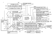
- FIG. 1 is a schematic block diagram of a digital single-lens reflex camera incorporating a strobe device which is a light emitting device according to an embodiment of the invention.
- FIG. 2A is a front perspective view of a camera body of the digital single-lens reflex camera incorporating the strobe device.
- FIG. 2B is a perspective view of the camera body, shown in FIG. 2A , in a state in which the strobe device is held up to a light emitting position.
- FIG. 3 is a schematic view of a strobe popup unit.
- FIG. 4 is a front view of the strobe device in a state held up to the light emitting position.
- FIG. 5A is a cross-sectional view taken on line A-A of FIG. 4
- FIG. 5B is a cross-sectional view taken on line B-B of FIG. 4 , each of which shows a case where a shielding member for protecting a soldered portion of an electrode part of a flash discharge tube is formed by a non-conductive elastic case.
- FIG. 6 is an enlarged view of an essential part of FIG. 5A .
- FIG. 7 is a cross-sectional view taken on line A-A of FIG. 4 .
- FIG. 8 is an enlarged view of an essential part of FIG. 7 , which shows a case where a strobe panel is integrally formed with a shielding part for protecting the soldered portion of the electrode part of the flash discharge tube.
- FIG. 1 is a schematic block diagram of a digital single-lens reflex camera incorporating a strobe device which is a light emitting device according to an embodiment of the invention.
- FIG. 2A is a front perspective view of a camera body 1 of the digital single-lens reflex camera incorporating the strobe device, in a state in which a lens unit 2 is removed therefrom
- FIG. 2B is a perspective view of the camera body 1 , shown in FIG. 2A , in a state in which the strobe device is held up to a light emitting position.
- the digital single-lens reflex camera for which the lens unit 2 is exchangeable will be described as an example of the image pickup apparatus of the invention, but this is not limitative.
- the digital single-lens reflex camera of the present embodiment has the lens unit 2 exchangeably provided on the front side (object side) of the camera body 1 shown in FIGS. 1, 2A, and 2B .
- Light having passed through the lens unit 2 forms an image on an image pickup unit 3 .
- the image pickup unit 3 which is implemented e.g. by a CCD sensor or a CMOS sensor, is held in the camera body 1 in a manner positionally adjustable at least in the optical axis direction of the lens unit 2 .
- a main mirror 5 Between the lens unit 2 and the image pickup unit 3 , there are arranged a main mirror 5 , a sub mirror 10 , and a shutter 6 .
- Light reflected from the main mirror 5 forms an image on a focus plate 7 and then is guided to an optical viewfinder 4 by a pentagonal prism 8 , while being partially guided to an exposure detection unit 9 .
- the main mirror 5 is formed as a half mirror, and part of light having passed through the main mirror 5 is reflected by the sub mirror 10 pivotally attached to the main mirror 5 , to enter a focus detection unit 11 .
- a release button 12 When a user half presses a release button 12 (SW 1 ), photometry by the exposure detection unit 9 , ranging by the focus detection unit 11 , and driving of a focus lens 14 by a lens drive unit 13 are started.
- the release button 12 When the user fully presses the release button 12 (SW 2 ), the main mirror 5 and the shutter 6 are driven, whereby light from the lens unit 2 enters the image pickup unit 3 .
- the image pickup unit 3 performs an exposure operation for starting a charge accumulation and charge reading operation.
- Analog image data output from the image pickup unit 3 is converted to digital image data by an analog-to-digital converter circuit 23 , and is subjected to predetermined image processing by an image processing circuit 24 , whereafter it is recorded and stored as a photographed image in a storage medium 16 mounted in an image recording and reading unit 15 .
- an image reproduction button 17 is pressed, the image stored in the storage medium 16 is displayed on a display device 18 .
- a system control circuit 19 controls the overall operation of the camera.
- the system control circuit 19 which is formed e.g. by a CPU or an MPU, controls the operations of respective circuits and so forth.
- the system control circuit 19 controls the lens drive unit 13 , based on an output from the focus detection unit 11 , to perform a focusing operation by driving the focus lens 14 in the optical axis direction.
- the system control circuit 19 cause an exposure control section 20 to control a diaphragm 21 of the lens unit 2 , the main mirror 5 , the shutter 6 , and a timing generator 22 .
- the timing generator 22 and the analog-to-digital converter circuit 23 are mounted on a mounting board 60 .
- the main mirror 5 is movable to a mirror-up position retracted from a photographic optical path
- the sub mirror 10 is also movable to the mirror-up position retracted from the photographic optical path by being folded onto the main mirror 5 .
- the shutter 6 has a front curtain and a rear curtain and controls transmission and blocking of a light flux from the lens unit 2 .
- the system control circuit 19 determines an aperture value and a shutter speed value according to an output from the exposure detection unit 9 and photographing conditions preset by the user.
- the system control circuit 19 causes the exposure control section 20 to control the diaphragm 21 to the determined aperture value. Further, the system control circuit 19 causes the exposure control section 20 to bring the main mirror 5 and the sub mirror 10 into the mirror-up position and control travel of the front and rear curtains of the shutter 6 according to the determined shutter speed value. Furthermore, the system control circuit 19 operates the exposure control section 20 to cause the timing generator 22 to output a pulse signal required for driving the image pickup unit 3 .
- the image pickup unit 3 performs a charge accumulation and charge reading operation according to the pulse signal output from the timing generator 22 .
- An electric charge read out from the image pickup unit 3 is converted to a digital value by the analog-to-digital converter circuit 23 and is sent as digital data to the image processing circuit 24 .
- the sent digital data is subjected to white balance adjustment, image compression processing, etc. by an image processing section 25 of the image processing circuit 24 , and then a recording control section 26 causes the image recording and reading unit 15 to store the processed data in the storage medium 16 as image data.
- the image reproduction button 17 When the image reproduction button 17 is pressed, the image data stored in the storage medium 16 is read into a display control section 27 of the image processing circuit 24 by the image recording and reading unit 15 , and is then converted to an analog image by a digital-to-analog converter circuit 28 to be displayed on the display device 18 .
- a photographing mode selection unit 29 as an operation member is capable of setting photographing modes, such as an automatic exposure mode, an aperture priority exposure mode (Av), a shutter-speed priority exposure mode (Tv), a manual mode (M), and a bulb mode (B).
- photographing modes such as an automatic exposure mode, an aperture priority exposure mode (Av), a shutter-speed priority exposure mode (Tv), a manual mode (M), and a bulb mode (B).
- a photographing mode selection unit 29 as an operation member is capable of setting photographing modes, such as an automatic exposure mode, an aperture priority exposure mode (Av), a shutter-speed priority exposure mode (Tv), a manual mode (M), and a bulb mode (B).
- Av aperture priority exposure mode
- Tv shutter-speed priority exposure mode
- M manual mode
- bulb mode B
- any of the aperture priority exposure mode (Av), the shutter-speed priority exposure mode (Tv), and the manual mode (M) it is possible to set the aperture value and the shutter speed value to respective desired values, as desired, using an aperture setting unit 31 and a shutter speed-setting unit 32 .
- the bulb mode when the release button 12 (SW 2 ) is pressed, photographing is started, and exposure is continued as long as the release button 12 (SW 2 ) is kept pressed. Then, when the release button 12 (SW 2 ) is released, the exposure is terminated, whereby the shutter speed can be determined during photographing.
- FIG. 3 is a schematic view of a strobe popup unit 34 .
- FIG. 4 is a front view of the strobe device 33 in a state held up to the light emitting position.
- FIG. 5A is a cross-sectional view taken on line A-A of FIG. 4
- FIG. 5B is a cross-sectional view taken on line B-B of FIG. 4 .
- FIG. 6 is an enlarged view of an essential part of FIG. 5A .
- the strobe popup unit 34 is configured to open and close the strobe device 33 .
- the strobe popup unit 34 is provided with a retaining lever 35 for retaining the strobe device 33 in a closed state (see FIG. 2A ).
- the retaining lever 35 is urged by a coil spring 36 in a direction in which the strobe device 33 is closed.
- the strobe popup unit 34 is provided with a solenoid 37 .
- the solenoid 37 is comprised of a permanent magnet, a coil, and a magnetic chip as a movable part. In a state in which the coil is not energized, the chip is retained by the magnetic force of the permanent magnet.
- the coil is energized to cancel out the magnetic force of the permanent magnet, whereby the chip is moved by the urging force of a coil spring 38 .
- the moved chip causes rotation of the retaining lever 35 to thereby release retainment of a strobe base 44 of the strobe device 33 .
- the strobe device 33 is brought up to the light emitting position by the urging force of a strobe-up spring 39 .
- the strobe base 44 functions as a base member in the invention.
- the system control circuit 19 causes the exposure control unit 20 to cause light emission of the strobe device 33 and exposure of the image pickup unit 3 by controlling the amount of light to be emitted from the strobe device 33 , the aperture value, and the shutter speed value, such that appropriate exposure is obtained. Further, in the automatic exposure mode, when it is determined by the exposure detection unit 9 that the luminance of an object is below a predetermined luminance, the system control circuit 19 automatically releases the retainment of the strobe base 44 of the strobe device 33 and brings the strobe device 33 up to the light emitting position. An operation for closing the strobe device 33 , i.e. moving the same to its accommodated position is manually performed by the user.
- the strobe device 33 includes a flash discharge tube 40 that emits light by being energized, a reflector 41 that reflects the light emitted from the flash discharge tube 40 toward an object, and a strobe panel 42 that scatters the reflected light.
- a portion of the strobe panel 42 through which light transmits has a Fresnel shape whereby light is substantially uniformly scattered toward a object.
- the strobe panel 42 functions as a panel member in the invention.
- Lead wires 45 a and 45 b are soldered to electrode parts 40 a provided at opposite ends of the flash discharge tube 40 , respectively.
- the lead wires 45 a and 45 b are connected to a capacitor, not shown.
- the flash discharge tube 40 has a trigger electrode 46 connected to a trigger capacitor, not shown.
- a trigger electrode 46 When causing the flash discharge tube 40 to emit light, xenon gas within the flash discharge tube 40 is ionized by an electric discharge from the trigger electrode 46 , whereby electric charge in the capacitor is discharged from the electrode parts 40 a of the flash discharge tube 40 to which the lead wires 45 a and 45 b are connected, to cause light emission.
- the flash discharge tube 40 is secured to the reflector 41 via an elastic member 43 .
- the reflector 41 is secured to the strobe panel 42 e.g. by bonding.
- the strobe panel 42 is held on the strobe base 44 by being secured to opposite ends 44 a and 44 b of the strobe base 44 by bonding and the like.
- the strobe base 44 has a strobe cover 47 attached thereto.
- the strobe cover 47 functions as a cover member in the invention.
- the strobe cover 47 is attached to the strobe base 44 such that it covers the flash discharge tube 40 , the reflector 41 , and the strobe panel 42 .
- the flash discharge tube 40 and the reflector 41 are disposed in a space surrounded by the strobe panel 42 , the strobe base 44 , and the strobe cover 47 .
- a gap 48 a is formed at an area where the strobe base 44 and the strobe cover 47 meet, and a gap 48 b is formed at an area where the strobe base 44 and the strobe panel 42 meet, as shown in FIG. 5A .
- non-conductive elastic cases 49 are provided on the respective electrode parts 40 a of the flash discharge tube 40 .
- Each elastic case 49 functions as a shielding member in the invention.
- the elastic case 49 is formed into a semi-cylindrical shape, using an elastic and heat-resistant material, such as silicone rubber.
- Each of the elastic cases 49 is fitted in grooves formed in the strobe panel 42 and the strobe base 44 , whereby it is secured to the strobe panel 42 and the strobe base 44 .
- the elastic case 49 is disposed such that the inner peripheral surface of the semi-cylindrical shape faces an associated one of the electrode parts 40 a of the flash discharge tube 40 so as to shield between the electrode part 40 a and an associated one of the gaps 48 a and 48 b .
- each of the elastic cases 49 is filled with a non-conductive elastic adhesive 50 to seal the electrode parts 40 a of the flash discharge tube 40 . This makes it possible to prevent invasion of static electricity from end openings of the respective elastic cases 49 .
- the elastic case 49 has a semi-cylindrical shape and elasticity, as described above, it is possible to easily assemble the elastic case 49 to the strobe panel 42 and the strobe base 44 in a state in which the flash discharge tube 40 having the lead wires soldered to the respective electrode parts 40 a thereof and the reflector 41 have been assembled to the strobe panel 42 .
- the elastic case 49 is formed of a heat-resistant material, it is also possible to solder the lead wires 45 a and 45 b to the respective electrode parts 40 a of the flash discharge tube 40 after the elastic cases 49 have been attached to the strobe panel 42 and the strobe base 44 .
- the elastic adhesive 50 is filled in a space inside the inner peripheral surface of the semi-cylindrical elastic case 49 , it is possible to easily control the elastic adhesive 50 to an appropriate amount. This makes it possible to uniformly maintain the thickness of the elastic adhesive 50 to thereby stabilize resistance to static electricity.
- An image pickup apparatus has the same construction as that of the digital single-lens reflex camera incorporating the strobe device according to the first embodiment described with reference to FIGS. 1 to 6 , except a shielding structure for protecting the soldered portions within the strobe device. Therefore, the same component elements are denoted by the same reference numerals, respectively, and description thereof is omitted. The following description is given of only different points from the first embodiment.
- the non-conductive elastic cases 49 formed as separate members from the strobe panel 42 are used as shielding members for shielding between the electrode parts 40 a of the flash discharge tube 40 and the respective gaps 48 a and 48 b.
- shielding parts 42 a integrally formed with the non-conductive strobe panel 42 are provided, without using separate members, as shielding members for protecting the soldered portions of the respective electrode parts 40 a of the flash discharge tube 40 .
- the shielding parts 42 a for protection of the respective soldered portions are integrally formed with the strobe panel 42 , it is possible not only to reduce the number of component parts to thereby reduce manufacturing costs, but also to simplify work for assembling the strobe panel 42 , the flash discharge tube 40 , the reflector 41 , the elastic member 43 , and the strobe base 44 .
- the elastic adhesive 50 is filled in a space inside the inner peripheral surface of the shielding parts 42 a of the strobe panel 42 , so that it is possible to easily control the elastic adhesive 50 to an appropriate amount, which makes it possible to uniformly maintain the thickness of the elastic adhesive 50 to thereby stabilize resistance to static electricity.
- the above-described first and second embodiments described above can each provide a mechanism which is excellent in assembly workability of the strobe device 33 and is capable of stably protecting soldered portions between the lead wires 45 a and 45 b and the respective electrode parts 40 a of the flash discharge tube 40 against static electricity.
Landscapes
- Engineering & Computer Science (AREA)
- Multimedia (AREA)
- Signal Processing (AREA)
- Stroboscope Apparatuses (AREA)
- Studio Devices (AREA)
- General Engineering & Computer Science (AREA)
- Led Device Packages (AREA)
Applications Claiming Priority (4)
| Application Number | Priority Date | Filing Date | Title |
|---|---|---|---|
| JP2013-209228 | 2013-10-04 | ||
| JP2013209228 | 2013-10-04 | ||
| JP2014179014A JP6494219B2 (ja) | 2013-10-04 | 2014-09-03 | 静電気からの保護機能を有する発光装置及び撮像装置 |
| JP2014-179014 | 2014-09-03 |
Publications (2)
| Publication Number | Publication Date |
|---|---|
| US20150098015A1 US20150098015A1 (en) | 2015-04-09 |
| US9438781B2 true US9438781B2 (en) | 2016-09-06 |
Family
ID=52776678
Family Applications (1)
| Application Number | Title | Priority Date | Filing Date |
|---|---|---|---|
| US14/503,658 Active 2034-10-04 US9438781B2 (en) | 2013-10-04 | 2014-10-01 | Light emitting device having function for protection against static electricity, and image pickup apparatus |
Country Status (5)
| Country | Link |
|---|---|
| US (1) | US9438781B2 (ru) |
| JP (1) | JP6494219B2 (ru) |
| KR (1) | KR20150040222A (ru) |
| CN (1) | CN104516172A (ru) |
| RU (1) | RU2014139662A (ru) |
Families Citing this family (2)
| Publication number | Priority date | Publication date | Assignee | Title |
|---|---|---|---|---|
| US10217946B2 (en) | 2014-03-17 | 2019-02-26 | Idemitsu Kosan Co., Ltd. | Dibenzofurans and dibenzothiophenes |
| JP6849839B2 (ja) * | 2020-03-03 | 2021-03-31 | 東芝テック株式会社 | 取引データ処理装置、プログラム及び取引データ処理方法 |
Citations (7)
| Publication number | Priority date | Publication date | Assignee | Title |
|---|---|---|---|---|
| US3855495A (en) * | 1973-11-05 | 1974-12-17 | Gte Sylvania Inc | Flash tube with insulator end cap |
| JPS6113544A (ja) | 1984-06-29 | 1986-01-21 | Fuji Xerox Co Ltd | フラツシユランプ |
| US20010051045A1 (en) * | 1998-01-28 | 2001-12-13 | Fuji Photo Film Co., Ltd. | Compact camera |
| JP2005063688A (ja) | 2003-08-12 | 2005-03-10 | Sanyo Electric Co Ltd | 端子部の絶縁及び保持用の部材 |
| US20070025719A1 (en) * | 2005-07-29 | 2007-02-01 | Fuji Photo Film Co., Ltd. | Flash light reducing plate and lens-fitted photo film unit |
| US20110182569A1 (en) * | 2010-01-28 | 2011-07-28 | Canon Kabushiki Kaisha | Imaging apparatus |
| US20110188848A1 (en) * | 2010-01-29 | 2011-08-04 | Canon Kabushiki Kaisha | Electronic flash device and image pickup apparatus provided with electronic flash device |
Family Cites Families (6)
| Publication number | Priority date | Publication date | Assignee | Title |
|---|---|---|---|---|
| JPH08129207A (ja) * | 1994-11-01 | 1996-05-21 | Olympus Optical Co Ltd | 閃光発光装置 |
| US5541688A (en) * | 1995-04-10 | 1996-07-30 | Eastman Kodak Company | Method of assembling flash unit to camera |
| JPH10260458A (ja) * | 1997-03-19 | 1998-09-29 | Canon Inc | 閃光発光装置およびこれを備えたカメラ |
| JP2000330167A (ja) * | 1999-05-24 | 2000-11-30 | Olympus Optical Co Ltd | カメラ用ストロボ装置 |
| JP2003091039A (ja) * | 2001-09-19 | 2003-03-28 | Canon Inc | 接写用ストロボ |
| JP2011221080A (ja) * | 2010-04-05 | 2011-11-04 | Ricoh Co Ltd | ストロボ装置および撮像装置 |
-
2014
- 2014-09-03 JP JP2014179014A patent/JP6494219B2/ja active Active
- 2014-09-29 CN CN201410514090.6A patent/CN104516172A/zh active Pending
- 2014-09-30 RU RU2014139662A patent/RU2014139662A/ru not_active Application Discontinuation
- 2014-10-01 KR KR20140132244A patent/KR20150040222A/ko not_active IP Right Cessation
- 2014-10-01 US US14/503,658 patent/US9438781B2/en active Active
Patent Citations (8)
| Publication number | Priority date | Publication date | Assignee | Title |
|---|---|---|---|---|
| US3855495A (en) * | 1973-11-05 | 1974-12-17 | Gte Sylvania Inc | Flash tube with insulator end cap |
| JPS6113544A (ja) | 1984-06-29 | 1986-01-21 | Fuji Xerox Co Ltd | フラツシユランプ |
| US20010051045A1 (en) * | 1998-01-28 | 2001-12-13 | Fuji Photo Film Co., Ltd. | Compact camera |
| JP2005063688A (ja) | 2003-08-12 | 2005-03-10 | Sanyo Electric Co Ltd | 端子部の絶縁及び保持用の部材 |
| US7108406B2 (en) | 2003-08-12 | 2006-09-19 | Sanyo Electric Co., Ltd. | Terminal retainer and strobe device using the retainer |
| US20070025719A1 (en) * | 2005-07-29 | 2007-02-01 | Fuji Photo Film Co., Ltd. | Flash light reducing plate and lens-fitted photo film unit |
| US20110182569A1 (en) * | 2010-01-28 | 2011-07-28 | Canon Kabushiki Kaisha | Imaging apparatus |
| US20110188848A1 (en) * | 2010-01-29 | 2011-08-04 | Canon Kabushiki Kaisha | Electronic flash device and image pickup apparatus provided with electronic flash device |
Also Published As
| Publication number | Publication date |
|---|---|
| KR20150040222A (ko) | 2015-04-14 |
| US20150098015A1 (en) | 2015-04-09 |
| RU2014139662A (ru) | 2016-04-20 |
| JP6494219B2 (ja) | 2019-04-03 |
| JP2015092230A (ja) | 2015-05-14 |
| CN104516172A (zh) | 2015-04-15 |
Similar Documents
| Publication | Publication Date | Title |
|---|---|---|
| JP2012182704A (ja) | 電子撮影装置 | |
| US8956060B2 (en) | Imaging apparatus | |
| US9609193B2 (en) | Compact interchangeable lens type camera | |
| US8408822B2 (en) | Camera | |
| US9438781B2 (en) | Light emitting device having function for protection against static electricity, and image pickup apparatus | |
| US10264167B2 (en) | Imaging apparatus | |
| JP5266950B2 (ja) | カメラ | |
| US8988583B2 (en) | Image-pickup apparatus and image-pickup system having light emitting member | |
| US9128355B2 (en) | Imaging apparatus | |
| US20070053678A1 (en) | Alarm systems for cameras | |
| JP2001249391A (ja) | 焦点インジケータを有する確認カメラおよび方法 | |
| JP2006050351A (ja) | 撮影装置 | |
| JP2008203630A (ja) | 撮像装置 | |
| JP2011114441A (ja) | 撮像装置 | |
| JP2013162194A (ja) | デジタルカメラの制御方法 | |
| JP2013162193A (ja) | デジタルカメラ | |
| JP2011250247A (ja) | 撮像装置 | |
| JP2018029329A (ja) | 撮像装置 | |
| JP5039496B2 (ja) | 撮像装置及びその制御方法 | |
| JP2007121427A (ja) | カメラ | |
| JP2004240025A (ja) | カメラ | |
| JP2010039163A (ja) | カメラ | |
| US20060216005A1 (en) | Lens-fitted photographic film unit | |
| JP2005115146A (ja) | ストロボ装置及びその制御方法、並びにカメラ | |
| JPH06233180A (ja) | 撮影装置 |
Legal Events
| Date | Code | Title | Description |
|---|---|---|---|
| AS | Assignment |
Owner name: CANON KABUSHIKI KAISHA, JAPAN Free format text: ASSIGNMENT OF ASSIGNORS INTEREST;ASSIGNORS:UEDA, HARUHISA;OYA, SOICHIRO;REEL/FRAME:035603/0030 Effective date: 20141024 |
|
| STCF | Information on status: patent grant |
Free format text: PATENTED CASE |
|
| MAFP | Maintenance fee payment |
Free format text: PAYMENT OF MAINTENANCE FEE, 4TH YEAR, LARGE ENTITY (ORIGINAL EVENT CODE: M1551); ENTITY STATUS OF PATENT OWNER: LARGE ENTITY Year of fee payment: 4 |
|
| FEPP | Fee payment procedure |
Free format text: MAINTENANCE FEE REMINDER MAILED (ORIGINAL EVENT CODE: REM.); ENTITY STATUS OF PATENT OWNER: LARGE ENTITY |