US9437726B2 - Field effect transistor - Google Patents
Field effect transistor Download PDFInfo
- Publication number
- US9437726B2 US9437726B2 US14/787,443 US201414787443A US9437726B2 US 9437726 B2 US9437726 B2 US 9437726B2 US 201414787443 A US201414787443 A US 201414787443A US 9437726 B2 US9437726 B2 US 9437726B2
- Authority
- US
- United States
- Prior art keywords
- layer
- high resistance
- carbon concentration
- side closer
- less
- Prior art date
- Legal status (The legal status is an assumption and is not a legal conclusion. Google has not performed a legal analysis and makes no representation as to the accuracy of the status listed.)
- Active
Links
Images



Classifications
-
- H01L29/7787—
-
- H—ELECTRICITY
- H10—SEMICONDUCTOR DEVICES; ELECTRIC SOLID-STATE DEVICES NOT OTHERWISE PROVIDED FOR
- H10D—INORGANIC ELECTRIC SEMICONDUCTOR DEVICES
- H10D30/00—Field-effect transistors [FET]
- H10D30/40—FETs having zero-dimensional [0D], one-dimensional [1D] or two-dimensional [2D] charge carrier gas channels
- H10D30/47—FETs having zero-dimensional [0D], one-dimensional [1D] or two-dimensional [2D] charge carrier gas channels having two-dimensional [2D] charge carrier gas channels, e.g. nanoribbon FETs or high electron mobility transistors [HEMT]
- H10D30/471—High electron mobility transistors [HEMT] or high hole mobility transistors [HHMT]
- H10D30/475—High electron mobility transistors [HEMT] or high hole mobility transistors [HHMT] having wider bandgap layer formed on top of lower bandgap active layer, e.g. undoped barrier HEMTs such as i-AlGaN/GaN HEMTs
- H10D30/4755—High electron mobility transistors [HEMT] or high hole mobility transistors [HHMT] having wider bandgap layer formed on top of lower bandgap active layer, e.g. undoped barrier HEMTs such as i-AlGaN/GaN HEMTs having wide bandgap charge-carrier supplying layers, e.g. modulation doped HEMTs such as n-AlGaAs/GaAs HEMTs
-
- H01L29/1029—
-
- H01L29/205—
-
- H01L29/207—
-
- H01L29/7786—
-
- H—ELECTRICITY
- H10—SEMICONDUCTOR DEVICES; ELECTRIC SOLID-STATE DEVICES NOT OTHERWISE PROVIDED FOR
- H10D—INORGANIC ELECTRIC SEMICONDUCTOR DEVICES
- H10D30/00—Field-effect transistors [FET]
- H10D30/40—FETs having zero-dimensional [0D], one-dimensional [1D] or two-dimensional [2D] charge carrier gas channels
- H10D30/47—FETs having zero-dimensional [0D], one-dimensional [1D] or two-dimensional [2D] charge carrier gas channels having two-dimensional [2D] charge carrier gas channels, e.g. nanoribbon FETs or high electron mobility transistors [HEMT]
- H10D30/471—High electron mobility transistors [HEMT] or high hole mobility transistors [HHMT]
- H10D30/475—High electron mobility transistors [HEMT] or high hole mobility transistors [HHMT] having wider bandgap layer formed on top of lower bandgap active layer, e.g. undoped barrier HEMTs such as i-AlGaN/GaN HEMTs
-
- H—ELECTRICITY
- H10—SEMICONDUCTOR DEVICES; ELECTRIC SOLID-STATE DEVICES NOT OTHERWISE PROVIDED FOR
- H10D—INORGANIC ELECTRIC SEMICONDUCTOR DEVICES
- H10D62/00—Semiconductor bodies, or regions thereof, of devices having potential barriers
- H10D62/10—Shapes, relative sizes or dispositions of the regions of the semiconductor bodies; Shapes of the semiconductor bodies
- H10D62/17—Semiconductor regions connected to electrodes not carrying current to be rectified, amplified or switched, e.g. channel regions
- H10D62/213—Channel regions of field-effect devices
- H10D62/221—Channel regions of field-effect devices of FETs
-
- H—ELECTRICITY
- H10—SEMICONDUCTOR DEVICES; ELECTRIC SOLID-STATE DEVICES NOT OTHERWISE PROVIDED FOR
- H10D—INORGANIC ELECTRIC SEMICONDUCTOR DEVICES
- H10D62/00—Semiconductor bodies, or regions thereof, of devices having potential barriers
- H10D62/80—Semiconductor bodies, or regions thereof, of devices having potential barriers characterised by the materials
- H10D62/82—Heterojunctions
- H10D62/824—Heterojunctions comprising only Group III-V materials heterojunctions, e.g. GaN/AlGaN heterojunctions
-
- H—ELECTRICITY
- H10—SEMICONDUCTOR DEVICES; ELECTRIC SOLID-STATE DEVICES NOT OTHERWISE PROVIDED FOR
- H10D—INORGANIC ELECTRIC SEMICONDUCTOR DEVICES
- H10D62/00—Semiconductor bodies, or regions thereof, of devices having potential barriers
- H10D62/80—Semiconductor bodies, or regions thereof, of devices having potential barriers characterised by the materials
- H10D62/85—Semiconductor bodies, or regions thereof, of devices having potential barriers characterised by the materials being Group III-V materials, e.g. GaAs
- H10D62/854—Semiconductor bodies, or regions thereof, of devices having potential barriers characterised by the materials being Group III-V materials, e.g. GaAs further characterised by the dopants
-
- H01L29/1079—
-
- H01L29/2003—
-
- H01L29/41766—
-
- H01L29/518—
-
- H—ELECTRICITY
- H10—SEMICONDUCTOR DEVICES; ELECTRIC SOLID-STATE DEVICES NOT OTHERWISE PROVIDED FOR
- H10D—INORGANIC ELECTRIC SEMICONDUCTOR DEVICES
- H10D62/00—Semiconductor bodies, or regions thereof, of devices having potential barriers
- H10D62/10—Shapes, relative sizes or dispositions of the regions of the semiconductor bodies; Shapes of the semiconductor bodies
- H10D62/17—Semiconductor regions connected to electrodes not carrying current to be rectified, amplified or switched, e.g. channel regions
- H10D62/351—Substrate regions of field-effect devices
- H10D62/357—Substrate regions of field-effect devices of FETs
- H10D62/364—Substrate regions of field-effect devices of FETs of IGFETs
-
- H—ELECTRICITY
- H10—SEMICONDUCTOR DEVICES; ELECTRIC SOLID-STATE DEVICES NOT OTHERWISE PROVIDED FOR
- H10D—INORGANIC ELECTRIC SEMICONDUCTOR DEVICES
- H10D62/00—Semiconductor bodies, or regions thereof, of devices having potential barriers
- H10D62/80—Semiconductor bodies, or regions thereof, of devices having potential barriers characterised by the materials
- H10D62/85—Semiconductor bodies, or regions thereof, of devices having potential barriers characterised by the materials being Group III-V materials, e.g. GaAs
- H10D62/8503—Nitride Group III-V materials, e.g. AlN or GaN
-
- H—ELECTRICITY
- H10—SEMICONDUCTOR DEVICES; ELECTRIC SOLID-STATE DEVICES NOT OTHERWISE PROVIDED FOR
- H10D—INORGANIC ELECTRIC SEMICONDUCTOR DEVICES
- H10D64/00—Electrodes of devices having potential barriers
- H10D64/20—Electrodes characterised by their shapes, relative sizes or dispositions
- H10D64/23—Electrodes carrying the current to be rectified, amplified, oscillated or switched, e.g. sources, drains, anodes or cathodes
- H10D64/251—Source or drain electrodes for field-effect devices
- H10D64/256—Source or drain electrodes for field-effect devices for lateral devices wherein the source or drain electrodes are recessed in semiconductor bodies
-
- H—ELECTRICITY
- H10—SEMICONDUCTOR DEVICES; ELECTRIC SOLID-STATE DEVICES NOT OTHERWISE PROVIDED FOR
- H10D—INORGANIC ELECTRIC SEMICONDUCTOR DEVICES
- H10D64/00—Electrodes of devices having potential barriers
- H10D64/60—Electrodes characterised by their materials
- H10D64/66—Electrodes having a conductor capacitively coupled to a semiconductor by an insulator, e.g. MIS electrodes
- H10D64/68—Electrodes having a conductor capacitively coupled to a semiconductor by an insulator, e.g. MIS electrodes characterised by the insulator, e.g. by the gate insulator
- H10D64/693—Electrodes having a conductor capacitively coupled to a semiconductor by an insulator, e.g. MIS electrodes characterised by the insulator, e.g. by the gate insulator the insulator comprising nitrogen, e.g. nitrides, oxynitrides or nitrogen-doped materials
Definitions
- the present invention relates to a field effect transistor.
- a nitride semiconductor is featured in having a high breakdown voltage and high carrier mobility, utilization of the nitride semiconductor as a power device, etc. is expected.
- a field effect transistor used in a power device, etc. and made of a nitride semiconductor is demanded to have high reliability particularly in an off-state where a high voltage is applied, namely to have a long lifetime.
- One example of related-art field effect transistors has a structure in which a substrate withstand voltage is improved with control of a carbon concentration in a GaN substrate, as disclosed in Japanese Unexamined Patent Application Publication No. 2010-245504 (PTL 1).
- PTL 1 does not include any discussions about an improvement of lifetime in the actual transistor operation.
- the related-art field effect transistor mentioned above has the problem that there is still a room for the improvement of lifetime and reliability is not increased sufficiently.
- an object of the present invention is to provide a field effect transistor having sufficiently high reliability.
- the present invention provides a field effect transistor comprising:
- a source electrode and a drain electrode disposed on the nitride semiconductor layer at positions spaced from each other;
- a gate electrode formed between the source electrode and the drain electrode and on the nitride semiconductor layer, the gate electrode being connected to the nitride semiconductor layer directly or with an insulating film interposed therebetween,
- a carbon concentration in the buffer layer at side closer to the high resistance layer is not less than 0.8 ⁇ 10 19 /cm 3 and not more than 1.0 ⁇ 10 21 /cm 3 ,
- a carbon concentration in the high resistance layer at side closer to the buffer layer is not less than 3.7 ⁇ 10 18 /cm 3 and not more than 1.0 ⁇ 10 21 /cm 3 , and
- a carbon concentration in the high resistance layer at side closer to the channel layer is not less than 1.4 ⁇ 10 19 /cm 3 and not more than 1.0 ⁇ 10 21 /cm 3 .
- the nitride semiconductor layer may be expressed by Al x In y Ga 1-x-y N (x ⁇ 0, y ⁇ 0, and 0 ⁇ x+y ⁇ 1).
- the carbon concentration in the buffer layer at the side closer to the high resistance layer means the carbon concentration in a part of the buffer layer at the side closer to the high resistance layer than a midpoint of the buffer layer in a direction of layer thickness.
- the carbon concentration in the high resistance layer at the side closer to the buffer layer means the carbon concentration in a part of the high resistance layer at the side closer to the buffer layer than a midpoint of the high resistance layer in a direction of layer thickness.
- the carbon concentration in the high resistance layer at the side closer to the channel layer means the carbon concentration in a part of the high resistance layer at the side closer to the channel layer than the midpoint of the high resistance layer in the direction of layer thickness.
- the carbon concentration in the buffer layer at the side closer to the high resistance layer is not less than 1.2 ⁇ 10 19 /cm 3 ,
- the carbon concentration in the high resistance layer at the side closer to the buffer layer is not less than 4.4 ⁇ 10 18 /cm 3 .
- the carbon concentration in the high resistance layer at the side closer to the channel layer is not less than 1.6 ⁇ 10 19 /cm 3 .
- the carbon concentration in the buffer layer at the side closer to the high resistance layer is not less than 1.6 ⁇ 10 19 /cm 3 ,
- the carbon concentration in the high resistance layer at the side closer to the buffer layer is not less than 5.4 ⁇ 10 18 /cm 3 .
- the carbon concentration in the high resistance layer at the side closer to the channel layer is not less than 1.9 ⁇ 10 19 /cm 3 .
- the carbon concentration in the high resistance layer gradually increases toward the channel layer from the side close to the buffer layer.
- the field effect transistor of the present invention includes a substrate, a buffer layer laminated on the substrate, a high resistance layer laminated on the buffer layer, a channel layer laminated on the high resistance layer, and a nitride semiconductor layer laminated on the channel layer and serving as a barrier layer.
- a carbon concentration in the buffer layer at the side closer to the high resistance layer is not less than 0.8 ⁇ 10 19 /cm 3 and not more than 1.0 ⁇ 10 21 /cm 3 .
- a carbon concentration in the high resistance layer at the side closer to the buffer layer is not less than 3.7 ⁇ 10 18 /cm 3 and not more than 1.0 ⁇ 10 21 /cm 3 .
- a carbon concentration in the high resistance layer at the side closer to the channel layer is not less than 1.4 ⁇ 10 19 /cm 3 and not more than 1.0 ⁇ 10 21 /cm 3 . As a result, a lifetime can be prolonged drastically. Hence reliability can be increased sufficiently.
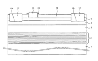
- FIG. 1 is a schematic sectional view of a field effect transistor according to one embodiment of the present invention.
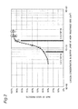
- FIG. 2 is a graph related to a carbon concentration in a buffer layer at the side closer to a high resistance layer.
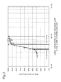
- FIG. 3 is a graph related to a carbon concentration in the high resistance layer at the side closer to the buffer layer.
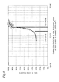
- FIG. 4 is a graph related to a carbon concentration in the high resistance layer at the side closer to a channel layer.
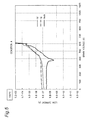
- FIG. 5 is a graph depicting a relation between a leak current and a drain voltage in a transistor under a condition A.
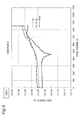
- FIG. 6 is a graph depicting a relation between a leak current and a drain voltage in the transistor under a condition B.
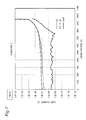
- FIG. 7 is a graph depicting a relation between a leak current and a drain voltage in the transistor under a condition C.
- FIG. 8 is a graph depicting a relation between a leak current and a drain voltage in the transistor under a condition D.
- FIG. 9A is a graph depicting a relation between a carbon concentration in the high resistance layer at the side closer to the buffer layer and an Isub reverse voltage.
- FIG. 9B is a graph depicting a relation between the carbon concentration in the high resistance layer at the side closer to the channel layer and an Isub reverse voltage.
- FIG. 9C is a graph depicting a relation between a carbon concentration in the buffer layer at the side closer to the high resistance layer and an Isub reverse voltage.
- a field effect transistor of the present invention will be described in detail below in connection with an illustrated embodiment.
- FIG. 1 is a schematic sectional view of a field effect transistor according to one embodiment of the present invention, the view being taken along a plane perpendicular to a direction of layer thickness of the transistor.
- the field effect transistor of the present invention includes a substrate 1 that is a silicon substrate, a buffer layer 2 laminated on the substrate 1 , a high resistance layer 3 laminated on the buffer layer 2 , a channel layer 4 laminated on the high resistance layer 3 , a barrier layer 5 laminated on the channel layer 4 , a source electrode 11 and a drain electrode 12 that are disposed on the barrier layer 5 at positions spaced from each other, and a gate electrode 13 that is formed between the source electrode 11 and the drain electrode 12 and on the barrier layer 5 .
- a first insulating film 20 is formed between the barrier layer 5 and the gate electrode 13 .
- a second insulating film 21 covers an almost entire region of an upper surface of the barrier layer 5 where the barrier layer 5 is not covered with the source electrode 11 and the drain electrode 12 .
- the barrier layer 5 is one example of a nitride semiconductor layer.
- the buffer layer 2 is constituted by plural films of AlN and plural films of Al x Ga 1-x N (0 ⁇ x ⁇ 1). More specifically, the buffer layer 2 has a superlattice structure in which AlN and Al x Ga 1-x N are alternately laminated.
- An Al composition x of Al x Ga 1-x N is constant in a depth direction.
- a total layer thickness of the plural films of AlN and the plural films of Al x Ga 1-x N, i.e., a layer thickness of the buffer layer 2 is 2.3 ⁇ m.
- a main purpose of the buffer layer 2 is to ensure a withstand voltage across a region from the barrier layer 5 to the substrate 1 .
- the buffer layer 2 is formed such that a carbon concentration in the buffer layer 2 at the side closer to the high resistance layer 3 is not less than 0.8 ⁇ 10 19 /cm 3 , desirably not less than 1.6 ⁇ 10 19 /cm 3 , and not more than 1.0 ⁇ 10 21 /cm 3 . If the carbon concentration in the buffer layer 2 at the side closer to the high resistance layer 3 is more than 1.0 ⁇ 10 21 /cm 3 , crystallinity would deteriorate, and a side effect, e.g., a decrease of the withstand voltage or an increase of a leak, would start to occur.
- the high resistance layer 3 is a GaN layer having a high carbon concentration and having a layer thickness of 840 nm.
- a main purpose of the high resistance layer 3 is to reduce a leak between the source and the drain via a portion that is positioned under the channel layer 4 .
- electric resistance of the high resistance layer 3 is set to be higher than that of the channel layer 4 .
- a carbon concentration is not less than 3.7 ⁇ 10 18 /cm 3 , desirably not less than 5.4 ⁇ 10 18 /cm 3 , and not more than 1.0 ⁇ 10 21 /cm 3 over an entire region in the depth direction thereof.
- a carbon concentration in the high resistance layer 3 at the side closer to the channel layer 4 is not less than 1.4 ⁇ 10 19 /cm 3 , desirably not less than 1.9 ⁇ 10 19 /cm 3 , and not more than 1.0 ⁇ 10 21 /cm 3 . If the carbon concentration in the high resistance layer 3 at the side closer to the channel layer 4 is more than 1.0 ⁇ 10 21 /cm 3 , crystallinity would deteriorate, and a side effect, e.g., a decrease of the withstand voltage or an increase of a leak, would start to occur.
- the carbon concentration in the high resistance layer 3 in the depth direction gradually increases toward the channel layer 4 from the side close to the buffer layer 2 .
- Such a feature is effective in causing carrier compensation due to a lattice mismatch between the superlattice buffer layer and the GaN layer, and in improving reliability.
- the channel layer 4 is made of GaN having a small carbon concentration, and it has a layer thickness of 800 nm.
- the carbon concentration in the channel layer 4 is to be as small as possible and is desirably not more than 1 ⁇ 10 17 /cm 3 . If the carbon concentration in the channel layer 4 is high, a collapse phenomenon that the on-resistance during a high-voltage operation becomes higher than the on-resistance during a low-voltage operation in the field effect transistor structure would be more likely to occur.
- the barrier layer 5 is made of AlGaN with an Al mixed ratio of about 17%, and it has a layer thickness of 34 nm.
- the barrier layer 5 and the channel layer 4 form a hetero junction.
- 2DEG two dimensional electron gas
- the source electrode 11 and the drain electrode 12 are ohmic-connected to the 2DEG in the channel layer 4 . More specifically, grooves 4 a and 4 b called “recesses” are formed in an upper surface of the channel layer 4 , and the grooves 4 a and 4 b are filled with respective parts of the source electrode 11 and the drain electrode 12 . With such a structure, the source electrode 11 and the drain electrode 12 are each contacted with the 2DEG from a horizontal direction.
- the first insulating film 20 is formed under the gate electrode 13 .
- the gate electrode 13 is formed on the barrier layer 5 with the first insulating film 20 interposed therebetween.
- a distance between the gate electrode 13 and the drain electrode 12 is 15 ⁇ m, and a distance between the gate electrode 13 and the source electrode 11 is 2 ⁇ m.
- a gate length is 2 ⁇ m, and a gate width is about 160 mm.
- the gate length corresponds to a length of the gate electrode 13 in a right and left direction on the drawing sheet of FIG. 1 .
- the gate width corresponds to a length of the gate electrode 13 in a direction perpendicular to the drawing sheet of FIG. 1 .
- the first insulating film 20 is made of Si-rich SiN.
- the first insulating film 20 is formed to be further positioned over a lateral surface of the gate electrode 13 at the side closer to the source electrode 11 and over a lateral surface of the gate electrode 13 at the side closer to the drain electrode 12 .
- a part of the first insulating film 20 is formed on the second insulating film 21 .
- the second insulating film 21 is made of SiN as per stoichiometry.
- the second insulating film 21 is formed in regions other than the regions where the source electrode 11 , the drain electrode 12 , and the first insulating film 20 are formed. Thus, the second insulating film 21 covers a most part of the upper surface of the barrier layer 5 .
- FIG. 2 is a graph depicting a relation between the carbon concentration in the buffer layer 2 at the side closer to the high resistance layer 3 and the rate of good products.
- Scale markings denoted by 1E+18, 1E+19, and 1E+20 along a horizontal axis of FIG. 2 represent 10 18 , 10 19 , and 10 20 , respectively.
- 0.8 ⁇ 10 ⁇ 19 represents 0.8 ⁇ 10 19 and corresponds to the carbon concentration at an intersection between a thick linear line on the left and the horizontal axis.
- 1.6 ⁇ 10 ⁇ 19 represents 1.6 ⁇ 10 19 and corresponds to the carbon concentration at an intersection between a thick linear line on the right and the horizontal axis.
- the rate of good products starts to drastically increase from a point at which the carbon concentration in the buffer layer 2 at the side closer to the high resistance layer 3 reaches and exceeds 0.8 ⁇ 10 19 /cm 3 .
- the rate of good products is 90% or more.
- a high rate of good products is stably obtained at the carbon concentration of not less than 1.6 ⁇ 10 19 /cm 3 .
- the carbon concentration in the high resistance layer 3 at the side closer to the buffer layer 2 is not less than 3.7 ⁇ 10 18 /cm 3 and not more than 1.0 ⁇ 10 21 /cm 3
- the carbon concentration in the high resistance layer 3 at the side closer to the channel layer 4 is not less than 1.4 ⁇ 10 19 /cm 3 and not more than 1.0 ⁇ 10 21 /cm 3 .
- the carbon concentration is maximized in its surface at the side close to the channel layer 4 .
- the carbon concentration gradually increases toward the channel layer 4 from the side close to the buffer layer 2 .
- FIG. 3 is a graph depicting a relation between the carbon concentration in the high resistance layer 3 at the side closer to the buffer layer 2 and the rate of good products.
- Scale markings denoted by 1E+18, 1E+19, and 1E+20 along a horizontal axis of FIG. 3 represent 10 18 , 10 19 , and 10 20 , respectively.
- 3.7 ⁇ 10 ⁇ 18 represents 3.7 ⁇ 10 18 and corresponds to the carbon concentration at an intersection between a thick linear line on the left and the horizontal axis.
- 5.4 ⁇ 10 ⁇ 18 represents 5.4 ⁇ 10 18 and corresponds to the carbon concentration at an intersection between a thick linear line on the right and the horizontal axis.
- the rate of good products starts to drastically increase from a point at which the carbon concentration in the high resistance layer 3 at the side closer to the buffer layer 2 reaches and exceeds 3.7 ⁇ 10 18 /cm 3 .
- the rate of good products is 90% or more.
- a high rate of good products is stably obtained at the carbon concentration of not less than 5.4 ⁇ 10 18 /cm 3 .
- the carbon concentration in the buffer layer 2 at the side closer to the high resistance layer 3 is set to be not less than 0.8 ⁇ 10 19 /cm 3 and not more than 1.0 ⁇ 10 21 /cm 3
- the carbon concentration in the high resistance layer 3 at the side closer to the channel layer 4 is set to be not less than 1.4 ⁇ 10 19 /cm 3 and not more than 1.0 ⁇ 10 21 /cm 3 .
- FIG. 4 is a graph depicting a relation between the carbon concentration in the high resistance layer 3 at the side closer to the channel layer 4 and the rate of good products.
- Scale markings denoted by 1E+18, 1E+19, and 1E+20 along a horizontal axis of FIG. 4 represent 10 18 , 10 19 , and 10 20 , respectively.
- 1.4 ⁇ 10 ⁇ 19 represents 1.4 ⁇ 10 19 and corresponds to the carbon concentration at an intersection between a thick linear line on the left and the horizontal axis.
- 1.9 ⁇ 10 ⁇ 19 represents 1.9 ⁇ 10 19 and corresponds to the carbon concentration at an intersection between a thick linear line on the right and the horizontal axis.
- the rate of good products starts to drastically increase from a point at which the carbon concentration in the high resistance layer 3 at the side closer to the channel layer 4 reaches and exceeds 1.4 ⁇ 10 19 /cm 3 .
- the rate of good products is 90% or more.
- a high rate of good products is stably obtained at the carbon concentration of not less than 1.9 ⁇ 10 19 /cm 3 .
- the carbon concentration in the buffer layer 2 at the side closer to the high resistance layer 3 is set to be not less than 0.8 ⁇ 10 19 /cm 3 and not more than 1.0 ⁇ 10 21 /cm 3
- the carbon concentration in the high resistance layer 3 at the side closer to the buffer layer 2 is set to be not less than 3.7 ⁇ 10 18 /cm 3 and not more than 1.0 ⁇ 10 21 /cm 3 .
- the lifetime can be drastically prolonged by setting the carbon concentration in the buffer layer 2 at the side closer to the high resistance layer 3 to be not less than 0.8 ⁇ 10 19 /cm 3 and not more than 1.0 ⁇ 10 21 /cm 3 in comparison with the case of setting the carbon concentration in the buffer layer 2 at the side closer to the high resistance layer 3 to be less than 0.8 ⁇ 10 19 /cm 3 or more than 1.0 ⁇ 10 21 /cm 3 . Accordingly, reliability can be increased sufficiently.
- the inventors have found that, in the transistor structure, generation of a leak current flowing from the drain electrode toward the rear surface of the substrate results in reduction of reliability.
- FIGS. 5 to 8 are each a graph depicting a relation between a leak current and a drain voltage in a transistor when measured in an environment of 150° C.
- the transistor is a field effect transistor having the same configuration as that of the field effect transistor illustrated in FIG. 1 .
- the leak currents depicted in FIGS. 5 to 8 are each measured under conditions that the gate voltage is set to ⁇ 10 V, and the source voltage and the voltage at the rear surface of the substrate are both set to 0 V. Moreover, in FIGS. 5 to 8 , the leak current flowing in the drain electrode is denoted by Id, the leak current flowing in the gate electrode is denoted by Ig, and the leak current flowing in the rear surface of the substrate is denoted by Isub.
- a vertical axis is graduated in log scale, and the leak current is indicated as an absolute value.
- Isub flows in a direction toward the drain electrode from the rear surface of the substrate.
- the direction of Isub is changed over.
- Isub flows in a direction toward the rear surface of the substrate from the drain electrode.
- the drain voltage at which the flowing direction of Isub is reversed i.e., the Isub reverse voltage
- Conditions A to D set in the cases of FIGS. 5 to 8 are as per indicated in Table given below.
- FIGS. 9A to 9C are each a graph depicting a relation between the carbon concentration and the Isub reverse voltage. It is to be noted that the Isub reverse voltages in FIGS. 9A to 9C have been measured by changing the carbon concentration not only in respective ranges indicated along horizontal axes, but also in ranges other than the indicated ranges of the carbon concentration.
- the Isub reverse voltages tend to increase in any regions of the carbon concentrations along the horizontal axes at a higher carbon concentration.
- the substrate 1 is a silicon substrate, it may be, instead of the silicon substrate, another type of substrate on which a nitride semiconductor can be laminated.
- a sapphire substrate, a GaN substrate, a SiC substrate, or an AlN substrate may be used in the embodiment.
- the buffer layer 2 is made of AlN and Al x Ga 1-x N
- the buffer layer 2 may be made of, instead of AlN and Al x Ga 1-x N, one or more materials insofar as the materials satisfy the withstand voltage required for the nitride semiconductor.
- the Al composition x of Al x Ga 1-x N in the buffer layer 2 is constant in the depth direction, it may be gradually changed in the depth direction.
- a composition gradient layer containing Al x Ga 1-x N with the Al composition x of Al x Ga 1-x N being gradually changed in the depth direction may be used as another example of the buffer layer in the above embodiment.
- the buffer layer 2 may be replaced with a buffer layer having a multilayer structure in which a single layer or plural layers of Al x Ga 1-x N and a single layer or plural layers of Al y Ga 1-y N (0 ⁇ x ⁇ 1, 0 ⁇ y ⁇ 1, and x ⁇ y) are laminated.
- the buffer layer 2 may be replaced with a buffer layer in combination of the above-mentioned composition gradient layer and the above-mentioned multilayer structure.
- an underlying layer to promote crystal growth may be disposed between the buffer layer 2 and the substrate 1 .
- the underlying layer is made of AlN or GaN, for example.
- the second insulating film 21 covers the almost entire region of the upper surface of the barrier layer 5 where the barrier layer 5 is not covered with the source electrode and the drain electrode, the second insulating film 21 may cover a part or the whole of the relevant region.
- the carbon concentration in the high resistance layer 3 at the side closer to the buffer layer 2 is preferably not less than 3.7 ⁇ 10 18 /cm 3 , desirably not less than 5.4 ⁇ 10 18 /cm 3 , and not more than 1.0 ⁇ 10 21 /cm 3 over the entire region of the high resistance layer 3 in the depth direction.
- the source electrode 11 and the drain electrode 12 are partly buried in the grooves 4 a and 4 b , respectively, the entireties of those electrodes may be not buried in the grooves 4 a and 4 b.
- the A1 mixed ratio in the barrier layer 5 is about 17%, it may be set to a value other than about 17% insofar as 2DEG (two dimensional electron gas) is generated in a portion of the channel layer 4 at or near the interface between the barrier layer 5 and the channel layer 4 .
- 2DEG two dimensional electron gas
- AlN may be formed between the barrier layer 5 and the channel layer 4 .
- a GaN layer may be formed as one example of a cap layer on the barrier layer 5 .
- the cap layer is effective in preventing oxidation of Al in AlGaN in the barrier layer 5 , preventing intrusion of impurities, and preventing distortion of the barrier layer, which is caused due to a difference in the lattice constant, by sandwiching the barrier layer 5 made of AlGaN with the two GaN layers from both the sides.
- the source electrode 11 and the drain electrode 12 are ohmic-connected to the 2DEG by forming the recesses where those electrodes are disposed, the recesses are not always required to be used insofar as those electrodes are ohmic-connected to the 2DEG.
- the source electrode 11 and the drain electrode 12 may be conducted to the 2DEG, for example, by injecting ions into respective regions of the channel layer 4 positioned under the source electrode 11 and the drain electrode 12 .
- the source electrode 11 and the drain electrode 12 may be conducted to the 2DEG by performing high-temperature annealing such that the metals of the source electrode 11 and the drain electrode 12 are permeated into the respective regions of the channel layer 4 positioned under the source electrode 11 and the drain electrode 12 .
- the gate electrode 13 is formed on the barrier layer 5 with the first insulating film 20 interposed between them, the gate electrode 13 may be formed directly on the barrier layer 5 .
- the gate electrode 13 may be formed directly on the surface of the nitride semiconductor insofar as the gate 13 is operable to turn on/off the field effect transistor.
- the first insulating film 20 is made of Si-rich SiN
- the first insulating film 20 may be made of, instead of Si-rich SiN, another material insofar as the material can reduce a leak between the gate electrode 13 and the nitride semiconductor.
- the second insulating film 21 is made of SiN as per stoichiometry
- the second insulating film 21 may be made of a different material (e.g., SiO 2 ) other than SiN insofar as the material can ensure insulation between the gate electrode 13 and the source electrode 11 , insulation between the gate electrode 13 and the drain electrode 12 , and insulation between the source electrode 11 and the drain electrode 12 .
- the second insulating film 21 is made of SiN formed as per stoichiometry on the barrier layer 5
- the second insulating film 21 may be made of a Si-rich SiN film formed on the barrier layer 5 , and of an insulating film made of a material other than SiN and formed on the SiN film.
- the second insulating film 21 having a single-layer structure may be replaced with a second insulating film having a multilayer structure.
- the relevant distance may be set to be shorter than 15 ⁇ m or longer than 15 ⁇ m insofar as the distance is within a range capable of maintaining the withstand voltage between the gate and the drain, and insofar as a leak is not increased excessively.
- the relevant distance is desirably set to, e.g., 5 ⁇ m or more.
- the relevant distance between the gate electrode 13 and the source electrode 11 is set to 2 ⁇ m
- the relevant distance may be set shorter than 2 ⁇ m or longer than 2 ⁇ m insofar as the distance is within a range capable of maintaining the withstand voltage between the gate and the source, and insofar as a leak is not increased excessively.
- the relevant distance is desirably set to, e.g., 0.1 ⁇ m or more.
- the gate length is set to 2 ⁇ m
- the gate length may be set to be shorter than 2 ⁇ m or longer than 2 ⁇ m insofar as a leak is not increased excessively due to a short channel effect.
- the gate length is desirably set to, e.g., 0.5 ⁇ m or more.
- the gate width is set to about 160 mm
- the value of about 160 mm is set to obtain the desired on-resistance. Accordingly, the gate width may be set to be longer than 160 mm or shorter than 160 mm. Thus, the gate width can be set optionally.
- a source electrode 11 and a drain electrode 12 disposed on the nitride semiconductor layer 5 at positions spaced from each other;
- a gate electrode 13 formed between the source electrode 11 and the drain electrode 12 and on the nitride semiconductor layer 5 , the gate electrode being connected to the nitride semiconductor layer 5 directly or with an insulating film 20 interposed therebetween,
- a carbon concentration in the buffer layer 2 at the side closer to the high resistance layer 3 is not less than 0.8 ⁇ 10 19 /cm 3 and not more than 1.0 ⁇ 10 21 /cm 3 ,
- a carbon concentration in the high resistance layer 3 at the side closer to the buffer layer 2 is not less than 3.7 ⁇ 10 18 /cm 3 and not more than 1.0 ⁇ 10 21 /cm 3 , and
- a carbon concentration in the high resistance layer 3 at the side closer to the channel layer 4 is not less than 1.4 ⁇ 10 19 /cm 3 and not more than 1.0 ⁇ 10 21 /cm 3 .
- the nitride semiconductor layer 5 may be expressed by Al x In y Ga 1-x-y N (x ⁇ 0, y ⁇ 0, and 0 ⁇ x+y ⁇ 1).
- the carbon concentration in the buffer layer 2 at the side closer to the high resistance layer 3 is not less than 1.2 ⁇ 10 19 /cm 3 ,
- the carbon concentration in the high resistance layer 3 at the side closer to the buffer layer 2 is not less than 4.4 ⁇ 10 18 /cm 3 .
- the carbon concentration in the high resistance layer 3 at the side closer to the channel layer 4 is not less than 1.6 ⁇ 10 19 /cm 3 .
- the Isub reverse voltage can be increased, the lifetime can be further prolonged, and higher reliability can be obtained.
- the carbon concentration in the buffer layer 2 at the side closer to the high resistance layer 3 is not less than 1.6 ⁇ 10 19 /cm 3 ,
- the carbon concentration in the high resistance layer 3 at the side closer to the buffer layer 2 is not less than 5.4 ⁇ 10 18 /cm 3 .
- the carbon concentration in the high resistance layer 3 at the side closer to the channel layer 4 is not less than 1.9 ⁇ 10 19 /cm 3 .
- the lifetime can be reliably prolonged to a large extent.
- the carbon concentration in the high resistance layer 3 gradually increases toward the channel layer 4 from the side close to the buffer layer 2 .
Landscapes
- Junction Field-Effect Transistors (AREA)
- Insulated Gate Type Field-Effect Transistor (AREA)
Applications Claiming Priority (3)
| Application Number | Priority Date | Filing Date | Title |
|---|---|---|---|
| JP2013-150544 | 2013-07-19 | ||
| JP2013150544 | 2013-07-19 | ||
| PCT/JP2014/063101 WO2015008532A1 (ja) | 2013-07-19 | 2014-05-16 | 電界効果トランジスタ |
Publications (2)
| Publication Number | Publication Date |
|---|---|
| US20160118488A1 US20160118488A1 (en) | 2016-04-28 |
| US9437726B2 true US9437726B2 (en) | 2016-09-06 |
Family
ID=52346007
Family Applications (1)
| Application Number | Title | Priority Date | Filing Date |
|---|---|---|---|
| US14/787,443 Active US9437726B2 (en) | 2013-07-19 | 2014-05-16 | Field effect transistor |
Country Status (4)
| Country | Link |
|---|---|
| US (1) | US9437726B2 (ja) |
| JP (1) | JP6055918B2 (ja) |
| CN (1) | CN105264651B (ja) |
| WO (1) | WO2015008532A1 (ja) |
Families Citing this family (7)
| Publication number | Priority date | Publication date | Assignee | Title |
|---|---|---|---|---|
| JP2015170776A (ja) * | 2014-03-07 | 2015-09-28 | シャープ株式会社 | 窒化物半導体積層体および電界効果トランジスタ |
| JP6261437B2 (ja) * | 2014-04-09 | 2018-01-17 | サンケン電気株式会社 | 半導体基板の製造方法、及び半導体素子の製造方法 |
| JP6249868B2 (ja) * | 2014-04-18 | 2017-12-20 | サンケン電気株式会社 | 半導体基板及び半導体素子 |
| JP2016167499A (ja) * | 2015-03-09 | 2016-09-15 | 株式会社東芝 | 半導体装置 |
| US10586701B2 (en) * | 2016-02-26 | 2020-03-10 | Sanken Electric Co., Ltd. | Semiconductor base having a composition graded buffer layer stack |
| DE102016223622A1 (de) * | 2016-11-29 | 2018-05-30 | Fraunhofer-Gesellschaft zur Förderung der angewandten Forschung e.V. | Halbleiterbauelement und Verfahren zu dessen Herstellung |
| JP7117732B2 (ja) * | 2018-07-11 | 2022-08-15 | 国立大学法人大阪大学 | Iii族窒化物基板およびiii族窒化物結晶の製造方法 |
Citations (6)
| Publication number | Priority date | Publication date | Assignee | Title |
|---|---|---|---|---|
| JP2010245504A (ja) | 2008-12-15 | 2010-10-28 | Dowa Electronics Materials Co Ltd | 電子デバイス用エピタキシャル基板およびその製造方法 |
| US7884393B2 (en) * | 2005-05-26 | 2011-02-08 | Sumitomo Electric Industries, Ltd. | High electron mobility transistor, field-effect transistor, and epitaxial substrate |
| US20110241088A1 (en) * | 2009-03-31 | 2011-10-06 | Furukawa Electric Co., Ltd. | Field effect transistor, method of manufacturing field effect transistor, and method of forming groove |
| US20110298009A1 (en) * | 2008-11-27 | 2011-12-08 | Dowa Electronics Materials Co., Ltd. | Epitaxial substrate for electronic device and method of producing the same |
| JP2013021106A (ja) | 2011-07-11 | 2013-01-31 | Toyota Central R&D Labs Inc | 半導体装置 |
| US20130082355A1 (en) | 2011-10-03 | 2013-04-04 | Covalent Materials Corporation | Nitride semiconductor substrate |
Family Cites Families (4)
| Publication number | Priority date | Publication date | Assignee | Title |
|---|---|---|---|---|
| CN1685090A (zh) * | 2002-09-20 | 2005-10-19 | 三菱化学株式会社 | Ⅲ-v化合物半导体晶体 |
| US8772832B2 (en) * | 2010-06-04 | 2014-07-08 | Hrl Laboratories, Llc | GaN HEMTs with a back gate connected to the source |
| JP5649112B2 (ja) * | 2010-07-30 | 2015-01-07 | パナソニック株式会社 | 電界効果トランジスタ |
| US8796738B2 (en) * | 2011-09-21 | 2014-08-05 | International Rectifier Corporation | Group III-V device structure having a selectively reduced impurity concentration |
-
2014
- 2014-05-16 CN CN201480030391.XA patent/CN105264651B/zh active Active
- 2014-05-16 US US14/787,443 patent/US9437726B2/en active Active
- 2014-05-16 WO PCT/JP2014/063101 patent/WO2015008532A1/ja not_active Ceased
- 2014-05-16 JP JP2015527206A patent/JP6055918B2/ja active Active
Patent Citations (8)
| Publication number | Priority date | Publication date | Assignee | Title |
|---|---|---|---|---|
| US7884393B2 (en) * | 2005-05-26 | 2011-02-08 | Sumitomo Electric Industries, Ltd. | High electron mobility transistor, field-effect transistor, and epitaxial substrate |
| US20110298009A1 (en) * | 2008-11-27 | 2011-12-08 | Dowa Electronics Materials Co., Ltd. | Epitaxial substrate for electronic device and method of producing the same |
| JP2010245504A (ja) | 2008-12-15 | 2010-10-28 | Dowa Electronics Materials Co Ltd | 電子デバイス用エピタキシャル基板およびその製造方法 |
| US20110241088A1 (en) * | 2009-03-31 | 2011-10-06 | Furukawa Electric Co., Ltd. | Field effect transistor, method of manufacturing field effect transistor, and method of forming groove |
| US8569800B2 (en) * | 2009-03-31 | 2013-10-29 | Furukawa Electric Co., Ltd. | Field effect transistor |
| JP2013021106A (ja) | 2011-07-11 | 2013-01-31 | Toyota Central R&D Labs Inc | 半導体装置 |
| US20130082355A1 (en) | 2011-10-03 | 2013-04-04 | Covalent Materials Corporation | Nitride semiconductor substrate |
| JP2013080776A (ja) | 2011-10-03 | 2013-05-02 | Covalent Materials Corp | 窒化物半導体基板 |
Also Published As
| Publication number | Publication date |
|---|---|
| US20160118488A1 (en) | 2016-04-28 |
| CN105264651B (zh) | 2017-10-03 |
| JP6055918B2 (ja) | 2016-12-27 |
| JPWO2015008532A1 (ja) | 2017-03-02 |
| WO2015008532A1 (ja) | 2015-01-22 |
| CN105264651A (zh) | 2016-01-20 |
Similar Documents
| Publication | Publication Date | Title |
|---|---|---|
| US9437726B2 (en) | Field effect transistor | |
| US9093366B2 (en) | N-polar III-nitride transistors | |
| CN102623493B (zh) | 半导体元件 | |
| JP5654512B2 (ja) | 窒化物半導体装置 | |
| US10998433B2 (en) | Semiconductor device | |
| US12068410B2 (en) | Semiconductor power device | |
| JP2008277640A (ja) | 窒化物半導体素子 | |
| JP2014192493A (ja) | 半導体装置 | |
| JP2014192493A5 (ja) | ||
| US10868163B2 (en) | Semiconductor device | |
| US8941149B2 (en) | Semiconductor device | |
| US20180076311A1 (en) | Semiconductor device | |
| JP2016063122A (ja) | 半導体装置 | |
| US10797170B2 (en) | Semiconductor device and manufacturing method thereof | |
| WO2020217735A1 (ja) | 窒化物半導体装置 | |
| US20130306984A1 (en) | Normally-off-type heterojunction field-effect transistor | |
| JP6701767B2 (ja) | 半導体装置 | |
| WO2019131546A1 (ja) | 窒化物半導体装置 | |
| JP6654957B2 (ja) | 窒化物半導体デバイス | |
| CN106206707B (zh) | 半导体装置 | |
| WO2017051688A1 (ja) | 半導体装置 | |
| JP6139494B2 (ja) | 窒化物半導体装置 | |
| US9054171B2 (en) | HEMT semiconductor device | |
| JP2015170776A (ja) | 窒化物半導体積層体および電界効果トランジスタ | |
| WO2014156492A1 (ja) | 窒化物半導体素子 |
Legal Events
| Date | Code | Title | Description |
|---|---|---|---|
| AS | Assignment |
Owner name: SHARP KABUSHIKI KAISHA, JAPAN Free format text: ASSIGNMENT OF ASSIGNORS INTEREST;ASSIGNORS:NAGAHISA, TETSUZO;HANDA, SHINICHI;SIGNING DATES FROM 20150904 TO 20150907;REEL/FRAME:036904/0557 |
|
| STCF | Information on status: patent grant |
Free format text: PATENTED CASE |
|
| FEPP | Fee payment procedure |
Free format text: PAYOR NUMBER ASSIGNED (ORIGINAL EVENT CODE: ASPN); ENTITY STATUS OF PATENT OWNER: LARGE ENTITY |
|
| MAFP | Maintenance fee payment |
Free format text: PAYMENT OF MAINTENANCE FEE, 4TH YEAR, LARGE ENTITY (ORIGINAL EVENT CODE: M1551); ENTITY STATUS OF PATENT OWNER: LARGE ENTITY Year of fee payment: 4 |
|
| MAFP | Maintenance fee payment |
Free format text: PAYMENT OF MAINTENANCE FEE, 8TH YEAR, LARGE ENTITY (ORIGINAL EVENT CODE: M1552); ENTITY STATUS OF PATENT OWNER: LARGE ENTITY Year of fee payment: 8 |