US9423646B2 - Display device - Google Patents
Display device Download PDFInfo
- Publication number
- US9423646B2 US9423646B2 US14/040,236 US201314040236A US9423646B2 US 9423646 B2 US9423646 B2 US 9423646B2 US 201314040236 A US201314040236 A US 201314040236A US 9423646 B2 US9423646 B2 US 9423646B2
- Authority
- US
- United States
- Prior art keywords
- pixel region
- optical element
- optical elements
- refractive index
- substrate
- Prior art date
- Legal status (The legal status is an assumption and is not a legal conclusion. Google has not performed a legal analysis and makes no representation as to the accuracy of the status listed.)
- Active, expires
Links
- 230000003287 optical effect Effects 0.000 claims abstract description 341
- 239000000758 substrate Substances 0.000 claims abstract description 153
- 230000001902 propagating effect Effects 0.000 claims abstract description 23
- 239000004973 liquid crystal related substance Substances 0.000 claims abstract description 18
- 230000007423 decrease Effects 0.000 claims description 2
- 239000010410 layer Substances 0.000 description 146
- 102100036464 Activated RNA polymerase II transcriptional coactivator p15 Human genes 0.000 description 35
- 101000713904 Homo sapiens Activated RNA polymerase II transcriptional coactivator p15 Proteins 0.000 description 35
- 229910004444 SUB1 Inorganic materials 0.000 description 35
- 239000000463 material Substances 0.000 description 12
- 230000000644 propagated effect Effects 0.000 description 11
- 239000010409 thin film Substances 0.000 description 10
- 229910004438 SUB2 Inorganic materials 0.000 description 6
- 101100311330 Schizosaccharomyces pombe (strain 972 / ATCC 24843) uap56 gene Proteins 0.000 description 6
- 230000005540 biological transmission Effects 0.000 description 6
- 239000004065 semiconductor Substances 0.000 description 6
- 101150018444 sub2 gene Proteins 0.000 description 6
- CJNBYAVZURUTKZ-UHFFFAOYSA-N hafnium(iv) oxide Chemical compound O=[Hf]=O CJNBYAVZURUTKZ-UHFFFAOYSA-N 0.000 description 4
- PJXISJQVUVHSOJ-UHFFFAOYSA-N indium(iii) oxide Chemical compound [O-2].[O-2].[O-2].[In+3].[In+3] PJXISJQVUVHSOJ-UHFFFAOYSA-N 0.000 description 4
- XOLBLPGZBRYERU-UHFFFAOYSA-N tin dioxide Chemical compound O=[Sn]=O XOLBLPGZBRYERU-UHFFFAOYSA-N 0.000 description 4
- XLOMVQKBTHCTTD-UHFFFAOYSA-N Zinc monoxide Chemical compound [Zn]=O XLOMVQKBTHCTTD-UHFFFAOYSA-N 0.000 description 3
- 238000002513 implantation Methods 0.000 description 3
- 238000004519 manufacturing process Methods 0.000 description 3
- 229920003023 plastic Polymers 0.000 description 3
- 230000015572 biosynthetic process Effects 0.000 description 2
- 238000009792 diffusion process Methods 0.000 description 2
- -1 e.g. Substances 0.000 description 2
- 238000005516 engineering process Methods 0.000 description 2
- 238000005755 formation reaction Methods 0.000 description 2
- YBMRDBCBODYGJE-UHFFFAOYSA-N germanium oxide Inorganic materials O=[Ge]=O YBMRDBCBODYGJE-UHFFFAOYSA-N 0.000 description 2
- 239000011521 glass Substances 0.000 description 2
- 239000007769 metal material Substances 0.000 description 2
- 238000012986 modification Methods 0.000 description 2
- 230000004048 modification Effects 0.000 description 2
- JBRZTFJDHDCESZ-UHFFFAOYSA-N AsGa Chemical compound [As]#[Ga] JBRZTFJDHDCESZ-UHFFFAOYSA-N 0.000 description 1
- GYHNNYVSQQEPJS-UHFFFAOYSA-N Gallium Chemical compound [Ga] GYHNNYVSQQEPJS-UHFFFAOYSA-N 0.000 description 1
- 229910000530 Gallium indium arsenide Inorganic materials 0.000 description 1
- GPXJNWSHGFTCBW-UHFFFAOYSA-N Indium phosphide Chemical compound [In]#P GPXJNWSHGFTCBW-UHFFFAOYSA-N 0.000 description 1
- 229910006990 Si1-xGex Inorganic materials 0.000 description 1
- 229910007020 Si1−xGex Inorganic materials 0.000 description 1
- 229910000577 Silicon-germanium Inorganic materials 0.000 description 1
- 229910003107 Zn2SnO4 Inorganic materials 0.000 description 1
- KXNLCSXBJCPWGL-UHFFFAOYSA-N [Ga].[As].[In] Chemical compound [Ga].[As].[In] KXNLCSXBJCPWGL-UHFFFAOYSA-N 0.000 description 1
- LEVVHYCKPQWKOP-UHFFFAOYSA-N [Si].[Ge] Chemical compound [Si].[Ge] LEVVHYCKPQWKOP-UHFFFAOYSA-N 0.000 description 1
- 230000001154 acute effect Effects 0.000 description 1
- 229910045601 alloy Inorganic materials 0.000 description 1
- 239000000956 alloy Substances 0.000 description 1
- 229910052782 aluminium Inorganic materials 0.000 description 1
- XAGFODPZIPBFFR-UHFFFAOYSA-N aluminium Chemical compound [Al] XAGFODPZIPBFFR-UHFFFAOYSA-N 0.000 description 1
- 229910021417 amorphous silicon Inorganic materials 0.000 description 1
- 150000001875 compounds Chemical class 0.000 description 1
- 229910021419 crystalline silicon Inorganic materials 0.000 description 1
- 238000010586 diagram Methods 0.000 description 1
- 230000000694 effects Effects 0.000 description 1
- 230000005684 electric field Effects 0.000 description 1
- 239000010408 film Substances 0.000 description 1
- 229910052733 gallium Inorganic materials 0.000 description 1
- HZXMRANICFIONG-UHFFFAOYSA-N gallium phosphide Chemical compound [Ga]#P HZXMRANICFIONG-UHFFFAOYSA-N 0.000 description 1
- 239000007943 implant Substances 0.000 description 1
- 229910052738 indium Inorganic materials 0.000 description 1
- APFVFJFRJDLVQX-UHFFFAOYSA-N indium atom Chemical compound [In] APFVFJFRJDLVQX-UHFFFAOYSA-N 0.000 description 1
- 239000011810 insulating material Substances 0.000 description 1
- 239000011229 interlayer Substances 0.000 description 1
- 238000000034 method Methods 0.000 description 1
- PVADDRMAFCOOPC-UHFFFAOYSA-N oxogermanium Chemical compound [Ge]=O PVADDRMAFCOOPC-UHFFFAOYSA-N 0.000 description 1
- 230000010287 polarization Effects 0.000 description 1
- LIVNPJMFVYWSIS-UHFFFAOYSA-N silicon monoxide Chemical compound [Si-]#[O+] LIVNPJMFVYWSIS-UHFFFAOYSA-N 0.000 description 1
- 239000012780 transparent material Substances 0.000 description 1
- 239000011787 zinc oxide Substances 0.000 description 1
- BNEMLSQAJOPTGK-UHFFFAOYSA-N zinc;dioxido(oxo)tin Chemical compound [Zn+2].[O-][Sn]([O-])=O BNEMLSQAJOPTGK-UHFFFAOYSA-N 0.000 description 1
Images


Classifications
-
- G—PHYSICS
- G02—OPTICS
- G02F—OPTICAL DEVICES OR ARRANGEMENTS FOR THE CONTROL OF LIGHT BY MODIFICATION OF THE OPTICAL PROPERTIES OF THE MEDIA OF THE ELEMENTS INVOLVED THEREIN; NON-LINEAR OPTICS; FREQUENCY-CHANGING OF LIGHT; OPTICAL LOGIC ELEMENTS; OPTICAL ANALOGUE/DIGITAL CONVERTERS
- G02F1/00—Devices or arrangements for the control of the intensity, colour, phase, polarisation or direction of light arriving from an independent light source, e.g. switching, gating or modulating; Non-linear optics
- G02F1/01—Devices or arrangements for the control of the intensity, colour, phase, polarisation or direction of light arriving from an independent light source, e.g. switching, gating or modulating; Non-linear optics for the control of the intensity, phase, polarisation or colour
- G02F1/13—Devices or arrangements for the control of the intensity, colour, phase, polarisation or direction of light arriving from an independent light source, e.g. switching, gating or modulating; Non-linear optics for the control of the intensity, phase, polarisation or colour based on liquid crystals, e.g. single liquid crystal display cells
- G02F1/133—Constructional arrangements; Operation of liquid crystal cells; Circuit arrangements
- G02F1/1333—Constructional arrangements; Manufacturing methods
- G02F1/1335—Structural association of cells with optical devices, e.g. polarisers or reflectors
- G02F1/133526—Lenses, e.g. microlenses or Fresnel lenses
-
- G—PHYSICS
- G02—OPTICS
- G02F—OPTICAL DEVICES OR ARRANGEMENTS FOR THE CONTROL OF LIGHT BY MODIFICATION OF THE OPTICAL PROPERTIES OF THE MEDIA OF THE ELEMENTS INVOLVED THEREIN; NON-LINEAR OPTICS; FREQUENCY-CHANGING OF LIGHT; OPTICAL LOGIC ELEMENTS; OPTICAL ANALOGUE/DIGITAL CONVERTERS
- G02F1/00—Devices or arrangements for the control of the intensity, colour, phase, polarisation or direction of light arriving from an independent light source, e.g. switching, gating or modulating; Non-linear optics
- G02F1/01—Devices or arrangements for the control of the intensity, colour, phase, polarisation or direction of light arriving from an independent light source, e.g. switching, gating or modulating; Non-linear optics for the control of the intensity, phase, polarisation or colour
- G02F1/13—Devices or arrangements for the control of the intensity, colour, phase, polarisation or direction of light arriving from an independent light source, e.g. switching, gating or modulating; Non-linear optics for the control of the intensity, phase, polarisation or colour based on liquid crystals, e.g. single liquid crystal display cells
- G02F1/133—Constructional arrangements; Operation of liquid crystal cells; Circuit arrangements
- G02F1/1333—Constructional arrangements; Manufacturing methods
- G02F1/1335—Structural association of cells with optical devices, e.g. polarisers or reflectors
- G02F1/133528—Polarisers
- G02F1/133548—Wire-grid polarisers
-
- G02F2001/133548—
Definitions
- Exemplary embodiments relate to display technology, and, more particularly, to a display device including a polarizing plate with grid polarizing layers.
- Conventional non-self-luminous display devices such as liquid crystal display devices, typically include a backlight assembly configured to generate light to facilitate the display of an image on an associated display panel.
- the display panel may include a display substrate with a plurality of pixels, an opposite substrate facing the display substrate, a liquid crystal layer disposed between the display substrate and the opposite substrate, and polarizing plates to polarize incident light emitted from the backlight assembly.
- the wire grid polarizer includes a plurality of grid polarizing layers including a reflective material, such as, for example, a reflective metal material.
- Each of the grid polarizing layers may longitudinally extend along a first direction, and the grid polarizing layers may be arranged to be spaced apart from each other in a second direction, which may be perpendicular (or substantially perpendicular) to the first direction.
- the wire grid polarizers may be provided in a structure embedded in the display panel, and they may be more easily manufactured and assembled in association with a conventional display device than conventional polarizing plates.
- Exemplary embodiments provide a display device configured to increase light efficiency from light emitted from a backlight assembly.
- a display device includes: a light providing assembly configured to provide light, and a display panel configured to display an image using the light.
- the display panel includes a first substrate, a second substrate, a liquid crystal layer, a polarizing plate, a first optical element, and a second optical element.
- the first substrate includes a pixel region and a non-pixel region adjacent to the pixel region.
- the second substrate faces the first substrate.
- the liquid crystal layer is disposed between the first substrate and the second substrate.
- the polarizing plate is disposed between the first substrate and the liquid crystal layer.
- the polarizing plate includes grid polarizing layers.
- the first optical element is disposed between the first substrate and the polarizing plate.
- the first optical element is configured to redirect a fraction of the light propagating toward the non-pixel region in a first direction.
- the second optical element is disposed between the first optical element and the polarizing plate. The second optical element is configured to redirect the fraction of light propagating in the first direction toward the pixel region.
- a display device includes: a first substrate comprising a pixel region and a non-pixel region adjacent to the pixel region, the pixel region being configured to transmit incident light; a light shielding layer disposed on the first substrate and in association with the non-pixel region, the light shielding layer being configured to block incident light propagating in association with the non-pixel region; a first optical element disposed between the first substrate and the light shielding layer, the first optical element being configured to redirect, in a first direction, at least some of the light propagating in association with the non-pixel region; and a second optical element disposed between the first optical element and the light shielding layer, the second optical element being configured to redirect the at least some of the light propagating in the first direction to propagate in association with the pixel region.
- FIG. 1 is an exploded perspective view of a display device, according to exemplary embodiments.
- FIG. 2A is an enlarged plan view of a portion of the display panel of FIG. 1 , according to exemplary embodiments.
- FIG. 2B is a sectional view of the display panel of FIG. 2A taken along sectional line I-I′, according to exemplary embodiments.
- FIGS. 3-19 are respective sectional views of display devices including display panels, according to exemplary embodiments.
- an element or layer When an element or layer is referred to as being “on,” “connected to,” or “coupled to” another element or layer, it may be directly on, connected to, or coupled to the other element or layer or intervening elements or layers may be present. When, however, an element or layer is referred to as being “directly on,” “directly connected to,” or “directly coupled to” another element or layer, there are no intervening elements or layers present.
- “at least one of X, Y, and Z” and “at least one selected from the group consisting of X, Y, and Z” may be construed as X only, Y only, Z only, or any combination of two or more of X, Y, and Z, such as, for instance, XYZ, XYY, YZ, and ZZ.
- Like numbers refer to like elements throughout.
- the term “and/or” includes any and all combinations of one or more of the associated listed items.
- first, second, etc. may be used herein to describe various elements, components, regions, layers, and/or sections, these elements, components, regions, layers, and/or sections should not be limited by these terms. These terms are used to distinguish one element, component, region, layer, and/or section from another element, component, region, layer, and/or section. Thus, a first element, component, region, layer, and/or section discussed below could be termed a second element, component, region, layer, and/or section without departing from the teachings of the present disclosure.
- Spatially relative terms such as “beneath,” “below,” “lower,” “above,” “upper,” and the like, may be used herein for descriptive purposes, and, thereby, to describe one element or feature's relationship to another element(s) or feature(s) as illustrated in the drawings.
- Spatially relative terms are intended to encompass different orientations of an apparatus in use, operation, and/or manufacture in addition to the orientation depicted in the drawings. For example, if the apparatus in the drawings is turned over, elements described as “below” or “beneath” other elements or features would then be oriented “above” the other elements or features.
- the exemplary term “below” can encompass both an orientation of above and below.
- the apparatus may be otherwise oriented (e.g., rotated 90 degrees or at other orientations), and, as such, the spatially relative descriptors used herein interpreted accordingly.
- exemplary embodiments are described herein with reference to sectional illustrations that are schematic illustrations of idealized exemplary embodiments and/or intermediate structures. As such, variations from the shapes of the illustrations as a result, for example, of manufacturing techniques and/or tolerances, are to be expected. Thus, exemplary embodiments disclosed herein should not be construed as limited to the particular illustrated shapes of regions, but are to include deviations in shapes that result from, for instance, manufacturing. For example, an implanted region illustrated as a rectangle will, typically, have rounded or curved features and/or a gradient of implant concentration at its edges rather than a binary change from implanted to non-implanted region.
- a buried region formed by implantation may result in some implantation in the region between the buried region and the surface through which the implantation takes place.
- the regions illustrated in the drawings are schematic in nature and their shapes are not intended to illustrate the actual shape of a region of a device and are not intended to be limiting.
- exemplary embodiments are described in association with liquid crystal display (LCD) devices, it is contemplated that exemplary embodiments may be utilized in association with other or equivalent display devices, such as various self-emissive and/or non-self-emissive display technologies.
- self-emissive display devices may include organic light emitting displays (OLED), plasma display panels (PDP), etc.
- non-self-emissive display devices may include electroluminescent (EL) displays, electrophoretic displays (EPD), electrowetting displays (EWD), etc.
- FIG. 1 is an exploded perspective view of a display device 600 , according to exemplary embodiments.
- a display device 600 may include a light providing assembly (e.g., backlight assembly) 500 and a display panel 300 .
- the backlight assembly 500 may be configured to emit light toward the display panel 300 .
- the display panel 300 may be configured to display an image using light emitted from the backlight assembly 500 .
- the display device 600 may embody many forms and include multiple and/or alternative components. For example, it is contemplated that the components of the display device 600 may be combined, located in separate structures, and/or separate locations.
- the backlight assembly 500 may be utilized in association with a non-self-luminous implementation of display device 600 . It is contemplated, however, that exemplary embodiments may be utilized in association with self-luminous implementations of display device 600 . In this manner, the backlight assembly 500 may be omitted. This is described in more detail in the proceeding paragraphs. Further, although a specific structure of the backlight assembly 500 is shown, it is contemplated that any other suitable structure and/or light providing assembly may be utilized. For descriptive purposes, however, the backlight assembly 500 will be described in association with the illustrated exemplary embodiments.
- the backlight assembly 500 may include a container 580 , a light-emitting unit 80 , a reflection plate 570 , a light guiding plate 550 , a mold frame 530 , a plurality of sheets 540 , and a cover member 510 .
- the container 580 may include a bottom portion 585 and a plurality of sidewalls 581 protruding (e.g., vertically extending) from the bottom portion 585 . In this manner, the container 580 may provide a space (or cavity region) configured to contain (or otherwise support) the light-emitting unit 80 , the reflection plate 570 , the light guiding plate 550 , and/or the plurality of sheets 540 .
- the light-emitting unit 80 may include a printed circuit board PB and a plurality of light-emitting packages (e.g., light emitting diode packages) LG mounted on (or otherwise coupled to) the printed circuit board PB.
- the light-emitting unit 80 may be provided adjacent to a side surface of the light guiding plate 550 , such as adjacent to a side surface of one or more of sidewalls 581 . In this manner, light emitted from the plurality of light-emitting diode packages LG may propagate towards the light guiding plate 550 and through a side surface thereof.
- the light guiding plate 550 may be configured to guide light provided from the light-emitting unit 80 toward the display panel 300 .
- the light guiding plate 550 may include light guiding patterns (not shown) on a surface of the light guiding plate 550 , which may form, for instance, a concavo-convex structure.
- the light guiding patterns may be used to direct incident light toward the outside of the light guiding plate 500 .
- the reflection plate 570 may include any suitable reflective material, such as, for instance, aluminum, etc., and may be disposed between the bottom portion 585 of container 580 and the light guiding plate 550 . In this manner, a fraction of the light provided by the light-emitting unit 80 that is not incident to the light guiding plate 550 may be reflected by the reflection plate 570 and redirected towards the light guiding plate 550 .
- the plurality of sheets 540 may be provided on the light guiding plate 550 .
- the plurality of sheets 540 may include at least one optical sheet configured to control an optical path of incident light.
- the plurality of sheets 540 may include a diffusion sheet 545 , a prism sheet 543 , a protection sheet 541 , and/or the like. It is also contemplated that the plurality of sheets 540 may include any suitable number of the aforementioned sheets and/or any suitable number of other forms of sheets that may be utilized to control one or more aspects of incident light.
- the diffusion sheet 545 may include a lenticular pattern (not shown), and, thereby, may be configured to diffuse incident light propagating from the light guiding plate 550 .
- the prism sheet 543 may include a prism pattern (not illustrated), and, thereby, configured to improve frontal brightness of the display panel 300 .
- the protection sheet 541 may be configured to protect the display panel 300 and the prism sheet 543 .
- the mold frame 530 may be mechanically, chemically, or otherwise engaged with the container 580 to support (or otherwise house) the reflection plate 570 , the light guiding plate 550 , and the plurality of sheets 540 .
- the cover member 510 may include a portion covering an edge of the display panel 300 and may be engaged with the container 580 . Further, the cover member 510 may be provided with an opening exposing a display region of the display panel 300 .
- the display panel 300 may be a liquid crystal display panel.
- the display panel 300 may include a display substrate 100 , an opposite substrate 200 facing the display substrate 100 , and a liquid crystal layer (not shown) disposed between the display substrate 100 and the opposite substrate 200 .
- An exemplary liquid crystal layer is shown and described in more detail in association with FIG. 2B .
- a structure of the display panel 300 is described in more detail with reference to FIGS. 2A and 2B .
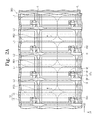
- FIG. 2A is an enlarged plan view of a portion of the display panel 300 of FIG. 1 , according to exemplary embodiments.
- FIG. 2B is a sectional view of the display panel 300 of FIG. 1 taken along sectional line I-F. It is noted that the elements illustrated in FIG. 2A primarily form the display substrate 100 of the display panel 300 . This limited plan view has been provided to reduce the complexity of the drawing and to provide a better mechanism to the understanding of exemplary embodiments described herein.
- the display panel 300 may include the display substrate 100 and the opposite substrate 200 .
- the display substrate 100 may be disposed closer to the backlight assembly 500 than the opposite substrate 200 .
- emitting lights ET 1 and ET 2 provided from the backlight assembly 500 may sequentially propagate through the display substrate 100 and the opposite substrate 200 to be emitted to the outside of the display panel 300 .
- the display substrate 100 may include a first substrate SUB 1 , which may be formed from any suitable material, such as, for instance, a transparent insulating material, e.g., glass, plastic, and/or the like. It is noted that the utilization of a transparent plastic substrate SUB 1 may provide for both transparency and flexibility characteristics.
- the first substrate SUB 1 may include a plurality of pixel regions (e.g., first to third pixel regions PA 1 , PA 2 , and PA 3 ) and a plurality of non-pixel regions (e.g., first and second non-pixel regions N-PA 1 and N-PA 2 ).
- a plurality of gate lines GL, a plurality of data lines DL, a plurality of switching elements (e.g., first to third thin-film transistors TR 1 , TR 2 , and TR 3 ), a plurality of pixel electrodes (e.g., first to third pixel electrodes PE 1 , PE 2 , and PE 3 ), a plurality of first optical elements L 1 , a plurality of second optical elements L 2 , and a first polarizing plate 10 may be provided on the first substrate SUB 1 .
- the plurality of gate lines GL may be provided on the first substrate SUB 1 to be electrically separated (or otherwise insulated) from the plurality of data lines DL.
- the plurality of gate lines GL and the plurality of data lines DL may be provided to cross each other, when viewed in a plan view.
- Each of the gate lines GL may be configured to deliver (or transmit) a gate signal, whereas each of the data lines DL may be configured to deliver a data signal.
- Each of the first to third thin-film transistors TR 1 , TR 2 , and TR 3 may be electrically connected to a corresponding one of the first to third pixel electrodes PE 1 , PE 2 , and PE 3 .
- the first to third thin-film transistors TR 1 , TR 2 , and TR 3 are substantially similar and the first to third pixel electrodes PE 1 , PE 2 , and PE 3 are substantially similar, and, therefore, to avoid obscuring exemplary embodiments described herein, the first thin-film transistor TR 1 and the first pixel electrode PE 1 will be described below as representative of each of corresponding components previously mentioned.
- the first thin-film transistor TR 1 may include a gate electrode GE, an active pattern AP, a source electrode SE, and a drain electrode DE.
- the gate electrode GE may be electrically connected to one of the plurality of gate lines GL to receive a gate signal.
- the active pattern AP may include any suitable semiconductor material, which may be provided on the gate electrode GE.
- a first insulating layer 21 may be provided between the active pattern AP and the gate electrode GE.
- the active pattern AP may include any suitable semiconductor material, such as, for example, amorphous or crystalline silicon. It is contemplated, however, that any other suitable material may be utilized in association with the active pattern AP.
- the active pattern AP may include at least one of various oxide semiconductor materials, such as, for instance, indium gallium zinc oxide (IGZO), zinc oxide (ZnO), tin dioxide (SnO 2 ), indium(III) oxide (In 2 O 3 ), zinc stannate (Zn 2 SnO 4 ), germanium oxide (Ge 2 O 3 ), hafnium(IV) oxide (HfO 2 ), etc., or compound semiconductor materials, such as, for instance, gallium arsenide (GaAs), gallium phosphide (GaP), indium phosphide (InP), etc.
- the semiconductor material may include any suitable semiconductor alloy with, for instance, an adjustable band gap, such as silicon germanium (Si 1-x Ge x
- the source electrode SE may be electrically connected to one of the data lines DL to receive a data signal.
- the source electrode SE may be provided on the active pattern AP.
- the drain electrode DE may be provided on the active pattern AP and may be spaced apart from the source electrode SE.
- a second insulating layer 22 may be provided to cover the plurality of thin-film transistors (e.g., thin-film transistors TR 1 , TR 2 , and TR 3 ), and a third insulating layer 23 may be provided on the second insulating layer 22 .
- a contact hole may be formed to penetrate the second insulating layer 22 and the third insulating layer 23 .
- the first pixel electrode PE 1 may be electrically connected to the drain electrode DE of the first thin-film transistor TR 1 through the contact hole.
- the gate signal is applied to the gate electrode GE and the first thin-film transistor TR 1 is “turned on,” the data signal may be transmitted to the first pixel electrode PE 1 through the source electrode SE, the active pattern AP, and the drain electrode DE.
- the plurality of first optical elements L 1 , an auxiliary layer 30 , and the plurality of second optical elements L 2 may be provided between the first polarizing plate 10 and the first substrate SUB 1 .
- the plurality of first optical elements L 1 may be positioned between the first substrate SUB 1 and the auxiliary layer 30 .
- the auxiliary layer 30 may be positioned between the plurality of first optical elements L 1 and the plurality of second optical elements L 2 .
- the plurality of second optical elements L 2 may be positioned between the first auxiliary layer 30 and the first polarizing plate 10 . Further, the plurality of first optical elements L 1 and the plurality of second optical elements L 2 may be alternatingly arranged with the auxiliary layer 30 disposed therebetween.
- a trough between adjacent first optical elements L 1 may be vertically (or substantially vertically) aligned with an apex of a second optical element L 2 .
- a trough between adjacent second optical elements L 2 may be vertically (or substantially vertically) aligned with an apex of a first optical element L 1 .
- a trough between adjacent second optical elements L 2 may be substantially aligned in association with a corresponding non-pixel area, such as the first non-pixel area N-PA 1 .
- each of the first optical elements L 1 may be shaped like a lens convexly protruding toward the first polarizing plate 10
- each of the second optical elements L 2 may be shaped like a lens convexly protruding toward the first substrate SUB 1
- the first and second optical elements L 1 and L 2 may be formed in any other suitable manner, such as, for example, as shown in FIG. 5 , where each of the first optical elements L 1 are shaped like a lens convexly protruding toward the first substrate SUB 1 , and each of the second optical elements L 2 are shaped like a lens convexly protruding toward the first polarizing plate 10 .
- the lens configurations of the first and second optical elements L 1 and L 2 may be formed in any suitable manner, such as, for example, in association with Fresnel formations, a saw-tooth formation, etc.
- the auxiliary layer 30 may include any suitable highly transparent material, such as, for instance, silicon oxide (SiO). As seen in the sectional view of FIG. 2B , the auxiliary layer 30 may have a curved bottom surface fitted to a profile of the first optical elements L 1 and a curved top surface fitted to a profile of the second optical elements L 2 .
- SiO silicon oxide
- the first optical elements L 1 are substantially similar, and, therefore, to avoid obscuring exemplary embodiments described herein, the first optical element L 1 disposed in association with the first pixel region PA 1 , the first non-pixel region N-PA 1 , and the third pixel region PA 3 will be described as a representative one of the plurality of first optical elements L 1 .
- the second optical elements L 2 are substantially similar, and, therefore, to avoid obscuring exemplary embodiments described herein, the second optical element L 2 disposed in association with the first non-pixel region N-PA 1 , the first pixel region PA 1 , and the second non-pixel region N-PA 2 will be described as a representative one of the plurality of second optical elements L 2 .
- the first and second optical elements L 1 and L 2 may have a thickness that decreases with increasing distance from a center (e.g., optical axis).
- a center e.g., optical axis
- the second thickness T 2 may be greater than the first thickness T 1 .
- an overall thickness of the second optical elements L 2 may be greater than the overall thickness of the first optical elements L 1 .
- the first optical element L 1 may have a first refracting surface S 1 , which may span a portion of the first pixel region PA 1 , the first non-pixel region N-PA 1 , and at least a portion of the third pixel region PA 3 , when viewed in a plan view. In this manner, the first optical element L 1 may overlap a border between the first pixel region PA 1 and the first non-pixel region N-PA 1 and a border between the first non-pixel region N-PA 1 and the third pixel region PA 3 .
- the second optical element L 2 may have a second refracting surface S 2 , which may span a portion of the first non-pixel region N-PA 1 , the first pixel region PA 1 , and a portion of the second non-pixel region N-PA 2 , when viewed in a plan view. In this manner, the second optical element L 2 may overlap a border between the first non-pixel region N-PA 1 and the first pixel region PA 1 and a border between the first pixel region PA 1 and the second non-pixel region N-PA 2 .
- the first refracting surface S 1 may have a curvature that is different from the curvature of the second refracting surface S 2 . It is contemplated, however, that exemplary embodiments are not limited thereto or thereby.
- the curvature of the first refracting surface S 1 may be substantially equivalent to the curvature of the second refracting surface S 2 .
- the light when light crosses an interface between a first transmission medium having a first refractive index and a second transmission medium having a second refractive index higher than the first refractive index, the light is refracted at the interface between the first and second transmission media. If the light passes through an interface shaped like a refracting surface of a concave lens, the light may be expanded. If the light passes through an interface shaped like a refracting surface of a convex lens, the light may be condensed.
- the first refracting surface S 1 may serve as a refracting surface of the concave lens.
- the first emitting light ET 1 may be expanded by the first refracting surface S 1 to be a first refracted light RT 1 propagating in a direction that is rotated clockwise by a first angle a 1 (which may be an acute angle) with respect to a normal direction of the first substrate SUB 1 .
- the light when light crosses an interface between a first transmission medium having a first refractive index and a second transmission medium having a second refractive index lower than the first refractive index, the light is refracted at the interface between the first and second transmission media. If the light passes through an interface shaped like a refracting surface of a concave lens, the light may be condensed. If the light passes through an interface shaped like a refracting surface of a convex lens, the light may be expanded.
- the second refracting surface S 2 may serve as a refracting surface of the concave lens.
- the first refracted light RT 1 may be expanded by the second refracting surface S 2 to be a second refracted light RT 2 propagating in a direction that is rotated counter-clockwise by a second angle a 2 with respect to a propagation direction of the first refracted light RT 1 .
- the first emitting light ET 1 propagating toward the first non-pixel region N-PA 1 may be refracted at the first refracting surface S 1 to be directed as the first refracted light RT 1 propagating toward the first pixel region PA 1 or toward an oblique direction with respect to the normal direction with respect to the first refracting surface S 1 .
- the first and second optical lenses L 1 and L 2 may be provided in such a way that the first angle a 1 and the second angle a 2 are substantially equivalent to each other. In this manner, the second refracted light RT 2 may propagate toward the first pixel region PA 1 along the normal direction with respect to the first refracting surface S 1 .
- the first emitting light ET 1 may propagate toward the first non-pixel region N-PA 1 , and, as such, it may not be used to display an image, e.g., it may be blocked by, for instance, a light shielding layer BM, which will be described in more detail in the proceeding paragraphs.
- the first and second optical elements L 1 and L 2 may be used to change the propagation direction of the first emitting light ET 1 toward the first pixel region PA 1 .
- the first emitting light ET 1 may be used to display an image, and, as such, it may be possible to increase the light efficiency of the light emitted from the backlight assembly 500 . Further, since the second refracted light RT 2 propagates parallel to the normal direction and may be emitted to the outside through the first pixel region PA 1 , the first pixel region PA 1 may have an improved frontal brightness.
- the second emitting light ET 2 may pass through an interface between a pair of the first optical elements L 1 adjacent to each other (e.g., pass through a trough) and be incident to a central region (e.g., optical axis) of the second optical element L 2 .
- the propagation direction of the second emitting light ET 2 may not be changed.
- the propagation direction of the second emitting light ET 2 may remain parallel to the normal direction with respect to the first reacting surface S 1 .
- the first polarizing plate 10 may be provided to face the first to third thin-film transistors TR 1 , TR 2 , and TR 3 and the first to third pixel electrodes PE 1 , PE 2 , and PE 3 .
- an interlayer insulating layer 20 may be disposed between the first polarizing plate 10 and the first insulating layer 20 .
- the first polarizing plate 10 may be provided between the first substrate SUB 1 and the liquid crystal layer LC, and, thereby, configured to polarize light propagating from the backlight assembly 500 towards the liquid crystal layer LC.
- the first polarizing plate 10 may include a plurality of grid polarizing layers 15 containing any suitable reflective material, e.g., any suitable reflective metal material.
- the first polarizing plate 10 may be configured to transmit a fraction of incident light depending on its polarization.
- Each of the grid polarizing layers 15 may longitudinally extend in (or substantially in) a first direction D 1 , e.g., a vertical direction.
- the grid polarizing layers 15 may be arranged so as to be spaced apart from each other in (or substantially) in a second direction D 2 , e.g., horizontal direction. If a pitch of the grid polarizing layers 15 is smaller than a wavelength of incident light incident, the grid polarizing layers 15 may serve as a wire grid polarizer or diffraction grating polarizer.
- the opposite substrate 200 may include a second substrate SUB 2 , a common electrode CE, a light-shielding layer BM, a color filter CF, and a second polarizing plate 210 .
- the second substrate SUB 2 may be formed from any suitable transparent substrate material, e.g., glass, plastic, etc., which may be similar to the transparent substrate material of the first substrate SUB 1 .
- the common electrode CE may be provided on the second substrate SUB 2 , and the common electrode CE may be provided to face the first to third pixel electrodes PE 1 , PE 2 , and PE 3 .
- the liquid crystal layer LC may be disposed between the common electrode CE and the first to third pixel electrodes PE 1 , PE 2 , and PE 3 .
- the common electrode CE may be used in conjunction with one or more of the first to third pixel electrodes PE 1 , PE 2 , and PE 3 to produce an electric field, which may be utilized to control an orientation of liquid crystal molecules (not shown) of the liquid crystal layer LC.
- the light-shielding layer BM may be provided on the second substrate SUB 2 to correspond to each of the non-pixel regions (e.g., the first and second non-pixel regions N-PA 1 and N-PA 2 ).
- the color filter CF may be provided on the second substrate SUB 2 to correspond to each of the pixel regions (e.g., the first to third pixel regions PA 1 , PA 2 , and PA 3 ). It is noted that the use of the color filters CF may enable the display device to display a color image.
- the second polarizing plate 210 may be disposed on a surface of the second substrate SUB 2 and, thereby, configured to polarize incident light propagating from the liquid crystal layer LC towards and through the second polarizing plate 210 . It is contemplated, however, that any suitable second polarizing plate 210 may be utilized.
- the second polarizing plate 210 may be provided in the form of a wire grid polarizer (or diffraction grating polarizer), which may be similar to the first polarizing plate 10 .
- FIGS. 3-19 are respective sectional views of display devices including display panels, according to exemplary embodiments. It is noted that the display devices including the display panels of FIGS. 3-17 are substantially similar to the display device including the display panel of FIGS. 1, 2A, and 2B . As such, to avoid obscuring exemplary embodiments described herein, primarily differences between these display devices will be described in the proceeding paragraphs.
- a display panel 301 may include a display substrate 101 and an opposite substrate 200 .
- the display substrate 101 may include a plurality of first optical elements L 1 _ 1 , an auxiliary layer 31 , and a plurality of second optical elements L 2 _ 1 .
- each of the plurality of first optical elements L 1 _ 1 may be provided to face a corresponding one of the plurality of second optical elements L 2 _ 1 with the auxiliary layer 31 disposed therebetween.
- an apex of a first optical element L 1 _ 1 may be vertically (or substantially vertically) aligned with a corresponding apex of a second optical element L 2 _ 1 .
- a trough between adjacent first optical elements L 1 _ 1 may be vertically (or substantially vertically) aligned with a corresponding trough between adjacent second optical elements L 2 _ 1 . Further, it is noted that an overall thickness of the second optical elements L 2 _ 1 may be greater than the overall thickness of the first optical elements L 1 _ 1 .
- each of the first optical elements L 1 _ 1 may have a refractive index greater than the refractive index of the auxiliary layer 31 .
- Each of the second optical elements L 2 _ may have a refractive index smaller than the refractive index of the auxiliary layer 31 .
- the first refracting surface S 1 may serve as a refracting surface of a convex lens
- the second refracting surface S 2 may serve as a refracting surface of a concave lens.
- an emitting light ET may be refracted at the first refracting surface S 1 and the second refracting surface S 2 , so as to be redirected, and, thereby, propagated toward the first pixel region PA 1 in a direction parallel to the normal direction with respect to the first substrate SUB 1 .
- a display panel 302 may include a display substrate 102 and an opposite substrate 200 .
- the display substrate 102 may include a plurality of first optical elements L 1 _ 2 , an auxiliary layer 32 , and a plurality of second optical elements L 2 _ 2 .
- the plurality of first optical elements L 1 _ 2 and the plurality of second optical elements L 2 _ 2 may be alternatingly arranged with the auxiliary layer 32 disposed therebetween. For instance, a trough between adjacent first optical elements L 1 may be vertically (or substantially vertically) aligned with an apex of a second optical element L 2 .
- a trough between adjacent second optical elements L 2 may be vertically (or substantially vertically) aligned with an apex of a first optical element L 1 .
- a trough between adjacent first optical elements L 1 _ 2 shown in FIG. 4 may be substantially aligned in association with a corresponding non-pixel area, such as the first non-pixel area N-PA 1 .
- an overall thickness of the second optical elements L 2 _ 2 may be greater than the overall thickness of the first optical elements L 1 _ 2 .
- each of the first optical elements L 1 _ 2 may have a refractive index greater than the refractive index of the auxiliary layer 32
- each of the second optical elements L 2 _ 2 may have a refractive index greater than refractive index of the auxiliary layer 32 .
- the first refracting surface S 1 may serve as a refracting surface of a concave lens
- the second refracting surface S 2 may serve as a refracting surface of a convex lens.
- an emitting light ET may be refracted at the first refracting surface S 1 and the second refracting surface S 2 , so as to be redirected, and, thereby, propagated toward the first pixel region PA 1 in a direction parallel to the normal direction with respect to the first substrate SUB 1 .
- a display panel 303 may include a display substrate 103 and the opposite substrate 200 .
- the display substrate 103 may include a plurality of first optical elements L 1 _ 3 , a first auxiliary layer 33 , a plurality of second optical elements L 2 _ 3 , and a second auxiliary layer 53 .
- the first auxiliary layer 33 may be disposed between the first substrate SUB 1 and the plurality of first optical elements L 1 _ 3
- the second auxiliary layer 53 may be disposed between the first polarizing plate 10 and the plurality of second optical elements L 2 _ 3 .
- the plurality of second optical elements L 2 _ 3 may be disposed directly on the plurality of first optical elements L 1 _ 3 .
- first optical elements L 1 _ 3 and the plurality of second optical elements L 2 _ 3 maybe alternatingly arranged with respect to each other.
- an apex of a first optical element L 1 _ 3 may be vertically (or substantially vertically) aligned with a corresponding apex of a second optical element L 2 _ 3 .
- a trough between adjacent first optical elements L 1 _ 3 may be disposed in association with a non-pixel region, such as the first non-pixel region N-PA 1 .
- an overall thickness of the first optical elements L 1 _ 3 may be greater than the overall thickness of the second optical elements L 2 _ 3 .
- Each of the first optical elements L 1 _ 3 may have a first refractive index
- the first auxiliary layer 33 may have a second refractive index
- the plurality of second optical elements L 2 _ 3 may have a third refractive index
- the second auxiliary layer 53 may have a fourth refractive index.
- the first refractive index may be greater than the second refractive index and be smaller than the third refractive index.
- the third refractive index may be greater than the fourth refractive index.
- the first refracting surface S 1 may serve as a refracting surface of a convex lens
- the second refracting surface S 2 may serve as a refracting surface of a concave lens.
- an emitting light ET may be refracted at the first refracting surface S 1 to be redirected as a first refracted light RT 1
- the first refracted light RT 1 may be refracted at interface BS between the first and second optical elements L 1 _ 3 and L 2 _ 3 to be redirected as a second refracted light RT 2 .
- the second refracted light RT 2 may be refracted at the second refracting surface S 2 to be redirected as a third refracted light RT 3 propagating toward the first pixel region PA 1 in a direction parallel to the normal direction with respect to the first substrate SUB 1 .
- a display panel 304 may include a display substrate 104 and the opposite substrate 200 .
- the display substrate 104 may include a plurality of first optical elements L 1 _ 4 , an auxiliary layer 34 , and a plurality of second optical elements L 2 _ 4 .
- the auxiliary layer 34 may be provided between the first substrate SUB 1 and the plurality of first optical elements L 1 _ 4 .
- the display substrate 104 of FIG. 6 includes the second optical elements L 2 _ 4 disposed directly on the first optical elements L 1 _ 4 , such that no auxiliary layer is disposed between the second optical elements L 2 _ 4 and the first optical elements L 1 _ 4 .
- troughs between adjacent second optical elements L 2 _ 4 may be disposed in association with corresponding non-pixel regions, such as the first non-pixel region N-PA 1 .
- apexes between adjacent first optical elements L 1 _ 4 may also be disposed in association with corresponding non-pixel regions, such as the first non-pixel region N-PA 1 .
- troughs between adjacent first optical elements L 1 _ 4 may be vertically (or substantially vertically) aligned with respective apexes of the second optical elements L 2 _ 4 .
- the auxiliary layer 34 may have a refractive index greater than the refractive index of each of the first optical elements L 1 _ 4 , and each of the first optical elements L 1 _ 4 may have a refractive index greater than the refractive index of each of the second optical elements L 2 _ 4 .
- the first refracting surface S 1 may serve as a refracting surface of a convex lens
- the second refracting surface S 2 may serve as a refracting surface of a convex lens.
- an emitting light ET may be refracted at the first refracting surface S 1 and the second refracting surface S 2 , so as to be redirected toward the first pixel region PA 1 and in a direction parallel to the normal direction with respect to the first substrate SUB 1 .
- a display panel 305 may include a display substrate 105 and the opposite substrate 200 .
- the display substrate 105 may include a plurality of first optical elements L 1 _ 5 , an auxiliary layer 35 , and a plurality of second optical elements L 2 _ 5 .
- the auxiliary layer 35 may be provided between the first substrate SUB 1 and the plurality of first optical elements L 1 _ 5 .
- the display substrate 105 of FIG. 7 includes the second optical elements L 2 _ 5 disposed directly on the first optical elements L 1 _ 5 , such that no auxiliary layer is disposed between the second optical elements L 2 _ 5 and the first optical elements L 1 _ 5 .
- Troughs between adjacent first optical elements L 1 _ 5 may be disposed in association with corresponding non-pixel regions, such as the first non-pixel region N-PA 1 .
- apexes between adjacent second optical elements L 2 _ 5 may also be disposed in association with corresponding non-pixel regions, such as the first non-pixel region N-PA 1 .
- troughs between adjacent first optical elements L 1 _ 5 may be vertically (or substantially vertically) aligned with respective apexes of the second optical elements L 2 _ 5 .
- each of the first optical elements L 1 _ 5 may have a refractive index greater than the refractive index of the auxiliary layer 35 , and each of the first optical elements L 1 _ 5 may have a refractive index that is smaller than the refractive index of each of the second optical elements L 2 _ 5 .
- the first refracting surface S 1 may serve as a refracting surface of a convex lens
- the second refracting surface S 2 may serve as a refracting surface of a convex lens.
- an emitting light ET may be refracted at the first refracting surface S 1 and the second refracting surface S 2 , so as to be redirected and, thereby, propagated toward the first pixel region PA 1 in a direction parallel to the normal direction with respect to the first substrate SUB 1 .
- a display panel 306 may include a display substrate 106 and the opposite substrate 200 .
- the display substrate 106 may include a plurality of first optical elements L 1 _ 6 , an auxiliary layer 36 , and a plurality of second optical elements L 2 _ 6 .
- the auxiliary layer 36 may be provided between the plurality of first optical elements L 1 _ 6 and the plurality of second optical elements L 2 _ 6 .
- Each of the first optical elements L 1 _ 6 may be provided to face a corresponding one of the second optical elements L 2 _ 6 with the auxiliary layer 36 disposed therebetween.
- respective apexes of the first and second optical elements L 1 _ 6 and L 2 _ 6 may be vertically (or substantially vertically) aligned with one another. Moreover, the respective apexes of the first and second optical elements L 1 _ 6 and L 2 _ 6 may be aligned in association with a corresponding non-pixel region, such as the first non-pixel region N-PA 1 . Further, it is noted that an overall thickness of the second optical elements L 2 _ 6 may be greater than the overall thickness of the first optical elements L 1 _ 6 .
- each of the first optical elements L 1 _ 6 may have a refractive index smaller than the refractive index of the auxiliary layer 36
- the auxiliary layer 36 may have a refractive index smaller than the refractive index of each of the second optical elements L 1 _ 6 .
- the first refracting surface S 1 may serve as a refracting surface of a concave lens
- the second refracting surface S 2 may serve as a refracting surface of a convex lens.
- an emitting light ET may be refracted at the first refracting surface S 1 and the second refracting surface S 2 , so as to be redirected and, thereby, propagated towards the first pixel region PA 1 in a direction parallel to the normal direction with respect to the first substrate SUB 1 .
- a display panel 307 may include a display substrate 107 and the opposite substrate 200 .
- the display substrate 107 may include a plurality of first optical elements L 1 _ 7 , a first auxiliary layer 37 , a plurality of second optical elements L 2 _ 7 , and a second auxiliary layer 57 .
- the first auxiliary layer 37 may be provided between the first substrate SUB 1 and the first optical elements L 1 _ 7
- the second auxiliary layer 57 may be provided between the first polarizing plate 10 and the second optical elements L 2 _ 7 .
- each of the first optical elements L 1 _ 7 may have a refractive index greater than the refractive index of the first auxiliary layer 37 , and each of the first optical elements L 1 _ 7 may have a refractive index smaller than the refractive index of each of the second optical elements L 2 _ 7 .
- the second auxiliary layer 57 may have a refractive index greater than the refractive index of each of the second optical elements L 2 _ 7 .
- respective troughs of the first and second optical elements L 1 _ 7 and L 2 _ 7 may be vertically (or substantially vertically) aligned with one another, as well as respectively aligned in association with a corresponding non-pixel region, such as the first non-pixel region N-PA 1 . Further, it is noted that an overall thickness of the first optical elements L 1 _ 7 may be greater than the overall thickness of the second optical elements L 2 _ 7 .
- the first refracting surface S 1 may serve as a refracting surface of a convex lens
- the second refracting surface S 2 may serve as a refracting surface of a concave lens.
- the emitting light ET may be refracted at the first refracting surface S 1 to be redirected as a first refracted light RT 1
- the first refracted light RT 1 may be refracted at an interface BS between the first and second optical elements L 1 _ 7 and L 2 _ 7 to be redirected as a second refracted light RT 2 .
- the second refracted light RT 2 may be refracted at the second refracting surface S 2 to be redirected as a third refracted light RT 3 propagating towards the first pixel region PA 1 in a direction parallel to the normal direction with respect to the first substrate SUB 1 .
- a display panel 308 may include a display substrate 108 and the opposite substrate 200 .
- the display substrate 108 may include a plurality of first optical elements L 1 _ 8 , a first auxiliary layer 38 , a plurality of second optical elements L 2 _ 8 , and a second auxiliary layer 58 .
- the first auxiliary layer 38 may be provided between the first substrate SUB 1 and the first optical elements L 1 _ 8
- the second auxiliary layer 58 may be provided between the first polarizing plate 10 and the second optical elements L 2 _ 8 .
- respective apexes of the first and second optical elements L 1 _ 8 and L 2 _ 8 may be vertically (or substantially vertically) aligned with one another, as well as respectively aligned in association with a corresponding non-pixel region, such as the first non-pixel region N-PA 1 . Further, it is noted that an overall thickness of the first optical elements L 1 _ 8 may be greater than the overall thickness of the second optical elements L 2 _ 8 .
- each of the first optical elements L 1 _ 8 may have a refractive index smaller than the refractive index of the first auxiliary layer 38 , and each of the first optical elements L 1 _ 8 may have a refractive index smaller than the refractive index of each of the second optical elements L 2 _ 8 .
- the second auxiliary layer 58 may have a refractive index smaller than the refractive index of each of the second optical elements L 2 _ 8 .
- the first refracting surface S 1 may serve as a refracting surface of a convex lens
- the second refracting surface S 2 may serve as a refracting surface of a concave lens.
- an emitting light ET may be refracted at the first refracting surface S 1 , the interface BS, and the second refracting surface S 2 , so as to be redirected and, thereby, propagated towards the first pixel region PA 1 in a direction parallel to the normal direction with respect to the first substrate SUB 1 .
- a display panel 309 may include a display substrate 109 and the opposite substrate 200 .
- the display substrate 109 may include a plurality of first optical elements L 1 _ 9 , a first auxiliary layer 39 , a plurality of second optical elements L 2 _ 9 , and a second auxiliary layer 59 .
- the first auxiliary layer 39 may be provided between the first optical elements L 1 _ 9 and the second optical elements L 2 _ 9
- the second auxiliary layer 59 may be provided between the second optical elements L 2 _ 9 and the first polarizing plate 10 .
- troughs between adjacent second optical elements L 2 _ 9 may be disposed in association with corresponding non-pixel regions, such as the first non-pixel region N-PA 1 .
- apexes between adjacent first optical elements L 1 _ 9 may also be disposed in association with corresponding non-pixel regions, such as the first non-pixel region N-PA 1 .
- troughs between adjacent first optical elements L 1 _ 9 may be vertically (or substantially vertically) aligned with respective apexes of the second optical elements L 2 _ 9 .
- each of the first optical elements L 1 _ 9 may have a refractive index smaller than the refractive index of the first auxiliary layer 39
- the first auxiliary layer 39 may have a refractive index smaller than the refractive index of each of the second optical elements L 2 _ 9
- the second auxiliary layer 59 may have a refractive index greater than the refractive index of each of the second optical elements L 2 _ 9 .
- the first refracting surface S 1 may serve as a refracting surface of a concave lens
- the second refracting surface S 2 may also serve as a refracting surface of a concave lens.
- an emitting light ET may be refracted at the first refracting surface S 1 , the interface BS, and the second refracting surface S 2 , so as to be redirected and, thereby, propagated towards the first pixel region PA 1 in a direction parallel to the normal direction with respect to the first substrate SUB 1 .
- a display panel 310 may include a display substrate 110 and the opposite substrate 200 .
- the display substrate 110 may include a plurality of first optical elements L 1 _ 10 , a first auxiliary layer 40 , a plurality of second optical elements L 2 _ 10 , and a second auxiliary layer 60 .
- the first auxiliary layer 40 may be provided between the first and second optical elements L 1 _ 10 and L 2 _ 10
- the second auxiliary layer 60 may be provided between the second optical elements L 2 _ 10 and the first polarizing plate 10 .
- troughs between adjacent first optical elements L 1 _ 10 may be disposed in association with corresponding non-pixel regions, such as the first non-pixel region N-PA 1 .
- apexes between adjacent second optical elements L 1 _ 10 may also be disposed in association with corresponding non-pixel regions, such as the first non-pixel region N-PA 1 .
- troughs between adjacent first optical elements L 1 _ 10 may be vertically (or substantially vertically) aligned with respective apexes of the second optical elements L 2 _ 10 .
- each of the first optical elements L 1 _ 10 may have a refractive index greater than the refractive index of the first auxiliary layer 40
- the first auxiliary layer 40 may have a refractive index smaller than the refractive index of each of the second optical elements L 2 _ 10
- the second auxiliary layer 60 may have a refractive index smaller than the refractive index of each of the second optical elements L 2 _ 10 .
- the first refracting surface S 1 may serve as a refracting surface of a concave lens
- the second refracting surface S 2 may also serve as a refracting surface of a concave lens.
- an emitting light ET may be refracted at the first refracting surface S 1 , the interface BS, and the second refracting surface S 2 , so as to be redirected and, thereby, propagated towards the first pixel region PA 1 in a direction parallel to the normal direction with respect to the first substrate SUB 1 .
- a display panel 311 may include a display substrate 111 and the opposite substrate 200 .
- the display substrate 111 may include a plurality of first optical elements L 1 _ 11 , a first auxiliary layer 41 , a plurality of second optical elements L 2 _ 11 , and a second auxiliary layer 61 .
- the first auxiliary layer 41 may be provided between the first optical elements L 1 _ 11 and the second optical elements L 2 _ 11
- the second auxiliary layer 61 may be provided between the second optical elements L 2 _ 11 and the first polarizing plate 10 .
- respective troughs between the first and second optical elements L 1 _ 11 and L 2 _ 11 may be vertically (or substantially vertically) aligned with one another, as well as respectively aligned in association with a corresponding non-pixel region, such as the first non-pixel region N-PA 1 .
- each of the first optical elements L 1 _ 11 may have a refractive index greater than the refractive index of the first auxiliary layer 41
- the first auxiliary layer 41 may have a refractive index smaller than the refractive index of each of the second optical elements L 2 _ 11
- the second auxiliary layer 59 may have a refractive index greater than the refractive index of each of the second optical elements L 2 _ 9 .
- the first refracting surface S 1 may serve as a refracting surface of a concave lens
- the second refracting surface S 2 may also serve as a refracting surface of a concave lens.
- an emitting light ET may be refracted at the first refracting surface S 1 , the interface BS, and the second refracting surface S 2 , so as to be redirected and, thereby, propagated towards the first pixel region PA 1 in a direction parallel to the normal direction with respect to the first substrate SUB 1 .
- a display panel 312 may include a display substrate 112 and the opposite substrate 200 .
- the display substrate 112 may include a plurality of first optical elements L 1 _ 12 , a first auxiliary layer 42 , a plurality of second optical elements L 2 _ 12 , and a second auxiliary layer 62 .
- the first auxiliary layer 42 may be provided between the first optical elements L 1 _ 12 and the second optical elements L 2 _ 12
- the second auxiliary layer 62 may be provided between the second optical elements L 2 _ 12 and the first polarizing plate 10 .
- respective apexes of the first and second optical elements L 1 _ 12 and L 2 _ 12 may be vertically (or substantially vertically) aligned with one another, as well as respectively aligned in association with a corresponding non-pixel region, such as the first non-pixel region N-PA 1 .
- each of the first optical elements L 1 _ 12 may have a refractive index smaller than the refractive index of the first auxiliary layer 42
- the first auxiliary layer 42 may have a refractive index smaller than the refractive index of each of the second optical elements L 2 _ 12
- the second auxiliary layer 62 may have a refractive index smaller than the refractive index of each of the second optical elements L 2 _ 12 .
- the first refracting surface S 1 may serve as a refracting surface of a concave lens
- a second refracting surface S 2 may also serve as a refracting surface of a concave lens.
- an emitting light ET may be refracted at the first refracting surface S 1 , the interface BS, and the second refracting surface S 2 , so as to be redirected and, thereby, propagated towards the first pixel region PA 1 in a direction parallel to the normal direction with respect to the first substrate SUB 1 .
- a display panel 313 may include a display substrate 113 and the opposite substrate 200 .
- the display substrate 113 may include a plurality of first optical elements L 1 _ 13 , an auxiliary layer 43 , and a plurality of second optical elements L 2 _ 13 .
- the auxiliary layer 43 may be provided between the first substrate SUB 1 and the first optical elements L 1 _ 13 .
- the display substrate 113 of FIG. 15 includes the second optical elements L 2 _ 13 disposed directly on the first optical elements L 1 _ 13 , such that no auxiliary layer is disposed between the second optical elements L 2 _ 13 and the first optical elements L 1 _ 13 .
- troughs between respective adjacent first optical elements L 1 _ 13 and respective adjacent second optical elements L 2 _ 13 may be disposed in association with corresponding non-pixel regions, such as the first non-pixel region N-PA 1 .
- the respective troughs between adjacent first optical elements L 1 _ 13 and between adjacent second optical elements L 2 _ 13 may be vertically (or substantially vertically) aligned with one another, and the respective apexes between adjacent first optical elements L 1 _ 13 and between adjacent second optical elements L 2 _ 13 may be vertically (or substantially vertically) aligned with one another.
- an overall thickness of the second optical elements L 2 _ 13 may be greater than the overall thickness of the first optical elements L 1 _ 13 .
- the auxiliary layer 43 may have a refractive index smaller than the refractive index of each of the first optical elements L 1 _ 13 , and each of the first optical elements L 1 _ 13 may have a refractive index greater than the refractive index of each of the second optical elements L 2 _ 13 .
- the first refracting surface S 1 may serve as a refracting surface of a convex lens
- the second refracting surface S 2 may also serve as a refracting surface of a convex lens.
- an emitting light ET may be refracted at the first refracting surface S 1 and the second refracting surface S 2 , so as to be redirected and, thereby, propagated towards the first pixel region PA 1 in a direction parallel to the normal direction with respect to the first substrate SUB 1 .
- a display panel 314 may include a display substrate 114 and the opposite substrate 200 .
- the display substrate 114 may include a plurality of first optical elements L 1 _ 14 , an auxiliary layer 44 , and a plurality of second optical elements L 2 _ 14 .
- the auxiliary layer 44 may be provided between the first substrate SUB 1 and the first optical elements L 1 _ 14 .
- the display substrate 114 of FIG. 16 includes the second optical elements L 2 _ 14 disposed directly on the first optical elements L 1 _ 14 , such that no auxiliary layer is disposed between the second optical elements L 2 _ 14 and the first optical elements L 1 _ 14 .
- apexes between respective adjacent first optical elements L 1 _ 14 and respective adjacent second optical elements L 2 _ 14 may be disposed in association with corresponding non-pixel regions, such as the first non-pixel region N-PA 1 .
- the respective troughs between adjacent first optical elements L 1 _ 14 and between adjacent second optical elements L 2 _ 14 may be vertically (or substantially vertically) aligned with one another, and the respective apexes between adjacent first optical elements L 1 _ 14 and between adjacent second optical elements L 2 _ 14 may be vertically (or substantially vertically) aligned with one another.
- an overall thickness of the second optical elements L 2 _ 14 may be greater than the overall thickness of the first optical elements L 1 _ 14 .
- the auxiliary layer 44 may have a refractive index greater than the refractive index of each of the first optical elements L 1 _ 14 , and each of the first optical elements L 1 _ 14 may have a refractive index smaller than the refractive index of each of the second optical elements L 2 _ 14 .
- the first refracting surface S 1 may serve as a refracting surface of a convex lens
- the second refracting surface S 2 may also serve as a refracting surface of a convex lens.
- an emitting light ET may be refracted at the first refracting surface S 1 and the second refracting surface S 2 , so as to be redirected and, thereby, propagated towards the first pixel region PA 1 in a direction parallel to the normal direction with respect to the first substrate SUB 1 .
- a display panel 315 may include a display substrate 115 and the opposite substrate 200 .
- the display substrate 115 may include a plurality of first optical elements L 1 _ 15 , an auxiliary layer 45 , and a plurality of second optical elements L 2 _ 15 .
- the auxiliary layer 45 may be provided between the first optical elements L 1 _ 15 and the second optical elements L 2 _ 15 .
- each of the first and second optical elements L 1 and L 2 may be shaped like a lens, and, as such, each of the first and second refracting surfaces S 1 and S 2 may have a curved (or otherwise arcuate) surface.
- the first refracting surface S 1 of the first optical elements L 1 _ 15 may be a flat, angled surface
- the second refracting surface S 2 of the second optical elements L 2 _ 15 may be a flat, angled surface. In this manner, the first and second refracting surfaces S 1 and S 2 may resemble saw tooth surfaces.
- troughs between adjacent second optical elements L 2 _ 15 may be disposed in association with corresponding non-pixel regions, such as the first non-pixel region N-PA 1 .
- apexes between adjacent first optical elements L 1 _ 15 may also be disposed in association with corresponding non-pixel regions, such as the first non-pixel region N-PA 1 .
- troughs between adjacent first optical elements L 1 _ 15 may be vertically (or substantially vertically) aligned with respective apexes of the second optical elements L 2 _ 15 .
- an overall thickness of the second optical elements L 2 _ 15 may be greater than the overall thickness of the first optical elements L 1 _ 15 .
- a display panel 316 may include a display substrate 116 and the opposite substrate 200 .
- the display substrate 116 may include a plurality of first optical elements L 1 _ 15 , a first auxiliary layer 46 , a plurality of second optical elements L 2 _ 16 , and a second auxiliary layer 63 .
- the first auxiliary layer 46 may be disposed between the first substrate SUB 1 and the plurality of first optical elements L 1 _ 16
- the second auxiliary layer 63 may be disposed between the first polarizing plate 10 and the plurality of second optical elements L 2 _ 16 .
- Each of the first optical elements L 1 _ 16 may have a first refractive index
- the first auxiliary layer 46 may have a second refractive index
- the plurality of second optical elements L 2 _ 16 may have a third refractive index
- the second auxiliary layer 63 may have a fourth refractive index.
- the first refractive index may be greater than the second refractive index and may be smaller than the third refractive index.
- the third refractive index may be greater than the fourth refractive index.
- the first refracting surface S 1 may serve as a refracting surface of a convex lens
- the second refracting surface S 2 may serve as a refracting surface of a concave lens.
- an emitting light ET may be refracted at the first refracting surface S 1 to be redirected as a first refracted light RT 1
- the first refracted light RT 1 may be refracted at interface BS between the first and second optical elements L 1 _ 16 and L 2 _ 16 to be redirected as a second refracted light RT 2 .
- the second refracted light RT 2 may be refracted at the second refracting surface S 2 to be redirected as a third refracted light RT 3 propagating toward the first pixel region PA 1 in a direction parallel to the normal direction with respect to the first substrate SUB 1 .
- the plurality of first optical elements L 1 _ 3 and the plurality of second optical elements L 2 _ 3 were alternatingly arranged with respect to each other.
- a trough between adjacent second optical elements L 2 _ 16 may be disposed in association with a non-pixel region, such as the first non-pixel region N-PA 1 .
- FIG. 18 a trough between adjacent second optical elements L 2 _ 16 may be disposed in association with a non-pixel region, such as the first non-pixel region N-PA 1 .
- the plurality of first optical elements L 1 _ 16 and the plurality of second optical elements L 2 _ 16 maybe alternatingly arranged with respect to each other, such that an trough of a first optical element L 1 _ 16 may be vertically (or substantially vertically) aligned with a corresponding apex of a second optical element L 2 _ 16 .
- a display panel 317 may include a display substrate 117 and the opposite substrate 200 .
- the display substrate 117 may include a plurality of first optical elements L 1 _ 17 , an auxiliary layer 47 , and a plurality of second optical elements L 2 _ 17 .
- the auxiliary layer 47 may be provided between the first optical elements L 1 _ 17 and the second optical elements L 2 _ 17 .
- each of the first and second optical elements L 1 _ 2 and L 2 _ 2 may be shaped like a lens, and, as such, each of the first and second refracting surfaces S 1 and S 2 may have a curved (or otherwise arcuate) surface.
- the first refracting surface S 1 of the first optical elements L 1 _ 17 may be a flat, angled surface
- the second refracting surface S 2 of the second optical elements L 2 _ 17 may be a flat, angled surface. In this manner, the first and second refracting surfaces S 1 and S 2 may resemble saw tooth surfaces.
- apexes between adjacent second optical elements L 2 _ 17 may be disposed in association with corresponding non-pixel regions, such as the first non-pixel region N-PA 1 .
- troughs between adjacent first optical elements L 1 _ 17 may also be disposed in association with corresponding non-pixel regions, such as the first non-pixel region N-PA 1 .
- troughs between adjacent first optical elements L 1 _ 17 may be vertically (or substantially vertically) aligned with respective apexes of the second optical elements L 2 _ 17 .
- an overall thickness of the second optical elements L 2 _ 17 may be greater than the overall thickness of the first optical elements L 1 _ 17 .
- each of the first and second optical elements of FIGS. 3-16 and 18 may be replaced with corresponding first and second optical elements including flat, angled surfaces as opposed to the respectively illustrated arcuate surfaces.
- the respective surfaces may additionally or alternatively be configured as a Fresnel lens or any other suitable shape to achieve one or more of the light redirecting effects described herein.
- At least the first and second optical elements may be utilized to direct self-emitted light from a non-pixel region through a pixel region to increase light efficiency and/or frontal brightness.
- at least the first and second optical elements may be disposed between a substrate including a light emitting component of the associated display device and the light shielding layer BM. It is noted that the backlight assembly 500 may be omitted in such embodiments.
- a fraction of emitting light propagating toward a non-pixel region may be redirected by first and second optical elements, and, thereby, be emitted through a pixel region of a corresponding display panel.
- the redirected fraction of the emitting light may be used to facilitate the display of an image via the display panel. This may increase the light efficiency associated with the backlight assembly.
- the light redirected by the first and second optical elements may be emitted in a direction normal to a substrate surface, a frontal brightness of the display panel may be increased.
Applications Claiming Priority (2)
| Application Number | Priority Date | Filing Date | Title |
|---|---|---|---|
| KR10-2013-0043119 | 2013-04-18 | ||
| KR1020130043119A KR102060793B1 (ko) | 2013-04-18 | 2013-04-18 | 표시 장치 |
Publications (2)
| Publication Number | Publication Date |
|---|---|
| US20140313455A1 US20140313455A1 (en) | 2014-10-23 |
| US9423646B2 true US9423646B2 (en) | 2016-08-23 |
Family
ID=51728751
Family Applications (1)
| Application Number | Title | Priority Date | Filing Date |
|---|---|---|---|
| US14/040,236 Active 2034-07-12 US9423646B2 (en) | 2013-04-18 | 2013-09-27 | Display device |
Country Status (2)
| Country | Link |
|---|---|
| US (1) | US9423646B2 (ko) |
| KR (1) | KR102060793B1 (ko) |
Cited By (3)
| Publication number | Priority date | Publication date | Assignee | Title |
|---|---|---|---|---|
| US20180081238A1 (en) * | 2016-09-21 | 2018-03-22 | Boe Technology Group Co., Ltd. | Display panel, display apparatus and manufacturing method of display panel |
| US20190163023A1 (en) * | 2017-11-27 | 2019-05-30 | Samsung Display Co. Ltd. | Color conversion substrate and liquid-crystal display device including the same |
| WO2021241127A1 (ja) * | 2020-05-25 | 2021-12-02 | ソニーセミコンダクタソリューションズ株式会社 | 電気光学基板、液晶表示装置および電子機器 |
Families Citing this family (5)
| Publication number | Priority date | Publication date | Assignee | Title |
|---|---|---|---|---|
| CN105700212A (zh) * | 2016-04-11 | 2016-06-22 | 京东方科技集团股份有限公司 | 一种显示装置 |
| JP6531801B2 (ja) * | 2017-08-29 | 2019-06-19 | セイコーエプソン株式会社 | 電気光学装置用基板、電気光学装置、および電子機器 |
| CN109936890B (zh) * | 2017-12-18 | 2022-03-15 | 群创光电股份有限公司 | 电子装置 |
| KR102391028B1 (ko) * | 2019-01-25 | 2022-04-25 | 삼성에스디아이 주식회사 | 편광판 및 이를 포함하는 광학표시장치 |
| JP6806184B2 (ja) * | 2019-05-15 | 2021-01-06 | セイコーエプソン株式会社 | 電気光学装置用基板、電気光学装置、および電子機器 |
Citations (28)
| Publication number | Priority date | Publication date | Assignee | Title |
|---|---|---|---|---|
| US5808712A (en) * | 1995-09-28 | 1998-09-15 | Sharp Kabushiki Kaisha | Transmission liquid crystal display device with a liquid crystal panel having high luminance and wide view field angle |
| US6243199B1 (en) | 1999-09-07 | 2001-06-05 | Moxtek | Broad band wire grid polarizing beam splitter for use in the visible wavelength region |
| US6288840B1 (en) | 1999-06-22 | 2001-09-11 | Moxtek | Imbedded wire grid polarizer for the visible spectrum |
| JP2002122860A (ja) | 2000-10-16 | 2002-04-26 | Jamsea Mutual Aid Co Ltd | 液晶表示素子 |
| JP2004157159A (ja) | 2002-11-01 | 2004-06-03 | Ricoh Opt Ind Co Ltd | 無機偏光素子および偏光光学素子および液晶素子 |
| KR20040061498A (ko) | 2002-12-31 | 2004-07-07 | 엘지.필립스 엘시디 주식회사 | 표시 장치용 복합 광학 소자 |
| US20050185115A1 (en) * | 2004-02-23 | 2005-08-25 | Lg Electronics Inc. | Liquid crystal display device with backlight unit using microlens array and fabricating method of microlens array |
| US20060083478A1 (en) | 2002-05-28 | 2006-04-20 | 3M Innovative Properties Company | Multifunctional optical assembly |
| US20060274272A1 (en) | 2005-05-18 | 2006-12-07 | Nagata Yoshihide | Backlight unit for liquid crystal display device |
| JP2007171802A (ja) | 2005-12-26 | 2007-07-05 | Seiko Epson Corp | 液晶装置、及び投射型表示装置 |
| KR20080019464A (ko) | 2006-08-28 | 2008-03-04 | 일진디스플레이(주) | 액정 패널용 상부 기판, 이를 이용하는 액정 패널 및 그제조 방법 |
| JP2008102416A (ja) | 2006-10-20 | 2008-05-01 | Hitachi Displays Ltd | ワイヤーグリッド偏光子及びそれを用いた液晶表示装置 |
| JP2008145664A (ja) | 2006-12-08 | 2008-06-26 | Seiko Epson Corp | 液晶装置及び電子機器 |
| KR20090025794A (ko) | 2007-09-07 | 2009-03-11 | 미래나노텍(주) | 일체형 광학 시트 및 상기 광학 시트를 이용한 백라이트유닛 |
| US20090180196A1 (en) | 2008-01-16 | 2009-07-16 | Ching-Shiang Li | Light-collimating film |
| JP2009217218A (ja) | 2008-03-13 | 2009-09-24 | Seiko Epson Corp | プロジェクタ |
| US20100079706A1 (en) | 2008-09-29 | 2010-04-01 | Samsung Electronics Co., Ltd | Polarizer, method of manufacturing the same, display substrate having the polarizer, and backlight assembly having the polarizer |
| JP2010091906A (ja) | 2008-10-10 | 2010-04-22 | Seiko Epson Corp | 電気光学装置の製造方法 |
| JP2010134068A (ja) | 2008-12-03 | 2010-06-17 | Seiko Epson Corp | 電気光学装置の製造装置及び電気光学装置の製造方法 |
| KR20100067252A (ko) | 2008-12-11 | 2010-06-21 | 미래나노텍(주) | 나노 와이어 그리드 편광판 및 그 제조 방법 |
| KR20100133130A (ko) | 2009-06-11 | 2010-12-21 | 도레이첨단소재 주식회사 | 일체형 고휘도 복합시트 |
| US20110242656A1 (en) | 2010-04-05 | 2011-10-06 | Lg Innotek Co., Ltd. | Polarization Conversion Apparatus |
| JP2012080065A (ja) | 2010-09-07 | 2012-04-19 | Sony Corp | 固体撮像素子、固体撮像装置、撮像機器、及び、偏光素子の製造方法 |
| KR20120038863A (ko) | 2010-10-14 | 2012-04-24 | 엘지디스플레이 주식회사 | 액정표시장치 |
| KR20120047638A (ko) | 2010-11-04 | 2012-05-14 | 엘지이노텍 주식회사 | 와이어그리드편광자 및 이를 포함하는 액정표시장치 |
| US20120169972A1 (en) | 2010-12-29 | 2012-07-05 | Samsung Electronics Co., Ltd. | Liquid crystal display panel and apparatus including the same |
| JP2012145833A (ja) | 2011-01-13 | 2012-08-02 | Ricoh Co Ltd | 偏光変換素子 |
| US20130033662A1 (en) * | 2011-08-03 | 2013-02-07 | Samsung Electronics Co., Ltd. | Display panel and display apparatus comprising the same |
Family Cites Families (1)
| Publication number | Priority date | Publication date | Assignee | Title |
|---|---|---|---|---|
| KR100760682B1 (ko) * | 2005-02-15 | 2007-09-20 | 다이니폰 인사츠 가부시키가이샤 | 콘트라스트 향상 시트 및 이를 구비한 배면투사형 스크린 |
-
2013
- 2013-04-18 KR KR1020130043119A patent/KR102060793B1/ko active IP Right Grant
- 2013-09-27 US US14/040,236 patent/US9423646B2/en active Active
Patent Citations (28)
| Publication number | Priority date | Publication date | Assignee | Title |
|---|---|---|---|---|
| US5808712A (en) * | 1995-09-28 | 1998-09-15 | Sharp Kabushiki Kaisha | Transmission liquid crystal display device with a liquid crystal panel having high luminance and wide view field angle |
| US6288840B1 (en) | 1999-06-22 | 2001-09-11 | Moxtek | Imbedded wire grid polarizer for the visible spectrum |
| US6243199B1 (en) | 1999-09-07 | 2001-06-05 | Moxtek | Broad band wire grid polarizing beam splitter for use in the visible wavelength region |
| JP2002122860A (ja) | 2000-10-16 | 2002-04-26 | Jamsea Mutual Aid Co Ltd | 液晶表示素子 |
| US20060083478A1 (en) | 2002-05-28 | 2006-04-20 | 3M Innovative Properties Company | Multifunctional optical assembly |
| JP2004157159A (ja) | 2002-11-01 | 2004-06-03 | Ricoh Opt Ind Co Ltd | 無機偏光素子および偏光光学素子および液晶素子 |
| KR20040061498A (ko) | 2002-12-31 | 2004-07-07 | 엘지.필립스 엘시디 주식회사 | 표시 장치용 복합 광학 소자 |
| US20050185115A1 (en) * | 2004-02-23 | 2005-08-25 | Lg Electronics Inc. | Liquid crystal display device with backlight unit using microlens array and fabricating method of microlens array |
| US20060274272A1 (en) | 2005-05-18 | 2006-12-07 | Nagata Yoshihide | Backlight unit for liquid crystal display device |
| JP2007171802A (ja) | 2005-12-26 | 2007-07-05 | Seiko Epson Corp | 液晶装置、及び投射型表示装置 |
| KR20080019464A (ko) | 2006-08-28 | 2008-03-04 | 일진디스플레이(주) | 액정 패널용 상부 기판, 이를 이용하는 액정 패널 및 그제조 방법 |
| JP2008102416A (ja) | 2006-10-20 | 2008-05-01 | Hitachi Displays Ltd | ワイヤーグリッド偏光子及びそれを用いた液晶表示装置 |
| JP2008145664A (ja) | 2006-12-08 | 2008-06-26 | Seiko Epson Corp | 液晶装置及び電子機器 |
| KR20090025794A (ko) | 2007-09-07 | 2009-03-11 | 미래나노텍(주) | 일체형 광학 시트 및 상기 광학 시트를 이용한 백라이트유닛 |
| US20090180196A1 (en) | 2008-01-16 | 2009-07-16 | Ching-Shiang Li | Light-collimating film |
| JP2009217218A (ja) | 2008-03-13 | 2009-09-24 | Seiko Epson Corp | プロジェクタ |
| US20100079706A1 (en) | 2008-09-29 | 2010-04-01 | Samsung Electronics Co., Ltd | Polarizer, method of manufacturing the same, display substrate having the polarizer, and backlight assembly having the polarizer |
| JP2010091906A (ja) | 2008-10-10 | 2010-04-22 | Seiko Epson Corp | 電気光学装置の製造方法 |
| JP2010134068A (ja) | 2008-12-03 | 2010-06-17 | Seiko Epson Corp | 電気光学装置の製造装置及び電気光学装置の製造方法 |
| KR20100067252A (ko) | 2008-12-11 | 2010-06-21 | 미래나노텍(주) | 나노 와이어 그리드 편광판 및 그 제조 방법 |
| KR20100133130A (ko) | 2009-06-11 | 2010-12-21 | 도레이첨단소재 주식회사 | 일체형 고휘도 복합시트 |
| US20110242656A1 (en) | 2010-04-05 | 2011-10-06 | Lg Innotek Co., Ltd. | Polarization Conversion Apparatus |
| JP2012080065A (ja) | 2010-09-07 | 2012-04-19 | Sony Corp | 固体撮像素子、固体撮像装置、撮像機器、及び、偏光素子の製造方法 |
| KR20120038863A (ko) | 2010-10-14 | 2012-04-24 | 엘지디스플레이 주식회사 | 액정표시장치 |
| KR20120047638A (ko) | 2010-11-04 | 2012-05-14 | 엘지이노텍 주식회사 | 와이어그리드편광자 및 이를 포함하는 액정표시장치 |
| US20120169972A1 (en) | 2010-12-29 | 2012-07-05 | Samsung Electronics Co., Ltd. | Liquid crystal display panel and apparatus including the same |
| JP2012145833A (ja) | 2011-01-13 | 2012-08-02 | Ricoh Co Ltd | 偏光変換素子 |
| US20130033662A1 (en) * | 2011-08-03 | 2013-02-07 | Samsung Electronics Co., Ltd. | Display panel and display apparatus comprising the same |
Cited By (5)
| Publication number | Priority date | Publication date | Assignee | Title |
|---|---|---|---|---|
| US20180081238A1 (en) * | 2016-09-21 | 2018-03-22 | Boe Technology Group Co., Ltd. | Display panel, display apparatus and manufacturing method of display panel |
| US10281763B2 (en) * | 2016-09-21 | 2019-05-07 | Boe Technology Group Co., Ltd. | Display panel, display apparatus and manufacturing method of display panel |
| US20190163023A1 (en) * | 2017-11-27 | 2019-05-30 | Samsung Display Co. Ltd. | Color conversion substrate and liquid-crystal display device including the same |
| US10705390B2 (en) * | 2017-11-27 | 2020-07-07 | Samsung Display Co. Ltd. | Color conversion substrate and liquid-crystal display device including the same |
| WO2021241127A1 (ja) * | 2020-05-25 | 2021-12-02 | ソニーセミコンダクタソリューションズ株式会社 | 電気光学基板、液晶表示装置および電子機器 |
Also Published As
| Publication number | Publication date |
|---|---|
| US20140313455A1 (en) | 2014-10-23 |
| KR102060793B1 (ko) | 2020-02-12 |
| KR20140125921A (ko) | 2014-10-30 |
Similar Documents
| Publication | Publication Date | Title |
|---|---|---|
| US9423646B2 (en) | Display device | |
| US10627664B2 (en) | Display panel, display device and display method | |
| US9568767B2 (en) | Display apparatus | |
| US8045270B2 (en) | Optical sheet and a tiled display including the same | |
| US7697090B2 (en) | Illumination unit and liquid crystal display device including the same | |
| US10866453B2 (en) | Display panel and method for fabricating the same, display device and display method | |
| US20200301200A1 (en) | Display panel, manufacturing method thereof, and display device | |
| US11156879B2 (en) | Liquid crystal display device | |
| CN107272249B (zh) | 显示装置 | |
| US20120134175A1 (en) | Planar lighting device and display device having same | |
| US10067375B2 (en) | Liquid crystal display device | |
| US9612473B2 (en) | Display device comprising a wavelength-selective transflective member having an opening and overlapping at least two of a plurality of color filters | |
| WO2017117907A1 (zh) | 一种3d显示装置 | |
| US9599869B2 (en) | Display apparatus | |
| KR20180063943A (ko) | 기판, 이를 구비하는 표시 장치 및 이의 제조 방법 | |
| US20180364521A1 (en) | Polarizing layer and display device having the same | |
| KR20180014402A (ko) | 표시장치 및 그 제조방법 | |
| US9964688B2 (en) | Liquid crystal display device | |
| KR102407761B1 (ko) | 액정 표시 장치 | |
| US9664942B2 (en) | Liquid crystal display | |
| US10036918B2 (en) | Light unit and display device including the same | |
| KR102632484B1 (ko) | 백라이트 유닛, 그것의 제조 방법, 및 그것을 포함하는 표시 장치 | |
| KR102355832B1 (ko) | 다중 패널 표시장치 | |
| KR102607394B1 (ko) | 액정 표시 장치 | |
| US10199403B2 (en) | Liquid crystal display panel having a first column, a second column, and a fourth color filter made of a same material |
Legal Events
| Date | Code | Title | Description |
|---|---|---|---|
| AS | Assignment |
Owner name: SAMSUNG DISPLAY CO., LTD., KOREA, REPUBLIC OF Free format text: ASSIGNMENT OF ASSIGNORS INTEREST;ASSIGNORS:NAM, JUNG GUN;ATSUSHI, TAKAKUWA;JO, GUGRAE;AND OTHERS;REEL/FRAME:031302/0807 Effective date: 20130904 |
|
| FEPP | Fee payment procedure |
Free format text: PAYOR NUMBER ASSIGNED (ORIGINAL EVENT CODE: ASPN); ENTITY STATUS OF PATENT OWNER: LARGE ENTITY |
|
| STCF | Information on status: patent grant |
Free format text: PATENTED CASE |
|
| MAFP | Maintenance fee payment |
Free format text: PAYMENT OF MAINTENANCE FEE, 4TH YEAR, LARGE ENTITY (ORIGINAL EVENT CODE: M1551); ENTITY STATUS OF PATENT OWNER: LARGE ENTITY Year of fee payment: 4 |
|
| MAFP | Maintenance fee payment |
Free format text: PAYMENT OF MAINTENANCE FEE, 8TH YEAR, LARGE ENTITY (ORIGINAL EVENT CODE: M1552); ENTITY STATUS OF PATENT OWNER: LARGE ENTITY Year of fee payment: 8 |