US9230472B2 - Organic light emitting display and degradation compensation method thereof - Google Patents
Organic light emitting display and degradation compensation method thereof Download PDFInfo
- Publication number
- US9230472B2 US9230472B2 US13/679,595 US201213679595A US9230472B2 US 9230472 B2 US9230472 B2 US 9230472B2 US 201213679595 A US201213679595 A US 201213679595A US 9230472 B2 US9230472 B2 US 9230472B2
- Authority
- US
- United States
- Prior art keywords
- value
- compensation
- degradation
- average
- light emitting
- Prior art date
- Legal status (The legal status is an assumption and is not a legal conclusion. Google has not performed a legal analysis and makes no representation as to the accuracy of the status listed.)
- Active, expires
Links
Images


Classifications
-
- G—PHYSICS
- G09—EDUCATION; CRYPTOGRAPHY; DISPLAY; ADVERTISING; SEALS
- G09G—ARRANGEMENTS OR CIRCUITS FOR CONTROL OF INDICATING DEVICES USING STATIC MEANS TO PRESENT VARIABLE INFORMATION
- G09G3/00—Control arrangements or circuits, of interest only in connection with visual indicators other than cathode-ray tubes
- G09G3/20—Control arrangements or circuits, of interest only in connection with visual indicators other than cathode-ray tubes for presentation of an assembly of a number of characters, e.g. a page, by composing the assembly by combination of individual elements arranged in a matrix no fixed position being assigned to or needed to be assigned to the individual characters or partial characters
- G09G3/22—Control arrangements or circuits, of interest only in connection with visual indicators other than cathode-ray tubes for presentation of an assembly of a number of characters, e.g. a page, by composing the assembly by combination of individual elements arranged in a matrix no fixed position being assigned to or needed to be assigned to the individual characters or partial characters using controlled light sources
- G09G3/30—Control arrangements or circuits, of interest only in connection with visual indicators other than cathode-ray tubes for presentation of an assembly of a number of characters, e.g. a page, by composing the assembly by combination of individual elements arranged in a matrix no fixed position being assigned to or needed to be assigned to the individual characters or partial characters using controlled light sources using electroluminescent panels
- G09G3/32—Control arrangements or circuits, of interest only in connection with visual indicators other than cathode-ray tubes for presentation of an assembly of a number of characters, e.g. a page, by composing the assembly by combination of individual elements arranged in a matrix no fixed position being assigned to or needed to be assigned to the individual characters or partial characters using controlled light sources using electroluminescent panels semiconductive, e.g. using light-emitting diodes [LED]
- G09G3/3208—Control arrangements or circuits, of interest only in connection with visual indicators other than cathode-ray tubes for presentation of an assembly of a number of characters, e.g. a page, by composing the assembly by combination of individual elements arranged in a matrix no fixed position being assigned to or needed to be assigned to the individual characters or partial characters using controlled light sources using electroluminescent panels semiconductive, e.g. using light-emitting diodes [LED] organic, e.g. using organic light-emitting diodes [OLED]
- G09G3/3225—Control arrangements or circuits, of interest only in connection with visual indicators other than cathode-ray tubes for presentation of an assembly of a number of characters, e.g. a page, by composing the assembly by combination of individual elements arranged in a matrix no fixed position being assigned to or needed to be assigned to the individual characters or partial characters using controlled light sources using electroluminescent panels semiconductive, e.g. using light-emitting diodes [LED] organic, e.g. using organic light-emitting diodes [OLED] using an active matrix
-
- H—ELECTRICITY
- H10—SEMICONDUCTOR DEVICES; ELECTRIC SOLID-STATE DEVICES NOT OTHERWISE PROVIDED FOR
- H10K—ORGANIC ELECTRIC SOLID-STATE DEVICES
- H10K59/00—Integrated devices, or assemblies of multiple devices, comprising at least one organic light-emitting element covered by group H10K50/00
-
- G—PHYSICS
- G09—EDUCATION; CRYPTOGRAPHY; DISPLAY; ADVERTISING; SEALS
- G09G—ARRANGEMENTS OR CIRCUITS FOR CONTROL OF INDICATING DEVICES USING STATIC MEANS TO PRESENT VARIABLE INFORMATION
- G09G2320/00—Control of display operating conditions
- G09G2320/02—Improving the quality of display appearance
- G09G2320/0223—Compensation for problems related to R-C delay and attenuation in electrodes of matrix panels, e.g. in gate electrodes or on-substrate video signal electrodes
-
- G—PHYSICS
- G09—EDUCATION; CRYPTOGRAPHY; DISPLAY; ADVERTISING; SEALS
- G09G—ARRANGEMENTS OR CIRCUITS FOR CONTROL OF INDICATING DEVICES USING STATIC MEANS TO PRESENT VARIABLE INFORMATION
- G09G2320/00—Control of display operating conditions
- G09G2320/02—Improving the quality of display appearance
- G09G2320/0233—Improving the luminance or brightness uniformity across the screen
-
- G—PHYSICS
- G09—EDUCATION; CRYPTOGRAPHY; DISPLAY; ADVERTISING; SEALS
- G09G—ARRANGEMENTS OR CIRCUITS FOR CONTROL OF INDICATING DEVICES USING STATIC MEANS TO PRESENT VARIABLE INFORMATION
- G09G2320/00—Control of display operating conditions
- G09G2320/04—Maintaining the quality of display appearance
- G09G2320/043—Preventing or counteracting the effects of ageing
-
- G—PHYSICS
- G09—EDUCATION; CRYPTOGRAPHY; DISPLAY; ADVERTISING; SEALS
- G09G—ARRANGEMENTS OR CIRCUITS FOR CONTROL OF INDICATING DEVICES USING STATIC MEANS TO PRESENT VARIABLE INFORMATION
- G09G2330/00—Aspects of power supply; Aspects of display protection and defect management
- G09G2330/02—Details of power systems and of start or stop of display operation
- G09G2330/021—Power management, e.g. power saving
Definitions
- Embodiments of the invention relate to an organic light emitting display, and more particularly to an organic light emitting display and a degradation compensation method thereof capable of compensating for degradation of an organic light emitting diode.
- An organic light emitting display which has been considered as the next generation display, includes a self-emitting element capable of emitting light by itself, and thus has advantages including a fast response time, a high light emitting efficiency, a high luminance, a wide viewing angle, etc.
- the organic light emitting display includes an organic light emitting diode (hereinafter, abbreviated to “OLED”) serving as the self-emitting element.
- OLED organic light emitting diode
- the OLED includes an anode electrode, a cathode electrode, and an organic compound layer formed between the anode electrode and the cathode electrode.
- the organic compound layer includes a hole injection layer, a hole transport layer, a light emitting layer, an electron transport layer, and an electron injection layer.
- the organic light emitting display pixels each including the OLED are arranged in a matrix form, and brightness of the pixels is controlled based on a gray level of video data.
- the organic light emitting display is mainly classified into a passive matrix organic light emitting display and an active matrix organic light emitting display using thin film transistors (TFTs) as a switching element.
- TFTs thin film transistors
- the active matrix organic light emitting display selectively turns on the TFT serving as the active element to select the pixel and holds the light emission of the pixel using a hold voltage of a storage capacitor.
- a deviation between electrical characteristics of driving TFTs of the pixels, a deviation between cell driving voltages of the pixels, a degradation deviation between the OLEDs of the pixels, etc. have been known as the factors.
- the degradation deviation between the OLEDs of the pixels is generated because the pixels each have a different degradation speed based on the same usage time.
- the degradation deviation between the OLEDs leads to an image sticking phenomenon, thereby reducing image quality of the organic light emitting display.
- a technology which applies a uniform programming current to the OLED to thereby sense a threshold voltage of the OLED and differently adjusts video data for the light emission of the OLED based on the sensed threshold voltage has been known.
- the sensed threshold voltage increases and an output luminance is reduced. Therefore, a related art technology sets a compensation target for the luminance compensation and modulates the video data based on the sensed threshold voltage, thereby adjusting the output luminance in conformity with the compensation target.
- the compensation target is set to an ideal luminance of an OLED, which is hardly used (i.e., has not yet been degraded), and the degraded pixels are compensated for their luminances based on the compensation target. Therefore, as usage time of the OLED passed, a luminance gap between the compensation target and a luminance to be compensated gradually increases. Hence, in the related art technology, as usage time of the OLED passed, power consumption required to compensate for the degradation of the OLED gradually increases.
- ‘Best Pixel’ indicates a pixel showing the ideal luminance
- ‘Worst Pixel’ indicates a pixel which is degraded and is subject to compensation as usage time of the OLED passed.
- the compensation target is set to the ideal luminance
- the luminance gap between the compensation target and the luminance subject to compensation gradually increases as usage time of the OLED passed.
- a compensation error increases.
- One factor generating the compensation error is an IR drop resulting from a resistance difference of a cell driving voltage supply line based on its location. As the compensation error increases, a luminance balance and a color balance of a display image of the organic light emitting display may not be kept.
- Embodiments of the invention provide an organic light emitting display and a degradation compensation method thereof capable of reducing power consumption required to compensate for degradation of an organic light emitting diode and minimizing a compensation error.
- an organic light emitting display including a display panel configured to display an image, the display panel including a plurality of pixels, a degradation sensing circuit configured to sense a threshold voltage of organic light emitting diodes included in the pixels and calculate an average degradation value defined by an average luminance value due to the degradation based on the sensed threshold voltage of the organic light emitting diodes, a compensation target adjustor configured to adjust a compensation target, which is a criterion of the luminance compensation, based on the average degradation value, each time the average degradation value is reduced by a previously determined reference value, and a data modulator configured to add and subtract a luminance compensation value determined depending on the adjusted compensation target to and from input digital video data and modulate the input digital video data.
- a degradation sensing circuit configured to sense a threshold voltage of organic light emitting diodes included in the pixels and calculate an average degradation value defined by an average luminance value due to the degradation based on the sensed threshold voltage of the organic light emitting diodes
- a compensation target adjustor configured to adjust a
- the compensation target adjustor reduces stepwise the compensation target in conformity with changes in the average degradation value.
- a stepwise adjustment width of the compensation target may be uniform or non-uniform.
- the stepwise adjustment width of the compensation target may gradually increase in conformity with changes in the average degradation value.
- the compensation target adjustor includes a plurality of lookup tables, in which different compensation target values and luminance compensation values based on the different compensation target values are previously stored.
- the compensation target adjustor selects one of the plurality of lookup tables in conformity with changes in the average degradation value to change stepwise the compensation target.
- the compensation target adjustor includes a plurality of numerical algorisms, which are previously set so as to determine different compensation target values based on the average degradation value and luminance compensation values based on the different compensation target values.
- the compensation target adjustor selects one of the plurality of numerical algorisms in conformity with changes in the average degradation value to change stepwise the compensation target.
- the plurality of numerical algorisms may be determined by a functional equation to adopt one of average degradation coefficients, which are previously set depending on the average degradation value, as an offset value.
- the compensation target adjustor includes a lookup table, in which a reference luminance compensation value is previously stored, and an offset adjustor which adjusts an offset value of the reference luminance compensation value output from the lookup table to change the compensation target.
- the offset adjustor adds one of average degradation coefficients, which are previously set depending on the average degradation value, to the reference luminance compensation value to adjust the offset value of the reference luminance compensation value.
- the offset adjustor additionally adds one of degradation weighting coefficients, which are previously set depending on the average degradation value, to the reference luminance compensation value to adjust the offset value of the reference luminance compensation value.
- a degradation compensation method of an organic light emitting display including a display panel, which includes a plurality of pixels and displays an image
- the degradation compensation method including sensing a threshold voltage of organic light emitting diodes included in the pixels and calculating an average degradation value defined by an average luminance value due to the degradation based on the sensed threshold voltage of the organic light emitting diodes, adjusting a compensation target, which is a criterion of the luminance compensation, based on the average degradation value, each time the average degradation value is reduced by a previously determined reference value, and adding and subtracting a luminance compensation value determined depending on the adjusted compensation target to and from input digital video data and modulating the input digital video data.
- FIG. 1 is a graph showing a related art degradation compensation method of an organic light emitting display
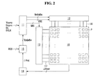
- FIG. 2 illustrates an organic light emitting display according to an example embodiment of the invention
- FIG. 3 illustrates a configuration of a degradation compensation circuit shown in FIG. 2 ;
- FIG. 4 is a graph showing stepwise adjustment of a compensation target depending on a degradation degree
- FIGS. 5 and 6 illustrate a first example of a compensation target adjustor
- FIGS. 7 and 8 illustrate a second example of a compensation target adjustor
- FIGS. 9 and 10 illustrate a third example of a compensation target adjustor
- FIGS. 11 and 12 illustrate a fourth example of a compensation target adjustor
- FIG. 13 illustrates a degradation compensation method of an organic light emitting display according to an example embodiment of the invention.
- Example embodiments of the invention will be described with reference to FIGS. 2 to 13 .
- FIG. 2 illustrates an organic light emitting display according to an example embodiment of the invention.
- an organic light emitting display includes a display panel 10 including pixels P which are arranged in a matrix form, a data driving circuit 12 for driving data lines 16 , a gate driving circuit 13 for driving gate line groups 17 , a timing controller 11 for controlling operations of the driving circuits 12 and 13 , a degradation sensing circuit 14 for sensing degradation of an organic light emitting diode (hereinafter, abbreviated to “OLED”) included in each of the pixels P, and a degradation compensation circuit 15 which modulates input digital video data and compensates for a luminance reduction resulting from the degradation of the OLEDs.
- OLED organic light emitting diode
- the display panel 10 includes the plurality of data lines 16 , the plurality of gate line groups 17 crossing the data lines 16 , and the plurality of pixels P respectively positioned at crossings of the data lines 16 and the gate line groups 17 .
- Each of the plurality of gate line groups 17 may include a scan pulse supply line for the supply of a scan pulse, an emission pulse supply line for the supply of an emission pulse, and a sensing pulse supply line for the supply of a sensing pulse.
- Each gate line group 17 may further include an initialization line for supplying an initialization voltage based on a structure of a pixel circuit.
- Each pixel P is connected to the data driving circuit 12 through the data lines 16 and is connected to the gate driving circuit 13 through the gate line groups 17 .
- Each pixel P may include an OLED, a driving thin film transistor (TFT) for controlling an amount of driving current flowing in the OLED based on a data voltage, at least one switching TFT, a storage capacitor, etc.
- the pixel P may have any known structure as long as it can sense a threshold voltage ⁇ Vsen of the OLED.
- the pixel P may be designed to have the same structure as a pixel disclosed in detail in Korean Patent Application Nos. 10-2009-0113974 (Nov. 24, 2009), 10-2009-0113979 (Nov. 24, 2009), and 10-2009-0123190 (Dec. 11, 2009) corresponding to the present applicant, and which are hereby incorporated by reference in their entirety.
- the timing controller 11 receives timing signals such as a vertical sync signal Vsync, a horizontal sync signal Hsync, a dot clock DCLK, and a data enable DE from a system board (not shown) and generates a source control signal SDC for controlling operation timing of the data driving circuit 12 and a gate control signal GDC for controlling operation timing of the gate driving circuit 13 based on the timing signals Vsync, Hsync, DCLK, and DE.
- timing signals such as a vertical sync signal Vsync, a horizontal sync signal Hsync, a dot clock DCLK, and a data enable DE from a system board (not shown) and generates a source control signal SDC for controlling operation timing of the data driving circuit 12 and a gate control signal GDC for controlling operation timing of the gate driving circuit 13 based on the timing signals Vsync, Hsync, DCLK, and DE.
- the timing controller 11 receives digital modulation data RmGmBm for the degradation compensation from the degradation compensation circuit 15 and arranges the digital modulation data RmGmBm in conformity with the display panel 10 .
- the timing controller 11 supplies the arranged digital modulation data RmGmBm to the data driving circuit 12 .
- the timing controller 11 produces programming data to be applied to the pixels P in a degradation sensing period of the OLEDs of the pixels P and supplies the programming data to the data driving circuit 12 .
- the programming data to be applied to the pixels P may be selected as a value suitable to sense the threshold voltage ⁇ Vsen of the OLEDs.
- the timing controller 11 may separately set an image display period, in which a display image is implemented in a state where the OLED is compensated for its degradation deviation through the data modulation, and a degradation sensing period, in which the threshold voltage ⁇ Vsen of the OLEDs is sensed.
- the degradation sensing period may be set to at least one frame period synchronized with on-timing of a driving power source or at least one frame period synchronized with off-timing of the driving power source.
- the degradation sensing period may be set to a vertical blank period between every two image display periods.
- the timing controller 11 may differently control operations of the data driving circuit 12 and the gate driving circuit 13 in the image display period and the degradation sensing period.
- the data driving circuit 12 converts the digital modulation data RmGmBm into the data voltage under the control of the timing controller 11 and supplies the data voltage to the data lines 16 .
- the data driving circuit 12 converts the programming data received from the timing controller 11 into a programming voltage under the control of the timing controller 11 and supplies the programming voltage to the data lines 16 .
- the gate driving circuit 13 includes a shift register and a level shifter and generates the scan pulse, the sensing pulse, and the emission pulse under the control of the timing controller 11 .
- the scan pulse is applied to the scan pulse supply line
- the emission pulse is applied to the emission pulse supply line
- the sensing pulse is applied to the sensing pulse supply line.
- the shift register constituting the gate driving circuit 13 may be directly formed on the display panel 10 in a Gate In Panel (GIP) manner.
- GIP Gate In Panel
- the degradation sensing circuit 14 senses the threshold voltage ⁇ Vsen of the OLEDs of the pixels P.
- the degradation sensing circuit 14 operates in the degradation sensing period under the control of the timing controller 11 .
- the degradation sensing circuit 14 may use a sensing method disclosed in detail in Korean Patent Application Nos. 10-2009-0113974 (Nov. 24, 2009), 10-2009-0113979 (Nov. 24, 2009), and 10-2009-0123190 (Dec. 11, 2009) corresponding to the present applicant, and which are hereby incorporated by reference in their entirety.
- the degradation sensing circuit 14 calculates an average luminance value (hereinafter referred to as “average degradation value”) ⁇ Avg due to the degradation based on the threshold voltage ⁇ Vsen of the OLEDs obtained by a sensing operation.
- average degradation value an average luminance value
- the average degradation value ⁇ Avg is an luminance index indicating a degradation degree throughout the entire area of the display panel 10 . As usage time passed (i.e., as the degradation of the OLED deepens), the average degradation value ⁇ Avg decreases.
- the degradation compensation circuit 15 receives the average degradation value ⁇ Avg from the degradation sensing circuit 14 . Each time the average degradation value ⁇ Avg is reduced by a previously determined reference value, the degradation compensation circuit 15 adjusts a compensation target, which is a criterion of the luminance compensation, based on the average degradation value ⁇ Avg.
- the degradation compensation circuit 15 modulates input digital video data RGB based on the adjusted compensation target to produce the digital modulation data RmGmBm.
- the degradation compensation circuit 15 may be embedded in the timing controller 11 .
- FIG. 3 illustrates a configuration of the degradation compensation circuit 15 shown in FIG. 2 .
- FIG. 4 is a graph showing stepwise adjustment of a compensation target depending on a degradation degree.
- the degradation compensation circuit 15 includes a compensation target adjustor 151 which adjusts the compensation target based on the average degradation value ⁇ Avg, and a data modulator 152 which modulates the input digital video data RGB based on the adjusted compensation target.
- the compensation target adjustor 151 reduces stepwise the compensation target in conformity with changes in the average degradation value ⁇ Avg, thereby reducing a luminance gap between the compensation target and a luminance subject to compensation. Because the average degradation value ⁇ Avg is defined by the average luminance value due to the degradation, the average degradation value ⁇ Avg is continuously reduced as usage time passed.
- FIG. 4 illustrates that the reference value is 5%, for example. The reference value may be set to other values. Furthermore, a stepwise adjustment width of the compensation target may be uniform or not-uniform. FIGS.
- FIG. 6 , 8 , and 10 illustrate that the stepwise adjustment width of the compensation target is uniform. It is a matter of course that a downward adjustment width of the compensation target in FIGS. 6 , 8 , and 10 may be not-uniform.
- FIG. 12 illustrates that the stepwise adjustment width of the compensation target gradually increases as the degradation of the OLED deepens. It is a matter of course that a downward adjustment width of the compensation target in FIG. 12 may be differently set.
- the compensation target adjustor 151 adjusts the compensation target depending on the degradation degree to reduce the luminance gap between the compensation target and the luminance subject to compensation. Hence, the compensation target adjustor 151 may minimize a compensation error and may improve a compensation performance without breaking a luminance balance and a color balance. The compensation target adjustor 151 may reduce power consumption required in the degradation compensation by adjusting the compensation target depending on the degradation degree and reducing an entire luminance of the screen of the display panel 10 .
- the data modulator 152 adds and subtracts a luminance compensation value determined depending on the adjusted compensation target to and from the input digital video data RGB to thereby produce the digital modulation data RmGmBm.
- a pixel having a luminance higher than the compensation target through the data modulation operation represents the luminance lower than an original luminance of the pixel
- a pixel having a luminance lower than the compensation target through the data modulation operation represents the luminance higher than an original luminance of the pixel. Hence, the luminance difference between the pixels is reduced.
- FIGS. 5 and 6 illustrate a first example of the compensation target adjustor 151 .
- the compensation target adjustor 151 may include a plurality of lookup tables LUT#1 to LUT#N, which are previously set. Different compensation target values and luminance compensation values based on the different compensation target values are previously stored in the lookup tables LUT#1 to LUT#N.
- the compensation target adjustor 151 selects one of the lookup tables LUT#1 to LUT#N based on the average degradation value ⁇ Avg received from the degradation sensing circuit 14 and changes stepwise the compensation target based on the average degradation value ⁇ Avg.
- the compensation target adjustor 151 selects the first lookup table LUT#1 when the average degradation value ⁇ Avg is 100%, selects the second lookup table LUT#2 when the average degradation value ⁇ Avg is 95%, and selects the third lookup table LUT#3 when the average degradation value ⁇ Avg is 90%. In other words, the compensation target adjustor 151 selects the different lookup table each time the average degradation value ⁇ Avg is reduced by the reference value (for example, 5%).
- the compensation target and the luminance compensation value are determined depending on the selected lookup table.
- the data modulator 152 adds and subtracts the luminance compensation value determined by the selected lookup table to and from the input digital video data RGB.
- FIGS. 7 and 8 illustrate a second example of the compensation target adjustor 151 .
- the compensation target adjustor 151 may include a plurality of numerical algorisms L 1 , L 2 , L 3 , . . . which are previously set.
- the numerical algorisms L 1 , L 2 , L 3 , . . . determine different compensation target values and luminance compensation values based on the different compensation target values depending on the average degradation value ⁇ Avg.
- the numerical algorisms L 1 , L 2 , L 3 , . . . may be determined by a functional equation to adopt one of average degradation coefficients b, b′, b′′, . . . , which are previously set depending on the average degradation value ⁇ Avg, as an offset value.
- the stepwise adjustment width of the compensation target depends on the offset value, and thus is determined depending on how the average degradation coefficients b, b′, b′′, . . . are set.
- ‘a’ indicates a compensation coefficient
- ‘x’ indicates a degradation value based on the threshold voltage ⁇ Vsen of the OLEDs.
- FIG. 7 illustrates that each of the numerical algorisms L 1 , L 2 , L 3 , . . . is defined by a linear function.
- the numerical algorisms L 1 , L 2 , L 3 , . . . are not limited thereto.
- the compensation target adjustor 151 selects one of the numerical algorisms L 1 , L 2 , L 3 , . . . based on the average degradation value ⁇ Avg received from the degradation sensing circuit 14 and changes stepwise the compensation target based on the average degradation value ⁇ Avg.
- the compensation target adjustor 151 selects the first numerical algorism L 1 when the average degradation value ⁇ Avg is 100%, selects the second numerical algorism L 2 when the average degradation value ⁇ Avg is 95%, and selects the third numerical algorism L 3 when the average degradation value ⁇ Avg is 90%. In other words, the compensation target adjustor 151 selects the different numerical algorism each time the average degradation value ⁇ Avg is reduced by the reference value (for example, 5%).
- the compensation target and the luminance compensation value are determined depending on the selected numerical algorisms.
- the data modulator 152 adds and subtracts the luminance compensation value determined by the selected numerical algorisms to and from the input digital video data RGB.
- FIGS. 9 and 10 illustrate a third example of the compensation target adjustor 151 .
- the compensation target adjustor 151 may include one lookup table, in which a reference luminance compensation value is previously stored, and an offset adjustor which adjusts an offset value of an output (i.e., the reference luminance compensation value) of the lookup table to change the compensation target.
- the offset adjustor adds one of the average degradation coefficients b, b′, b′′, . . . , which are previously set depending on the average degradation value ⁇ Avg, to the reference luminance compensation value output from the lookup table, thereby adjusting the offset value of the reference luminance compensation value.
- the stepwise adjustment width of the compensation target depends on the offset value, and thus is determined depending on how the average degradation coefficients b, b′, b′′, . . . are set.
- the compensation target adjustor 151 adjusts the offset value of the reference luminance compensation value based on the average degradation value ⁇ Avg received from the degradation sensing circuit 14 , thereby changing stepwise the compensation target based on the average degradation value ⁇ Avg.
- the compensation target adjustor 151 adds the first average degradation coefficient b to the offset value of the output (i.e., the reference luminance compensation value) of the lookup table.
- the compensation target adjustor 151 adds the second average degradation coefficient b′ to the offset value of the reference luminance compensation value of the lookup table.
- the compensation target adjustor 151 adds the third average degradation coefficient b′′ to the offset value of the reference luminance compensation value of the lookup table.
- the compensation target adjustor 151 changes the average degradation coefficient added to the output (i.e., the reference luminance compensation value) of the lookup table each time the average degradation value ⁇ Avg is reduced by the reference value (for example, 5%).
- the compensation target and a final luminance compensation value are determined.
- the data modulator 152 adds and subtracts the determined final luminance compensation value to and from the input digital video data RGB.
- FIGS. 11 and 12 illustrate a fourth example of the compensation target adjustor 151 .
- the compensation target adjustor 151 according to the fourth example is different from the compensation target adjustor 151 according to the third example in a function of the offset adjustor.
- An offset adjustor according to the fourth example adjusts the offset value of the reference luminance compensation value of the lookup table using the average degradation coefficients b, b′, b′′, . . . and degradation weighting coefficients d, d′, d′′, . . . , thereby gradually increasing the stepwise adjustment width of the compensation target as the degradation deepens.
- the compensation target adjustor 151 may include one lookup table, in which a reference luminance compensation value is previously stored, and an offset adjustor which adjusts an offset value of an output (i.e., the reference luminance compensation value) of the lookup table to change the compensation target.
- the offset adjustor adds one of the average degradation coefficients b, b′, b′′, . . . , which are previously set depending on the average degradation value ⁇ Avg, and one of the degradation weighting coefficients d, d′, d′′, . . . to the reference luminance compensation value output from the lookup table, thereby adjusting the offset value of the reference luminance compensation value.
- the stepwise adjustment width of the compensation target may gradually increase because the degradation weighting coefficients d, d′, d′′, . . . are additionally added to the offset value of the reference luminance compensation value.
- the compensation target adjustor 151 adjusts the offset value of the reference luminance compensation value based on the average degradation value ⁇ Avg received from the degradation sensing circuit 14 , thereby changing stepwise the compensation target based on the average degradation value ⁇ Avg.
- the compensation target adjustor 151 adds the first average degradation coefficient b and the first degradation weighting coefficient d to the offset value of the output (i.e., the reference luminance compensation value) of the lookup table.
- the compensation target adjustor 151 adds the second average degradation coefficient b′ and the second degradation weighting coefficient d′ to the offset value of the reference luminance compensation value of the lookup table.
- the compensation target adjustor 151 adds the third average degradation coefficient b′′ and the third degradation weighting coefficient d′′ to the offset value of the reference luminance compensation value of the lookup table.
- the compensation target adjustor 151 changes the average degradation coefficient and the degradation weighting coefficient added to the output (i.e., the reference luminance compensation value) of the lookup table each time the average degradation value ⁇ Avg is reduced by the reference value (for example, 5%).
- the compensation target and a final luminance compensation value are determined.
- the data modulator 152 adds and subtracts the determined final luminance compensation value to and from the input digital video data RGB.
- FIG. 13 illustrates a degradation compensation method of the organic light emitting display according to the embodiment of the invention.
- the degradation compensation method of the organic light emitting display senses the threshold voltage ⁇ Vsen of the OLEDs included in the pixels in step S 10 .
- the degradation compensation method calculates the average degradation value ⁇ Avg, which is defined by the average luminance value due to the degradation, based on the threshold voltage ⁇ Vsen of the OLEDs obtained by a sensing operation in step S 20 .
- the degradation compensation method decides whether or not the average degradation value ⁇ Avg is reduced by a previously determined reference value in step S 30 . Each time the average degradation value ⁇ Avg is reduced by the previously determined reference value as the result of a decision, the degradation compensation method adjusts the compensation target, which is a criterion of the luminance compensation, based on the average degradation value ⁇ Avg in step S 40 .
- the degradation compensation method adds and subtracts the luminance compensation value determined by the adjusted compensation target to and from the input digital video data to modulate the input digital video data in step S 50 .
- the organic light emitting display and the degradation compensation method thereof according to the embodiment of the invention adjusts the compensation target depending on the degradation degree of the OLEDs of the pixels to thereby reduce the luminance gap between the compensation target and the luminance subject to compensation. Hence, the compensation error is minimized, and the compensation performance may be improved without breaking the luminance balance and the color balance. Furthermore, the organic light emitting display and the degradation compensation method thereof according to the embodiment of the invention adjusts the compensation target depending on the degradation degree of the OLEDs to thereby reduce the entire luminance of the screen of the display panel. Hence, the power consumption required to compensate for the degradation of the OLEDs may be reduced.
Priority Applications (1)
| Application Number | Priority Date | Filing Date | Title |
|---|---|---|---|
| US14/968,475 US9779655B2 (en) | 2011-12-08 | 2015-12-14 | Organic light emitting display for luminance degradation compensation and a method thereof |
Applications Claiming Priority (2)
| Application Number | Priority Date | Filing Date | Title |
|---|---|---|---|
| KR10-2011-0131217 | 2011-12-08 | ||
| KR1020110131217A KR101470688B1 (ko) | 2011-12-08 | 2011-12-08 | 유기발광 표시장치 및 그의 열화보상방법 |
Related Child Applications (1)
| Application Number | Title | Priority Date | Filing Date |
|---|---|---|---|
| US14/968,475 Division US9779655B2 (en) | 2011-12-08 | 2015-12-14 | Organic light emitting display for luminance degradation compensation and a method thereof |
Publications (2)
| Publication Number | Publication Date |
|---|---|
| US20130147693A1 US20130147693A1 (en) | 2013-06-13 |
| US9230472B2 true US9230472B2 (en) | 2016-01-05 |
Family
ID=48571499
Family Applications (2)
| Application Number | Title | Priority Date | Filing Date |
|---|---|---|---|
| US13/679,595 Active 2033-12-25 US9230472B2 (en) | 2011-12-08 | 2012-11-16 | Organic light emitting display and degradation compensation method thereof |
| US14/968,475 Active 2032-12-09 US9779655B2 (en) | 2011-12-08 | 2015-12-14 | Organic light emitting display for luminance degradation compensation and a method thereof |
Family Applications After (1)
| Application Number | Title | Priority Date | Filing Date |
|---|---|---|---|
| US14/968,475 Active 2032-12-09 US9779655B2 (en) | 2011-12-08 | 2015-12-14 | Organic light emitting display for luminance degradation compensation and a method thereof |
Country Status (3)
| Country | Link |
|---|---|
| US (2) | US9230472B2 (zh) |
| KR (1) | KR101470688B1 (zh) |
| CN (1) | CN103165076B (zh) |
Cited By (4)
| Publication number | Priority date | Publication date | Assignee | Title |
|---|---|---|---|---|
| US20160189621A1 (en) * | 2014-12-29 | 2016-06-30 | Lg Display Co., Ltd. | Organic light emitting diode display device and driving method thereof |
| US10490127B2 (en) | 2016-07-07 | 2019-11-26 | Samsung Display Co., Ltd. | Organic light emitting display device and driving method thereof |
| US10964257B2 (en) * | 2019-05-22 | 2021-03-30 | Samsung Electronics Co., Ltd. | Display device |
| US11615750B2 (en) | 2021-05-14 | 2023-03-28 | Samsung Display Co., Ltd. | Display device and method of driving the same |
Families Citing this family (51)
| Publication number | Priority date | Publication date | Assignee | Title |
|---|---|---|---|---|
| KR101964458B1 (ko) * | 2012-12-10 | 2019-04-02 | 엘지디스플레이 주식회사 | 유기발광 표시장치 및 그의 열화보상방법 |
| KR102024828B1 (ko) | 2013-11-13 | 2019-09-24 | 엘지디스플레이 주식회사 | 유기발광표시장치 |
| CN103681772B (zh) * | 2013-12-27 | 2018-09-11 | 京东方科技集团股份有限公司 | 一种阵列基板和显示装置 |
| KR102126543B1 (ko) * | 2013-12-27 | 2020-06-24 | 엘지디스플레이 주식회사 | 유기 발광 다이오드 표시 장치의 데이터 처리 방법 및 장치 |
| CN103886835B (zh) * | 2014-02-10 | 2016-03-23 | 深圳市明微电子股份有限公司 | 解决动态屏行偏暗现象的方法、系统及驱动芯片、控制卡 |
| JP2015156002A (ja) * | 2014-02-21 | 2015-08-27 | 三星ディスプレイ株式會社Samsung Display Co.,Ltd. | 表示装置、および制御方法 |
| CN104021759A (zh) * | 2014-05-30 | 2014-09-03 | 京东方科技集团股份有限公司 | 一种显示器件的亮度补偿方法、亮度补偿装置及显示器件 |
| CN105225621B (zh) * | 2014-06-25 | 2020-08-25 | 伊格尼斯创新公司 | 提取有机发光器件的相关曲线的系统和方法 |
| KR102270460B1 (ko) * | 2014-09-19 | 2021-06-29 | 삼성디스플레이 주식회사 | 유기 발광 표시 장치 및 이의 열화 보상 방법 |
| KR102281008B1 (ko) * | 2014-09-24 | 2021-07-23 | 엘지디스플레이 주식회사 | 유기 발광 다이오드 표시 장치 |
| KR102264271B1 (ko) * | 2014-11-17 | 2021-06-15 | 엘지디스플레이 주식회사 | 유기발광 표시장치와 그 구동방법 |
| KR102320306B1 (ko) | 2014-11-17 | 2021-11-02 | 삼성디스플레이 주식회사 | 유기 발광 표시 장치 및 그 구동 방법 |
| KR102401884B1 (ko) | 2014-11-26 | 2022-05-26 | 삼성디스플레이 주식회사 | 신호 처리 장치 및 이를 포함하는 유기 발광 표시 장치 |
| KR102336090B1 (ko) | 2014-12-15 | 2021-12-07 | 삼성디스플레이 주식회사 | 유기 발광 표시 장치 및 이의 구동방법 |
| KR102297573B1 (ko) * | 2014-12-24 | 2021-09-06 | 엘지디스플레이 주식회사 | 컨트롤러, 소스 드라이버 집적회로, 표시장치 및 그 신호전송방법 |
| KR20160082752A (ko) * | 2014-12-29 | 2016-07-11 | 엘지디스플레이 주식회사 | 데이터 변환 장치와 이를 포함하는 유기발광다이오드 표시장치 |
| CN107111986B (zh) * | 2015-01-19 | 2020-06-23 | 夏普株式会社 | 显示装置以及其驱动方法 |
| KR20160092537A (ko) * | 2015-01-27 | 2016-08-05 | 삼성디스플레이 주식회사 | 유기 발광 표시 장치 및 이의 로고 영역 휘도 조절 방법 |
| KR102346523B1 (ko) * | 2015-01-27 | 2022-01-04 | 삼성디스플레이 주식회사 | 데이터 보상 장치 및 이를 포함하는 표시 장치 |
| KR102218531B1 (ko) * | 2015-01-29 | 2021-02-23 | 삼성디스플레이 주식회사 | 데이터 보상기 및 이를 포함하는 표시 장치 |
| CN104680979B (zh) * | 2015-03-23 | 2019-03-12 | 京东方科技集团股份有限公司 | Oled显示装置和用于矫正oled显示装置的残像的方法 |
| KR102335763B1 (ko) | 2015-04-03 | 2021-12-08 | 삼성디스플레이 주식회사 | 유기전계발광 표시장치 및 그의 구동방법 |
| KR102360222B1 (ko) * | 2015-06-16 | 2022-02-10 | 삼성디스플레이 주식회사 | 유기전계발광 표시장치 및 그의 구동방법 |
| KR102287907B1 (ko) * | 2015-06-22 | 2021-08-10 | 삼성디스플레이 주식회사 | 유기 발광 다이오드 표시 장치의 열화 보상기 |
| KR102485574B1 (ko) * | 2015-07-29 | 2023-01-09 | 삼성디스플레이 주식회사 | 표시 장치 및 이의 구동 방법 |
| KR102387789B1 (ko) * | 2015-08-31 | 2022-04-15 | 엘지디스플레이 주식회사 | 유기 발광 표시 장치 및 그 구동방법 |
| KR102502482B1 (ko) * | 2015-09-08 | 2023-02-23 | 삼성디스플레이 주식회사 | 표시 장치 및 표시 장치의 열화 보상 방법 |
| CN105206217B (zh) * | 2015-10-27 | 2018-02-06 | 京东方科技集团股份有限公司 | 显示处理方法、装置及显示器件 |
| KR102406705B1 (ko) * | 2015-10-30 | 2022-06-08 | 엘지디스플레이 주식회사 | 유기 발광 다이오드 표시 장치 |
| KR102447670B1 (ko) * | 2015-12-07 | 2022-09-28 | 삼성디스플레이 주식회사 | 열화 보상 장치, 이를 포함하는 유기 발광 표시 장치 및 유기 발광 표시 장치의 구동 방법 |
| KR20170124684A (ko) | 2016-05-02 | 2017-11-13 | 삼성디스플레이 주식회사 | 표시장치 및 그의 구동방법 |
| DE102016006890B4 (de) * | 2016-06-03 | 2022-06-30 | e.solutions GmbH | Technik zur Kompensation von Alterungserscheinungen einer Anzeigeeinheit und Computerprogrammprodukt zum Durchführen der Technik sowie Kraftfahrzeug mit einem System umfassend eine Steuervorrichtung und eine Anzeigeeinheit |
| CN105895056B (zh) * | 2016-06-17 | 2017-04-19 | 京东方科技集团股份有限公司 | 亮度补偿模型的建立方法、屏幕亮度的补偿方法及装置 |
| CN106847175B (zh) | 2017-03-01 | 2018-12-28 | 京东方科技集团股份有限公司 | 电致发光显示屏及其亮度均匀性补偿方法、系统 |
| KR102473221B1 (ko) * | 2017-08-24 | 2022-12-01 | 엘지디스플레이 주식회사 | 개인 몰입형 표시장치와 이의 구동방법 |
| KR102454169B1 (ko) * | 2017-09-15 | 2022-10-17 | 삼성디스플레이 주식회사 | 표시 장치 |
| KR102379191B1 (ko) * | 2017-09-25 | 2022-03-25 | 엘지디스플레이 주식회사 | 유기발광표시장치 및 이의 구동방법 |
| CN107799084B (zh) * | 2017-11-21 | 2019-11-22 | 武汉华星光电半导体显示技术有限公司 | 亮度补偿的装置及方法、存储器 |
| KR102593264B1 (ko) * | 2018-08-14 | 2023-10-26 | 삼성전자주식회사 | 디스플레이 드라이버 및 이를 포함하는 유기발광 표시장치 |
| CN109523950B (zh) * | 2018-12-13 | 2020-09-11 | 昆山国显光电有限公司 | 一种oled显示面板驱动电路及驱动方法 |
| CN109727578A (zh) * | 2018-12-14 | 2019-05-07 | 合肥鑫晟光电科技有限公司 | 显示装置的补偿方法、装置和显示设备 |
| CN110301000B (zh) * | 2019-01-04 | 2022-03-04 | 京东方科技集团股份有限公司 | 用于显示装置的亮度不均补偿的方法及相应的显示装置 |
| CN109658856B (zh) * | 2019-02-28 | 2021-03-19 | 京东方科技集团股份有限公司 | 像素数据补偿参数获取方法及装置、amoled显示面板 |
| KR102085516B1 (ko) * | 2019-05-01 | 2020-03-05 | 주식회사 티엘아이 | 효율적인 열화 보상 구조를 가지는 유기발광 디스플레이 장치 |
| CN110751923B (zh) * | 2019-11-28 | 2022-12-30 | 北京加益科技有限公司 | 混合老化补偿方法、装置、电子设备及可读存储介质 |
| JP2021096282A (ja) * | 2019-12-13 | 2021-06-24 | エルジー ディスプレイ カンパニー リミテッド | 発光表示装置 |
| CN112365862B (zh) * | 2020-11-09 | 2021-12-03 | 深圳市华星光电半导体显示技术有限公司 | 显示面板亮度调节方法及装置 |
| KR20220089813A (ko) * | 2020-12-21 | 2022-06-29 | 삼성디스플레이 주식회사 | 표시 장치 및 표시 장치의 구동 방법 |
| CN112863439B (zh) | 2021-01-21 | 2022-06-28 | 京东方科技集团股份有限公司 | 一种改善oled残像的方法、装置、显示装置及介质 |
| KR20230025596A (ko) * | 2021-08-13 | 2023-02-22 | 삼성디스플레이 주식회사 | 표시 장치 및 표시 장치의 구동 방법 |
| WO2023211453A1 (en) * | 2022-04-28 | 2023-11-02 | Hewlett-Packard Development Company, L.P. | Decay rates and luminance values of display panels |
Citations (5)
| Publication number | Priority date | Publication date | Assignee | Title |
|---|---|---|---|---|
| US20060007249A1 (en) * | 2004-06-29 | 2006-01-12 | Damoder Reddy | Method for operating and individually controlling the luminance of each pixel in an emissive active-matrix display device |
| US20110122119A1 (en) | 2009-11-24 | 2011-05-26 | Hanjin Bae | Organic light emitting diode display and method for driving the same |
| KR20110057531A (ko) | 2009-11-24 | 2011-06-01 | 엘지디스플레이 주식회사 | 유기발광다이오드 표시장치 및 그 구동방법 |
| KR20110066506A (ko) | 2009-12-11 | 2011-06-17 | 엘지디스플레이 주식회사 | 유기발광다이오드 표시장치 |
| US20140375701A1 (en) * | 2009-11-30 | 2014-12-25 | Ignis Innovation Inc. | System and methods for aging compensation in amoled displays |
Family Cites Families (8)
| Publication number | Priority date | Publication date | Assignee | Title |
|---|---|---|---|---|
| US20080122759A1 (en) * | 2006-11-28 | 2008-05-29 | Levey Charles I | Active matrix display compensating method |
| US7355574B1 (en) * | 2007-01-24 | 2008-04-08 | Eastman Kodak Company | OLED display with aging and efficiency compensation |
| KR100873076B1 (ko) * | 2007-03-14 | 2008-12-09 | 삼성모바일디스플레이주식회사 | 화소 및 이를 이용한 유기전계발광 표시장치 및 그의구동방법 |
| JP2008292649A (ja) * | 2007-05-23 | 2008-12-04 | Hitachi Displays Ltd | 画像表示装置 |
| KR100969769B1 (ko) * | 2008-01-21 | 2010-07-13 | 삼성모바일디스플레이주식회사 | 유기전계발광 표시장치 및 그의 구동방법 |
| JP2010243895A (ja) * | 2009-04-08 | 2010-10-28 | Seiko Epson Corp | 自発光表示装置および電子機器 |
| KR101679360B1 (ko) * | 2010-08-05 | 2016-11-25 | 삼성디스플레이 주식회사 | 계조전압 생성장치 및 방법, 및 유기전계발광표시장치 |
| CN101976545A (zh) * | 2010-10-26 | 2011-02-16 | 华南理工大学 | Oled显示器的像素驱动电路及其驱动方法 |
-
2011
- 2011-12-08 KR KR1020110131217A patent/KR101470688B1/ko active IP Right Grant
-
2012
- 2012-11-09 CN CN201210445172.0A patent/CN103165076B/zh active Active
- 2012-11-16 US US13/679,595 patent/US9230472B2/en active Active
-
2015
- 2015-12-14 US US14/968,475 patent/US9779655B2/en active Active
Patent Citations (6)
| Publication number | Priority date | Publication date | Assignee | Title |
|---|---|---|---|---|
| US20060007249A1 (en) * | 2004-06-29 | 2006-01-12 | Damoder Reddy | Method for operating and individually controlling the luminance of each pixel in an emissive active-matrix display device |
| US20110122119A1 (en) | 2009-11-24 | 2011-05-26 | Hanjin Bae | Organic light emitting diode display and method for driving the same |
| KR20110057531A (ko) | 2009-11-24 | 2011-06-01 | 엘지디스플레이 주식회사 | 유기발광다이오드 표시장치 및 그 구동방법 |
| KR20110057534A (ko) | 2009-11-24 | 2011-06-01 | 엘지디스플레이 주식회사 | 유기발광다이오드 표시장치 및 그 구동방법 |
| US20140375701A1 (en) * | 2009-11-30 | 2014-12-25 | Ignis Innovation Inc. | System and methods for aging compensation in amoled displays |
| KR20110066506A (ko) | 2009-12-11 | 2011-06-17 | 엘지디스플레이 주식회사 | 유기발광다이오드 표시장치 |
Cited By (5)
| Publication number | Priority date | Publication date | Assignee | Title |
|---|---|---|---|---|
| US20160189621A1 (en) * | 2014-12-29 | 2016-06-30 | Lg Display Co., Ltd. | Organic light emitting diode display device and driving method thereof |
| US10032414B2 (en) * | 2014-12-29 | 2018-07-24 | Lg Display Co., Ltd. | Organic light emitting diode display device and driving method thereof |
| US10490127B2 (en) | 2016-07-07 | 2019-11-26 | Samsung Display Co., Ltd. | Organic light emitting display device and driving method thereof |
| US10964257B2 (en) * | 2019-05-22 | 2021-03-30 | Samsung Electronics Co., Ltd. | Display device |
| US11615750B2 (en) | 2021-05-14 | 2023-03-28 | Samsung Display Co., Ltd. | Display device and method of driving the same |
Also Published As
| Publication number | Publication date |
|---|---|
| CN103165076B (zh) | 2015-08-19 |
| KR101470688B1 (ko) | 2014-12-08 |
| CN103165076A (zh) | 2013-06-19 |
| US20160098954A1 (en) | 2016-04-07 |
| US20130147693A1 (en) | 2013-06-13 |
| KR20130064552A (ko) | 2013-06-18 |
| US9779655B2 (en) | 2017-10-03 |
Similar Documents
| Publication | Publication Date | Title |
|---|---|---|
| US9779655B2 (en) | Organic light emitting display for luminance degradation compensation and a method thereof | |
| US10062324B2 (en) | Luminance control device and display device comprising the same | |
| US10991317B2 (en) | Display device and method for controlling luminance thereof | |
| KR101964458B1 (ko) | 유기발광 표시장치 및 그의 열화보상방법 | |
| US10930210B2 (en) | Organic light-emitting diode display capable of reducing kickback effect | |
| KR102018751B1 (ko) | 유기 발광 표시 장치 및 그의 구동 방법 | |
| JP5814334B2 (ja) | 有機発光表示装置及びその駆動方法 | |
| KR102146107B1 (ko) | 표시장치와 그 휘도 제어 방법 | |
| KR101960795B1 (ko) | 유기 발광 표시 장치 및 그의 구동 방법 | |
| US20080012804A1 (en) | Organic light emitting diode display and driving method thereof | |
| KR102106558B1 (ko) | 유기 발광 표시 장치 및 그의 구동 방법 | |
| US20140118410A1 (en) | Organic light emitting diode display and driving method thereof | |
| KR20130067092A (ko) | 유기발광 표시장치 및 그의 열화보상방법 | |
| KR102264270B1 (ko) | 유기발광 표시장치와 그 구동방법 | |
| KR20190081809A (ko) | 타일드 디스플레이와 그 휘도 보상 방법 | |
| KR20190074847A (ko) | 표시장치의 화질 보상 장치 및 방법 | |
| KR20190021760A (ko) | 전계 발광 시스템 및 그 기준전압 설정 방법 | |
| KR102217170B1 (ko) | 유기 발광 다이오드 표시 장치 | |
| CN115641814A (zh) | 显示装置及其驱动方法 | |
| JP2005300929A (ja) | 表示装置 | |
| KR20220092013A (ko) | 열화가 방지된 표시장치 및 이의 열화보상방법 | |
| US11862110B2 (en) | Data driver, electroluminescent display apparatus, and driving method thereof | |
| KR102237138B1 (ko) | 표시장치와 그 휘도 제어 방법 | |
| KR20230103681A (ko) | 디스플레이 장치 및 그 구동 방법 | |
| KR20230081043A (ko) | 디스플레이 장치 및 그 구동 방법 |
Legal Events
| Date | Code | Title | Description |
|---|---|---|---|
| AS | Assignment |
Owner name: LG DISPLAY CO., LTD., KOREA, REPUBLIC OF Free format text: ASSIGNMENT OF ASSIGNORS INTEREST;ASSIGNOR:BAE, HANJIN;REEL/FRAME:029323/0051 Effective date: 20121107 |
|
| FEPP | Fee payment procedure |
Free format text: PAYOR NUMBER ASSIGNED (ORIGINAL EVENT CODE: ASPN); ENTITY STATUS OF PATENT OWNER: LARGE ENTITY |
|
| STCF | Information on status: patent grant |
Free format text: PATENTED CASE |
|
| MAFP | Maintenance fee payment |
Free format text: PAYMENT OF MAINTENANCE FEE, 4TH YEAR, LARGE ENTITY (ORIGINAL EVENT CODE: M1551); ENTITY STATUS OF PATENT OWNER: LARGE ENTITY Year of fee payment: 4 |
|
| MAFP | Maintenance fee payment |
Free format text: PAYMENT OF MAINTENANCE FEE, 8TH YEAR, LARGE ENTITY (ORIGINAL EVENT CODE: M1552); ENTITY STATUS OF PATENT OWNER: LARGE ENTITY Year of fee payment: 8 |