US9225347B2 - Oscillator - Google Patents
Oscillator Download PDFInfo
- Publication number
- US9225347B2 US9225347B2 US14/226,828 US201414226828A US9225347B2 US 9225347 B2 US9225347 B2 US 9225347B2 US 201414226828 A US201414226828 A US 201414226828A US 9225347 B2 US9225347 B2 US 9225347B2
- Authority
- US
- United States
- Prior art keywords
- frequency
- output
- value
- digital value
- adjustment factor
- Prior art date
- Legal status (The legal status is an assumption and is not a legal conclusion. Google has not performed a legal analysis and makes no representation as to the accuracy of the status listed.)
- Active
Links
Images

Classifications
-
- H—ELECTRICITY
- H03—ELECTRONIC CIRCUITRY
- H03L—AUTOMATIC CONTROL, STARTING, SYNCHRONISATION OR STABILISATION OF GENERATORS OF ELECTRONIC OSCILLATIONS OR PULSES
- H03L7/00—Automatic control of frequency or phase; Synchronisation
- H03L7/06—Automatic control of frequency or phase; Synchronisation using a reference signal applied to a frequency- or phase-locked loop
- H03L7/08—Details of the phase-locked loop
- H03L7/099—Details of the phase-locked loop concerning mainly the controlled oscillator of the loop
-
- H—ELECTRICITY
- H03—ELECTRONIC CIRCUITRY
- H03L—AUTOMATIC CONTROL, STARTING, SYNCHRONISATION OR STABILISATION OF GENERATORS OF ELECTRONIC OSCILLATIONS OR PULSES
- H03L7/00—Automatic control of frequency or phase; Synchronisation
- H03L7/06—Automatic control of frequency or phase; Synchronisation using a reference signal applied to a frequency- or phase-locked loop
- H03L7/08—Details of the phase-locked loop
- H03L7/083—Details of the phase-locked loop the reference signal being additionally directly applied to the generator
-
- H—ELECTRICITY
- H03—ELECTRONIC CIRCUITRY
- H03L—AUTOMATIC CONTROL, STARTING, SYNCHRONISATION OR STABILISATION OF GENERATORS OF ELECTRONIC OSCILLATIONS OR PULSES
- H03L7/00—Automatic control of frequency or phase; Synchronisation
- H03L7/24—Automatic control of frequency or phase; Synchronisation using a reference signal directly applied to the generator
Definitions
- This disclosure relates to an oscillator that oscillates at a frequency corresponding to a frequency setting signal.
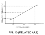
- FIG. 10 illustrates an exemplary relationship between the control voltage and the oscillation frequency.
- a variable width of the oscillation frequency depends on a linear curve area between a voltage and a capacitance of the varicap diode.
- it is difficult to perform an accurate frequency control and obtain high frequency stability because of some problems such as instability of an analog DC voltage or an output noise problem caused by a noise in a control signal line.
- a cost of the device tends to increase.
- an allowable frequency change ratio may have an order of “10 ⁇ 9 .” Such a requirement is not easy to satisfy.
- Japanese Unexamined Patent Application Publication No. 2012-170050 there is discussed a method of adjusting an oscillation frequency by generating a reference pulse input to a phase-locked loop (PLL) using a direct digital synthesizer (DDS) and inputting a digital value of a frequency setting value corresponding to the oscillation frequency of an oscillation circuit portion into the DDS.
- a user may desire to set a frequency with high accuracy within a usable range of the oscillation frequency allowed to the user or obtain a high resolution in the frequency setting.
- a variable frequency range desired by a user may be different case by case.
- a manufacturer may desire to suppress a circuit size as small as possible while there is a request for generalizing a product hardware configuration and obtaining a high frequency setting resolution.
- an oscillator configured to receive a frequency setting value input to an oscillation circuit portion and obtain a frequency output corresponding to the frequency setting value from the oscillation circuit portion, including: a setting value output portion that outputs a value for designating the frequency setting value as a digital value; an interpolation circuit portion that performs interpolation for a digital value of lower-order bits out of the digital value output from the setting value output portion; and an adder that adds an output value of the interpolation circuit portion and a digital value of higher-order bits out of the digital value output from the setting value output portion to output an addition value for designating the frequency setting value, wherein a signal output from the interpolation circuit portion is sequential data having first and second values different from each other and output in synchronization with a clock signal, and output counts of the first and second values are determined based on a ratio corresponding to the digital value of the lower-order bits.
- the value for designating the frequency setting value is output as a digital value. Therefore, unlike a case where a frequency is set based on an analog DC voltage, it is possible to address problems such as instability of a voltage or a noise problem in the output caused by a noise of a control signal line. Accordingly, it is possible to perform an accurate frequency control and obtain high frequency stability.
- the digital value for designating the frequency setting value is divided into higher-order bits and lower-order bits, and first and second values different from each other are output in synchronization with a clock signal.
- the first and second values are added to the higher-order bits, and each of the output counts of the first and second values is determined based on a ratio corresponding to the digital value of lower-order bits. Therefore, roughly speaking, even when the resolution of the setting frequency of the higher-order bits is set to, for example, “1 ppm,” the setting frequency changes, for example, between a value obtained by adding the first value and a value obtained by adding the second value for one second with respect to a value determined by “1 ppm” chopping.
- the setting frequency for one second can be regarded as an average of the addition values.
- the oscillator outputs a frequency of 10 MHz, and one bit of the higher-order bits changes from “10000000 Hz” to “10000010 Hz.”
- the first value is set to “+1”
- the second value is set to “4”
- the ratio between the output counts of the first and second values is set to 75%
- the ratio between the output counts of the first and second values refers to a percentage of “(output count of first value)/(output count of the first value+output count of second value),” for example, for one second.
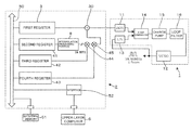
- FIG. 1 is a block diagram illustrating the entire configuration of an oscillator according to an embodiment disclosed here.
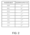
- FIG. 2 is an explanatory diagram illustrating an input/output relationship of a part of registers of a variable width setting portion.
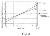
- FIG. 3 is a characteristic diagram illustrating a relationship between a digital value corresponding to a frequency adjustment factor and a change rate with respect to a normal frequency.
- FIG. 4 is an explanatory diagram obtained by matching data and addresses of registers used in the embodiment disclosed here.
- FIG. 5 is a block diagram illustrating an interpolation circuit portion used in the embodiment disclosed here.
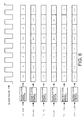
- FIG. 6 is a timing chart illustrating a relationship between a lower-order 8-bit value input to the interpolation circuit portion and an output value from the interpolation circuit portion.
- FIG. 7 is an explanatory diagram illustrating an output adjustment value of a voltage-controlled oscillator when the lower-order 8-bit value input to the interpolation circuit portion is set to “+32”.
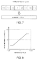
- FIG. 8 is a characteristic diagram illustrating an input/output relationship of the interpolation circuit portion.
- FIG. 9 is a circuit diagram illustrating another embodiment of this disclosure.
- FIG. 10 is a characteristic diagram illustrating a relationship between an oscillation frequency (output frequency) and a control voltage of an oscillator of the related art.
- FIG. 1 is a block diagram illustrating the entire configuration according to an embodiment disclosed here.
- the oscillator has a frequency synthesizer that output a frequency signal corresponding to a setting frequency.
- the frequency synthesizer includes an oscillation circuit portion 1 and a microcontroller 2 that outputs parameters necessary in the operation of the oscillation circuit portion 1 and serves as a controller for controlling the oscillation circuit portion 1 .
- the oscillation circuit portion 1 has a direct digital synthesizer (DDS) 11 .
- the DDS 11 receives frequency data (digital value) as a frequency setting signal and outputs a frequency signal corresponding to the frequency data.
- frequency data digital value
- a DDS that generates a sawtooth wave corresponding to the frequency data based on a digital value and outputs a rectangular wave whenever a negative digital value changes to a positive digital value (zero-cross point) out of the training digital values of the sawtooth wave.
- the frequency signal as a rectangular wave output from the DDS 11 is a reference clock. Therefore, the DDS 11 serves as a reference clock output portion. Meanwhile, an output of the voltage-controlled oscillator 12 as a part of the oscillation circuit portion 1 is divided by a divider 13 , so that a phase of the pulse output from the divider 13 and a phase of the reference clock are compared in a phase comparator 14 . A phase difference as the comparison result of the phase comparator 14 changes to an analog value using a charge pump 15 , and the analog signal is input to the loop filter 16 and is then integrated therein. In addition, the output of the loop filter 16 is input to the voltage-controlled oscillator 12 as a control voltage, and the control is performed to stabilize a phase-locked loop (PLL).
- PLL phase-locked loop
- a frequency corresponding to the frequency of the reference clock for example, in this example, a pulse signal having a frequency obtained by multiplying “N” (where “N” denotes a denominator of a division ratio) by the frequency of the reference clock is output as the output signal of the frequency synthesizer from the voltage-controlled oscillator 12 .
- the microcontroller 2 has a functionality of setting a frequency of the frequency synthesizer.
- the frequency synthesizer according to an embodiment disclosed here is configured to change a normal frequency determined by the manufacturer within a variable width set by the manufacturer.
- the variable width is expressed as a ratio (ppm) with respect to the normal frequency.
- the variable width is set to, for example, a ratio with the same negative and positive widths from the normal frequency.
- the variable width may be expressed as “normal frequency ⁇ 5 ppm.” Therefore, a user of the frequency synthesizer can adjust a frequency within this variable width range.
- a manufacturer of the frequency synthesizer sets the variable width in response to a user's request.
- Reference numeral “3” denotes a first register corresponding to a normal frequency output portion.
- the first register 3 sets the normal frequency as, for example, a 32-bit digital value (digital data).
- Reference numeral “41” denotes a second register as a frequency adjustment factor output portion.
- the second register 41 sets a frequency adjustment factor as a 24-bit digital value (digital data) expressed as 2's complement.
- the second register 41 corresponds to a frequency setting value output portion in this example.
- the frequency adjustment factor is to allow a user to set a ratio with respect to the normal frequency out of the variable width range set by a manufacturer. If this frequency adjustment factor is determined, a frequency corresponding to this ratio is added to the normal frequency as described below so that its addition value becomes frequency data as a frequency setting signal.
- An interpolation processing portion 8 for performing interpolation for the digital value output from the second register 41 is provided in rear of the second register 41 .
- the interpolation processing portion 8 is omitted before the interpolation processing portion 8 is described. Then, the interpolation processing portion 8 will be described in detail.
- the microcontroller 2 is provided with a gain output portion for setting a gain for the frequency adjustment factor set by the second register 41 .
- the gain output portion includes a third register 42 corresponding to a first gain output portion for setting a first gain G 1 and a fourth register 43 corresponding to a second gain output portion for setting a second gain G 2 .
- Reference numerals “ 44 ” and “ 45 ” denote multipliers.
- the gains G 1 and G 2 are determined such that the minimum value of the frequency adjustment factor set by the second register 41 corresponds to a lower limit (for example, “ ⁇ 5 ppm”) of the variable width, and the maximum value of the frequency adjustment factor set by the second register 41 corresponds to an upper limit (for example, “+5 ppm”) of the variable width. That is, as the frequency adjustment factor is shifted from the minimum value to the maximum value, a value of “frequency adjustment factor ⁇ G 1 ⁇ G 2 ” changes, for example, from “ ⁇ 5 ppm” to “+5 ppm.”
- the first gain G 1 is an 8-bit digital value, for example, expressed as 2′ complement.
- the second gain G 2 is a value for a rounding processing (multiplication of 2′, where “n” denotes any natural number) for a value obtained by multiplying the first gain G 1 by the frequency adjustment factor.
- the fourth register 43 receives a 3-bit digital value as an input, selects a value corresponding to the input value out of a set of values ⁇ 2 0 , 2 ⁇ 3 , 2 ⁇ 6 , 2 ⁇ 8 , 2 ⁇ 9 , 2 ⁇ 10 , 2 ⁇ 11 , and 2 ⁇ 12 ⁇ as the gain G 2 , and outputs the result.
- a relationship between the 3-bit digital value and the gain G 2 is illustrated in FIG. 2 .
- the frequency adjustment factor, the variable width, and the gains G 1 and G 2 will be described in more detail. Assuming that the normal frequency is set to “38.88 MHz,” the digital value corresponding to this normal frequency is “128792027777,” and the variable width is set to “ ⁇ 5 ppm,” a digital value of the first register 3 corresponding to “5 ppm” of “38.88 MHz” is “643960.” Since a 24-bit maximum value expressed as 2's complement in the second register 41 is “8388608-1,” it is possible to set to the variable width to “ ⁇ 5 ppm” by obtaining the gains G 1 and G 2 satisfying a condition that the output value of the multiplier 45 becomes “643960” when the 24-bit digital value is at maximum. In this case, the gain G 1 becomes “79,” and the gain G 2 becomes “2 ⁇ 10 .”
- Reference numeral “ 30 ” denotes an adder.
- the adder 30 adds the digital value corresponding to the normal frequency set in the first register 3 and the digital value from the multiplier 45 .
- the digital value (frequency setting data) obtained from the adder 30 is obtained by subtracting the frequency (“38.88 MHz” ⁇ “5/1,000,000”) corresponding to “5 ppm” from “38.88 MHz.”
- the frequency adjustment factor output portion 41 sets “8388608-1” which is the maximum value
- the digital value (frequency setting data) obtained from the adder 30 becomes a value obtained by adding or subtracting the frequency (38.88 MHz ⁇ 5/1,000,000) corresponding to “5 ppm” to or from the frequency of “38.88 MHz.”
- FIG. 3 illustrates a frequency adjustment factor (ratio of the frequency with respect to the normal frequency) when the digital value set by the frequency adjustment factor output portion 41 changes from the minimum value to the maximum value.
- the variable width is set to “ ⁇ 5 ppm.”
- the variable width is set to “ ⁇ 7 ppm.”
- the microcontroller 2 is connected to a non-volatile memory, for example, an external memory 51 including an electrically erasable programmable ROM (EEPROM).
- Reference numeral “ 50 ” denotes a bus.
- the microcontroller 2 has an interface 2 capable of steady communication with an upper-layer computer 6 .
- a standard of the interface 52 may include, for example, “I2C interface” or “RS232” as a standard specification of a serial interface. It is noted that the interface 52 may also be a parallel interface.
- the external memory 51 stores setup information of each oscillator.
- the setup information contains various parameters necessary in the oscillation circuit portion 1 , a part number, and the like.
- the setup information also contains the digital values stored in the first to fourth registers 3 , 41 , 42 , and 43 .
- the setup information is written to the external memory 51 from an upper-layer computer 6 using an interface 52 by a manufacturer.
- addresses allocated to the first to fourth registers 3 , 41 , 42 , and 43 match addresses allocated to the normal frequency in the external memory 51 , the frequency adjustment factor, the first and second gains G 1 and G 2 .
- the address of the external memory 51 allocated to the normal frequency is set to “A2”
- the address allocated to the first register 3 is also “A2.”
- FIG. 4 is a schematic diagram illustrating a table representing a matching relationship between the address of the external memory 51 and the stored data.
- FIG. 5 is a block diagram illustrating the interpolation processing portion 8 .
- the interpolation processing portion 8 includes an input port IN that receives a 32-bit digital value and an interpolation circuit portion 81 that receives a 8-bit digital value having an order lower than that of the “32 bits” and outputs sequential data containing a group of numbers as a digital signal training in a sequential manner corresponding to the input digital value.
- the group of numbers refers to a signal training in a sequential manner including first and second different values output in response to a clock signal at a predetermined time.
- the adder 82 is a circuit configured to add a group of numbers output from the interpolation circuit portion 81 and a 24-bit digital value having an order higher than the “32 bit.”
- the output port OUT outputs a 24-bit digital value.
- the interpolation circuit portion 81 includes a delta-sigma circuit portion that generates a pulse width modulation (PWM) signal for maintaining an average duty ratio at a value corresponding to the 8 bit digital value for a predetermined time and a circuit portion configured to output the group of numbers in response to the PWM signal.
- the group of numbers includes a 2-bit digital value “01” (decimal number “+1”) as 2's complement and a digital value “11” (decimal number “ ⁇ 1”) as 2's complement.
- PWM pulse width modulation
- the timing that the interpolation circuit portion 81 outputs “11” or “01” is synchronized with the timing that the adder 82 performs addition.
- the clock pulse for outputting each of the group of numbers from the interpolation circuit portion 81 is commonalized with the clock for performing the addition.
- the functionality of the interpolation processing portion 8 will be described. For example, it is assumed that a resolution of the frequency adjustment factor in the 24-bit digital value output from the second register 41 is set to 15 ppt/bit when the interpolation processing portion 8 is not provided. In this case, if the 24-bit digital value output from the second register 41 changes to “0”, “1”, “2”, “3”, . . . , and so on in a decimal expression, the frequency adjustment factor changes to 0 ppt, 15 ppt, 30 ppt, 45 ppt, . . . , and so on. In comparison, if the interpolation processing portion 8 receives the 32-bit digital value and outputs the 24-bit frequency adjustment factor as described above, the 24-bit digital value is incremented or decremented by “1.”
- the addition value of the adder 82 becomes “1” or “3.” If the aforementioned ratio ⁇ (output count of “01”)/(output count of “01”+output count of “11”) ⁇ between the 2-bit digital value “01” (decimal number “+1”) as 2's complement and the digital value “11” (decimal number “ ⁇ 1”) as 2's complement output from the interpolation circuit portion 81 is set to 50%, the adder 82 alternately outputs “1” and “3.” For this reason, for example, the voltage-controlled oscillator 12 outputs a pulse of the oscillation frequency corresponding to the frequency adjustment factor between “15 ppt” and “45 ppt” for one second. This is substantially equivalent to the frequency adjustment factor of 30 ppt. The inventors recognized that there is no spurious result such as an adverse effect in the output of the voltage-controlled oscillator 12 even when the setting is made as described above.
- the parameters include a normal frequency, gains G 1 and G 2 , and the like as described above.
- the setting of the normal frequency is performed as follows. A digital value as a frequency setting signal is input from the first register 3 to the DDS 11 of the oscillation circuit portion 1 , and an output frequency of the oscillation circuit portion 1 is measured using a frequency measurement device. Then, the digital value when the output frequency reaches the normal frequency is written to the external memory 51 as a setting value of the normal frequency. In this case, the second register 41 stores zero as the digital value.
- the gain G 1 of the third register 42 and the gain G 2 of the fourth register 43 are determined as described in detail in the aforementioned example, in which the normal frequency is “38.88 MHz,” and the digital value corresponding to the normal frequency is “128792027777.”
- a manufacturer determines a variable width (variable ratio) with respect to the normal frequency, for example, depending on a user's request, and the gains G 1 and G 2 are determined depending on the variable width.
- Such a value is input to the interface 52 as a serial signal from the upper-layer computer 6 .
- the serial signal is converted into a parallel signal and is written to the external memory 51 .
- a full range of the digital value stored in the second register 41 corresponds to a variable width, for example, ⁇ 5 ppm. Accordingly, it is possible adjust the output frequency by adjusting this digital value, for example, as illustrated in FIG. 3 .
- a manufacture may set the frequency adjustment factor to zero, and a user may set the out frequency to a desired value within a range of the variable width set by the manufacturer.
- a user rewrites the data of the second register 41 as a necessary frequency adjustment factor using the interface 52 from the upper-layer computer 6 .
- the frequency adjustment factor to be written to the second register 41 may be once written to the external memory 51 from the upper-layer computer 6 using the interface 52 and then read to the second register 41 when power is turned on.
- the parameters in the external memory 51 are read and written to the corresponding register based on a program stored in the microcontroller 2 .
- a digital value corresponding to the normal frequency is output from the first register 3 .
- the digital value stored in the second register 41 can be adjusted to any value by a user using the interface 52 , so that the digital value corresponding to the adjustment ratio with respect to the normal frequency is output.
- the gains G 1 and G 2 are multiplied to the digital value corresponding to the adjustment ratio, so that a digital value corresponding to the frequency to be adjusted with respect to the normal frequency is obtained.
- the adder 30 adds this digital value and the digital value corresponding to the normal frequency, and the resulting addition value is input to the DDS 11 of the oscillation circuit portion 1 as a frequency setting signal. Then, a desired output frequency is obtained from the oscillation circuit portion 1 by performing the operation as described above.
- FIG. 6 illustrates a state that the frequency adjustment factor as an adjustment ratio with respect to the normal frequency is output based on the 32-bit digital value output from the second register 41 .
- FIG. 6 is illustrated schematically for intuitive understanding.
- FIG. 6 illustrates a case where the decimal number P 1 of the 8-bit digital value input to the interpolation circuit portion 81 is set to the maximum value “128,” a case where the decimal number P 1 is set to “64,” “32,” “0,” and “ ⁇ 64,” and a case where the decimal number P 1 is set to the minimum value “ ⁇ 128.”
- the clock pulse located in the top is to set a timing for outputting a 2-bit digital value “01” (decimal number “+1”) as 2's complement or a digital value “11” (decimal number “ ⁇ 1”) as 2's complement is output from the interpolation circuit portion 81 .
- the interpolation circuit portion 81 outputs “+1” and “ ⁇ 1” at a ratio corresponding to the lower-order 8-bit value output from the second register 41 .
- the aforementioned ratio becomes 37.5%, so that “+1” is output five times, and “ ⁇ 1” is output three times for one second.
- “ ⁇ 1” is output when a distribution degree of a sequence of “+1” and “ ⁇ 1” becomes at maximum.
- FIG. 7 illustrates sequential data obtained by expressing the addition value of the adder 8 using the frequency adjustment factor (ppt).
- the output frequency of the oscillation circuit portion is set in the unit of 1 ⁇ 8 second, and the voltage-controlled oscillator 12 outputs a frequency obtained by adding “+15 ppt” to the normal frequency and a frequency obtained by adding “ ⁇ 15 ppt” to the normal frequency depending on the sequential data of FIG. 7 .
- an average of the oscillation frequency for one second becomes a value obtained by adding “9.375 ppt” to the normal frequency. That is, it is recognized that it is possible to set a frequency with a resolution higher than that determined by a 24-bit digital value.
- FIG. 8 illustrates an exemplary relationship between a digital value input to the interpolation circuit portion 81 and a ratio between the output counts of “+1” and “ ⁇ 1” described above.
- the oscillation circuit may include an oven-controlled crystal oscillator (OCXO) or a temperature-compensated crystal oscillator (TCXO).
- OXO oven-controlled crystal oscillator
- TCXO temperature-compensated crystal oscillator
- a compensation signal corresponding to a detection result of a temperature detector is added to the frequency setting signal (output signal from the adder 30 ) obtained as described above, and the result is input to the DDS 11 .
- the value for designating the frequency setting value is output as a 24-bit digital value. Therefore, it is possible to address problems such as voltage instability generated when a frequency is set based on an analog DC voltage or an output noise problem caused by a noise in a control signal line. Accordingly, it is possible to perform an accurate frequency control and obtain high frequency stability.
- the value for designating the frequency setting value is output as a 36-bit digital value, this digital value is divided into higher-order bits and lower-order bits, and the first value “+1” and the second value “ ⁇ 1” different from each other is output in synchronization with a clock signal.
- the first and second values are added to the higher-order bits, and the output counts of the first and second values are determined based on the aforementioned ratio corresponding to the digital value of the lower-order bits. Therefore, as described above, it is possible to obtain a resolution higher than that of the frequency setting value set by a 24-bit digital value while the 24-bit digital value is used. As a result, it is possible to obtain a high resolution for the setting frequency with a small number of bits. Therefore, it is possible to suppress an increase of a circuit size.
- the 32-bit digital value as the value for designating the frequency setting value is output from the second register 41 as a setting value output portion.
- a parameter for the interpolation value corresponding to the lower-order 8-bit digital value is output from the interpolation circuit portion 81 .
- the number of bits (value for designating the frequency setting value) for obtaining a resolution of the setting frequency of the frequency synthesizer is not limited to 32 bits. Preferably, the number of bits is equal to or larger than 16 bits.
- first and second values output from the interpolation circuit portion 81 are not limited to “ ⁇ 1” and “+1,” but may be set to other values if the same effects of this disclosure can be obtained.
- the first and second values may have the same sign, or the absolute values of the first and second values may be different.
- a clock for latching the timing of outputting the first and second values from the interpolation circuit portion 81 has a frequency of 8 Hz in the aforementioned description.
- the clock may be set to, for example, 26.1 MHz.
- the operational clock of the DDS 11 may be set to, for example, 26.1 MHz, and the normal frequency may be set to, for example, 38.88 MHz.
- a digital value corresponding to a normal frequency is output using the first register 3 as a normal frequency output portion, and a digital value for a frequency adjustment factor with respect to the normal frequency is generated as a value obtained by multiplying a gain and a frequency adjustment factor expressed as a frequency ratio.
- This multiplication value is added to the normal frequency, and the result is set as a frequency setting signal.
- the gain is determined such that a variable range of the digital value as the frequency adjustment factor matches a frequency variable width expressed as a frequency ratio. Therefore, according to the embodiment disclosed here, for example, a manufacturer can set the variable width expressed as the frequency ratio depending on a use range of the oscillation frequency using an upper-layer computer 6 , and a user can set a frequency with high resolution within the variable width. Accordingly, it is possible to cope with various specifications for a frequency adjustment range without changing a hardware configuration.
- the embodiment disclosed here is suitably applied to a system that requires high frequency stability and highly stable frequency control, such as a global positioning system (GPS). Furthermore, since the frequency adjustment factor is determined by setting a digital value in the register 41 , it is possible to obtain excellent linearity between a frequency setting input value and a frequency setting signal input to the oscillation circuit portion and excellent linearity between a frequency setting input value and an output frequency, compared to a case where a frequency is set using an analog circuit.
- GPS global positioning system
- a method of writing a digital value to each of the registers 3 , 41 , 42 , and 43 is not limited to a method of reading from the external memory 51 .
- the digital value may be directly written from an upper-layer computer using an interface 52 .
- variable frequency width a user may change the variable frequency width.
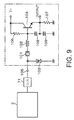
- FIG. 9 illustrates an example in which a Colpitts oscillation circuit is employed as the oscillation circuit portion.
- This circuit includes a crystal vibrator 101 , an inductor 102 , an oscillation portion having, for example, a varicap diode 103 as a voltage-controlled variable capacitance element, and a transistor 104 as an amplifier.
- a capacitance of the varicap diode 103 changes to set the oscillation frequency by inputting an analog control voltage to a control input terminal 105 .
- Reference numerals 106 and 107 denote resistors
- reference numerals 108 and 109 denote capacitors.
- Reference numeral 7 denotes an oscillation circuit portion.
- a digital-analog converter 71 is provided between an output terminal (output terminal of the adder 30 ) of the frequency setting signal of the microcontroller 2 of FIG. 1 and the control input terminal 105 .
- the digital-analog converter 71 converts the frequency setting signal as a digital value into an analog signal and input the analog signal into the control input terminal 105 .
- the effects similar to those described in the aforementioned embodiment can be obtained.
- the oscillation circuit portion may include any other oscillation circuit such as a Pierce circuit, a Clapp circuit, and a Butler circuit.
- variable frequency width expressed as a frequency ratio may have a different width between the positive and negative sides with respect to the normal frequency instead of the same width.
- the variable width is set to “ ⁇ 5 ppm” with respect to the normal frequency.
- the variable width may be set to, for example, “ ⁇ 4 ppm” and “+6 ppm” with respect to the normal frequency.
- Such a frequency setting may be performed, for example, by providing a subsidiary register in addition to the configuration of FIG. 1 .
- a digital value corresponding to “+1 ppm” may be set in the subsidiary register, and the digital value from the subsidiary register may be added to the digital value output from the second register 41 , so that the gains G 1 and G 2 are multiplied to the addition value.
- the digital value of the second register 41 changes from the minimum value to the maximum value, a variable width of “ ⁇ 4 ppm” to “+6 ppm” is obtained because the frequency adjustment factor of “+1 ppm” is added.
- the register is used as the normal frequency output portion, the frequency adjustment factor output portion, and the gain output portion in the embodiment of FIG. 1 , other memory elements such as a random access memory (RAM) may also be employed without limiting to the register.
- RAM random access memory
- a crystal vibrator is employed as an oscillator in the oscillation circuit portion in the embodiment disclosed here, other elements such as an LC oscillation circuit (including an inductor and a conductor) may also be employed as the oscillator.
Landscapes
- Stabilization Of Oscillater, Synchronisation, Frequency Synthesizers (AREA)
- Oscillators With Electromechanical Resonators (AREA)
Applications Claiming Priority (2)
| Application Number | Priority Date | Filing Date | Title |
|---|---|---|---|
| JP2013-074621 | 2013-03-29 | ||
| JP2013074621 | 2013-03-29 |
Publications (2)
| Publication Number | Publication Date |
|---|---|
| US20140292416A1 US20140292416A1 (en) | 2014-10-02 |
| US9225347B2 true US9225347B2 (en) | 2015-12-29 |
Family
ID=51600368
Family Applications (1)
| Application Number | Title | Priority Date | Filing Date |
|---|---|---|---|
| US14/226,828 Active US9225347B2 (en) | 2013-03-29 | 2014-03-27 | Oscillator |
Country Status (4)
| Country | Link |
|---|---|
| US (1) | US9225347B2 (enExample) |
| JP (1) | JP6298686B2 (enExample) |
| CN (1) | CN104079296B (enExample) |
| TW (1) | TWI596889B (enExample) |
Families Citing this family (3)
| Publication number | Priority date | Publication date | Assignee | Title |
|---|---|---|---|---|
| JP6564250B2 (ja) * | 2015-06-12 | 2019-08-21 | 日本電波工業株式会社 | 発振装置 |
| JP6823268B2 (ja) * | 2016-03-11 | 2021-02-03 | 株式会社ソシオネクスト | 分周回路、デマルチプレクサ回路、及び半導体集積回路 |
| US10128783B2 (en) * | 2016-05-31 | 2018-11-13 | Infineon Technologies Ag | Synchronization of internal oscillators of components sharing a communications bus |
Citations (10)
| Publication number | Priority date | Publication date | Assignee | Title |
|---|---|---|---|---|
| US5079521A (en) * | 1989-11-22 | 1992-01-07 | Stc Plc | Fractional-n frequency synthesizer using delta-sigma modulator in divider control circuit |
| US5563535A (en) * | 1994-11-29 | 1996-10-08 | Microunity Systems Engineering, Inc. | Direct digital frequency synthesizer using sigma-delta techniques |
| US6234658B1 (en) * | 1996-06-07 | 2001-05-22 | Duality Semiconductor, Inc. | Method and apparatus for producing signal processing circuits in the delta sigma domain |
| US20020043992A1 (en) * | 1999-03-17 | 2002-04-18 | Mccune Earl W. | Sigma-delta-based frequency synthesis |
| US6717998B2 (en) * | 1999-12-13 | 2004-04-06 | Matsushita Electric Industrial Co., Ltd. | Frequency synthesizer apparatus equipped with fraction part control circuit, communication apparatus, frequency modulator apparatus, and frequency modulating method |
| US20050073368A1 (en) * | 2001-12-14 | 2005-04-07 | Owen David Paul | Low noise synthesiser |
| US7577695B2 (en) * | 2004-07-22 | 2009-08-18 | Auburn University | High-order delta-sigma noise shaping in direct digital frequency synthesis |
| JP2012170050A (ja) | 2011-01-28 | 2012-09-06 | Nippon Dempa Kogyo Co Ltd | 発振装置 |
| JP2012195932A (ja) | 2011-02-28 | 2012-10-11 | Nippon Dempa Kogyo Co Ltd | 発振装置 |
| JP2013098872A (ja) | 2011-11-02 | 2013-05-20 | Nippon Dempa Kogyo Co Ltd | 発振器 |
Family Cites Families (5)
| Publication number | Priority date | Publication date | Assignee | Title |
|---|---|---|---|---|
| JP3395529B2 (ja) * | 1996-06-28 | 2003-04-14 | 三菱電機株式会社 | 周波数シンセサイザ |
| JP2000304783A (ja) * | 1999-04-20 | 2000-11-02 | Advantest Corp | 周波数掃引信号発生器 |
| JP2011172199A (ja) * | 2010-01-20 | 2011-09-01 | Nippon Dempa Kogyo Co Ltd | ダイレクト・デジタル・シンセサイザ回路 |
| JP2011151532A (ja) * | 2010-01-20 | 2011-08-04 | Nippon Dempa Kogyo Co Ltd | 周波数ジェネレータ |
| US8441291B2 (en) * | 2011-09-23 | 2013-05-14 | Silicon Laboratories Inc. | PLL using interpolative divider as digitally controlled oscillator |
-
2014
- 2014-03-27 CN CN201410120710.8A patent/CN104079296B/zh active Active
- 2014-03-27 US US14/226,828 patent/US9225347B2/en active Active
- 2014-03-28 TW TW103111588A patent/TWI596889B/zh active
- 2014-03-31 JP JP2014074105A patent/JP6298686B2/ja active Active
Patent Citations (10)
| Publication number | Priority date | Publication date | Assignee | Title |
|---|---|---|---|---|
| US5079521A (en) * | 1989-11-22 | 1992-01-07 | Stc Plc | Fractional-n frequency synthesizer using delta-sigma modulator in divider control circuit |
| US5563535A (en) * | 1994-11-29 | 1996-10-08 | Microunity Systems Engineering, Inc. | Direct digital frequency synthesizer using sigma-delta techniques |
| US6234658B1 (en) * | 1996-06-07 | 2001-05-22 | Duality Semiconductor, Inc. | Method and apparatus for producing signal processing circuits in the delta sigma domain |
| US20020043992A1 (en) * | 1999-03-17 | 2002-04-18 | Mccune Earl W. | Sigma-delta-based frequency synthesis |
| US6717998B2 (en) * | 1999-12-13 | 2004-04-06 | Matsushita Electric Industrial Co., Ltd. | Frequency synthesizer apparatus equipped with fraction part control circuit, communication apparatus, frequency modulator apparatus, and frequency modulating method |
| US20050073368A1 (en) * | 2001-12-14 | 2005-04-07 | Owen David Paul | Low noise synthesiser |
| US7577695B2 (en) * | 2004-07-22 | 2009-08-18 | Auburn University | High-order delta-sigma noise shaping in direct digital frequency synthesis |
| JP2012170050A (ja) | 2011-01-28 | 2012-09-06 | Nippon Dempa Kogyo Co Ltd | 発振装置 |
| JP2012195932A (ja) | 2011-02-28 | 2012-10-11 | Nippon Dempa Kogyo Co Ltd | 発振装置 |
| JP2013098872A (ja) | 2011-11-02 | 2013-05-20 | Nippon Dempa Kogyo Co Ltd | 発振器 |
Also Published As
| Publication number | Publication date |
|---|---|
| CN104079296A (zh) | 2014-10-01 |
| TWI596889B (zh) | 2017-08-21 |
| TW201438395A (zh) | 2014-10-01 |
| US20140292416A1 (en) | 2014-10-02 |
| CN104079296B (zh) | 2018-10-19 |
| JP6298686B2 (ja) | 2018-03-20 |
| JP2014209731A (ja) | 2014-11-06 |
Similar Documents
| Publication | Publication Date | Title |
|---|---|---|
| CN105959003B (zh) | 数字分频锁相环 | |
| KR100292965B1 (ko) | 온도 보상 및 주파수 승산 기능을 갖는 주파수합성기 및 이를제공하는 방법 | |
| US8638172B2 (en) | Local oscillator | |
| CN107005244B (zh) | 通过溢出计数器的减少计数使用查找表搜索的直接调制合成器的增益校准 | |
| US11424748B1 (en) | Modified PID loop filter to suppress high frequency noise in digital phase locked loop | |
| CN112292815B (zh) | 补偿晶体振荡器的频率变化以及相关系统、方法和设备 | |
| CN105594126A (zh) | 利用δ-∑调制的信号误差校正的方法和装置 | |
| US8674780B2 (en) | Oscillator with frequency adjustment | |
| US9225347B2 (en) | Oscillator | |
| US10862487B2 (en) | Locked loop circuit with reference signal provided by un-trimmed oscillator | |
| US10069498B2 (en) | Simultaneous multi-effect oscillator compensation using piecewise interdependent polynomials | |
| JP2009533931A (ja) | 位相同期回路を設定する方法およびシステム | |
| CN105811968B (zh) | 调制器、锁相回路及响应频率控制字产生控制码的方法 | |
| US9621170B2 (en) | Accurate frequency control using a MEMS-based oscillator | |
| JP2013098872A5 (enExample) | ||
| CN102163971B (zh) | Pll电路 | |
| US9281822B2 (en) | Oscillator | |
| TW202223585A (zh) | 片上系統裝置、擴頻時脈生成器及其離散時間迴路濾波方法 | |
| US20250112594A1 (en) | Spread spectrum clock generation circuit | |
| JP2017212543A (ja) | 選択方法、製造方法及び周波数シンセサイザ | |
| WO2024093297A1 (zh) | 一种锁相环及信号延迟处理方法 | |
| JP2007259345A (ja) | 恒温型の水晶発振器 | |
| CN113098504A (zh) | 一种控制锁相环中的功率消耗的方法、装置及锁相环设备 | |
| JP2018061117A (ja) | 周波数シンセサイザ | |
| JP2009100161A (ja) | マイクロプロセッサを備える装置及び半導体集積回路 |
Legal Events
| Date | Code | Title | Description |
|---|---|---|---|
| AS | Assignment |
Owner name: NIHON DEMPA KOGYO CO., LTD., JAPAN Free format text: ASSIGNMENT OF ASSIGNORS INTEREST;ASSIGNORS:AKAIKE, KAZUO;KOBATA, TSUKASA;SIGNING DATES FROM 20140221 TO 20140224;REEL/FRAME:032577/0703 |
|
| STCF | Information on status: patent grant |
Free format text: PATENTED CASE |
|
| MAFP | Maintenance fee payment |
Free format text: PAYMENT OF MAINTENANCE FEE, 4TH YEAR, LARGE ENTITY (ORIGINAL EVENT CODE: M1551); ENTITY STATUS OF PATENT OWNER: LARGE ENTITY Year of fee payment: 4 |
|
| MAFP | Maintenance fee payment |
Free format text: PAYMENT OF MAINTENANCE FEE, 8TH YEAR, LARGE ENTITY (ORIGINAL EVENT CODE: M1552); ENTITY STATUS OF PATENT OWNER: LARGE ENTITY Year of fee payment: 8 |