US9150978B2 - Device for fixedly securing a metallic inlay - Google Patents
Device for fixedly securing a metallic inlay Download PDFInfo
- Publication number
- US9150978B2 US9150978B2 US13/764,961 US201313764961A US9150978B2 US 9150978 B2 US9150978 B2 US 9150978B2 US 201313764961 A US201313764961 A US 201313764961A US 9150978 B2 US9150978 B2 US 9150978B2
- Authority
- US
- United States
- Prior art keywords
- recess
- hole
- decoration
- deposition
- galvanic
- Prior art date
- Legal status (The legal status is an assumption and is not a legal conclusion. Google has not performed a legal analysis and makes no representation as to the accuracy of the status listed.)
- Active, expires
Links
Images


Classifications
-
- C—CHEMISTRY; METALLURGY
- C25—ELECTROLYTIC OR ELECTROPHORETIC PROCESSES; APPARATUS THEREFOR
- C25D—PROCESSES FOR THE ELECTROLYTIC OR ELECTROPHORETIC PRODUCTION OF COATINGS; ELECTROFORMING; APPARATUS THEREFOR
- C25D5/00—Electroplating characterised by the process; Pretreatment or after-treatment of workpieces
- C25D5/02—Electroplating of selected surface areas
-
- B—PERFORMING OPERATIONS; TRANSPORTING
- B44—DECORATIVE ARTS
- B44C—PRODUCING DECORATIVE EFFECTS; MOSAICS; TARSIA WORK; PAPERHANGING
- B44C1/00—Processes, not specifically provided for elsewhere, for producing decorative surface effects
- B44C1/26—Inlaying with ornamental structures, e.g. niello work, tarsia work
-
- G—PHYSICS
- G04—HOROLOGY
- G04B—MECHANICALLY-DRIVEN CLOCKS OR WATCHES; MECHANICAL PARTS OF CLOCKS OR WATCHES IN GENERAL; TIME PIECES USING THE POSITION OF THE SUN, MOON OR STARS
- G04B19/00—Indicating the time by visual means
- G04B19/06—Dials
- G04B19/18—Graduations on the crystal or glass, on the bezel, or on the rim
-
- G—PHYSICS
- G04—HOROLOGY
- G04B—MECHANICALLY-DRIVEN CLOCKS OR WATCHES; MECHANICAL PARTS OF CLOCKS OR WATCHES IN GENERAL; TIME PIECES USING THE POSITION OF THE SUN, MOON OR STARS
- G04B45/00—Time pieces of which the indicating means or cases provoke special effects, e.g. aesthetic effects
-
- G—PHYSICS
- G04—HOROLOGY
- G04B—MECHANICALLY-DRIVEN CLOCKS OR WATCHES; MECHANICAL PARTS OF CLOCKS OR WATCHES IN GENERAL; TIME PIECES USING THE POSITION OF THE SUN, MOON OR STARS
- G04B37/00—Cases
- G04B37/22—Materials or processes of manufacturing pocket watch or wrist watch cases
- G04B37/225—Non-metallic cases
- G04B37/226—Non-metallic cases coated with a metallic layer
-
- G—PHYSICS
- G04—HOROLOGY
- G04B—MECHANICALLY-DRIVEN CLOCKS OR WATCHES; MECHANICAL PARTS OF CLOCKS OR WATCHES IN GENERAL; TIME PIECES USING THE POSITION OF THE SUN, MOON OR STARS
- G04B45/00—Time pieces of which the indicating means or cases provoke special effects, e.g. aesthetic effects
- G04B45/0076—Decoration of the case and of parts thereof, e.g. as a method of manufacture thereof
-
- Y—GENERAL TAGGING OF NEW TECHNOLOGICAL DEVELOPMENTS; GENERAL TAGGING OF CROSS-SECTIONAL TECHNOLOGIES SPANNING OVER SEVERAL SECTIONS OF THE IPC; TECHNICAL SUBJECTS COVERED BY FORMER USPC CROSS-REFERENCE ART COLLECTIONS [XRACs] AND DIGESTS
- Y10—TECHNICAL SUBJECTS COVERED BY FORMER USPC
- Y10T—TECHNICAL SUBJECTS COVERED BY FORMER US CLASSIFICATION
- Y10T428/00—Stock material or miscellaneous articles
- Y10T428/12—All metal or with adjacent metals
- Y10T428/12014—All metal or with adjacent metals having metal particles
- Y10T428/12028—Composite; i.e., plural, adjacent, spatially distinct metal components [e.g., layers, etc.]
- Y10T428/12063—Nonparticulate metal component
Definitions
- the invention relates to an element inlaid of at least one metallic decoration and more specifically an element of this type comprising a device for fixedly securing at least one metallic decoration.
- watch bezels at least partially made of synthetic sapphire in order to show, through transparency, a deposit plated in a recess underneath the bezel, for example, forming a scale or a brand name.
- This configuration has the advantage of protecting the deposit from any mechanical degradation by totally covering it with the sapphire part.
- this configuration may make it difficult to read the decoration because of altered transmission of the colouring of the deposit but also because of the lack of difference in shade between the sapphire and the deposit.
- the invention therefore relates to an element comprising a body including at least one recess forming the pattern cavity of a decoration, said at least one recess being entirely filled by a galvanic deposition in order to form an element inlaid of at least one metallic decoration with improved visual quality, characterized in that it comprises a device for fixedly securing said at least one metallic decoration including at least one hole through said element, communicating with said at least one recess and being at least partially filled with said galvanic deposition in order to improve the securing of said at least one decoration to said element.
- the decorations are thus more resistant to being removed without being aesthetically modified.
- the invention relates to a portion of the external part of a timepiece, or more generally to a timepiece or to a piece of jewellery, characterized in that it comprises at least one element according to any of the preceding variants.
- the invention relates to a method of manufacturing an element including the following steps:
- the decorations are manufactured deep inside the element therefore making them more resistant to being removed but without aesthetically modifying said decorations.
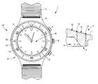
- FIG. 1 is a diagram of a timepiece according to the invention
- FIG. 2 is a top view of a ceramic element before it is inlaid according to the invention.
- FIGS. 3 to 8 are successive steps of the manufacturing method according to the invention.
- FIG. 9 is a flow diagram of the method according to the invention.
- FIGS. 10 and 11 are alternative embodiments of the securing device according to the invention.
- FIG. 1 shows a timepiece, generally referenced 1 , including at least one inlaid element 10 .
- Each inlaid element 10 is intended to form a part that is very resistant to wear, including at least one metallic decoration 13 whose visual quality is improved, particularly in terms of contrast.
- the inlaid element 10 may form either all or part of the external part of timepiece 1 .
- it could form all or part of a case 2 , bracelet 3 , bezel 4 , dial 5 , crystal 6 , push button 7 and/or a crown 8 .
- the explanation of the invention will be given with reference to a ring 10 including inlaid decorations 13 , forming the scale marks of a bezel 4 .
- inlaid elements 10 for a timepiece movement such as, for example, a bridge and/or a plate and/or an oscillating weight.
- inlaid ceramic element 10 includes a body 11 including at least one recess 12 forming the pattern cavity for a decoration 13 .
- FIG. 1 shows that, advantageously according to the invention, each decoration 13 may take any form, such as, for example, a geometrical figure or an alphanumerical character.
- each recess 12 is entirely filled with a galvanic deposition 16 formed by a metallic material. This configuration protects each decoration 13 in body 11 .
- body 11 is made of electrically conductive material such as a cermet.
- a cermet is a material formed by a mixture of ceramic and metal. It may, for example, include TiC, SiN or ZrC to form all or part of body 11 .
- body 11 may also be made of a material which is not electrically conductive.
- decoration 13 further includes at least one electrically conductive layer 15 of substantially 50 nm between body 11 and galvanic deposition 16 .
- Body 11 may then be formed, for example, of a zirconia-based ceramic used for its mechanical properties, polishing ability and, to a lesser extent, for its ability to offer a broad palette of colours.
- body 11 may be formed from an electrically conductive or non-conductive material. Consequently, body 11 is obtainable from a large variety of materials.
- recess 12 preferably has a depth comprised between 80 ⁇ m and 200 ⁇ m.
- each recess 12 has a continuous, at least partially rounded surface, i.e. the inner surface thereof does not include any edges.
- inlaid element 10 further includes a device for fixedly securing said at least one metallic decoration 13 communicating with said at least one recess 12 to improve the securing of said at least one decoration 13 against said element 10 .
- the securing device includes at least one hole 14 through said element 10 which is at least partially filled by said galvanic deposition 16 and, where appropriate, said at least one electrically conductive layer 15 in order to increase the surface of contact with said element.
- the diameter of hole 14 may flare gradually as it gets further away from said at least one recess 12 in order to hold said galvanic deposition 16 and, where appropriate, said at least one electrically conductive layer 15 , against said element 10 .
- the diameter of hole 14 opening into recess 12 is smaller than the rest of hole 14 , decorations 13 can no longer be removed.
- galvanic deposition 16 may also completely fill said at least one hole 14 in order to maximise the surface of contact with body 18 , 18 ′ of the element.
- galvanic deposition 16 may also completely fill said at least one hole 14 in order to maximise the surface of contact with body 18 , 18 ′ of the element.
- body 18 includes at least one recess 12 communicating with at least one hole 14 which opens onto the surface P opposite the surface F intended to receive said at least one recess 12 . It is thus clear that body 18 is hollowed on both sides. Moreover, preferably, galvanic deposition 16 covers shoulder 19 of the end of said at least one hole 14 which is opposite the end communicating with said at least one recess 12 in order to block any movement of said at least one decoration 13 relative to body 18 . It is thus clear that galvanic deposition 16 projects relative to said opposite surface P.
- body 18 ′ includes at least one recess 12 communicating with at least one hole 14 which opens onto a recess 20 in the surface P opposite surface F intended to receive said at least one recess 12 . It is thus clear that body 18 ′ is hollowed on both sides. Moreover, preferably, galvanic deposition 16 covers shoulder 19 of the end of said at least one hole 14 which is opposite the end communicating with said at least one recess 12 in order to block any movement of said at least one decoration 13 relative to body 18 ′. It is thus clear that galvanic deposition 16 is intended to remain only in recess 20 , i.e. not to project relative to said opposite surface P.
- a layer intended to improve the force of adherence of the future decoration 13 onto body 11 .
- a layer for example of substantially 50 nm, may be deposited between galvanic deposition 16 and where appropriate, electrically conductive layer 15 and body 11 , 18 , 18 ′.
- materials may be envisaged, such as, for example, Cr, Cr 2 N, TiN, TiW, Ni, NiP, Cu, Ti or Zr.
- Galvanic deposition 16 and, where appropriate, said at least one electrically conductive layer 15 may also be formed from a wide variety of materials.
- electrically conductive layer 15 is selected for its adherence properties and for its high level of electrical conductivity, which is necessary for electroforming.
- each decoration 13 is mainly obtained via the colour of galvanic deposition 16 . Consequently, the material used for galvanic deposition 16 will preferably be guided by the colour, or more generally, the aesthetic appearance thereof. Therefore, metal galvanic deposition 16 and, incidentally, layer 15 include gold and/or copper and/or silver and/or indium and/or platinum and/or palladium and/or nickel.
- decorations 13 may be formed with the same metal to offer a homogeneous appearance or with several different metals in order, for example, to provide a different colour between two decorations such as one colour for the indices and another for the alphanumerical characters in the case of FIG. 1 .
- decorations 13 in the same material as that surrounding body 11 , 18 , 18 ′.
- decorations 13 of bezel 4 in the same material as case 2 , bracelet 3 , the rest of bezel 4 , dial 5 , push buttons 7 and/or crown 8 .
- the inlaid element 10 may, according to the invention, also provide an optional, substantially transparent layer, in order to protect decorations 13 from ageing.
- This layer may, for example, include silicon nitride to prevent galvanic deposition 16 and, where appropriate, said at least one electrically conductive layer 15 from tarnishing, especially when they are mainly silver-based.
- body 11 may be manufactured from a material other than electrically non-conductive ceramic, as explained above.
- method 21 consists in forming the body 11 , for example, of zirconia.
- the final body 11 of step 22 is preferably obtained by sintering, i.e. from an unfired body 17 preformed via an injection process.
- the body 11 visible in FIG. 4 has its final dimensions.
- method 21 includes a second step 23 , for etching at least one blind recess 12 in one surface F of ceramic body 11 , with recesses 12 forming the pattern cavity for future decorations 13 as visible in FIGS. 2 and 5 .
- each recess 12 has a depth P comprised between 80 ⁇ m and 200 ⁇ m.
- each recess 12 has a continuous, at least partially rounded surface in order to facilitate implementation of the electroforming step 26 explained below.
- Step 23 is preferably obtained by destructive radiation using a laser in order to obtain highly precise etchings.
- method 21 continues with a third step 24 for etching at least one hole 14 communicating with each recess 12 so as to form a securing device.
- a third step 24 for etching at least one hole 14 communicating with each recess 12 so as to form a securing device.
- Step 24 is preferably obtained by destructive radiation using a laser in order to obtain highly precise etchings.
- each hole 14 passes through body 11 of element 10 so that it can be at least partially filled during step 26 by the metallic material 16 and, where appropriate, during steps 25 and 25 ′ by said at least one electrically conductive layer 15 , in order to increase the surface of contact with said element.
- the electrolyte can thus flow “in front of” and “behind” recess 12 , i.e. it can be deposited in each recess 12 and in each hole 14 at any time in electroforming step 26 .
- each hole 14 flares gradually as it gets further away from said at least one recess 12 , in order to block the future metallic material 16 and, where appropriate, said at least one electrically conductive layer 15 against element 10 .
- each hole 14 can thus have a diameter substantially equal to 100 ⁇ m at the bottom of recess 12 and finish with a diameter substantially equal to 120 ⁇ m or more on the surface P opposite body 11 .
- step 24 is achieved by orienting the laser beam from the opposite surface P so as to form said at least one hole 14 immediately in a conical manner, i.e. in which the largest diameter is at the join with the opposite surface P.
- step 24 continues with step 25 ′ of method 21 consisting in depositing at least one electrically conductive layer 15 of substantially 50 nm over the whole of surface F comprising said at least one recess 12 and said at least one hole 14 .
- Step 25 ′ may be achieved by a wet method, such as, for example, electroless plating, or by a dry method, such as, for example, physical vapour deposition.
- step 26 After step 25 ′, method 21 continues with step 26 .
- this layer 15 may, for example, be made of gold and/or copper and/or silver and/or indium and/or platinum and/or palladium and/or nickel.
- step 24 is followed by step 25 of method 21 consisting in depositing an intermediate layer as explained above.
- the intermediate layer is then preferably made using a dry method, such as, for example, physical vapour deposition.
- step 25 method 21 continues either with step 25 ′ of the first embodiment before passing to step 26 , or immediately with step 26 .
- step 24 is immediately followed by step 26 .
- This embodiment concerns the first variant which preferably uses an electrically conductive ceramic as the material for body 11 .
- Step 26 consists of the galvanic deposition of a metallic material 16 from surface F of body 11 and, where appropriate, conductive layer 15 , so as to completely fill each recess 12 and at least partially fill each hole 14 , as seen in FIG. 7 . Further, as explained in the two alternatives of the securing device of FIGS. 10 and 11 , in step 26 , the metallic deposition 16 can completely fill said at least one hole 14 . Finally, in this same step 26 , metal deposition 16 covers shoulder 19 of the end of said at least one hole 14 , which is opposite the end communicating with said at least one recess 12 so as to block any movement of at least one decoration 13 relative to body 18 , 18 ′.
- electrolyte renewal is forced by agitation in recesses 12 , holes 14 and, where appropriate, recesses 20 , i.e. by implementing a forced displacement of the galvanic bath fluids, so as to prevent any problems in filling recesses 12 , holes 14 and, where appropriate, recesses 20 .
- the metallic material deposited in step 26 includes gold and/or copper and/or silver and/or indium and/or platinum and/or palladium and/or nickel.
- step 27 method 21 ends with the removal of any deposition 16 , and where appropriate, 15 from surface F of body 11 , 18 , 18 ′, so that deposition is only left in each recess 12 and holes 14 as seen in FIGS. 8 , 10 and 11 .
- Inlaid element 10 is thus finished and simply requires assembly in a final part.
- This step 27 can be obtained by a usual surfacing method such as grinding or lapping to remove any surplus material, followed by polishing.
- Method 21 according to the invention may also have an optional final step for depositing a substantially transparent layer so as to protect decorations 13 from ageing.
- This layer may, for example, include silicon nitride to prevent metallic material 16 and, where appropriate, said at least one electrically conductive layer 15 from tarnishing, especially when they are mainly formed from a silver base.
- inlaid element 10 is in no way limited to a timepiece 1 .
- inlaid element 10 could, by way of example, be applied to a piece of jewellery or even to tableware.
- step 23 could also be switched with the forming of holes 14 in step 24 without losing the advantages of the invention. It is also possible to envisage substituting laser etching in step 23 and/or step 24 with another type of etching if the precision and reject rate thereof are acceptable.
- step 25 or step 25 ′ is not limited to electroless plating or physical vapour deposition, but may alternatively be achieved, for example, by chemical vapour deposition, atomic layer deposition or ionic bombardment.
Landscapes
- Chemical & Material Sciences (AREA)
- Physics & Mathematics (AREA)
- General Physics & Mathematics (AREA)
- Engineering & Computer Science (AREA)
- Chemical Kinetics & Catalysis (AREA)
- Electrochemistry (AREA)
- Materials Engineering (AREA)
- Metallurgy (AREA)
- Organic Chemistry (AREA)
- Adornments (AREA)
- Electroplating Methods And Accessories (AREA)
- Physical Vapour Deposition (AREA)
Applications Claiming Priority (3)
| Application Number | Priority Date | Filing Date | Title |
|---|---|---|---|
| EP12155635.1 | 2012-02-15 | ||
| EP12155635 | 2012-02-15 | ||
| EP12155635.1A EP2628607B1 (fr) | 2012-02-15 | 2012-02-15 | Dispositif d'ancrage d'une incrustation métallique |
Publications (2)
| Publication Number | Publication Date |
|---|---|
| US20130208577A1 US20130208577A1 (en) | 2013-08-15 |
| US9150978B2 true US9150978B2 (en) | 2015-10-06 |
Family
ID=45655866
Family Applications (1)
| Application Number | Title | Priority Date | Filing Date |
|---|---|---|---|
| US13/764,961 Active 2033-12-26 US9150978B2 (en) | 2012-02-15 | 2013-02-12 | Device for fixedly securing a metallic inlay |
Country Status (6)
| Country | Link |
|---|---|
| US (1) | US9150978B2 (fr) |
| EP (1) | EP2628607B1 (fr) |
| JP (1) | JP2013167628A (fr) |
| CN (2) | CN108749459A (fr) |
| IN (1) | IN2013CH00544A (fr) |
| RU (1) | RU2620941C2 (fr) |
Cited By (3)
| Publication number | Priority date | Publication date | Assignee | Title |
|---|---|---|---|---|
| USD820693S1 (en) * | 2017-03-17 | 2018-06-19 | Citizen Watch Co., Ltd. | Watch |
| USD823139S1 (en) * | 2017-01-27 | 2018-07-17 | Citizen Watch Co., Ltd. | Watch |
| US20200269356A1 (en) * | 2019-02-25 | 2020-08-27 | Comadur Sa | Method for producing a multi-decoration and/or multicoloured horological component having a ceramic structure |
Families Citing this family (37)
| Publication number | Priority date | Publication date | Assignee | Title |
|---|---|---|---|---|
| US9753436B2 (en) | 2013-06-11 | 2017-09-05 | Apple Inc. | Rotary input mechanism for an electronic device |
| KR102035445B1 (ko) | 2013-08-09 | 2019-10-22 | 애플 인크. | 전자 시계 |
| CH708654A2 (fr) * | 2013-10-01 | 2015-04-15 | Rado Montres Sa | Procédé de fabrication d'un élément céramique incrusté d'une pièce d'horlogerie et pièces d'horlogerie incluant de tels éléments. |
| WO2015122885A1 (fr) | 2014-02-12 | 2015-08-20 | Bodhi Technology Ventures Llc | Rejet de mauvaises rotations d'entrées rotatives de dispositifs électroniques |
| CN106462106B (zh) * | 2014-04-04 | 2022-06-28 | 劳力士有限公司 | 制备带有复合材料制成的插入件的计时器部件的方法以及相关的计时器部件和计时器 |
| US10190891B1 (en) | 2014-07-16 | 2019-01-29 | Apple Inc. | Optical encoder for detecting rotational and axial movement |
| KR102414569B1 (ko) | 2014-09-02 | 2022-06-29 | 애플 인크. | 웨어러블 전자 디바이스 |
| JP6515185B2 (ja) | 2015-03-05 | 2019-05-15 | アップル インコーポレイテッドApple Inc. | 方向依存光学特性を有する光学エンコーダを有する時計、手首装着型電子デバイス及びウェラブル電子デバイス |
| KR101993073B1 (ko) | 2015-03-08 | 2019-06-25 | 애플 인크. | 회전가능 및 병진가능한 입력 메커니즘을 위한 압축성 밀봉부 |
| US10018966B2 (en) | 2015-04-24 | 2018-07-10 | Apple Inc. | Cover member for an input mechanism of an electronic device |
| EP3141969A1 (fr) * | 2015-09-10 | 2017-03-15 | Omega SA | Élément d'habillage à circuit de communication intégré |
| EP3185085B1 (fr) * | 2015-12-21 | 2019-05-08 | The Swatch Group Research and Development Ltd. | Applique de cadran d'une pièce d'horlogerie |
| US9891651B2 (en) | 2016-02-27 | 2018-02-13 | Apple Inc. | Rotatable input mechanism having adjustable output |
| AU201614768S (en) * | 2016-03-01 | 2016-10-12 | Omega Sa Omega Ag Omega Ltd | Bezel for a watch |
| US10551798B1 (en) | 2016-05-17 | 2020-02-04 | Apple Inc. | Rotatable crown for an electronic device |
| US10061399B2 (en) | 2016-07-15 | 2018-08-28 | Apple Inc. | Capacitive gap sensor ring for an input device |
| US10019097B2 (en) | 2016-07-25 | 2018-07-10 | Apple Inc. | Force-detecting input structure |
| JP1599796S (fr) * | 2016-11-02 | 2018-03-19 | ||
| CH713250B1 (fr) * | 2016-12-16 | 2021-01-29 | Rubattel Et Weyermann S A | Procédé de fabrication d'un élément d'habillage, notamment d'un cadran, d'horlogerie ou de bijouterie, en matériau non conducteur et comportant des décors gravés métallisés et/ou colorés. |
| US10664074B2 (en) | 2017-06-19 | 2020-05-26 | Apple Inc. | Contact-sensitive crown for an electronic watch |
| US10962935B1 (en) | 2017-07-18 | 2021-03-30 | Apple Inc. | Tri-axis force sensor |
| US11360440B2 (en) | 2018-06-25 | 2022-06-14 | Apple Inc. | Crown for an electronic watch |
| EP3587626B1 (fr) * | 2018-06-28 | 2023-02-22 | Comadur S.A. | Pièce décorative réalisée par incrustation |
| EP3587625A1 (fr) * | 2018-06-28 | 2020-01-01 | Comadur S.A. | Procédé de fabrication de pièces décoratives |
| US11561515B2 (en) | 2018-08-02 | 2023-01-24 | Apple Inc. | Crown for an electronic watch |
| CN209560398U (zh) | 2018-08-24 | 2019-10-29 | 苹果公司 | 电子表 |
| US11181863B2 (en) | 2018-08-24 | 2021-11-23 | Apple Inc. | Conductive cap for watch crown |
| CN209625187U (zh) | 2018-08-30 | 2019-11-12 | 苹果公司 | 电子手表和电子设备 |
| US11194298B2 (en) | 2018-08-30 | 2021-12-07 | Apple Inc. | Crown assembly for an electronic watch |
| US11194299B1 (en) | 2019-02-12 | 2021-12-07 | Apple Inc. | Variable frictional feedback device for a digital crown of an electronic watch |
| EP3786722A1 (fr) * | 2019-08-27 | 2021-03-03 | Comadur S.A. | Procede de decoration d'une piece mecanique |
| EP3819718A1 (fr) | 2019-11-08 | 2021-05-12 | Rolex Sa | Revêtement coloré conçu pour composants de montre |
| EP3832398A1 (fr) * | 2019-12-04 | 2021-06-09 | Comadur S.A. | Systeme de lunette tournante comprenant une lunette tournante en ceramique |
| US11550268B2 (en) | 2020-06-02 | 2023-01-10 | Apple Inc. | Switch module for electronic crown assembly |
| EP3951512B1 (fr) * | 2020-08-04 | 2023-03-01 | Comadur S.A. | Procede de fabrication d'une piece comprenant au moins un motif metallise en trois dimensions |
| EP4009116A1 (fr) * | 2020-12-03 | 2022-06-08 | Comadur S.A. | Article en cermet et/ou ceramique et son procédé de fabrication |
| CN115503383A (zh) * | 2022-09-29 | 2022-12-23 | 黄向文 | 一种外表面具有掐丝图文结构的物品及其加工方法 |
Citations (10)
| Publication number | Priority date | Publication date | Assignee | Title |
|---|---|---|---|---|
| US5270612A (en) * | 1992-02-21 | 1993-12-14 | Zenith Electronics Corporation | Inlaid support for an FTM mask support structure |
| US20020097279A1 (en) | 2000-11-14 | 2002-07-25 | Masaaki Mimura | Mark forming method and product using the same method |
| US20040032797A1 (en) * | 2000-11-01 | 2004-02-19 | Masaaki Sato | Timepiece dial and production method therefor |
| US20040233795A1 (en) * | 2001-09-21 | 2004-11-25 | Citizen Watch Co., Ltd | Timepiece external part and method of manufacturing the part |
| US20050126917A1 (en) * | 2003-12-16 | 2005-06-16 | Seiko Epson Corporation | Decorative component, method of manufacturing a decorative component, timepiece, and decorated component |
| US20050185518A1 (en) * | 2004-02-02 | 2005-08-25 | Seiko Epson Corporation | Decorative article, method of manufacturing same, and timepiece |
| EP2138323A1 (fr) | 2008-06-23 | 2009-12-30 | The Swatch Group Research and Development Ltd. | Pièce décorative réalisée par incrustation |
| US20100214882A1 (en) * | 2004-09-22 | 2010-08-26 | Asulab S.A. | Multi-stage enamelled dial |
| US20110236580A1 (en) * | 2008-11-28 | 2011-09-29 | The Swatch Group Research And Development Ltd. | Three dimensional decoration method |
| EP2380864A1 (fr) | 2010-04-23 | 2011-10-26 | Omega SA | Elément céramique incrusté d'au moins un décor métallique |
Family Cites Families (10)
| Publication number | Priority date | Publication date | Assignee | Title |
|---|---|---|---|---|
| US3798730A (en) * | 1968-12-10 | 1974-03-26 | V Morf | Process for the attachment of hour signs on time piece dials |
| SU690430A1 (ru) * | 1977-09-14 | 1979-10-05 | Петродворцовый Ордена Трудового Красного Знамени Часовой Завод | Способ изготовлени накладных занков дл часовых циферблатов |
| JPS60147672A (ja) * | 1984-01-13 | 1985-08-03 | Citizen Watch Co Ltd | 時計用文字板 |
| JPH05139099A (ja) * | 1991-11-20 | 1993-06-08 | Kazuo Saeki | 象嵌模様を有する装飾品 |
| DE69917744T2 (de) * | 1999-03-05 | 2005-07-07 | Eta Sa Manufacture Horlogère Suisse | Zifferblatt für Uhren mit Brillanten, Auflegestücken oder anderen eingesetzen Elementen und Verfahren zur Befestigung dieser Elemente an einem solchen Zifferblatt |
| JP3584908B2 (ja) * | 2000-10-18 | 2004-11-04 | セイコーエプソン株式会社 | 装飾板、および、その製造方法、ならびに、この装飾板を利用する装飾品および時計 |
| RU2194427C2 (ru) * | 2001-01-31 | 2002-12-20 | Тихонков Александр Константинович | Способ изготовления ювелирных или декоративных изделий |
| EP1548524B1 (fr) * | 2003-12-23 | 2007-08-22 | Rolex S.A. | Elément en céramique pour boîte de montre et procédé de fabrication de cet élément |
| EP2104005A1 (fr) * | 2008-03-20 | 2009-09-23 | Nivarox-FAR S.A. | Balancier composite et son procédé de fabrication |
| JP2010183953A (ja) * | 2009-02-10 | 2010-08-26 | Casio Computer Co Ltd | 装飾装置及び装飾装置の製造方法 |
-
2012
- 2012-02-15 EP EP12155635.1A patent/EP2628607B1/fr active Active
-
2013
- 2013-02-08 CN CN201810612134.7A patent/CN108749459A/zh active Pending
- 2013-02-08 IN IN544CH2013 patent/IN2013CH00544A/en unknown
- 2013-02-08 CN CN2013100506786A patent/CN103253067A/zh active Pending
- 2013-02-12 US US13/764,961 patent/US9150978B2/en active Active
- 2013-02-14 RU RU2013106520A patent/RU2620941C2/ru active
- 2013-02-15 JP JP2013027497A patent/JP2013167628A/ja active Pending
Patent Citations (12)
| Publication number | Priority date | Publication date | Assignee | Title |
|---|---|---|---|---|
| US5270612A (en) * | 1992-02-21 | 1993-12-14 | Zenith Electronics Corporation | Inlaid support for an FTM mask support structure |
| US20040032797A1 (en) * | 2000-11-01 | 2004-02-19 | Masaaki Sato | Timepiece dial and production method therefor |
| US20020097279A1 (en) | 2000-11-14 | 2002-07-25 | Masaaki Mimura | Mark forming method and product using the same method |
| US20040233795A1 (en) * | 2001-09-21 | 2004-11-25 | Citizen Watch Co., Ltd | Timepiece external part and method of manufacturing the part |
| US20050126917A1 (en) * | 2003-12-16 | 2005-06-16 | Seiko Epson Corporation | Decorative component, method of manufacturing a decorative component, timepiece, and decorated component |
| US20050185518A1 (en) * | 2004-02-02 | 2005-08-25 | Seiko Epson Corporation | Decorative article, method of manufacturing same, and timepiece |
| US20100214882A1 (en) * | 2004-09-22 | 2010-08-26 | Asulab S.A. | Multi-stage enamelled dial |
| EP2138323A1 (fr) | 2008-06-23 | 2009-12-30 | The Swatch Group Research and Development Ltd. | Pièce décorative réalisée par incrustation |
| US20110103199A1 (en) | 2008-06-23 | 2011-05-05 | Omega S.A. | Decorative piece made by inlay |
| US20110236580A1 (en) * | 2008-11-28 | 2011-09-29 | The Swatch Group Research And Development Ltd. | Three dimensional decoration method |
| EP2380864A1 (fr) | 2010-04-23 | 2011-10-26 | Omega SA | Elément céramique incrusté d'au moins un décor métallique |
| US20110259753A1 (en) | 2010-04-23 | 2011-10-27 | Omega Sa | Ceramic element inlaid with at least one metallic decoration |
Non-Patent Citations (1)
| Title |
|---|
| European Search Report issued Jul. 10, 2012, in European Patent Application No. 12155635.1, filed Feb. 15, 2012 (with English Translation ). |
Cited By (4)
| Publication number | Priority date | Publication date | Assignee | Title |
|---|---|---|---|---|
| USD823139S1 (en) * | 2017-01-27 | 2018-07-17 | Citizen Watch Co., Ltd. | Watch |
| USD820693S1 (en) * | 2017-03-17 | 2018-06-19 | Citizen Watch Co., Ltd. | Watch |
| US20200269356A1 (en) * | 2019-02-25 | 2020-08-27 | Comadur Sa | Method for producing a multi-decoration and/or multicoloured horological component having a ceramic structure |
| US11654515B2 (en) * | 2019-02-25 | 2023-05-23 | Comadur S.A. | Method for producing a multi-decoration and/or multicoloured horological component having a ceramic structure |
Also Published As
| Publication number | Publication date |
|---|---|
| EP2628607B1 (fr) | 2016-08-03 |
| RU2013106520A (ru) | 2014-08-20 |
| CN108749459A (zh) | 2018-11-06 |
| US20130208577A1 (en) | 2013-08-15 |
| EP2628607A1 (fr) | 2013-08-21 |
| RU2620941C2 (ru) | 2017-05-30 |
| IN2013CH00544A (fr) | 2015-08-07 |
| JP2013167628A (ja) | 2013-08-29 |
| CN103253067A (zh) | 2013-08-21 |
Similar Documents
| Publication | Publication Date | Title |
|---|---|---|
| US9150978B2 (en) | Device for fixedly securing a metallic inlay | |
| US9453287B2 (en) | Ceramic element inlaid with at least one metallic decoration | |
| US9588495B2 (en) | Method for manufacturing a selectively conductive ceramic coated with metallic material | |
| KR101631764B1 (ko) | 적어도 하나의 세라믹 장식과 함께 인레이된 세라믹 엘리먼트 | |
| KR20210138546A (ko) | 세라믹 구조체를 가지는 멀티-장식 및/또는 다색의 시계 구성요소를 제조하는 방법 | |
| US11687039B2 (en) | Method for assembling at least two elements | |
| US11027574B2 (en) | Process for the production of a timepiece provided with a raised external element | |
| KR102435084B1 (ko) | 장식 부품을 제조하기 위한 방법 | |
| JP6980933B2 (ja) | 象嵌することによって製造される装飾部品 | |
| JP2021096229A (ja) | 機械部品を装飾するための方法 | |
| CN117724197A (zh) | 包括衍射光栅的外装部件的制造方法 |
Legal Events
| Date | Code | Title | Description |
|---|---|---|---|
| AS | Assignment |
Owner name: OMEGA S.A., SWITZERLAND Free format text: ASSIGNMENT OF ASSIGNORS INTEREST;ASSIGNORS:NETUSCHILL, ALEXANDRE;FROELICHER, THOMAS;REEL/FRAME:029797/0142 Effective date: 20130109 |
|
| STCF | Information on status: patent grant |
Free format text: PATENTED CASE |
|
| MAFP | Maintenance fee payment |
Free format text: PAYMENT OF MAINTENANCE FEE, 4TH YEAR, LARGE ENTITY (ORIGINAL EVENT CODE: M1551); ENTITY STATUS OF PATENT OWNER: LARGE ENTITY Year of fee payment: 4 |
|
| MAFP | Maintenance fee payment |
Free format text: PAYMENT OF MAINTENANCE FEE, 8TH YEAR, LARGE ENTITY (ORIGINAL EVENT CODE: M1552); ENTITY STATUS OF PATENT OWNER: LARGE ENTITY Year of fee payment: 8 |