US9146567B2 - Current control device - Google Patents
Current control device Download PDFInfo
- Publication number
- US9146567B2 US9146567B2 US13/985,627 US201213985627A US9146567B2 US 9146567 B2 US9146567 B2 US 9146567B2 US 201213985627 A US201213985627 A US 201213985627A US 9146567 B2 US9146567 B2 US 9146567B2
- Authority
- US
- United States
- Prior art keywords
- current
- duty
- current control
- semiconductor element
- command value
- Prior art date
- Legal status (The legal status is an assumption and is not a legal conclusion. Google has not performed a legal analysis and makes no representation as to the accuracy of the status listed.)
- Active, expires
Links
Images


Classifications
-
- G—PHYSICS
- G05—CONTROLLING; REGULATING
- G05F—SYSTEMS FOR REGULATING ELECTRIC OR MAGNETIC VARIABLES
- G05F1/00—Automatic systems in which deviations of an electric quantity from one or more predetermined values are detected at the output of the system and fed back to a device within the system to restore the detected quantity to its predetermined value or values, i.e. retroactive systems
- G05F1/10—Regulating voltage or current
-
- H—ELECTRICITY
- H02—GENERATION; CONVERSION OR DISTRIBUTION OF ELECTRIC POWER
- H02M—APPARATUS FOR CONVERSION BETWEEN AC AND AC, BETWEEN AC AND DC, OR BETWEEN DC AND DC, AND FOR USE WITH MAINS OR SIMILAR POWER SUPPLY SYSTEMS; CONVERSION OF DC OR AC INPUT POWER INTO SURGE OUTPUT POWER; CONTROL OR REGULATION THEREOF
- H02M7/00—Conversion of ac power input into dc power output; Conversion of dc power input into ac power output
- H02M7/42—Conversion of dc power input into ac power output without possibility of reversal
- H02M7/44—Conversion of dc power input into ac power output without possibility of reversal by static converters
- H02M7/48—Conversion of dc power input into ac power output without possibility of reversal by static converters using discharge tubes with control electrode or semiconductor devices with control electrode
- H02M7/53—Conversion of dc power input into ac power output without possibility of reversal by static converters using discharge tubes with control electrode or semiconductor devices with control electrode using devices of a triode or transistor type requiring continuous application of a control signal
- H02M7/537—Conversion of dc power input into ac power output without possibility of reversal by static converters using discharge tubes with control electrode or semiconductor devices with control electrode using devices of a triode or transistor type requiring continuous application of a control signal using semiconductor devices only, e.g. single switched pulse inverters
- H02M7/538—Conversion of dc power input into ac power output without possibility of reversal by static converters using discharge tubes with control electrode or semiconductor devices with control electrode using devices of a triode or transistor type requiring continuous application of a control signal using semiconductor devices only, e.g. single switched pulse inverters in a push-pull configuration
- H02M7/53803—Conversion of dc power input into ac power output without possibility of reversal by static converters using discharge tubes with control electrode or semiconductor devices with control electrode using devices of a triode or transistor type requiring continuous application of a control signal using semiconductor devices only, e.g. single switched pulse inverters in a push-pull configuration with automatic control of output voltage or current
-
- H02P29/021—
-
- H02P29/022—
-
- H02P29/023—
-
- H—ELECTRICITY
- H02—GENERATION; CONVERSION OR DISTRIBUTION OF ELECTRIC POWER
- H02P—CONTROL OR REGULATION OF ELECTRIC MOTORS, ELECTRIC GENERATORS OR DYNAMO-ELECTRIC CONVERTERS; CONTROLLING TRANSFORMERS, REACTORS OR CHOKE COILS
- H02P29/00—Arrangements for regulating or controlling electric motors, appropriate for both AC and DC motors
- H02P29/02—Providing protection against overload without automatic interruption of supply
- H02P29/024—Detecting a fault condition, e.g. short circuit, locked rotor, open circuit or loss of load
- H02P29/0241—Detecting a fault condition, e.g. short circuit, locked rotor, open circuit or loss of load the fault being an overvoltage
-
- H—ELECTRICITY
- H02—GENERATION; CONVERSION OR DISTRIBUTION OF ELECTRIC POWER
- H02P—CONTROL OR REGULATION OF ELECTRIC MOTORS, ELECTRIC GENERATORS OR DYNAMO-ELECTRIC CONVERTERS; CONTROLLING TRANSFORMERS, REACTORS OR CHOKE COILS
- H02P29/00—Arrangements for regulating or controlling electric motors, appropriate for both AC and DC motors
- H02P29/02—Providing protection against overload without automatic interruption of supply
- H02P29/024—Detecting a fault condition, e.g. short circuit, locked rotor, open circuit or loss of load
- H02P29/0243—Detecting a fault condition, e.g. short circuit, locked rotor, open circuit or loss of load the fault being a broken phase
-
- H—ELECTRICITY
- H02—GENERATION; CONVERSION OR DISTRIBUTION OF ELECTRIC POWER
- H02P—CONTROL OR REGULATION OF ELECTRIC MOTORS, ELECTRIC GENERATORS OR DYNAMO-ELECTRIC CONVERTERS; CONTROLLING TRANSFORMERS, REACTORS OR CHOKE COILS
- H02P29/00—Arrangements for regulating or controlling electric motors, appropriate for both AC and DC motors
- H02P29/02—Providing protection against overload without automatic interruption of supply
- H02P29/032—Preventing damage to the motor, e.g. setting individual current limits for different drive conditions
-
- H—ELECTRICITY
- H01—ELECTRIC ELEMENTS
- H01F—MAGNETS; INDUCTANCES; TRANSFORMERS; SELECTION OF MATERIALS FOR THEIR MAGNETIC PROPERTIES
- H01F7/00—Magnets
- H01F7/06—Electromagnets; Actuators including electromagnets
- H01F7/08—Electromagnets; Actuators including electromagnets with armatures
- H01F7/18—Circuit arrangements for obtaining desired operating characteristics, e.g. for slow operation, for sequential energisation of windings, for high-speed energisation of windings
- H01F2007/1888—Circuit arrangements for obtaining desired operating characteristics, e.g. for slow operation, for sequential energisation of windings, for high-speed energisation of windings using pulse width modulation
-
- H—ELECTRICITY
- H02—GENERATION; CONVERSION OR DISTRIBUTION OF ELECTRIC POWER
- H02M—APPARATUS FOR CONVERSION BETWEEN AC AND AC, BETWEEN AC AND DC, OR BETWEEN DC AND DC, AND FOR USE WITH MAINS OR SIMILAR POWER SUPPLY SYSTEMS; CONVERSION OF DC OR AC INPUT POWER INTO SURGE OUTPUT POWER; CONTROL OR REGULATION THEREOF
- H02M1/00—Details of apparatus for conversion
- H02M1/32—Means for protecting converters other than automatic disconnection
Definitions
- the present invention relates to a current control device, and particularly relates to a current control device suitable for failure diagnosis of a current detection circuit.
- an electric actuator such as a motor and a solenoid in order to convert an electrical signal into mechanical movement or hydraulic pressure with the increase in electronic control of various controlled objects.
- an electric actuator is used for control that involves human life such as control in a motor vehicle, the electric actuator is required to have high reliability.
- a current control device is implemented using a current control semiconductor element which has, on the same semiconductor element, a transistor which drives load, a current detection circuit which detects current of the load, and a compensator which calculates an on-duty of the transistor from a current command value and a current value output from the current detection circuit, and a microcontroller which sends the current command value to the current control semiconductor element to thereby achieve downsizing and price reduction of the current control device.
- the present invention provides a current control device including: a current control semiconductor element including, on a same semiconductor chip, a transistor for driving load, current detection circuit for detecting current of the load, a compensator for calculating an on-duty of the transistor from a current command value and a current value output from the current detection circuit, and a PWM timer for generating a pulse turning on the transistor on the basis of the on-duty; and a microcontroller for sending the current command value to the current control semiconductor element, wherein the microcontroller receives a current value output from the current detection circuit and an on-duty output from the compensator from the current control semiconductor element, and detects failure of the current control semiconductor element on the basis of the current value and the on-duty both received from the current control semiconductor element.
- This configuration makes it possible to perform widely applicable failure detection.
- the microcontroller detects failure of the current control semiconductor element when the current value received from the current control semiconductor element does not agree with a current command value, or when the on-duty received from the current control semiconductor element does not agree with an expected value of the on-duty.
- the microcontroller sends zero as an on-duty command value to the current control semiconductor element after detecting failure of the current control semiconductor element, and the current control semiconductor element performs off control of the transistor in accordance with the on-duty command value received from the microcontroller.
- the current control semiconductor element includes a selector for selecting either an on-duty output from the compensator or the on-duty command value received from the microcontroller, and the selector selects the on-duty command value received from the microcontroller on the basis of information on a valid bit output from the microcontroller and performs off control of the transistor in accordance with the on-duty command value.
- the current control semiconductor element includes a zero detector for detecting that the on-duty command value received from the microcontroller is zero, and the zero detector causes output of the PWM timer to become zero to perform off control of the transistor.
- the microcontroller sends an on-duty command value to the current control semiconductor element after detecting failure of the current control semiconductor element, and the current control semiconductor element performs on and off control of the transistor in accordance with the on-duty command value received from the microcontroller.
- the current control semiconductor element includes a selector for selecting either an on-duty output from the compensator or the on-duty command value received from the microcontroller, and the selector selects the on-duty command value received from the microcontroller on the basis of information on a valid bit output from the microcontroller and performs on and off control of the transistor in accordance with the on-duty command value.
- the current control semiconductor element includes, in addition to the PWM timer for generating a pulse turning on the transistor on the basis of an on-duty output from the compensator, a second PWM timer for generating a pulse turning on the transistor on the basis of the on-duty command value received from the microcontroller, and a selector for selecting either a pulse output from the PWM timer or a pulse output from the second PWM timer, and the selector selects the pulse output from the second PWM timer on the basis of information on a valid bit output from the microcontroller and performs on and off control of the transistor in accordance with the pulse.
- FIG. 1 is a block diagram illustrating the configuration of a solenoid control system using a current control device according to a first embodiment of the present invention.
- FIG. 2 is an explanatory diagram of a data format of an on-duty command value register used in the current control device according to the first embodiment of the present invention.
- FIG. 3 is a timing chart illustrating the operation of a fail-stop function in the current control device according to the first embodiment of the present invention.
- FIG. 4 is a timing chart illustrating the operation of a fail-operative function in the current control device according to the first embodiment of the present invention.
- FIG. 5 is a block diagram illustrating the configuration of a solenoid control system using a current control device according to a second embodiment of the present invention.
- FIG. 6 is a block diagram illustrating the configuration of a solenoid control system using a current control device according to a third embodiment of the present invention.
- FIG. 7 is a block diagram illustrating the configuration of an automatic transmission control unit using the current control semiconductor element according to each of the embodiments of the present invention.
- FIG. 8 is a block diagram illustrating the configuration of a brake control unit using the current control semiconductor element according to each of the embodiments of the present invention.
- FIG. 9 is a block diagram illustrating the configuration of a brushless motor control unit using the current control semiconductor element according to each of the embodiments of the present invention.
- FIGS. 1 to 4 the configuration and the operation of a current control device according to a first embodiment of the present invention will be described with reference to FIGS. 1 to 4 .
- FIG. 1 is a block diagram illustrating the configuration of the solenoid control system using the current control device according to the first embodiment of the present invention.
- the current control device of the present embodiment includes a current control semiconductor element 1 and a microcontroller 6 .
- the microcontroller 6 inputs voltage of a battery 3 , temperature of a solenoid 2 detected by a solenoid temperature sensor 17 , and values from other various sensors which are not shown, calculates a current command value for the solenoid 2 from these values, and sends the calculated value to the current control semiconductor element 1 via an interface circuit 10 .
- the current control semiconductor element 1 controls current to be delivered from the battery 3 to the solenoid 2 on the basis of the current command value sent from the microcontroller 6 .
- the current control semiconductor element 1 is connected to the solenoid 2 and the battery 3 which supplies voltage to the solenoid 2 , and turns on and off voltage to be applied to the solenoid 2 by pulse width modulation (PWM) to thereby drive current flowing into the solenoid 2 .
- PWM pulse width modulation
- the microcontroller 6 reads out a current monitor value I_m and an on-duty monitor value Duty_m from the current control semiconductor element 1 via the interface circuit 10 to thereby detect failure of the current control semiconductor element 1 .
- a method of the failure detection will be described later with reference to FIG. 3 .
- the microcontroller 6 sends an on-duty command value Duty_t to the current control semiconductor element 1 via the interface circuit 10 to thereby achieve a fail-stop function or a fail-operative function. Details of this operation will be described later with reference to FIGS. 3 and 4 .
- the current control semiconductor element 1 is provided with a high-side MOSFET 4 , a low-side MOSFET 5 , a current detection circuit 7 , a compensator 8 , a difference calculator 9 , the interface (IF) circuit 10 , a selector 11 , a PWM timer 12 , a current command value register 13 , a current monitor value register 14 , an on-duty command value register 15 , and an on-duty monitor value register 16 .
- IF interface
- the high-side MOSFET 4 is a switch between the solenoid 2 and the battery 3 .
- the high-side MOSFET 4 is turned on when a gate signal thereof is at a high level, and turned off when the gate signal is at a low level.
- the high-side MOSFET 4 is in an on state, current flowing in the solenoid 2 increases.
- the high-side MOSFET 4 is in an off state, current flowing in the solenoid 2 decreases.
- the high-side MOSFET 4 is in an on state, the low-side MOFET 5 is in an off state.
- the low-side MOFET 5 is used as a path through which current which has flowed into the solenoid 2 flows back when the high-side MOSFET 4 is in an off state. When the high-side MOSFET 4 is in an off state, the low-side MOFET 5 is in an on state.
- the current detection circuit 7 outputs the current monitor value I_m which is an average value of current flowing in the solenoid 2 .
- the current detection circuit 7 is connected in series to the solenoid 2 and measures all current flowing in the solenoid 2 .
- the current detection circuit 7 may be connected in parallel to the high-side MOSFET 4 or the low-side MOFET 5 and measure shunt current from the current flowing in the solenoid 2 .
- the current monitor value I_m output from the current detection circuit 7 is input to the compensator 8 and the current monitor value register 14 .
- the compensator 8 calculates an optimal on-duty value Duty — 0 for causing the current in the solenoid 2 to follow the current command value I_t.
- the calculated on-duty value Duty — 0 is input to the selector 11 and the on-duty monitor value register 16 .
- the selector 11 selects either the on-duty value Duty — 0 input from the compensator 8 or the on-duty command value Duty_t input from the on-duty command value register 15 , and then outputs the selected value as a duty.
- FIG. 2 is an explanatory diagram of the data format of the on-duty command value register used in the current control device according to the first embodiment of the present invention.
- the on-duty command value register 15 is a 16-bit register. Contents of respective fields of the duty command value register 15 are as follows.
- any other number of bits than 16 can be selected for the on-duty command value register 15 depending on required accuracy.
- the selector 11 shown in FIG. 1 selects the Duty_t when the valid bit V is one or selects the Duty — 0 when the valid bit V is zero, and outputs the selected value as a duty.
- the PWM timer 12 generates each of a pulse that turns on the high-side MOSFET 4 and a pulse that turns on the low-side MOFET 5 according to the Duty from the selector 11 . Normally, the PWM timer 12 generates each of the pulse that turns on the high-side MOSFET 4 and the pulse that turns on the low-side MOFET 5 on the basis of the on-duty value Duty — 0 from the compensator 8 .
- the IF circuit 10 provides an interface function for sending and receiving values retained in the current command value register 13 , the current monitor value register 14 , the on-duty command value register 15 , and the on-duty monitor value register 16 between the microcontroller 6 and these registers via the IF circuit 10 .
- FIG. 3 is a timing chart illustrating the operation of a fail-stop function in the current control device according to the first embodiment of the present invention.
- FIG. 4 is a timing chart illustrating the operation of a fail-operative function in the current control device according to the first embodiment of the present invention.
- a horizontal axis represents time.
- a vertical axis of (A) represents a command and data transferred over the interface circuit 10 to be fetched into the microcontroller 6 via the interface circuit 10 .
- a vertical axis of (B) represents current flowing in the solenoid 2 .
- a vertical axis of (C) represents the current monitor value I_m.
- a vertical axis of (D) represents the on-duty monitor value Duty_m.
- a vertical axis of (E) represents a duty value Duty.
- the current control device is in normal operation at times t0 to t3, and in abnormal operation at a time t4 or later.
- the microcontroller 6 outputs a read command of the current monitor value register 14 on the interface circuit 10 as shown in (A) in FIG. 3 to thereby read out a current monitor value I_m ((C) in FIG. 3 ) output from the current detection circuit 7 of the current control semiconductor element 1 .
- the microcontroller 6 outputs a read command of the on-duty monitor value register 14 on the interface circuit 10 as shown in (A) in FIG. 3 to thereby read out an on-duty monitor value Duty_m ((D) in FIG. 3 ) output from the compensator 8 of the current control semiconductor element 1 .
- the microcontroller 6 performs failure detection by comparing the read-out current monitor value I_m and the read-out on-duty monitor value Duty_m with respective expected values.
- an expected value of the current monitor value I_m is the current command value I_t
- an expected value Duty_e of the on duty monitor value Duty_m is calculated by the following formula (1).
- Duty — e I — t ⁇ R/Vb (1)
- Vb denotes a voltage of the battery 3
- R denotes a resistance value of the solenoid 2 .
- the resistance value R can be obtained by compensating the temperature characteristics in a solenoid resistance value at a normal temperature by a solenoid temperature input from the solenoid temperature sensor 17 .
- the current monitor value I_m read out at the time t0 and the on-duty monitor value Duty_m read out at the time t1 agree with the respective expected values. Therefore, it is determined that the current control semiconductor element 1 is in normal operation.
- the failure detection is continuously performed also at the time t2 and the time t3 by comparing a current monitor value I_m and an on-duty monitor value Duty_m with respective expected values in the same manner as above. Although not shown in FIG. 3 , the same failure detection is regularly performed thereafter.
- the compensator 8 increases the Duty — 0 by ⁇ D in order to cause the current monitor value I_m to approach the current command value I_t, that is, to increase the lowered current monitor value I_m.
- the compensator 8 performs feedback control so that the current monitor value I_m agrees with the current command value I_t. Therefore, a dangerous situation is caused by the gradually increased current by the compensator 8 . In view of this, when such failure of the current detection circuit occurs, the operation of the current control device is stopped (a fail-stop function).
- the microcontroller 6 performs determination of agreement/disagreement at a normal time where the current command value from the microcontroller 6 is maintained substantially constant. This is because of that, during a transition period where the current command value changes, “disagreement” determination is highly likely to be made constantly due to a difference between a command value and a measured value. Further, a determination criterion between agreement and disagreement should be previously determined such that “agreement” determination is made when a difference between the command value and the measured value is, for example, within ⁇ 1%, and “disagreement” determination is made when the difference between the command value and the measured value is, for example, larger than ⁇ 1%.
- the output of the PWM timer 12 is fixed to zero at a time t8, and the current in the solenoid is thereby stopped.
- the present embodiment makes it possible to achieve the fail-stop function of the small and low-cost current control device which is implemented with the current control semiconductor element 1 and the microcontroller 6 .
- FIG. 4 a horizontal axis represents time.
- Vertical axes of (A) to (E) in FIG. 4 are the same as those of (A) to (E) in FIG. 3 .
- the current control device is in normal operation at times t0 to t3, and in abnormal operation at a time t4 or later.
- the same failure detection as described with reference to FIG. 3 is performed at the time t0 to the time t4, and it is determined that the current control semiconductor element 1 is in normal operation. Although not shown in FIG. 4 , the same failure detection is regularly performed thereafter.
- control can be performed until the vehicle is pulled over on the shoulder of a road.
- a case where a solenoid current control device is used as an actuator of an electric braking device, or a case where a motor current control device is used as an actuator of an electric power steering device falls under the above case.
- the operation of the current control device is continued (a fail-operative function).
- a current monitor value I_m of the current detection circuit 7 the current monitor value I_m being read out at the time t5 after the occurrence of the above failure ((C) in FIG. 4 ) does not agree with an expected value thereof.
- the microcontroller 6 detects the failure. Since a failure location cannot be identified at this point, the operation may be continued.
- the Duty_e is a positive value other than zero.
- the on-duty of the output pulse of the PWM timer 12 becomes Duty_e ((E) in FIG. 4 ), and, at the time t7, the solenoid current returns to I_t, namely, to a normal state ((C) in FIG. 4 ).
- the microcontroller 6 reads out a current monitor value I_m ((C) and (A) in FIG. 4 ), and compares the thus read-out current monitor value I_m with an expected value thereof. Then, the microcontroller 6 confirms that the current control device has actually returned to the normal state on the basis of the written contents in the on-duty command value register 15 .
- the present invention makes it possible to achieve the fail-operative function of the small and low-cost current control device which is implemented with the current control semiconductor element 1 and the microcontroller 6 .
- failure of the current control device is detected on the basis of the on-duty which is always calculated for controlling current and the current value output from the current detection circuit in the present embodiment, it is possible to achieve failure detection means of the current control device that is widely applicable and does not depend on the type of a sensor to be used.
- the microcontroller reads out the on-duty and the current value output from the current detection circuit from the current control semiconductor element to thereby perform failure diagnosis. Accordingly, it is possible to perform failure detection of the current control device which is implemented with the current control semiconductor element and the microcontroller.
- the microcontroller calculates and sends the on-duty command value on behalf of the failed current control semiconductor, thereby making it possible to achieve the fail-stop function or the fail-operative function of the current control device which is implemented with the current control semiconductor element and the microcontroller.
- FIG. 5 is a block diagram illustrating the configuration of the solenoid control system using the current control device according to the second embodiment of the present invention.
- the same reference sings as those in FIG. 1 refer to the same elements.
- a current control semiconductor element 1 ′ of the present embodiment is provided with a zero detector 20 , an AND gate 21 , and an AND gate 22 in addition to the configuration of the current control semiconductor element 1 of the first embodiment described with reference to FIG. 1 .
- the AND gate 21 and the AND gate 22 fix the output of the PWM timer 12 to zero.
- the above configuration makes it possible to reliably execute a fail-safe function by writing zero to the on-duty command value register 15 to thereby turn off the high-side MOSFET 4 and the low-side MOSFET 5 even when failure of the selector 11 or the PWM timer 12 occurs.
- failure of the current control device is detected on the basis of the on-duty which is always calculated for controlling current and the current value output from the current detection circuit in the present embodiment, it is possible to achieve failure detection means of the current control device that is widely applicable and does not depend on the type of a sensor to be used.
- the microcontroller reads out the on-duty and the current value output from the current detection circuit from the current control semiconductor element to thereby perform failure diagnosis. Accordingly, it is possible to perform failure detection of the current control device which is implemented with the current control semiconductor element and the microcontroller.
- the fail-stop function of the current control device can be reliably achieved.
- FIG. 6 is a block diagram illustrating the configuration of the solenoid control system using the current control device according to the third embodiment of the present invention.
- the same reference sings as those in FIG. 1 refer to the same elements.
- the PWM timer 12 of the current control semiconductor element 1 of the first embodiment described with reference to FIG. 1 is duplicated into a PWM timer m 12 A as a main and a PWM timer b 12 B for backup. Further, the outputs of these two PWM timers 12 A and 12 B are selected by using a selector 11 A and a selector 11 B.
- the above configuration makes it possible to reliably execute a fail-safe function and a fail-operative function by writing a value to the on-duty command value register 15 to thereby output an on-duty pulse corresponding to the written value to the high-side MOSFET 4 and the low-side MOSFET 5 even when failure of the PWM timer m 12 A occurs.
- failure of the current control device is detected on the basis of the on-duty which is always calculated for controlling current and the current value output from the current detection circuit in the present embodiment, it is possible to achieve failure detection means of the current control device that is widely applicable and does not depend on the type of a sensor to be used.
- the microcontroller reads out the on-duty and the current value output from the current detection circuit from the current control semiconductor element to thereby perform failure diagnosis. Accordingly, it is possible to perform failure detection of the current control device which is implemented with the current control semiconductor element and the microcontroller.
- the fail-stop function or the fail-operative function of the current control device can be reliably achieved.
- FIG. 7 is a block diagram illustrating the configuration of the automatic transmission control unit using the current control semiconductor element according to each of the embodiments of the present invention.
- the same reference sings as those in FIG. 1 refer to the same elements.
- An automatic transmission control unit ATCU includes the microcontroller 6 shown in FIG. 1 , and a plurality of current control semiconductor elements 1 a to 1 e which correspond to the current control semiconductor element 1 .
- the microcontroller 6 inputs sensor values from an engine rotation speed sensor 52 , a shift lever position sensor 53 , and an accelerator pedal position sensor 54 , calculates an optimal transmission gear ratio from the input sensor values, calculates, for realizing the optimal transmission gear ratio, hydraulic pressure command values of a plurality of clutches (not shown) provided in a transmission 51 and current command values of solenoids 20 a to 20 e , the current command values corresponding to the respective hydraulic pressure command values, and outputs the calculated current command values Ia* to Ie* to the respective current control semiconductor elements 1 a to 1 e.
- the microcontroller 6 is capable of improving reliability of the automatic transmission control unit ATCU by achieving reliable failure detection of the current control semiconductor elements 1 a to 1 e , the fail-safe function, and the fail-operative function.
- the microcontroller 6 inputs the sensor values from three sensors including the engine rotation speed sensor 52 , the shift lever position sensor 53 , and the accelerator pedal position sensor 54 .
- the number or the type of sensors from which sensor values are input may be changed according to a transmission control method.
- the microcontroller 6 inputs the sensor values directly from the sensors in FIG. 7
- the sensor values may be input via another microcontroller or an integrated circuit (IC).
- IC integrated circuit
- the number of clutches and the number of solenoid current control devices corresponding to the number of clutches may be changed according to a transmission mechanism.
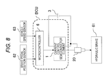
- FIG. 8 the same reference sings as those in FIG. 1 refer to the same elements.
- FIG. 8 is a block diagram illustrating the configuration of the brake control unit using the current control semiconductor element according to each of the embodiments of the present invention.
- the same reference sings as those in FIG. 1 refer to the same elements.
- a brake control unit BCU includes the microcontroller 6 and the current control semiconductor element 1 both of which are shown in FIG. 1 .
- the microcontroller 6 inputs sensor values from a brake pedal position sensor 63 and a vehicle speed sensor 64 , calculates an optimal braking force from the input sensor values, calculates, for realizing the optimal braking force, a hydraulic pressure command value of a hydraulic brake 61 and a current command value of a solenoid 20 , the current command value corresponding to the hydraulic pressure command value, and outputs the calculated current command value I* to the current control semiconductor element 1 .
- the microcontroller 6 is capable of improving reliability of the brake control unit BCU by achieving reliable failure detection of the current control semiconductor element 1 , the fail-safe function, and the fail-operative function.
- the microcontroller 6 inputs the sensor values from two sensors including the brake pedal position sensor 63 and the vehicle speed sensor 64 .
- the number or the type of sensors from which sensor values are input may be changed according to a transmission control method.
- the microcontroller 6 inputs the sensor values directly from the sensors in FIG. 8 , the sensor values may be input via another microcontroller or an IC.
- FIG. 9 is a block diagram illustrating the configuration of the brushless motor control unit using the current control semiconductor element according to each of the embodiments of the present invention.
- the same reference sings as those in FIG. 1 refer to the same elements.
- a brushless motor control unit MCU includes the microcontroller 6 and the current control semiconductor element 1 both of which are shown in FIG. 1 .
- the microcontroller 6 calculates a target rotation speed of a motor and a three-phase current command values with respect to three phase coils Cu, Cv and Cw of the motor 71 for realizing torque, and outputs the calculated current command values Iu*, Iv* and Iw* to respective current control semiconductor elements 1 a to 1 c.
- the microcontroller 6 is capable of improving reliability of the brushless motor control unit MCU by achieving reliable failure detection of the current control semiconductor elements 1 a to 1 c , the fail-safe function, and the fail-operative function.
Landscapes
- Engineering & Computer Science (AREA)
- Power Engineering (AREA)
- Physics & Mathematics (AREA)
- Electromagnetism (AREA)
- General Physics & Mathematics (AREA)
- Radar, Positioning & Navigation (AREA)
- Automation & Control Theory (AREA)
- Control Of Electric Motors In General (AREA)
- Electronic Switches (AREA)
- Magnetically Actuated Valves (AREA)
Applications Claiming Priority (3)
| Application Number | Priority Date | Filing Date | Title |
|---|---|---|---|
| JP2011-049823 | 2011-03-08 | ||
| JP2011049823A JP5537470B2 (ja) | 2011-03-08 | 2011-03-08 | 電流制御装置 |
| PCT/JP2012/054161 WO2012121007A1 (ja) | 2011-03-08 | 2012-02-21 | 電流制御装置 |
Publications (2)
| Publication Number | Publication Date |
|---|---|
| US20130320948A1 US20130320948A1 (en) | 2013-12-05 |
| US9146567B2 true US9146567B2 (en) | 2015-09-29 |
Family
ID=46797976
Family Applications (1)
| Application Number | Title | Priority Date | Filing Date |
|---|---|---|---|
| US13/985,627 Active 2032-09-27 US9146567B2 (en) | 2011-03-08 | 2012-02-21 | Current control device |
Country Status (5)
| Country | Link |
|---|---|
| US (1) | US9146567B2 (ja) |
| JP (1) | JP5537470B2 (ja) |
| CN (1) | CN103348588B (ja) |
| DE (1) | DE112012001148B4 (ja) |
| WO (1) | WO2012121007A1 (ja) |
Families Citing this family (8)
| Publication number | Priority date | Publication date | Assignee | Title |
|---|---|---|---|---|
| DE102013007287A1 (de) * | 2013-01-11 | 2014-07-17 | Assa Abloy Sicherheitstechnik Gmbh | Zugangbestimmende Vorrichtung in einem Gebäude |
| JP6194466B2 (ja) * | 2013-04-11 | 2017-09-13 | パナソニックIpマネジメント株式会社 | モータ駆動装置 |
| WO2017014216A1 (ja) * | 2015-07-21 | 2017-01-26 | アイシン・エィ・ダブリュ株式会社 | 制御装置 |
| CN105443840B (zh) * | 2016-01-08 | 2017-10-10 | 浙江大学 | 一种电磁阀智能控制系统及其方法 |
| CN109958815B (zh) * | 2017-12-22 | 2020-10-27 | 圣邦微电子(北京)股份有限公司 | 一种具有电磁柱塞运动检测电路的电磁驱动器 |
| CN109713864A (zh) | 2019-03-08 | 2019-05-03 | 关伟伟 | 一种电流主控电动机 |
| CN110098781A (zh) * | 2019-04-19 | 2019-08-06 | 深圳市雷赛智能控制股份有限公司 | 电机驱动器及自动化设备 |
| CN111198590B (zh) * | 2019-12-26 | 2022-02-18 | 苏州浪潮智能科技有限公司 | 一种服务器供电低温控制的方法及装置 |
Citations (8)
| Publication number | Priority date | Publication date | Assignee | Title |
|---|---|---|---|---|
| JPH03213464A (ja) | 1990-01-17 | 1991-09-18 | Koyo Seiko Co Ltd | 電動式パワーステアリング装置 |
| JPH08205388A (ja) | 1995-01-27 | 1996-08-09 | Aisin Seiki Co Ltd | 直流モータの異常検出装置 |
| US20050093505A1 (en) | 2003-11-04 | 2005-05-05 | Denso Corporation | Motor driving system |
| JP2008199851A (ja) | 2007-02-15 | 2008-08-28 | Denso Corp | Dcモータ接地異常判定装置 |
| JP2008306838A (ja) | 2007-06-07 | 2008-12-18 | Panasonic Corp | ブラシレスdcモータ駆動装置とそれを搭載した換気送風装置 |
| US7825642B1 (en) * | 2007-05-09 | 2010-11-02 | Zilker Labs, Inc. | Control system optimization via independent parameter adjustment |
| US20130082675A1 (en) * | 2011-09-23 | 2013-04-04 | Infineon Technologies Ag | Digital Switching Converter Control |
| US20130147449A1 (en) * | 2006-08-25 | 2013-06-13 | Lawson Labs, Inc. | Bi-polar bi-directional energy balancing power-conversion engine |
Family Cites Families (2)
| Publication number | Priority date | Publication date | Assignee | Title |
|---|---|---|---|---|
| JPH0787698B2 (ja) * | 1989-03-13 | 1995-09-20 | 株式会社日立製作所 | 電力変換器の制御装置及びエレベーター装置 |
| JP3521842B2 (ja) | 2000-04-13 | 2004-04-26 | 株式会社デンソー | モータ駆動装置 |
-
2011
- 2011-03-08 JP JP2011049823A patent/JP5537470B2/ja active Active
-
2012
- 2012-02-21 DE DE112012001148.1T patent/DE112012001148B4/de active Active
- 2012-02-21 WO PCT/JP2012/054161 patent/WO2012121007A1/ja active Application Filing
- 2012-02-21 CN CN201280006960.8A patent/CN103348588B/zh active Active
- 2012-02-21 US US13/985,627 patent/US9146567B2/en active Active
Patent Citations (9)
| Publication number | Priority date | Publication date | Assignee | Title |
|---|---|---|---|---|
| JPH03213464A (ja) | 1990-01-17 | 1991-09-18 | Koyo Seiko Co Ltd | 電動式パワーステアリング装置 |
| JPH08205388A (ja) | 1995-01-27 | 1996-08-09 | Aisin Seiki Co Ltd | 直流モータの異常検出装置 |
| US20050093505A1 (en) | 2003-11-04 | 2005-05-05 | Denso Corporation | Motor driving system |
| JP2005143153A (ja) | 2003-11-04 | 2005-06-02 | Denso Corp | モータ駆動装置 |
| US20130147449A1 (en) * | 2006-08-25 | 2013-06-13 | Lawson Labs, Inc. | Bi-polar bi-directional energy balancing power-conversion engine |
| JP2008199851A (ja) | 2007-02-15 | 2008-08-28 | Denso Corp | Dcモータ接地異常判定装置 |
| US7825642B1 (en) * | 2007-05-09 | 2010-11-02 | Zilker Labs, Inc. | Control system optimization via independent parameter adjustment |
| JP2008306838A (ja) | 2007-06-07 | 2008-12-18 | Panasonic Corp | ブラシレスdcモータ駆動装置とそれを搭載した換気送風装置 |
| US20130082675A1 (en) * | 2011-09-23 | 2013-04-04 | Infineon Technologies Ag | Digital Switching Converter Control |
Non-Patent Citations (1)
| Title |
|---|
| International Search Report dated May 22, 2012 with English translation (5 pages). |
Also Published As
| Publication number | Publication date |
|---|---|
| JP2012186966A (ja) | 2012-09-27 |
| CN103348588A (zh) | 2013-10-09 |
| US20130320948A1 (en) | 2013-12-05 |
| JP5537470B2 (ja) | 2014-07-02 |
| DE112012001148T5 (de) | 2014-01-02 |
| CN103348588B (zh) | 2016-02-24 |
| WO2012121007A1 (ja) | 2012-09-13 |
| DE112012001148B4 (de) | 2021-07-22 |
Similar Documents
| Publication | Publication Date | Title |
|---|---|---|
| US9146567B2 (en) | Current control device | |
| US8738232B2 (en) | Electronic control apparatus | |
| US10562563B2 (en) | Device and method for controlling electric motor | |
| US10097129B2 (en) | Drive controller and drive control method for electric motor | |
| US8901863B2 (en) | Motor control device | |
| US8766589B2 (en) | Motor control unit and vehicle steering system | |
| CN112351933B (zh) | 具有冗余配置的控制单元的机动车辆转向系统 | |
| US20150236626A1 (en) | Brushless motor control device and brushless motor system | |
| JP5117925B2 (ja) | ハイサイドドライバ | |
| CN110417314B (zh) | 马达控制装置及电动助力转向装置 | |
| US20200140005A1 (en) | Motor control device | |
| US20150365024A1 (en) | Motor Control System | |
| JP2015087118A (ja) | 異常診断装置及びそれを用いたシフトバイワイヤ装置 | |
| JP2010115082A (ja) | モータ制御装置 | |
| CN107110348B (zh) | 车辆用自动变速器的电子控制装置 | |
| JP5724906B2 (ja) | 電子制御装置、異常検出方法 | |
| JP2009131069A (ja) | モータ制御装置 | |
| US8204658B2 (en) | Automatic transmission control apparatus | |
| CN108802611B (zh) | 异常诊断装置和异常诊断方法 | |
| KR20170065430A (ko) | 복합 센싱 장치 | |
| JP7186161B2 (ja) | 電動パワーステアリング制御装置および制御方法 | |
| JP2010137860A (ja) | 車両制御装置 | |
| KR101163253B1 (ko) | 차속 센서와 엔진속 센서를 이용하여 단락을 감지하는 방법및 전동식 조향장치 | |
| CN116746051A (zh) | 电机控制装置及其方法 | |
| KR20210019638A (ko) | 브레이크 고장 감지 방법 |
Legal Events
| Date | Code | Title | Description |
|---|---|---|---|
| AS | Assignment |
Owner name: HITACHI AUTOMOTIVE SYSTEMS, LTD., JAPAN Free format text: ASSIGNMENT OF ASSIGNORS INTEREST;ASSIGNORS:HIROTSU, TEPPEI;ISHIDA, RYOSUKE;KANEKAWA, NOBUYASU;SIGNING DATES FROM 20130529 TO 20130530;REEL/FRAME:031082/0444 |
|
| STCF | Information on status: patent grant |
Free format text: PATENTED CASE |
|
| MAFP | Maintenance fee payment |
Free format text: PAYMENT OF MAINTENANCE FEE, 4TH YEAR, LARGE ENTITY (ORIGINAL EVENT CODE: M1551); ENTITY STATUS OF PATENT OWNER: LARGE ENTITY Year of fee payment: 4 |
|
| AS | Assignment |
Owner name: HITACHI ASTEMO, LTD., JAPAN Free format text: CHANGE OF NAME;ASSIGNOR:HITACHI AUTOMOTIVE SYSTEMS, LTD.;REEL/FRAME:056299/0447 Effective date: 20210101 |
|
| MAFP | Maintenance fee payment |
Free format text: PAYMENT OF MAINTENANCE FEE, 8TH YEAR, LARGE ENTITY (ORIGINAL EVENT CODE: M1552); ENTITY STATUS OF PATENT OWNER: LARGE ENTITY Year of fee payment: 8 |