US9054027B2 - III-nitride device and method having a gate isolating structure - Google Patents
III-nitride device and method having a gate isolating structure Download PDFInfo
- Publication number
- US9054027B2 US9054027B2 US13/886,429 US201313886429A US9054027B2 US 9054027 B2 US9054027 B2 US 9054027B2 US 201313886429 A US201313886429 A US 201313886429A US 9054027 B2 US9054027 B2 US 9054027B2
- Authority
- US
- United States
- Prior art keywords
- gate
- semiconductor device
- isolating structure
- contiguous
- gan fet
- Prior art date
- Legal status (The legal status is an assumption and is not a legal conclusion. Google has not performed a legal analysis and makes no representation as to the accuracy of the status listed.)
- Active, expires
Links
Images


Classifications
-
- H01L29/2003—
-
- H—ELECTRICITY
- H10—SEMICONDUCTOR DEVICES; ELECTRIC SOLID-STATE DEVICES NOT OTHERWISE PROVIDED FOR
- H10D—INORGANIC ELECTRIC SEMICONDUCTOR DEVICES
- H10D30/00—Field-effect transistors [FET]
- H10D30/01—Manufacture or treatment
- H10D30/015—Manufacture or treatment of FETs having heterojunction interface channels or heterojunction gate electrodes, e.g. HEMT
-
- H01L29/41725—
-
- H01L29/42316—
-
- H01L29/66462—
-
- H01L29/7787—
-
- H—ELECTRICITY
- H10—SEMICONDUCTOR DEVICES; ELECTRIC SOLID-STATE DEVICES NOT OTHERWISE PROVIDED FOR
- H10D—INORGANIC ELECTRIC SEMICONDUCTOR DEVICES
- H10D30/00—Field-effect transistors [FET]
- H10D30/40—FETs having zero-dimensional [0D], one-dimensional [1D] or two-dimensional [2D] charge carrier gas channels
- H10D30/47—FETs having zero-dimensional [0D], one-dimensional [1D] or two-dimensional [2D] charge carrier gas channels having 2D charge carrier gas channels, e.g. nanoribbon FETs or high electron mobility transistors [HEMT]
- H10D30/471—High electron mobility transistors [HEMT] or high hole mobility transistors [HHMT]
- H10D30/475—High electron mobility transistors [HEMT] or high hole mobility transistors [HHMT] having wider bandgap layer formed on top of lower bandgap active layer, e.g. undoped barrier HEMTs such as i-AlGaN/GaN HEMTs
- H10D30/4755—High electron mobility transistors [HEMT] or high hole mobility transistors [HHMT] having wider bandgap layer formed on top of lower bandgap active layer, e.g. undoped barrier HEMTs such as i-AlGaN/GaN HEMTs having wide bandgap charge-carrier supplying layers, e.g. modulation doped HEMTs such as n-AlGaAs/GaAs HEMTs
-
- H—ELECTRICITY
- H10—SEMICONDUCTOR DEVICES; ELECTRIC SOLID-STATE DEVICES NOT OTHERWISE PROVIDED FOR
- H10D—INORGANIC ELECTRIC SEMICONDUCTOR DEVICES
- H10D64/00—Electrodes of devices having potential barriers
- H10D64/20—Electrodes characterised by their shapes, relative sizes or dispositions
- H10D64/23—Electrodes carrying the current to be rectified, amplified, oscillated or switched, e.g. sources, drains, anodes or cathodes
- H10D64/251—Source or drain electrodes for field-effect devices
-
- H—ELECTRICITY
- H10—SEMICONDUCTOR DEVICES; ELECTRIC SOLID-STATE DEVICES NOT OTHERWISE PROVIDED FOR
- H10D—INORGANIC ELECTRIC SEMICONDUCTOR DEVICES
- H10D64/00—Electrodes of devices having potential barriers
- H10D64/20—Electrodes characterised by their shapes, relative sizes or dispositions
- H10D64/27—Electrodes not carrying the current to be rectified, amplified, oscillated or switched, e.g. gates
- H10D64/311—Gate electrodes for field-effect devices
- H10D64/411—Gate electrodes for field-effect devices for FETs
-
- H—ELECTRICITY
- H10—SEMICONDUCTOR DEVICES; ELECTRIC SOLID-STATE DEVICES NOT OTHERWISE PROVIDED FOR
- H10D—INORGANIC ELECTRIC SEMICONDUCTOR DEVICES
- H10D84/00—Integrated devices formed in or on semiconductor substrates that comprise only semiconducting layers, e.g. on Si wafers or on GaAs-on-Si wafers
- H10D84/80—Integrated devices formed in or on semiconductor substrates that comprise only semiconducting layers, e.g. on Si wafers or on GaAs-on-Si wafers characterised by the integration of at least one component covered by groups H10D12/00 or H10D30/00, e.g. integration of IGFETs
- H10D84/82—Integrated devices formed in or on semiconductor substrates that comprise only semiconducting layers, e.g. on Si wafers or on GaAs-on-Si wafers characterised by the integration of at least one component covered by groups H10D12/00 or H10D30/00, e.g. integration of IGFETs of only field-effect components
-
- H—ELECTRICITY
- H10—SEMICONDUCTOR DEVICES; ELECTRIC SOLID-STATE DEVICES NOT OTHERWISE PROVIDED FOR
- H10D—INORGANIC ELECTRIC SEMICONDUCTOR DEVICES
- H10D62/00—Semiconductor bodies, or regions thereof, of devices having potential barriers
- H10D62/80—Semiconductor bodies, or regions thereof, of devices having potential barriers characterised by the materials
- H10D62/85—Semiconductor bodies, or regions thereof, of devices having potential barriers characterised by the materials being Group III-V materials, e.g. GaAs
- H10D62/8503—Nitride Group III-V materials, e.g. AlN or GaN
Definitions
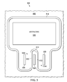
- the gate 512 and the gate isolating structure 514 form a closed loop configuration which surrounds an input/output (I/O) structure 536 and at least one drain contact 520 .
- the I/O structure 536 may be, for example, a probe pad or a bond pad, and may be directly electrically connected to the at least one drain contact 520 or may be electrically coupled to the at least one drain contact 520 through overvoltage protection circuitry.
- At least one source contact 522 is formed outside the closed loop configuration of the gate 512 and the gate isolating structure 514 . The source contact 522 is disposed adjacent to the gate 512 opposite the drain contacts 520 .
- the gate 512 , the source contact 522 and the drain contacts 520 are parts of a GaN FET 524 of the semiconductor device 500 .
- the gate isolating structure 514 electrically isolates the two-dimensional electron gas that is contiguous with the drain contacts 520 from the two-dimensional electron gas that is contiguous with the source contact 522 .
- Disposing the I/O structure 536 inside the closed loop configuration of the gate 512 and the gate isolating structure 514 advantageously allows biasing the drain contacts 520 without undesired leakage current from the I/O structure 536 .
Landscapes
- Junction Field-Effect Transistors (AREA)
- Electrodes Of Semiconductors (AREA)
- Insulated Gate Type Field-Effect Transistor (AREA)
Priority Applications (6)
| Application Number | Priority Date | Filing Date | Title |
|---|---|---|---|
| US13/886,429 US9054027B2 (en) | 2013-05-03 | 2013-05-03 | III-nitride device and method having a gate isolating structure |
| CN201480024829.3A CN105229792B (zh) | 2013-05-03 | 2014-05-05 | Iii族氮化物晶体管布局 |
| PCT/US2014/036788 WO2014179796A1 (en) | 2013-05-03 | 2014-05-05 | Iii-nitride transistor layout |
| JP2016512988A JP2016518723A (ja) | 2013-05-03 | 2014-05-05 | Iii−窒化物トランジスタレイアウト |
| US14/731,744 US9553151B2 (en) | 2013-05-03 | 2015-06-05 | III-nitride device and method having a gate isolating structure |
| JP2019038204A JP2019117935A (ja) | 2013-05-03 | 2019-03-04 | Iii−窒化物トランジスタレイアウト |
Applications Claiming Priority (1)
| Application Number | Priority Date | Filing Date | Title |
|---|---|---|---|
| US13/886,429 US9054027B2 (en) | 2013-05-03 | 2013-05-03 | III-nitride device and method having a gate isolating structure |
Related Child Applications (1)
| Application Number | Title | Priority Date | Filing Date |
|---|---|---|---|
| US14/731,744 Continuation US9553151B2 (en) | 2013-05-03 | 2015-06-05 | III-nitride device and method having a gate isolating structure |
Publications (2)
| Publication Number | Publication Date |
|---|---|
| US20140327011A1 US20140327011A1 (en) | 2014-11-06 |
| US9054027B2 true US9054027B2 (en) | 2015-06-09 |
Family
ID=51840998
Family Applications (2)
| Application Number | Title | Priority Date | Filing Date |
|---|---|---|---|
| US13/886,429 Active 2033-10-03 US9054027B2 (en) | 2013-05-03 | 2013-05-03 | III-nitride device and method having a gate isolating structure |
| US14/731,744 Active US9553151B2 (en) | 2013-05-03 | 2015-06-05 | III-nitride device and method having a gate isolating structure |
Family Applications After (1)
| Application Number | Title | Priority Date | Filing Date |
|---|---|---|---|
| US14/731,744 Active US9553151B2 (en) | 2013-05-03 | 2015-06-05 | III-nitride device and method having a gate isolating structure |
Country Status (4)
| Country | Link |
|---|---|
| US (2) | US9054027B2 (enExample) |
| JP (2) | JP2016518723A (enExample) |
| CN (1) | CN105229792B (enExample) |
| WO (1) | WO2014179796A1 (enExample) |
Cited By (4)
| Publication number | Priority date | Publication date | Assignee | Title |
|---|---|---|---|---|
| US9728600B2 (en) * | 2015-09-11 | 2017-08-08 | Nxp Usa, Inc. | Partially biased isolation in semiconductor devices |
| US9882041B1 (en) | 2016-11-17 | 2018-01-30 | Texas Instruments Incorporated | HEMT having conduction barrier between drain fingertip and source |
| US10381456B2 (en) | 2017-05-04 | 2019-08-13 | Texas Instruments Incorporated | Group IIIA-N HEMT with a tunnel diode in the gate stack |
| US20220139709A1 (en) * | 2020-11-05 | 2022-05-05 | International Business Machines Corporation | Confined gallium nitride epitaxial layers |
Families Citing this family (8)
| Publication number | Priority date | Publication date | Assignee | Title |
|---|---|---|---|---|
| JP2015173237A (ja) * | 2014-03-12 | 2015-10-01 | 株式会社東芝 | 半導体装置 |
| US10811514B2 (en) * | 2018-03-28 | 2020-10-20 | Semiconductor Components Industries, Llc | Electronic device including an enhancement-mode HEMT and a method of using the same |
| DE102020112069B4 (de) * | 2020-02-27 | 2022-03-03 | Taiwan Semiconductor Manufacturing Co. Ltd. | Source-leckstromunterdrückung durch source-umgebende gate-struktur und verfahren zur herstellung der gate-struktur |
| WO2022051173A1 (en) * | 2020-09-01 | 2022-03-10 | Power Integrations, Inc. | A die seal ring including a two dimensional electron gas region |
| US11742390B2 (en) | 2020-10-30 | 2023-08-29 | Texas Instruments Incorporated | Electronic device with gallium nitride transistors and method of making same |
| CN119789461A (zh) * | 2020-12-01 | 2025-04-08 | 深圳市晶相技术有限公司 | 一种功率器件及其应用与制造方法 |
| CN116093165B (zh) * | 2023-04-10 | 2024-07-23 | 深圳市晶扬电子有限公司 | 一种紧凑的低电容型肖特基二极管 |
| FR3155362A1 (fr) | 2023-11-09 | 2025-05-16 | Commissariat A L'energie Atomique Et Aux Energies Alternatives | Dispositif microélectronique à courants de fuite réduits |
Citations (7)
| Publication number | Priority date | Publication date | Assignee | Title |
|---|---|---|---|---|
| US20030102482A1 (en) * | 2001-12-03 | 2003-06-05 | Saxler Adam William | Strain balanced nitride heterojunction transistors and methods of fabricating strain balanced nitride heterojunction transistors |
| US20100102327A1 (en) * | 2008-02-26 | 2010-04-29 | International Rectifier Corporation (El Segundo, Ca) | Semiconductor device and passive component integration in a semiconductor package |
| US20120193677A1 (en) | 2011-02-02 | 2012-08-02 | Transphorm Inc. | III-N Device Structures and Methods |
| US8384129B2 (en) | 2009-06-25 | 2013-02-26 | The United States Of America, As Represented By The Secretary Of The Navy | Transistor with enhanced channel charge inducing material layer and threshold voltage control |
| US8389977B2 (en) | 2009-12-10 | 2013-03-05 | Transphorm Inc. | Reverse side engineered III-nitride devices |
| US20130087803A1 (en) * | 2011-10-06 | 2013-04-11 | Epowersoft, Inc. | Monolithically integrated hemt and schottky diode |
| US8759879B1 (en) * | 2013-05-03 | 2014-06-24 | Texas Instruments Incorporated | RESURF III-nitride HEMTs |
Family Cites Families (17)
| Publication number | Priority date | Publication date | Assignee | Title |
|---|---|---|---|---|
| JPH11121468A (ja) * | 1997-10-08 | 1999-04-30 | Sanyo Electric Co Ltd | 半導体装置 |
| JP2007059595A (ja) * | 2005-08-24 | 2007-03-08 | Toshiba Corp | 窒化物半導体素子 |
| JP5125512B2 (ja) * | 2005-09-30 | 2013-01-23 | 日本電気株式会社 | 電界効果トランジスタ |
| JP2009522812A (ja) * | 2006-01-09 | 2009-06-11 | インターナショナル レクティファイアー コーポレイション | 電界緩和機能を有するiii族窒化物電力半導体 |
| JP4908886B2 (ja) * | 2006-03-23 | 2012-04-04 | 日本電信電話株式会社 | 半導体装置 |
| JP2008112868A (ja) * | 2006-10-30 | 2008-05-15 | Eudyna Devices Inc | 半導体装置およびその製造方法 |
| JP5526470B2 (ja) * | 2007-09-03 | 2014-06-18 | サンケン電気株式会社 | 窒化物系化合物半導体装置 |
| US7985986B2 (en) * | 2008-07-31 | 2011-07-26 | Cree, Inc. | Normally-off semiconductor devices |
| JP5390983B2 (ja) * | 2008-08-08 | 2014-01-15 | 古河電気工業株式会社 | 電界効果トランジスタおよび電界効果トランジスタの製造方法 |
| JP5553997B2 (ja) * | 2009-02-06 | 2014-07-23 | 古河電気工業株式会社 | トランジスタおよびその製造方法 |
| CN102484049B (zh) * | 2009-08-07 | 2015-05-20 | 日本碍子株式会社 | 半导体元件用外延基板、半导体元件用外延基板的制造方法以及半导体元件 |
| JP2011124385A (ja) * | 2009-12-10 | 2011-06-23 | Sanken Electric Co Ltd | 化合物半導体装置及びその製造方法 |
| JP5636867B2 (ja) * | 2010-10-19 | 2014-12-10 | 富士通株式会社 | 半導体装置及び半導体装置の製造方法 |
| US20120153351A1 (en) * | 2010-12-21 | 2012-06-21 | International Rectifier Corporation | Stress modulated group III-V semiconductor device and related method |
| JP5712231B2 (ja) * | 2011-02-15 | 2015-05-07 | シャープ株式会社 | 半導体装置 |
| JP2012238808A (ja) * | 2011-05-13 | 2012-12-06 | Sharp Corp | 電界効果トランジスタ |
| JP2013077638A (ja) * | 2011-09-29 | 2013-04-25 | Sumitomo Electric Ind Ltd | 半導体装置 |
-
2013
- 2013-05-03 US US13/886,429 patent/US9054027B2/en active Active
-
2014
- 2014-05-05 WO PCT/US2014/036788 patent/WO2014179796A1/en not_active Ceased
- 2014-05-05 JP JP2016512988A patent/JP2016518723A/ja active Pending
- 2014-05-05 CN CN201480024829.3A patent/CN105229792B/zh active Active
-
2015
- 2015-06-05 US US14/731,744 patent/US9553151B2/en active Active
-
2019
- 2019-03-04 JP JP2019038204A patent/JP2019117935A/ja active Pending
Patent Citations (7)
| Publication number | Priority date | Publication date | Assignee | Title |
|---|---|---|---|---|
| US20030102482A1 (en) * | 2001-12-03 | 2003-06-05 | Saxler Adam William | Strain balanced nitride heterojunction transistors and methods of fabricating strain balanced nitride heterojunction transistors |
| US20100102327A1 (en) * | 2008-02-26 | 2010-04-29 | International Rectifier Corporation (El Segundo, Ca) | Semiconductor device and passive component integration in a semiconductor package |
| US8384129B2 (en) | 2009-06-25 | 2013-02-26 | The United States Of America, As Represented By The Secretary Of The Navy | Transistor with enhanced channel charge inducing material layer and threshold voltage control |
| US8389977B2 (en) | 2009-12-10 | 2013-03-05 | Transphorm Inc. | Reverse side engineered III-nitride devices |
| US20120193677A1 (en) | 2011-02-02 | 2012-08-02 | Transphorm Inc. | III-N Device Structures and Methods |
| US20130087803A1 (en) * | 2011-10-06 | 2013-04-11 | Epowersoft, Inc. | Monolithically integrated hemt and schottky diode |
| US8759879B1 (en) * | 2013-05-03 | 2014-06-24 | Texas Instruments Incorporated | RESURF III-nitride HEMTs |
Cited By (7)
| Publication number | Priority date | Publication date | Assignee | Title |
|---|---|---|---|---|
| US9728600B2 (en) * | 2015-09-11 | 2017-08-08 | Nxp Usa, Inc. | Partially biased isolation in semiconductor devices |
| US9882041B1 (en) | 2016-11-17 | 2018-01-30 | Texas Instruments Incorporated | HEMT having conduction barrier between drain fingertip and source |
| US10680093B2 (en) | 2016-11-17 | 2020-06-09 | Texas Instruments Incorporated | HEMT having conduction barrier between drain fingertip and source |
| US11177378B2 (en) | 2016-11-17 | 2021-11-16 | Texas Instruments Incorporated | HEMT having conduction barrier between drain fingertip and source |
| US10381456B2 (en) | 2017-05-04 | 2019-08-13 | Texas Instruments Incorporated | Group IIIA-N HEMT with a tunnel diode in the gate stack |
| US10707324B2 (en) | 2017-05-04 | 2020-07-07 | Texas Instruments Incorporated | Group IIIA-N HEMT with a tunnel diode in the gate stack |
| US20220139709A1 (en) * | 2020-11-05 | 2022-05-05 | International Business Machines Corporation | Confined gallium nitride epitaxial layers |
Also Published As
| Publication number | Publication date |
|---|---|
| JP2019117935A (ja) | 2019-07-18 |
| CN105229792A (zh) | 2016-01-06 |
| US9553151B2 (en) | 2017-01-24 |
| WO2014179796A1 (en) | 2014-11-06 |
| US20140327011A1 (en) | 2014-11-06 |
| US20150270357A1 (en) | 2015-09-24 |
| JP2016518723A (ja) | 2016-06-23 |
| CN105229792B (zh) | 2019-10-08 |
Similar Documents
| Publication | Publication Date | Title |
|---|---|---|
| US9553151B2 (en) | III-nitride device and method having a gate isolating structure | |
| US8933461B2 (en) | III-nitride enhancement mode transistors with tunable and high gate-source voltage rating | |
| US8759879B1 (en) | RESURF III-nitride HEMTs | |
| US8502273B2 (en) | Group III-nitride HEMT having a well region formed on the surface of substrate and contacted the buffer layer to increase breakdown voltage and the method for forming the same | |
| US9024357B2 (en) | Method for manufacturing a HEMT transistor and corresponding HEMT transistor | |
| US8809987B2 (en) | Normally-off III-nitride metal-2DEG tunnel junction field-effect transistors | |
| US8969881B2 (en) | Power transistor having segmented gate | |
| US20050173728A1 (en) | Nitride heterojunction transistors having charge-transfer induced energy barriers and methods of fabricating the same | |
| US20080296618A1 (en) | P-GaN/AlGaN/AlN/GaN ENHANCEMENT-MODE FIELD EFFECT TRANSISTOR | |
| Singh et al. | A novel β‐Ga2O3 HEMT with f T of 166 GHz and X‐band P OUT of 2.91 W/mm | |
| CN102769034A (zh) | 常关型高电子迁移率晶体管 | |
| CN102292801A (zh) | 场效应晶体管及其制造方法 | |
| CN108447907A (zh) | 晶体管及其制备方法 | |
| US9653591B2 (en) | Compound semiconductor device having at least one buried semiconductor material region | |
| US9379022B2 (en) | Process for forming driver for normally on III-nitride transistors to get normally-off functionality | |
| Gowrisankar et al. | Compensation dopant-free GaN-on-Si HEMTs with a polarization engineered buffer for RF applications | |
| US12094964B2 (en) | Heterostructure of an electronic circuit having a semiconductor device | |
| Saha | Fabrication and Characterization of Highly Scaled β-Ga2O3 FETs for RF Applications | |
| Du et al. | Design optimization of a high-breakdown-voltage GaN-based vertical HFET with composite current-blocking layer | |
| CN114695507A (zh) | 一种半导体器件的外延结构及其制备方法、半导体器件 | |
| Pei | Advanced gallium nitride based transistors for mm-wave applications |
Legal Events
| Date | Code | Title | Description |
|---|---|---|---|
| AS | Assignment |
Owner name: TEXAS INSTRUMENTS INCORPORATED, TEXAS Free format text: ASSIGNMENT OF ASSIGNORS INTEREST;ASSIGNORS:PENDHARKAR, SAMEER;TIPIRNENI, NAVEEN;JOH, JUNGWOO;SIGNING DATES FROM 20130423 TO 20130502;REEL/FRAME:030344/0365 |
|
| STCF | Information on status: patent grant |
Free format text: PATENTED CASE |
|
| MAFP | Maintenance fee payment |
Free format text: PAYMENT OF MAINTENANCE FEE, 4TH YEAR, LARGE ENTITY (ORIGINAL EVENT CODE: M1551); ENTITY STATUS OF PATENT OWNER: LARGE ENTITY Year of fee payment: 4 |
|
| MAFP | Maintenance fee payment |
Free format text: PAYMENT OF MAINTENANCE FEE, 8TH YEAR, LARGE ENTITY (ORIGINAL EVENT CODE: M1552); ENTITY STATUS OF PATENT OWNER: LARGE ENTITY Year of fee payment: 8 |