US9048957B2 - Signal processing circuit, optical receiver, detector and method for compensating for waveform distortion - Google Patents
Signal processing circuit, optical receiver, detector and method for compensating for waveform distortion Download PDFInfo
- Publication number
- US9048957B2 US9048957B2 US12/822,348 US82234810A US9048957B2 US 9048957 B2 US9048957 B2 US 9048957B2 US 82234810 A US82234810 A US 82234810A US 9048957 B2 US9048957 B2 US 9048957B2
- Authority
- US
- United States
- Prior art keywords
- chromatic dispersion
- electrical signals
- compensator
- signal
- sampling
- Prior art date
- Legal status (The legal status is an assumption and is not a legal conclusion. Google has not performed a legal analysis and makes no representation as to the accuracy of the status listed.)
- Active, expires
Links
Images




Classifications
-
- H—ELECTRICITY
- H04—ELECTRIC COMMUNICATION TECHNIQUE
- H04B—TRANSMISSION
- H04B10/00—Transmission systems employing electromagnetic waves other than radio-waves, e.g. infrared, visible or ultraviolet light, or employing corpuscular radiation, e.g. quantum communication
- H04B10/60—Receivers
- H04B10/61—Coherent receivers
- H04B10/616—Details of the electronic signal processing in coherent optical receivers
- H04B10/6161—Compensation of chromatic dispersion
-
- H—ELECTRICITY
- H04—ELECTRIC COMMUNICATION TECHNIQUE
- H04B—TRANSMISSION
- H04B10/00—Transmission systems employing electromagnetic waves other than radio-waves, e.g. infrared, visible or ultraviolet light, or employing corpuscular radiation, e.g. quantum communication
- H04B10/60—Receivers
-
- H—ELECTRICITY
- H04—ELECTRIC COMMUNICATION TECHNIQUE
- H04B—TRANSMISSION
- H04B10/00—Transmission systems employing electromagnetic waves other than radio-waves, e.g. infrared, visible or ultraviolet light, or employing corpuscular radiation, e.g. quantum communication
- H04B10/60—Receivers
- H04B10/61—Coherent receivers
- H04B10/613—Coherent receivers including phase diversity, e.g., having in-phase and quadrature branches, as in QPSK coherent receivers
-
- H—ELECTRICITY
- H04—ELECTRIC COMMUNICATION TECHNIQUE
- H04B—TRANSMISSION
- H04B10/00—Transmission systems employing electromagnetic waves other than radio-waves, e.g. infrared, visible or ultraviolet light, or employing corpuscular radiation, e.g. quantum communication
- H04B10/60—Receivers
- H04B10/61—Coherent receivers
- H04B10/614—Coherent receivers comprising one or more polarization beam splitters, e.g. polarization multiplexed [PolMux] X-PSK coherent receivers, polarization diversity heterodyne coherent receivers
Definitions
- a certain aspect of the embodiments discussed herein is related to a signal processing circuit, an optical receiver, a detector and a method for compensating for waveform distortion.
- the digital coherent receiver may operate as follows. The receiver extracts information about the optical intensity and phase by coherent receiving, and digitizes the extracted information. Then, the receiver demodulates the digitized information by a digital signal processing circuit.
- the optical communication systems are configured to employ dispersion compensation including chromatic dispersion.
- chromatic dispersion on the transmission path may be compensated for by using the digital signal processing technology.
- the receiver may be configured to estimate the chromatic dispersion on the transmission path and compensate for the estimated chromatic dispersion.
- chromatic dispersion compensation there is known a method for setting the compensation value for dispersion on the basis of the number of corrections by an error correction circuit after demodulation so as to minimize the number of corrections (see Japanese Laid-Open Patent Application Publication Nos. 2002-208892, 2004-236097 and 2008-58610).
- Another method for optimizing the compensation value for chromatic dispersion on the basis of clocks reproduced by an analog clock reproducing circuit see Japanese Laid-Open Patent Application Publication No. 2007-60583
- a signal processing circuit including: a first compensator configured to compensate for waveform distortion corresponding to chromatic dispersion of a received optical signal by using digital electrical signals obtained by sampling analog electrical signals by using a sampling signal, the analog electrical signals being obtained by opto-electric conversion of multiple optical signals that include an intensity of the received optical signal and phase information thereon; and a chromatic dispersion compensation controller configured to control a compensation value for the chromatic dispersion in the first compensation from the digital electrical signals in which the chromatic dispersion has been compensated for on the basis of a detected phase offset between the sampling signal and a modulation frequency of the received optical signal.
- FIG. 1 is a block diagram of an optical receiver
- FIG. 2 is a block diagram of a polarization diversity 90-degree hybrid circuit
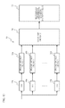
- FIG. 3 is a block diagram of an equalizer and its peripheral circuits
- FIG. 4 is a block diagram of an exemplary configuration of a chromatic dispersion compensator
- FIG. 5 is a block diagram of another configuration of the chromatic dispersion compensator
- FIG. 6 is a block diagram of an exemplary configuration of an adaptive equalizer
- FIG. 7 schematically illustrates sampling phase offset monitor values
- FIG. 8 schematically illustrates the sensitivity of sampling phase offset monitor with respect to residual chromatic dispersion
- FIG. 9 is a flowchart of a process executed in a first embodiment
- FIG. 10 is a block diagram of an equalizer and its peripheral circuits in accordance with a second embodiment
- FIG. 11 is a block diagram of an equalizer and its peripheral circuits in accordance with a third embodiment
- FIG. 12 is a flowchart of a process executed in a third embodiment
- FIG. 13 is a block diagram of a chromatic dispersion compensation controller in accordance with a fourth embodiment
- FIG. 14 is a diagram of a method for detecting maximum/minimum values by a maximum/minimum detector employed in the fourth embodiment
- FIG. 15 is a block diagram of an equalizer and its peripheral circuits in accordance with a fifth embodiment
- FIG. 16 is a flowchart of a process executed in the fifth embodiment
- FIG. 17 is a block diagram of an adaptive equalizer in accordance with a sixth embodiment.
- FIG. 18 is a flowchart of step S 32 depicted in FIG. 16 ;
- FIG. 19 is a block diagram of a receiver in accordance with a seventh embodiment.
- FIG. 20 is a block diagram of a chromatic dispersion detector in accordance with an eighth embodiment.
- a certain aspect of an embodiment takes the following into consideration. It takes a considerable long time to set the optimal compensation value for chromatic dispersion when the method that sets the compensation value on the basis of the number of corrections in forward error correction is used.
- the method that employs the analog clock recovery uses a clock recovery circuit of analog type.
- the receiver handles a considerable large amount of chromatic dispersion because large chromatic dispersion is compensated for by waveform distortion compensation or equalization by digital signal processing. It is thus difficult to employ the analog clock recovery in the digital coherent receiver and set the compensation value in the waveform distortion compensator using the analog clock recovery. It is desired that the digital coherent optical receiver carries out the dispersion compensation appropriately.
- the dispersion compensation may be carried out appropriately.
- FIG. 1 is a block diagram of an optical receiver in accordance with a first embodiment.
- a received optical signal may have a single wavelength that is one of wavelengths obtained by demultiplexing a wavelength-multiplexed optical signal.
- the received optical signal may have a transmission rate of 40 Gbps or 100 Gbps and has been modulated by QPSK (Quadrature Phase shift Keying).
- QPSK Quadrature Phase shift Keying
- the received optical signal is mixed with local light emitted by a local optical oscillator (LO) 42 at a polarization diversity 90-degree hybrid circuit 40 , which extracts real-part signals and imaginary-part signals having orthogonal polarization.
- the real-part signals are referred to as I (in phase) and the imaginary-part signals are referred to as Q (quadrature phase).
- the received optical signal is demodulated by using multiple optical signals that include intensity information and phase information.
- An opto-electric conversion circuit (O/E) 44 converts the multiple analog optical signals of the I and Q of the polarized waves output by the 90-degree hybrid circuit 40 into analog electrical signals.
- Analog-to-digital circuits (ADC) 20 convert the analog electrical signals into digital electrical signals by sampling the analog electrical signals from the O/E conversion circuits 44 at timings synchronized with a sampling signal.
- a sampling clock generator 22 outputs the sampling signal used in A/D conversion by the ADCs 20 .
- the sampling frequency may be twice the modulation frequency of the received optical signal.
- the outputs of the ADCs 20 are applied to a digital signal processing circuit 10 .
- the digital signal processing circuit 10 is equipped with an equalizer 12 , a carrier frequency and phase synchronization circuit 14 , a demodulator 16 and a sampling phase offset detector 28 .
- the equalizer 12 compensates for a waveform distortion caused when the optical signal propagates through the optical transmission path. Waveform distortion that may be compensated for the equalizer 12 may be chromatic dispersion, polarization state dynamics, and polarization mode dispersion.
- the carrier frequency and phase synchronization circuit 14 corrects a phase rotation due to the difference in frequency or phase between the carrier frequency and the local light frequency to thus pull the signals in phase.
- the demodulator 16 identifies the signal to reproduce the digital signal.
- FIG. 2 is a block diagram of the polarization diversity 90-degree hybrid circuit 40 .
- the 90-degree hybrid circuit 40 is equipped with two polarized beam splitters 46 a and 46 b , and 90-degree hybrids 48 a and 48 b .
- the polarized beam splitter 46 a splits the received optical signal into optical signals in two polarization states
- the polarized beam splitter 46 b splits the local light into optical signals in the two polarization states.
- the 90-degree hybrid 48 a extracts the I from the optical signal by using the local light in the corresponding polarization states
- the 90-degree hybrid 48 b extracts the Q from the optical signal by using the local light in the corresponding polarization states.
- the equalizer 12 is equipped with a chromatic dispersion compensator 24 , which functions as a first compensator, an adaptive equalizer 26 , which functions as a second compensator, and a chromatic dispersion compensation controller 30 .
- the chromatic dispersion compensator 24 compensates for chromatic dispersion, which is one of the waveform distortions.
- the chromatic dispersion compensator 24 compensates for waveform distortion that corresponds to chromatic dispersion of the optical signal included in the digital electrical signals.
- the adaptive equalizer 26 compensates for waveform distortion that remains in the output signal of the chromatic dispersion compensator 24 in an adaptive equalization manner. Exemplary remaining waveform distortion may be a variation in the polarized state dynamics, a polarization mode dispersion, and chromatic dispersion that is not compensated for the chromatic dispersion compensator 24 .
- FIG. 4 is a block diagram of an exemplary configuration of the chromatic dispersion compensator 24 .
- the chromatic dispersion compensator 24 is an FIR (finite impulse response) filter, and includes delay elements 50 , FIR coefficients 54 , multipliers 52 and an adder 56 .
- the delay elements 50 delay the input signals by time ⁇ .
- the multipliers 52 multiply the delayed signals by the FIR coefficients C k (n) where k indicates the number of coefficients and is equal to 1-5 in FIG. 4 . An arbitrary number of k may be used.
- the adder 56 adds the signals from the multipliers 52 .
- the chromatic dispersion may be compensated for by setting the FIR coefficients appropriately.
- FIG. 5 is a block diagram of another exemplary configuration of the chromatic dispersion compensator 24 .
- the chromatic dispersion compensator 24 includes a time to frequency domain converting part 60 , a frequency domain chromatic compensation part 62 , and a frequency to time domain converting part 64 .
- the time to frequency domain converting part 60 subjects the input signal to FFT (fast Fourier transform) to convert the input signal into a signal in the frequency domain.
- the frequency domain dispersion compensation part 62 carries out chromatic dispersion compensation in the frequency domain.
- the frequency to time domain region converting part 64 subjects the signal that has been compensated for in terms of chromatic dispersion to inverse FFT to convert the signal into that in the time domain.
- the chromatic dispersion compensation may be carried out in the frequency domain.
- FIG. 6 is a block diagram of an exemplary structure of the adaptive equalizer 26 .
- the adaptive equalizer 26 is equipped with FIR filters 70 a through 70 d , adders 72 a and 72 b , and a weighting factor calculator 74 .
- the adaptive equalizer 26 is supplied with a signal of a horizontally polarized state Ih+jQh and a signal of a vertically polarized state Iv+jQv.
- the signal Ih+jQh is supplied to the FIR filters 70 a and 70 b
- the signal Iv+jQv is supplied to the FIR filters 70 c and 70 d .
- the adder 72 a adds the outputs of the FIR filters 70 a and 70 c , and outputs an added signal Ix+jQx.
- the adder 72 b adds the outputs of the FIR filters 70 b and 70 d , and outputs an added signal Iy+jQy.
- the weighting factor calculator 74 calculates weighting factors of the FIR filters 70 a through 70 d by using the input signals Ih+jQh and Iv+jQv. For example, the weighting factor calculator 74 calculates the weighting factors so as to compensate for waveform distortion of the output signals more effectively (that is, so as to reduce waveform distortion due to residual dispersion). With the above structure, polarization mode dispersion may be compensated for in addition to chromatic dispersion.
- the sampling signal control circuit 29 is equipped with the sampling phase offset detector 28 .
- This detector 28 detects a phase offset between the sampling signal used for the A/D conversion and the analog electrical signal applied to the ADCs 20 , that is, the modulation frequency of the received optical signal.
- the sampling signal control circuit 29 controls the sampling clock generator 22 on the basis of the detected phase offset to control the phase or frequency of the sampling signal. Thus, it is possible to synchronize the received optical signal with the sampling signal.
- the chromatic dispersion compensation controller 30 is equipped with a sensitivity monitor 34 and a part of setting the compensation value for chromatic dispersion.
- the sensitivity monitor 34 monitors the sensitivity of detecting the offset of sampling phase.
- the part 32 of setting the compensation value for chromatic dispersion sets the compensation value for chromatic dispersion in the chromatic dispersion compensator 24 on the basis of the monitored sensitivity. For example, in the example of FIG. 4 , the chromatic dispersion compensator 24 sets the values of the FIR coefficients C k (n).
- FIG. 7 schematically illustrates the sampling phase offset monitor value of the sampling phase offset detector 28 with respect to the sampling phase offset.
- the sampling phase offset (which is the phase offset between the sampling signal and the analog electrical signal applied to the ADCs 20 ) is equal to 1 for a one-cycle offset.
- the sampling phase offset is equal to zero, the phase of the sampling signal is in phase with the analog electrical signals applied to the ADCs 20 .
- the sampling phase offset varies from zero, there is a phase offset between the sampling signal and the analog electrical signals applied to the ADCs 20 .
- a solid line indicates a case where the chromatic dispersion is compensated for in the chromatic dispersion compensator 24
- a broken line indicates a case where there is a residual chromatic dispersion.
- the sampling phase offset detector 28 when the sampling phase offset is zero, the sampling phase does not have any offset and the output value of the sampling phase offset detector 28 , namely, the sampling phase offset monitor value is zero.
- the sensitivity of detection of the sampling phase offset is defined as the absolute value of the slope obtained for phase offsets close to zero ( ⁇ A/ ⁇ B where ⁇ A is the output value and ⁇ B is the phase offset with respect to the origin).
- the output value When the sampling phase has an offset equal to 1 ⁇ 2 UI, the output value returns to zero.
- the waveform is distorted by chromatic dispersion and the sensitivity of detection of phase offset is weakened.
- FIG. 8 schematically illustrates the sensitivity of sampling phase offset monitor with respect to residual chromatic dispersion.
- the residual chromatic dispersion indicates the difference between the compensation value of the chromatic dispersion compensator 24 and the compensation value for chromatic dispersion of the received optical signal.
- the chromatic dispersion compensator 24 compensates for almost all of the chromatic dispersion.
- the residual chromatic dispersion deviates from zero, there is a large residual chromatic dispersion that is not compensated for by the chromatic dispersion compensator 24 .
- FIG. 8 schematically illustrates the sensitivity of sampling phase offset monitor with respect to residual chromatic dispersion.
- the sampling phase offset may be detected by a method described in F. M. Gardner, ABPSK/QPSK Timing-Error Detector for Sampled Receiver, IEEE Trans. Commun. VOL. COM-34, No. 5, May 1986 or T. Tanimura et. Al, Digital clock recovery algorithm for optical coherent receivers operating independent of laser frequency offset, ECOC2008, Mo. 3. D.2.
- FIG. 9 is a flowchart of a process of the first embodiment.
- the sampling signal control circuit 29 steps feeding the sampling phase offset back to the sampling clock generator 22 .
- the phase synchronization loop of the sampling signal is opened (step S 10 ).
- This causes the frequency of the sampling signal to deviate from the modulation frequency of the signals applied to the ADCs 22 .
- a sampling phase offset is swept.
- the part 32 of setting the compensation value for chromatic dispersion sets the compensation value (for example, the FIR coefficients illustrated in FIG. 4 ) to an initial value (step S 12 ).
- the sensitivity monitor 34 monitors the sensitivity of detection of the sampling phase offset (step S 14 ).
- the setting part 32 determines whether the sensitivity is at maximum (step S 16 ). When the answer of step S 16 is NO, the setting part 32 readjusts the compensation value (step S 18 ).
- step S 16 the process returns to step S 14 .
- step S 16 the sampling signal control circuit 29 starts to feed the sampling phase offset back to the sampling clock generator 22 .
- the phase synchronization loop of the sampling signal is closed (step S 20 ).
- the sampling signal is synchronized with the signals applied to the ADCs 22 .
- the adaptive equalizer 26 carries out adaptive equalization (step S 22 ). Thereafter, the carrier frequency and phase synchronization circuit 14 and the demodulator 16 operate.
- the maximum compensation value is set as the initial value used at step S 12 .
- the compensation value for chromatic dispersion is reduced each time step S 18 is carried out.
- the sensitivity is increased.
- the previous step is defined as the maximal sensitivity.
- a predetermined initial value is set at step S 16 .
- the compensation value is alternately increased and decreased from the predetermined initial value so that the compensation value becomes farther away from the predetermined initial value as the number of times that step S 16 is executed becomes larger.
- the chromatic dispersion compensation controller 30 controls the compensation value for chromatic dispersion from the digital electrical signals that haves been subjected to the compensation for chromatic dispersion by the chromatic dispersion compensator 24 on the basis of the phase offset between the sampling signal and the modulation frequency of the received optical signal detected by the sampling phase offset detector 28 . It is thus possible to appropriately compensate for the waveform dispersion by controlling the compensation value for the chromatic dispersion on the basis of the detected phase offset.
- the chromatic dispersion compensation controller 30 controls the compensation value for chromatic dispersion so that the detected phase offset increases. For example, as step S 16 in FIG. 9 , the compensation value is controlled so as to maximize the sensitivity of detection of the sampling phase offset. Thus, as illustrated in FIG. 8 , it is possible to suppress the residual chromatic dispersion of the chromatic dispersion compensator 24 .
- the chromatic dispersion is compensated for by the chromatic dispersion compensator 24
- the residual waveform distortion in the chromatic dispersion compensator 24 is compensated for by the adaptive equalization implemented by the adaptive equalizer 26 .
- the adaptive equalizer 26 has a reduced adaptive dispersion range. It is thus desired to reduce the residual dispersion in the chromatic dispersion compensator 24 .
- the residual dispersion may increase if the estimate differs from the actual waveform dispersion.
- the waveform dispersion is controlled on the basis of the number of corrections by the error correction circuit after demodulation, the number of corrections is calculated, and thereafter, the compensation value is controlled. Thus, it takes much time to control chromatic dispersion.
- the compensation value in the chromatic dispersion compensator 24 is appropriately determined on the basis of the sensitivity of detection of sampling phase offset. It is thus possible to reduce the residual dispersion in the chromatic dispersion compensator 24 . As a result, it is possible to reduce the circuit scale of the adaptive equalizer 26 . Further, the compensation value may be controlled accurately, as compared to the way of estimation from the type and distance of the optical transmission path. As discussed in Documents 1 through 3, high-speed control may be realized because the first embodiment does not have synchronization and demodulation of the sampling clock and the modulation frequency on the contrary to the control of the chromatic dispersion based on the number of corrections.
- step S 10 in FIG. 9 the sampling signal control circuit 29 stops controlling the phase or frequency of the sampling signal when the chromatic dispersion compensator 24 controls the compensation value for chromatic dispersion.
- the phase of the sampling signal is swept, and as illustrated in FIG. 7 , the sensitivity of detection of the sampling phase offset may be monitored.
- a second embodiment has an exemplary configuration in which the compensation for chromatic dispersion is controlled by the maximum or minimum value of the sampling phase offset detected by the sampling phase offset detector 37 .
- FIG. 10 is a block diagram of the equalizer 12 and its peripheral circuits in the second embodiment.
- the chromatic dispersion compensation controller 30 includes the part 32 of setting the compensation value for chromatic dispersion, a sampling phase offset detector 37 , and a maximum/minimum detector 38 .
- the sampling phase offset detector 37 detects the offset of the sampling phase as in the case of the sampling phase offset detector 28 .
- the maximum/minimum detector 38 detects the maximum value and the minimum value of the sampling phase offset monitor value with respect to the sampling phase offset.
- the setting part 32 may determine whether the sensitivity is maximal by determining whether the currently detected sampling phase offset is maximal or minimal at step S 16 illustrated in FIG. 9 .
- the other structures are the same as those of the first embodiment illustrated in FIG. 3 , and a description thereof is omitted.
- the method for controlling the compensation value for chromatic dispersion by the chromatic dispersion compensation controller 30 so that the sampling phase offset monitor value is increased may be based on the sensitivity of detection of the sampling phase offset as in the case of the first embodiment.
- the maximum or minimum one of the sampling phase offset monitor values may be used as the sensitivity of detection of the sampling phase offset.
- the sensitivity of detection of sampling phase offset may employ the effective sampling phase offset monitor value.
- a third embodiment uses a sampling signal that has a frequency different from natural number multiples of the modulation frequency of the optical signal when the chromatic dispersion compensation controller controls the compensation value for chromatic dispersion.
- FIG. 11 is a block diagram of the equalizer 12 and its peripheral circuits in the third embodiment. Referring to FIG. 11 , a fixed frequency oscillator 21 and a switch 23 are provided as a signal generator. The fixed frequency oscillator 21 oscillates a signal of a frequency that differs from frequencies equal to natural number multiples of the modulation frequency of the optical signal. The switch 23 selects either the output signal of the sampling clock generator 22 or the output signal of the fixed-frequency oscillator 21 , and supplies the selected signal to the ADCs 20 as the sampling signal.
- the other structures of the third embodiment are the same as those of the first embodiment illustrated in FIG. 3 , and a description thereof is omitted.
- FIG. 12 is a flowchart of a process of the third embodiment.
- the switch 23 selects the fixed frequency of the fixed frequency oscillator 21 as the sampling signal (step S 30 ). Then, steps S 12 through S 18 are carried out. Then, the switch 23 selects the output signal of the sampling clock generator 22 as the sampling clock (step S 32 ). Then, the process proceeds to step S 22 .
- the other processes are the same as those of the first embodiment illustrated in FIG. 9 , and a description thereof is omitted.
- the fixed frequency oscillator 21 outputs, as the sampling signal, the signal of the frequency that differs from the natural number multiples of the modulation frequency of the optical signal when the chromatic dispersion compensation controller 30 controls the compensation value for chromatic dispersion. Since the sampling frequency differs from the modulation frequency, it is possible to quickly sweep the sampling phase offset in FIG. 7 . It is thus possible to increase the speed of measurement of the sensitivity of detection.
- the sampling signal control circuit 29 may not stop feeding the sampling phase offset back to the sampling clock generator 22 when the chromatic dispersion compensation controller 30 controls the compensation value for chromatic dispersion.
- a fourth embodiment has an exemplary configuration in which the phase offset is detected by delaying the output of the chromatic dispersion compensator.
- FIG. 13 is a block diagram of the chromatic dispersion compensation controller 30 employed in the fourth embodiment.
- Delay circuits 39 a through 39 n delay the output of the chromatic dispersion compensator 24 , and output delayed outputs to sampling phase offset detectors 36 a through 36 n .
- the delay circuits 39 a through 39 n may, for example, be FIR filters.
- the maximum/minimum detector 38 detects the maximum or minimum value of the detected phase offset by referring to the outputs of the phase offset detectors 36 a through 36 n.
- FIG. 14 is a diagram that describes a method for detecting the maximum or minimum value of the phase offset detected by the maximum/minimum detector 38 .
- the phases of the output signals of the delay circuits 39 a through 39 n shift from the phase of the sampling signal in accordance with the delay times ⁇ 0 through ⁇ n of the delay circuits 39 a through 39 n .
- the delay circuits 39 a through 39 n delay the digital electrical signals by the respective delay times.
- the phase offsets are caused to detect the sensitivity of monitoring the sampling phase offset or the maximum/minimum value.
- the chromatic dispersion compensation controller 30 controls the compensation value for chromatic dispersion in the chromatic dispersion compensator 24 on the basis of the detected phase offset between the sampling signal and the received optical signal calculated by using the digital electrical signals delayed by the delay circuits 39 a through 39 n . It is thus possible for the chromatic dispersion compensation controller 30 to control the compensation value for chromatic dispersion in the chromatic dispersion compensator 24 even when the phase offset of the sampling signal is fixed to a small value.
- a fifth embodiment has an exemplary configuration in which the chromatic dispersion compensator is controlled using the residual dispersion and the signal quality.
- FIG. 15 is a block diagram of the equalizer 12 and its peripheral circuits in the fifth embodiment.
- the residual dispersion monitor 76 monitors the residual dispersion of the adaptive equalizer 26 on the basis of the weighting factors calculated by the weighting factor calculator 74 illustrated in FIG. 6 .
- the signal quality monitor 80 monitors the quality of the signal obtained by demodulating the digital electrical signals by the demodulator 16 .
- FIG. 16 is a flowchart of a process of the fifth embodiment.
- the chromatic dispersion compensation controller 30 adjusts the compensation value of the chromatic dispersion compensator 24 on the basis of the signal quality (step S 34 ). For example, the chromatic dispersion compensator 24 is controlled so as to improve the signal quality.
- the chromatic dispersion compensation controller 30 finely adjusts the compensation value of the chromatic dispersion compensator 24 on the basis of the residual dispersion (step S 36 ). For example, the chromatic dispersion compensator 24 is controlled so as to reduce the residual dispersion.
- the following process is the same as that depicted in FIG. 9 , and a description thereof is omitted.
- the chromatic dispersion compensation controller 30 controls the chromatic dispersion compensator 24 on the basis of the signal quality. For example, the chromatic dispersion compensation controller 30 sets the compensation value so that a predetermined signal quality can be obtained.
- the signal quality is used to cause the chromatic dispersion of the output of the chromatic dispersion compensator 24 to stand within the range of compensation for dispersion by the adaptive equalizer 26 of adaptive equalization type.
- the chromatic dispersion compensation controller 30 finely adjusts the compensation value for chromatic dispersion on the basis of the residual dispersion of the adaptive equalizer 26 .
- An exemplary method for fine adjustment of the compensation value for chromatic dispersion is described in, for example, Liu et al., OFC2009, JWA36.
- the chromatic dispersion compensation controller 30 controls the compensation value for chromatic dispersion on the basis of the sampling phase offset detected in any of the first through fourth embodiments. Then, the compensation value for chromatic dispersion is controlled on the basis of the quality of the signal obtained by demodulating the multiple digital electrical signals. The compensation value for the chromatic dispersion is controlled on the basis of the amount of dispersion compensated for by the adaptive equalizer 26 .
- the chromatic dispersion compensator 24 may be controlled using at least one of the signal quality and the residual dispersion. In a case where the chromatic dispersion on the transmission path fluctuates in operation, it is possible to finely adjust the compensation value used in the chromatic dispersion compensation on the basis of the residual dispersion monitor.
- a sixth embodiment has an exemplary configuration in which the amount of residual dispersion in the adaptive equalizer 26 is monitored.
- FIG. 17 is a block diagram of the adaptive equalizer 26 employed in the sixth embodiment.
- the digital signal processing circuit 10 extends the digital electrical signals from the ADCs 22 in parallel form and executes a pipeline process. For example, a case where a signal of 25 GHz is processed by a frequency of 500 MHz handles 50 horizontally polarized state signals and 50 vertically polarized state signals.
- horizontally polarized state signals are denoted as Ih 1 +jQh 1 through Ihn+jQhn
- vertically polarized state signals are denoted as Iv 1 +Qv 1 through Ivn+hQvn.
- FIR filters 82 a through 82 n are butterfly type FIR filters, and correspond to the FIR filters 70 a through 70 d and the adders 72 a and 72 b.
- the FIR filters 82 a through 82 n are supplied with the horizontally polarized state signals Ih 1 +jQh 1 through Ihn+jQhn and the vertically polarized state signals Iv 1 +Qv 1 through Ivn+hQvn.
- the FIR filters 82 a through 82 n output signals Ix 1 +jQx 1 through Ixn+jQxn and Iy 1 +jQy 1 through Iyn+jQyn, respectively.
- a weight factor calculation part 84 calculates the weighting factors of the FIR filters 82 a through 82 n so that the wave distortion is reduced.
- a second residual dispersion monitor 86 calculates second residual dispersion of the adaptive equalizer 26 .
- An FIR filter 92 is a butterfly type FIR filter, and is supplied with Ih 1 +jQh 1 and Iv 1 +jQv 1 .
- the number of taps of the FIR filter 92 is greater than that of each of the FIR filters 82 a through 82 n .
- a weighting factor calculation part 94 calculates the weighing factors of the FIR filter 92 .
- a first residual dispersion monitor 96 calculates first residual dispersion of Ih 1 +jQh 1 and Iv 1 +jQv 1 .
- a switch 88 selects either the output of the first residual dispersion monitor 96 or the output of the second residual dispersion monitor 86 and supplies the selected output to the part 32 of setting the compensation value for the chromatic dispersion as the amount of residual dispersion.
- FIG. 18 is a flowchart of the details of step S 32 depicted in FIG. 16 in the sixth embodiment.
- the switch 88 connects the amount of first residual dispersion output by the first residual dispersion monitor 96 to the setting part 32 .
- the setting part 32 controls the compensation value for the chromatic dispersion on the basis of the amount of first residual dispersion (step S 38 ).
- the switch 88 connects the amount of second residual dispersion output by the second residual dispersion monitor 86 to the setting part 32 .
- the setting part finely adjusts the compensation value for the chromatic dispersion on the basis of the amount of second residual dispersion (step S 39 ).
- the range in which dispersion can be compensated for may be extended by increasing the number of taps of the FIR filters 82 a through 82 n .
- an increased number of taps of the FIR filters 82 a through 82 n increases the circuit scale thereof, and degrades the follow-up capability.
- an initial step at which a signal having relatively large waveform dispersion is input is designed to use the amount of residual dispersion using the FIR filter 92 having a comparatively large number of taps to control the chromatic dispersion compensator 24 . Since the FIR filter 92 has a relatively large number of taps, the dispersion compensation enable range is relatively wide.
- the FIR filter 92 is supplied with at least one signal out of the signals extended in parallel. Thus, even when a relatively large number of taps is used, the circuit scale of the whole adaptive equalizer 26 is hardly affected. In addition, the follow-up capability is good.
- the fine adjustment of the compensation value by the chromatic dispersion compensator 24 carried out at the steps starting from step S 36 handles the output signal of the waveform dispersion compensator 24 that does not have large waveform dispersion.
- the dispersion compensation is enabled within the dispersion compensation enable range defined by the FIR filters 82 a through 82 n having a relatively small number of taps.
- the chromatic dispersion compensator 24 controls the compensation value for chromatic dispersion on the basis of the amount of first residual dispersion calculated by using at least one of the signals obtained by extending the digital electrical signal in parallel. After that, the chromatic dispersion compensator 24 controls the compensation value for chromatic dispersion on the basis of the amount of second residual dispersion calculated by using all the signals obtained by extending the digital electrical signals in parallel.
- the number of tap of the FIR filter 92 for calculating the amount of first residual dispersion is greater than the numbers of taps of the FIR filters 82 a through 82 n for calculating the amount of second residual dispersion.
- the initial step may compensate for the chromatic dispersion of the input signal that has relatively large chromatic dispersion.
- the sixth embodiment controls the compensation value for chromatic dispersion by referring to residual dispersion in addition to the control of the compensation value for chromatic dispersion by detecting the sampling phase offset and the control of the compensation value for chromatic dispersion by referring to the signal quality.
- the sixth embodiment may be varied to carry out only the control of the compensation value for chromatic dispersion on the basis of the residual dispersion.
- FIG. 19 is a block diagram of an optical receiver in accordance with the seventh embodiment.
- a 90-degree hybrid circuit 40 of an optical receiver 100 a of the seventh embodiment is not equipped with the polarization beam splitter, and splits the received optical signal in the I and the Q.
- two sets of O/E conversion circuits 44 and ADCs 20 are provided.
- the other structures of the seventh embodiment are the same as those of the first embodiment illustrated in FIG. 1 , and a description thereof is omitted.
- the first through sixth embodiments may be varied so as not to employ the polarization diversity.
- the aforementioned first through seventh embodiments are not limited to QPSK but may employ other modulations such as mPSK (M-ary PSK) and QAM (Quadrature Amplitude Modulation).
- the optical signal may be multiplexed in the form of, for example, OFDM (Orthogonal Frequency Division Multiplexing) or FMD, or may employ polarized wave multiplexing.
- FIG. 20 is a block diagram of a chromatic dispersion detection device in accordance with the eighth embodiment.
- a chromatic dispersion compensation device 110 is equipped with the chromatic dispersion compensator 24 and a detector 30 a .
- the operation of the chromatic dispersion compensator 24 is the same as that in the first embodiment.
- the detector 30 a has a configuration similar to the chromatic dispersion compensation controller 30 , and outputs the compensation value for chromatic dispersion in the chromatic dispersion compensator 24 as the amount of chromatic dispersion of the optical signal.
- the detector 30 a detects the amount of chromatic dispersion of the optical signal from the detected phase offset between the frequency of the sampling signal and the modulation frequency of the received optical signal.
- the frequency of the sampling signal output by the sampling clock generator 22 may be set so that the sampling phase offset is swept.
- the chromatic dispersion compensation controller 30 employed in the first through seventh embodiments may detect the amount of chromatic dispersion of the optical transmission path on which the received optical signal is transmitted by the compensation value for chromatic dispersion that is appropriately set by the chromatic dispersion compensator 24 .
Landscapes
- Physics & Mathematics (AREA)
- Electromagnetism (AREA)
- Engineering & Computer Science (AREA)
- Computer Networks & Wireless Communication (AREA)
- Signal Processing (AREA)
- Optical Communication System (AREA)
Applications Claiming Priority (2)
| Application Number | Priority Date | Filing Date | Title |
|---|---|---|---|
| JP2009-155436 | 2009-06-30 | ||
| JP2009155436A JP5407595B2 (ja) | 2009-06-30 | 2009-06-30 | 信号処理回路、光受信装置、検出装置および波形歪補償方法 |
Publications (2)
| Publication Number | Publication Date |
|---|---|
| US20100329698A1 US20100329698A1 (en) | 2010-12-30 |
| US9048957B2 true US9048957B2 (en) | 2015-06-02 |
Family
ID=43380870
Family Applications (1)
| Application Number | Title | Priority Date | Filing Date |
|---|---|---|---|
| US12/822,348 Active 2032-08-16 US9048957B2 (en) | 2009-06-30 | 2010-06-24 | Signal processing circuit, optical receiver, detector and method for compensating for waveform distortion |
Country Status (2)
| Country | Link |
|---|---|
| US (1) | US9048957B2 (ja) |
| JP (1) | JP5407595B2 (ja) |
Cited By (24)
| Publication number | Priority date | Publication date | Assignee | Title |
|---|---|---|---|---|
| US20140369698A1 (en) * | 2010-10-05 | 2014-12-18 | Infinera Corp. | Upsampling optical transmitter |
| US20180367219A1 (en) * | 2017-06-15 | 2018-12-20 | Alcatel-Lucent Usa Inc. | Backward propagation with compensation of some nonlinear effects of polarization mode dispersion |
| US10601520B2 (en) | 2018-02-07 | 2020-03-24 | Infinera Corporation | Clock recovery for digital subcarriers for optical networks |
| US10965439B2 (en) | 2019-04-19 | 2021-03-30 | Infinera Corporation | Synchronization for subcarrier communication |
| US10965378B2 (en) | 2019-05-14 | 2021-03-30 | Infinera Corporation | Out-of-band communication channel for sub-carrier-based optical communication systems |
| US10972184B2 (en) | 2019-05-07 | 2021-04-06 | Infinera Corporation | Bidirectional optical communications |
| US11075694B2 (en) | 2019-03-04 | 2021-07-27 | Infinera Corporation | Frequency division multiple access optical subcarriers |
| US11095389B2 (en) | 2018-07-12 | 2021-08-17 | Infiriera Corporation | Subcarrier based data center network architecture |
| US20210258075A1 (en) * | 2018-06-18 | 2021-08-19 | Nippon Telegraph And Telephone Corporation | Signal processing apparatus and optical receiving apparatus |
| US11190291B2 (en) | 2019-05-14 | 2021-11-30 | Infinera Corporation | Out-of-band communication channel for subcarrier-based optical communication systems |
| US11239935B2 (en) | 2019-05-14 | 2022-02-01 | Infinera Corporation | Out-of-band communication channel for subcarrier-based optical communication systems |
| US11258528B2 (en) | 2019-09-22 | 2022-02-22 | Infinera Corporation | Frequency division multiple access optical subcarriers |
| US11290393B2 (en) | 2019-09-05 | 2022-03-29 | Infinera Corporation | Dynamically switching queueing schemes for network switches |
| US11296812B2 (en) | 2019-05-14 | 2022-04-05 | Infinera Corporation | Out-of-band communication channel for subcarrier-based optical communication systems |
| US11336369B2 (en) | 2019-03-22 | 2022-05-17 | Infinera Corporation | Framework for handling signal integrity using ASE in optical networks |
| US11356180B2 (en) | 2019-10-10 | 2022-06-07 | Infinera Corporation | Hub-leaf laser synchronization |
| US11368228B2 (en) | 2018-04-13 | 2022-06-21 | Infinera Corporation | Apparatuses and methods for digital subcarrier parameter modifications for optical communication networks |
| US11451303B2 (en) | 2019-10-10 | 2022-09-20 | Influera Corporation | Optical subcarrier dual-path protection and restoration for optical communications networks |
| US11476966B2 (en) | 2019-05-14 | 2022-10-18 | Infinera Corporation | Out-of-band communication channel for subcarrier-based optical communication systems |
| US11489613B2 (en) | 2019-05-14 | 2022-11-01 | Infinera Corporation | Out-of-band communication channel for subcarrier-based optical communication systems |
| US11743621B2 (en) | 2019-10-10 | 2023-08-29 | Infinera Corporation | Network switches systems for optical communications networks |
| EP4432584A4 (en) * | 2022-02-15 | 2025-01-15 | Mitsubishi Electric Corporation | OPTICAL RECEIVER AND OPTICAL RECEPTION METHOD |
| US12580673B2 (en) | 2019-09-20 | 2026-03-17 | Infinera Corporation | Optical communication system transmitting and receiving optical subcarriers having different spectral widths and/or power values |
| US12580657B2 (en) | 2019-05-14 | 2026-03-17 | Infinera Corporation | Out-of-band communication channel for subcarrier-based optical communication systems |
Families Citing this family (34)
| Publication number | Priority date | Publication date | Assignee | Title |
|---|---|---|---|---|
| US8929750B2 (en) * | 2009-05-18 | 2015-01-06 | Nippon Telegraph And Telephone Corporation | Signal generating circuit, optical signal transmitting apparatus, signal receiving circuit, method for establishing optical signal synchronization, and optical signal synchronization system |
| FR2950746B1 (fr) * | 2009-09-30 | 2013-09-06 | Alcatel Lucent | Modulateur avec marquage de polarisation |
| JP5482210B2 (ja) * | 2010-01-08 | 2014-05-07 | 富士通株式会社 | 光受信器および光受信方法 |
| JP5482273B2 (ja) * | 2010-02-12 | 2014-05-07 | 富士通株式会社 | 光受信器 |
| EP2381595B1 (en) * | 2010-04-21 | 2012-06-20 | Alcatel Lucent | Phase skew compensation at a coherent optical receiver |
| US8467690B2 (en) * | 2010-09-10 | 2013-06-18 | Fujitsu Limited | Method and system for cancellation of chromatic dispersion combined laser phase noise |
| CN103210602A (zh) * | 2010-11-01 | 2013-07-17 | 日本电气株式会社 | 相干光接收设备、系统和方法 |
| JP5707981B2 (ja) * | 2011-01-31 | 2015-04-30 | 富士通株式会社 | サンプリングクロック同期装置、ディジタルコヒーレント受信装置およびサンプリングクロック同期方法 |
| WO2012111140A1 (ja) * | 2011-02-18 | 2012-08-23 | 三菱電機株式会社 | 光受信器、非線形等化回路及びデジタル信号処理回路 |
| JP5736837B2 (ja) | 2011-02-23 | 2015-06-17 | 富士通株式会社 | 光受信装置 |
| JP5720425B2 (ja) * | 2011-05-31 | 2015-05-20 | 富士通株式会社 | デジタルコヒーレント受信機及び位相制御方法 |
| EP2541810B1 (en) * | 2011-06-29 | 2014-09-24 | Alcatel Lucent | Method of demodulating a phase modulated optical signal |
| JP2013081066A (ja) | 2011-10-04 | 2013-05-02 | Nec Corp | コヒーレント光受信機およびコヒーレント光受信方法 |
| WO2013127467A1 (en) * | 2012-03-02 | 2013-09-06 | Telefonaktiebolaget L M Ericsson (Publ) | Chromatic dispersion processing apparatus and method |
| US20130230311A1 (en) * | 2012-03-02 | 2013-09-05 | Neng Bai | Systems and methods for compensating for interference in multimode optical fiber |
| JP5861516B2 (ja) * | 2012-03-16 | 2016-02-16 | 富士通株式会社 | 光伝送装置及び特性補償方法 |
| US9025969B2 (en) * | 2012-05-24 | 2015-05-05 | Futurewei Technologies, Inc. | Method with improved phase robustness in coherent detected optical system |
| EP2875598B1 (en) * | 2012-07-19 | 2016-05-04 | Telefonaktiebolaget LM Ericsson (publ) | Electro-optical implementation of an optical spectrum inverter |
| JP6212933B2 (ja) | 2013-05-02 | 2017-10-18 | 富士通株式会社 | デジタルコヒーレント受信器、光受信装置、光伝送システムおよび光受信方法 |
| CN104780037B (zh) * | 2014-01-10 | 2019-04-30 | 深圳市中兴微电子技术有限公司 | 一种时钟恢复方法、装置及系统 |
| EP2919397B1 (en) * | 2014-03-13 | 2016-06-29 | Alcatel Lucent | Method for digitally demodulating a modulated optical signal, and associated coherent optical receiver |
| EP3132548B1 (en) * | 2014-04-15 | 2021-06-02 | ARRIS Enterprises LLC | Smart receivers and transmitters for catv networks |
| JP5871030B2 (ja) * | 2014-06-16 | 2016-03-01 | 沖電気工業株式会社 | 電気分散補償器と、電気分散補償器で用いて好適なタップ係数計算方法。 |
| JP6464727B2 (ja) * | 2014-12-24 | 2019-02-06 | 日本電気株式会社 | 信号処理装置、光受信装置、光通信システム、信号処理方法および光受信方法 |
| JP6476874B2 (ja) * | 2015-01-13 | 2019-03-06 | 富士通株式会社 | 光伝送システム、波長制御方法、及び、ノード |
| JP2016208417A (ja) * | 2015-04-27 | 2016-12-08 | Kddi株式会社 | 光受信装置 |
| KR102211831B1 (ko) * | 2017-01-13 | 2021-02-02 | 후아웨이 테크놀러지 컴퍼니 리미티드 | 신호 디코더를 위한 최적화된 아키텍처 |
| JP6865856B2 (ja) * | 2017-12-12 | 2021-04-28 | 三菱電機株式会社 | 光通信装置、制御方法、及び制御プログラム |
| KR102415302B1 (ko) * | 2018-04-17 | 2022-07-01 | 한국전자통신연구원 | 광전송 분산 보상 등화기 장치 및 방법 |
| JP7057500B2 (ja) * | 2018-05-16 | 2022-04-20 | 日本電信電話株式会社 | 受信装置及び受信方法 |
| CN112567652B (zh) | 2018-08-22 | 2023-10-24 | 三菱电机株式会社 | 光接收机、光信号接收方法以及数据再现装置 |
| JP6610742B1 (ja) | 2018-10-09 | 2019-11-27 | Nttエレクトロニクス株式会社 | 適応等化装置、適応等化方法及び通信装置 |
| US11606150B2 (en) * | 2020-06-23 | 2023-03-14 | Infinera Corporation | Data synchronization in optical networks and devices |
| US11962345B2 (en) * | 2022-01-21 | 2024-04-16 | Precision Optical Technologies, Inc. | Configurable dispersion compensation in a pluggable optical transceiver |
Citations (26)
| Publication number | Priority date | Publication date | Assignee | Title |
|---|---|---|---|---|
| US20020080898A1 (en) * | 2000-07-21 | 2002-06-27 | Broadcom Incorporated | Methods and systems for DSP-based receivers |
| JP2002208892A (ja) | 2001-01-10 | 2002-07-26 | Fujitsu Ltd | 分散補償方法、分散補償装置および光伝送システム |
| US20030123884A1 (en) * | 2001-07-09 | 2003-07-03 | Willner Alan E. | Monitoring optical dispersion based on vestigial side band optical filtering |
| US6621862B1 (en) * | 2000-01-04 | 2003-09-16 | Alcatel Internetworking (Pe), Inc. | Equalization for multichannel receiving node |
| JP2004236097A (ja) | 2003-01-31 | 2004-08-19 | Fujitsu Ltd | 分散補償制御装置及び分散補償制御方法 |
| US20050196176A1 (en) * | 2004-03-08 | 2005-09-08 | Han Sun | Equalization strategy for dual-polarization optical transport system |
| US20060263005A1 (en) * | 2005-04-28 | 2006-11-23 | Kimon Papakos | Optical dispersion compensation |
| US20060285854A1 (en) * | 2005-02-28 | 2006-12-21 | Nortel Networks Limited | Clock recovery from an optical signal with dispersion impairments |
| JP2007060583A (ja) | 2005-08-26 | 2007-03-08 | Fujitsu Ltd | 光受信装置およびその制御方法 |
| JP2007067955A (ja) | 2005-08-31 | 2007-03-15 | Fujitsu Ltd | 多値差動光信号受信器 |
| US20070092260A1 (en) * | 2005-10-21 | 2007-04-26 | Nortel Networks Limited | Efficient data transmission and training of data processing functions |
| US20080056710A1 (en) | 2006-08-31 | 2008-03-06 | Fujitsu Limited | Dispersion compensating apparatus and dispersion compensation control method |
| US20090129787A1 (en) * | 2007-11-19 | 2009-05-21 | Fujitsu Limited | Optical coherent receiver, frequency offset estimating apparatus and method for optical coherent receiver |
| US20090142076A1 (en) * | 2007-11-30 | 2009-06-04 | Fujitsu Limited | Frequency offset compensating apparatus and method, and optical coherent receiver |
| US20090201796A1 (en) * | 2008-02-13 | 2009-08-13 | Nortel Networks Limited | Low conversion rate digital dispersion compensation |
| US7596323B1 (en) * | 2005-06-27 | 2009-09-29 | Broadwing Corporation | Optical communications systems, devices, and methods |
| US7623796B2 (en) * | 2006-02-27 | 2009-11-24 | Alcatel-Lucent Usa Inc. | Data-aided multi-symbol phase estimation for optical differential multilevel phase-shift keying signals |
| US20090310665A1 (en) * | 2000-07-21 | 2009-12-17 | Broadcom Corporation | Methods and Systems for Digitally Processing Optical Data Signals |
| US7636525B1 (en) * | 2005-10-21 | 2009-12-22 | Nortel Networks Limited | Signal acquisition in a coherent optical receiver |
| US7711273B2 (en) * | 2006-03-03 | 2010-05-04 | Alcatel-Lucent Usa Inc. | Optical quadrature-amplitude modulation receiver |
| US20100329677A1 (en) * | 2009-06-29 | 2010-12-30 | Noriaki Kaneda | Symbol Timing Recovery in Polarization Division Multiplexed Coherent Optical Transmission System |
| US20100329697A1 (en) * | 2009-06-24 | 2010-12-30 | Fujitsu Limited | Digital coherent receiving apparatus |
| US8073345B2 (en) * | 2006-12-22 | 2011-12-06 | Alcatel Lucent | Frequency estimation in an intradyne optical receiver |
| US8301037B2 (en) * | 2010-03-05 | 2012-10-30 | Alcatel Lucent | Iterative carrier-phase estimation and data recovery for coherent optical receivers |
| US8761614B2 (en) * | 2011-06-14 | 2014-06-24 | Ciena Corporation | Parallel conversion between optical and digital |
| US8818209B1 (en) * | 2011-06-14 | 2014-08-26 | Ciena Corporation | System and apparatus for distributing a signal to the front end of a multipath analog to digital converter |
Family Cites Families (3)
| Publication number | Priority date | Publication date | Assignee | Title |
|---|---|---|---|---|
| JP4303760B2 (ja) * | 2007-02-16 | 2009-07-29 | 富士通株式会社 | Ad変換制御装置、光受信装置および光受信方法 |
| JP4888567B2 (ja) * | 2007-11-08 | 2012-02-29 | 富士通株式会社 | コヒーレント光受信機 |
| JP5261771B2 (ja) * | 2009-04-03 | 2013-08-14 | 日本電信電話株式会社 | 波長分散補償方法および受信装置 |
-
2009
- 2009-06-30 JP JP2009155436A patent/JP5407595B2/ja active Active
-
2010
- 2010-06-24 US US12/822,348 patent/US9048957B2/en active Active
Patent Citations (33)
| Publication number | Priority date | Publication date | Assignee | Title |
|---|---|---|---|---|
| US6621862B1 (en) * | 2000-01-04 | 2003-09-16 | Alcatel Internetworking (Pe), Inc. | Equalization for multichannel receiving node |
| US20090310665A1 (en) * | 2000-07-21 | 2009-12-17 | Broadcom Corporation | Methods and Systems for Digitally Processing Optical Data Signals |
| US20020080898A1 (en) * | 2000-07-21 | 2002-06-27 | Broadcom Incorporated | Methods and systems for DSP-based receivers |
| US6871024B2 (en) * | 2001-01-10 | 2005-03-22 | Fujitsu Limited | Dispersion compensating method, dispersion compensating apparatus and optical transmission system |
| JP2002208892A (ja) | 2001-01-10 | 2002-07-26 | Fujitsu Ltd | 分散補償方法、分散補償装置および光伝送システム |
| US20030123884A1 (en) * | 2001-07-09 | 2003-07-03 | Willner Alan E. | Monitoring optical dispersion based on vestigial side band optical filtering |
| JP2004236097A (ja) | 2003-01-31 | 2004-08-19 | Fujitsu Ltd | 分散補償制御装置及び分散補償制御方法 |
| US20040184813A1 (en) * | 2003-01-31 | 2004-09-23 | Satoshi Mikami | Dispersion compensation controlling apparatus and dispersion compensation controlling method |
| US20050196176A1 (en) * | 2004-03-08 | 2005-09-08 | Han Sun | Equalization strategy for dual-polarization optical transport system |
| US20060285854A1 (en) * | 2005-02-28 | 2006-12-21 | Nortel Networks Limited | Clock recovery from an optical signal with dispersion impairments |
| US20060263005A1 (en) * | 2005-04-28 | 2006-11-23 | Kimon Papakos | Optical dispersion compensation |
| US7596323B1 (en) * | 2005-06-27 | 2009-09-29 | Broadwing Corporation | Optical communications systems, devices, and methods |
| JP2007060583A (ja) | 2005-08-26 | 2007-03-08 | Fujitsu Ltd | 光受信装置およびその制御方法 |
| US7477848B2 (en) | 2005-08-26 | 2009-01-13 | Fujitsu Limited | Optical receiving apparatus and method for controlling the optical receiving apparatus |
| JP2007067955A (ja) | 2005-08-31 | 2007-03-15 | Fujitsu Ltd | 多値差動光信号受信器 |
| US7613403B2 (en) | 2005-08-31 | 2009-11-03 | Fujitsu Limited | Differential multilevel modulated optical signal receiver apparatus |
| US7684712B1 (en) * | 2005-10-21 | 2010-03-23 | Nortel Networks Limited | Non-linear equalizer in a coherent optical receiver |
| US7894728B1 (en) * | 2005-10-21 | 2011-02-22 | Ciena Corporation | Sample timing control in an optical receiver |
| US20070092260A1 (en) * | 2005-10-21 | 2007-04-26 | Nortel Networks Limited | Efficient data transmission and training of data processing functions |
| US7636525B1 (en) * | 2005-10-21 | 2009-12-22 | Nortel Networks Limited | Signal acquisition in a coherent optical receiver |
| US7623796B2 (en) * | 2006-02-27 | 2009-11-24 | Alcatel-Lucent Usa Inc. | Data-aided multi-symbol phase estimation for optical differential multilevel phase-shift keying signals |
| US7711273B2 (en) * | 2006-03-03 | 2010-05-04 | Alcatel-Lucent Usa Inc. | Optical quadrature-amplitude modulation receiver |
| US20080056710A1 (en) | 2006-08-31 | 2008-03-06 | Fujitsu Limited | Dispersion compensating apparatus and dispersion compensation control method |
| JP2008058610A (ja) | 2006-08-31 | 2008-03-13 | Fujitsu Ltd | 分散補償装置および分散補償制御方法 |
| US8073345B2 (en) * | 2006-12-22 | 2011-12-06 | Alcatel Lucent | Frequency estimation in an intradyne optical receiver |
| US20090129787A1 (en) * | 2007-11-19 | 2009-05-21 | Fujitsu Limited | Optical coherent receiver, frequency offset estimating apparatus and method for optical coherent receiver |
| US20090142076A1 (en) * | 2007-11-30 | 2009-06-04 | Fujitsu Limited | Frequency offset compensating apparatus and method, and optical coherent receiver |
| US20090201796A1 (en) * | 2008-02-13 | 2009-08-13 | Nortel Networks Limited | Low conversion rate digital dispersion compensation |
| US20100329697A1 (en) * | 2009-06-24 | 2010-12-30 | Fujitsu Limited | Digital coherent receiving apparatus |
| US20100329677A1 (en) * | 2009-06-29 | 2010-12-30 | Noriaki Kaneda | Symbol Timing Recovery in Polarization Division Multiplexed Coherent Optical Transmission System |
| US8301037B2 (en) * | 2010-03-05 | 2012-10-30 | Alcatel Lucent | Iterative carrier-phase estimation and data recovery for coherent optical receivers |
| US8761614B2 (en) * | 2011-06-14 | 2014-06-24 | Ciena Corporation | Parallel conversion between optical and digital |
| US8818209B1 (en) * | 2011-06-14 | 2014-08-26 | Ciena Corporation | System and apparatus for distributing a signal to the front end of a multipath analog to digital converter |
Non-Patent Citations (1)
| Title |
|---|
| Ly-Gagnon, Danny-Sebastien et al., "Coherent Detection of Optical Quadrature Phase-Shift Keying Signals With Carrier Phase Estimation", Journal of Lightwave Technology, vol. 24, No. 1, Jan. 2006, pp. 12-21. |
Cited By (57)
| Publication number | Priority date | Publication date | Assignee | Title |
|---|---|---|---|---|
| US20140369698A1 (en) * | 2010-10-05 | 2014-12-18 | Infinera Corp. | Upsampling optical transmitter |
| US9166696B2 (en) * | 2010-10-05 | 2015-10-20 | Infinera Corporation | Upsampling optical transmitter |
| US11356181B2 (en) | 2017-06-15 | 2022-06-07 | Nokia Of America Corporation | Backward propagation with compensation of some nonlinear effects of polarization mode dispersion |
| US10887022B2 (en) * | 2017-06-15 | 2021-01-05 | Nokia Of America Corporation | Backward propagation with compensation of some nonlinear effects of polarization mode dispersion |
| US20180367219A1 (en) * | 2017-06-15 | 2018-12-20 | Alcatel-Lucent Usa Inc. | Backward propagation with compensation of some nonlinear effects of polarization mode dispersion |
| US10601520B2 (en) | 2018-02-07 | 2020-03-24 | Infinera Corporation | Clock recovery for digital subcarriers for optical networks |
| US10992389B2 (en) | 2018-02-07 | 2021-04-27 | Infinera Corporation | Independently routable digital subcarriers with configurable spacing for optical communication networks |
| US11343000B2 (en) | 2018-02-07 | 2022-05-24 | Infinera Corporation | Clock recovery for digital subcarriers for optical networks |
| US11251878B2 (en) | 2018-02-07 | 2022-02-15 | Infinera Corporation | Independently routable digital subcarriers for optical communication networks |
| US11095373B2 (en) | 2018-02-07 | 2021-08-17 | Infinera Corporation | Network architecture for independently routable digital subcarriers for optical communication networks |
| US11368228B2 (en) | 2018-04-13 | 2022-06-21 | Infinera Corporation | Apparatuses and methods for digital subcarrier parameter modifications for optical communication networks |
| US11539437B2 (en) * | 2018-06-18 | 2022-12-27 | Nippon Telegraph And Telephone Corporation | Signal processing apparatus and optical receiving apparatus |
| US20210258075A1 (en) * | 2018-06-18 | 2021-08-19 | Nippon Telegraph And Telephone Corporation | Signal processing apparatus and optical receiving apparatus |
| US11095389B2 (en) | 2018-07-12 | 2021-08-17 | Infiriera Corporation | Subcarrier based data center network architecture |
| US11539430B2 (en) | 2019-03-04 | 2022-12-27 | Infinera Corporation | Code division multiple access optical subcarriers |
| US11637630B2 (en) | 2019-03-04 | 2023-04-25 | Infinera Corporation | Frequency division multiple access optical subcarriers |
| US11095364B2 (en) | 2019-03-04 | 2021-08-17 | Infiriera Corporation | Frequency division multiple access optical subcarriers |
| US11075694B2 (en) | 2019-03-04 | 2021-07-27 | Infinera Corporation | Frequency division multiple access optical subcarriers |
| US11218217B2 (en) | 2019-03-04 | 2022-01-04 | Infinera Corporation | Code division multiple access optical subcarriers |
| US11483066B2 (en) | 2019-03-04 | 2022-10-25 | Infinera Corporation | Frequency division multiple access optical subcarriers |
| US11451292B2 (en) | 2019-03-04 | 2022-09-20 | Infinera Corporation | Time division multiple access optical subcarriers |
| US11258508B2 (en) | 2019-03-04 | 2022-02-22 | Infinera Corporation | Time division multiple access optical subcarriers |
| US11336369B2 (en) | 2019-03-22 | 2022-05-17 | Infinera Corporation | Framework for handling signal integrity using ASE in optical networks |
| US10965439B2 (en) | 2019-04-19 | 2021-03-30 | Infinera Corporation | Synchronization for subcarrier communication |
| US11032020B2 (en) | 2019-04-19 | 2021-06-08 | Infiriera Corporation | Synchronization for subcarrier communication |
| US11418312B2 (en) | 2019-04-19 | 2022-08-16 | Infinera Corporation | Synchronization for subcarrier communication |
| US10972184B2 (en) | 2019-05-07 | 2021-04-06 | Infinera Corporation | Bidirectional optical communications |
| US11838105B2 (en) | 2019-05-07 | 2023-12-05 | Infinera Corporation | Bidirectional optical communications |
| US12580657B2 (en) | 2019-05-14 | 2026-03-17 | Infinera Corporation | Out-of-band communication channel for subcarrier-based optical communication systems |
| US11476966B2 (en) | 2019-05-14 | 2022-10-18 | Infinera Corporation | Out-of-band communication channel for subcarrier-based optical communication systems |
| US11296812B2 (en) | 2019-05-14 | 2022-04-05 | Infinera Corporation | Out-of-band communication channel for subcarrier-based optical communication systems |
| US11177889B2 (en) | 2019-05-14 | 2021-11-16 | Infinera Corporation | Out-of-band communication channel for sub-carrier-based optical communication systems |
| US11190291B2 (en) | 2019-05-14 | 2021-11-30 | Infinera Corporation | Out-of-band communication channel for subcarrier-based optical communication systems |
| US11088764B2 (en) | 2019-05-14 | 2021-08-10 | Infinera Corporation | Out-of-band communication channel for sub-carrier-based optical communication systems |
| US10965378B2 (en) | 2019-05-14 | 2021-03-30 | Infinera Corporation | Out-of-band communication channel for sub-carrier-based optical communication systems |
| US11095374B2 (en) | 2019-05-14 | 2021-08-17 | Infinera Corporation | Out-of-band communication channel for sub-carrier-based optical communication systems |
| US11489613B2 (en) | 2019-05-14 | 2022-11-01 | Infinera Corporation | Out-of-band communication channel for subcarrier-based optical communication systems |
| US11239935B2 (en) | 2019-05-14 | 2022-02-01 | Infinera Corporation | Out-of-band communication channel for subcarrier-based optical communication systems |
| US11297005B2 (en) | 2019-09-05 | 2022-04-05 | Infiriera Corporation | Dynamically switching queueing schemes for network switches |
| US11483257B2 (en) | 2019-09-05 | 2022-10-25 | Infinera Corporation | Dynamically switching queueing schemes for network switches |
| US11470019B2 (en) | 2019-09-05 | 2022-10-11 | Infinera Corporation | Dynamically switching queueing schemes for network switches |
| US12355552B2 (en) | 2019-09-05 | 2025-07-08 | Infinera Corporation | Dynamically switching queueing schemes for network switches |
| US11290393B2 (en) | 2019-09-05 | 2022-03-29 | Infinera Corporation | Dynamically switching queueing schemes for network switches |
| US12580673B2 (en) | 2019-09-20 | 2026-03-17 | Infinera Corporation | Optical communication system transmitting and receiving optical subcarriers having different spectral widths and/or power values |
| US11258528B2 (en) | 2019-09-22 | 2022-02-22 | Infinera Corporation | Frequency division multiple access optical subcarriers |
| US11463175B2 (en) | 2019-10-10 | 2022-10-04 | Infinera Corporation | Optical subcarrier dual-path protection and restoration for optical communications networks |
| US11569915B2 (en) | 2019-10-10 | 2023-01-31 | Infinera Corporation | Optical subcarrier dual-path protection and restoration for optical communications networks |
| US11563498B2 (en) | 2019-10-10 | 2023-01-24 | Infinera Corporation | Optical subcarrier dual-path protection and restoration for optical communications networks |
| US11743621B2 (en) | 2019-10-10 | 2023-08-29 | Infinera Corporation | Network switches systems for optical communications networks |
| US11539443B2 (en) | 2019-10-10 | 2022-12-27 | Infinera Corporation | Optical subcarrier dual-path protection and restoration for optical communications networks |
| US11870496B2 (en) | 2019-10-10 | 2024-01-09 | Infinera Corporation | Optical subcarrier dual-path protection and restoration for optical communications networks |
| US11901950B2 (en) | 2019-10-10 | 2024-02-13 | Infinera Corporation | Optical subcarrier dual-path protection and restoration for optical communications networks |
| US12081269B2 (en) | 2019-10-10 | 2024-09-03 | Infinera Corporation | Hub-leaf laser synchronization |
| US11515947B2 (en) | 2019-10-10 | 2022-11-29 | Infinera Corporation | Optical subcarrier dual-path protection and restoration for optical communications networks |
| US11451303B2 (en) | 2019-10-10 | 2022-09-20 | Influera Corporation | Optical subcarrier dual-path protection and restoration for optical communications networks |
| US11356180B2 (en) | 2019-10-10 | 2022-06-07 | Infinera Corporation | Hub-leaf laser synchronization |
| EP4432584A4 (en) * | 2022-02-15 | 2025-01-15 | Mitsubishi Electric Corporation | OPTICAL RECEIVER AND OPTICAL RECEPTION METHOD |
Also Published As
| Publication number | Publication date |
|---|---|
| JP2011015013A (ja) | 2011-01-20 |
| JP5407595B2 (ja) | 2014-02-05 |
| US20100329698A1 (en) | 2010-12-30 |
Similar Documents
| Publication | Publication Date | Title |
|---|---|---|
| US9048957B2 (en) | Signal processing circuit, optical receiver, detector and method for compensating for waveform distortion | |
| US8655191B2 (en) | Symbol timing recovery in polarization division multiplexed coherent optical transmission system | |
| EP2273703B1 (en) | Digital coherent receiving apparatus | |
| US8478137B2 (en) | Optical receiver | |
| US10122470B2 (en) | Clock recovery for optical transmission systems | |
| JP5445260B2 (ja) | デジタルコヒーレント受信器およびデジタルコヒーレント受信方法 | |
| JP6057382B2 (ja) | デジタル復調器アーキテクチャ | |
| US8406635B2 (en) | Optical communication system and optical receiver | |
| US9401765B2 (en) | Frequency offset estimation circuit and frequency offset estimation method | |
| WO2014194940A1 (en) | Coherent optical receiver | |
| EP2583424A1 (en) | Method for phase and oscillator frequency estimation | |
| EP4018592A1 (en) | Estimating clock phase error based on channel conditions | |
| EP3055936A1 (en) | Apparatus for characterizing a chromatic dispersion of an optical receive signal | |
| CN102369706B (zh) | 相位偏移和抖动补偿器 | |
| EP2086158B1 (en) | A clock recovery scheme for an optical receiver based on monitoring precursor and postcursor tap coefficients | |
| GB2364222A (en) | Receiver for OFDM signal with adaptive filtering to remove inter-carrier interference | |
| US20250158712A1 (en) | Optical receive device and optical transmission system |
Legal Events
| Date | Code | Title | Description |
|---|---|---|---|
| AS | Assignment |
Owner name: FUJITSU LIMITED, JAPAN Free format text: ASSIGNMENT OF ASSIGNORS INTEREST;ASSIGNOR:NAKASHIMA, HISAO;REEL/FRAME:024666/0798 Effective date: 20100618 |
|
| STCF | Information on status: patent grant |
Free format text: PATENTED CASE |
|
| MAFP | Maintenance fee payment |
Free format text: PAYMENT OF MAINTENANCE FEE, 4TH YEAR, LARGE ENTITY (ORIGINAL EVENT CODE: M1551); ENTITY STATUS OF PATENT OWNER: LARGE ENTITY Year of fee payment: 4 |
|
| MAFP | Maintenance fee payment |
Free format text: PAYMENT OF MAINTENANCE FEE, 8TH YEAR, LARGE ENTITY (ORIGINAL EVENT CODE: M1552); ENTITY STATUS OF PATENT OWNER: LARGE ENTITY Year of fee payment: 8 |