US9006860B2 - Metal gate features of semiconductor die - Google Patents
Metal gate features of semiconductor die Download PDFInfo
- Publication number
- US9006860B2 US9006860B2 US13/312,306 US201113312306A US9006860B2 US 9006860 B2 US9006860 B2 US 9006860B2 US 201113312306 A US201113312306 A US 201113312306A US 9006860 B2 US9006860 B2 US 9006860B2
- Authority
- US
- United States
- Prior art keywords
- metal gate
- dummy
- gate areas
- area
- areas
- Prior art date
- Legal status (The legal status is an assumption and is not a legal conclusion. Google has not performed a legal analysis and makes no representation as to the accuracy of the status listed.)
- Active, expires
Links
- 229910052751 metal Inorganic materials 0.000 title claims abstract description 167
- 239000002184 metal Substances 0.000 title claims abstract description 167
- 239000004065 semiconductor Substances 0.000 title claims abstract description 64
- 238000009413 insulation Methods 0.000 claims abstract description 47
- 239000000758 substrate Substances 0.000 claims abstract description 33
- ATJFFYVFTNAWJD-UHFFFAOYSA-N Tin Chemical compound [Sn] ATJFFYVFTNAWJD-UHFFFAOYSA-N 0.000 claims description 11
- 239000007769 metal material Substances 0.000 claims description 10
- 229910021420 polycrystalline silicon Inorganic materials 0.000 claims description 7
- 229910052782 aluminium Inorganic materials 0.000 claims description 3
- ITWBWJFEJCHKSN-UHFFFAOYSA-N 1,4,7-triazonane Chemical compound C1CNCCNCCN1 ITWBWJFEJCHKSN-UHFFFAOYSA-N 0.000 claims description 2
- 229910004200 TaSiN Inorganic materials 0.000 claims description 2
- 229910010038 TiAl Inorganic materials 0.000 claims description 2
- 229910010037 TiAlN Inorganic materials 0.000 claims description 2
- 229910052748 manganese Inorganic materials 0.000 claims description 2
- 229910052709 silver Inorganic materials 0.000 claims description 2
- 229910003468 tantalcarbide Inorganic materials 0.000 claims description 2
- 229910052719 titanium Inorganic materials 0.000 claims description 2
- 239000010410 layer Substances 0.000 description 71
- 238000000034 method Methods 0.000 description 50
- XUIMIQQOPSSXEZ-UHFFFAOYSA-N Silicon Chemical compound [Si] XUIMIQQOPSSXEZ-UHFFFAOYSA-N 0.000 description 7
- 238000004519 manufacturing process Methods 0.000 description 7
- 229910052710 silicon Inorganic materials 0.000 description 6
- 239000010703 silicon Substances 0.000 description 6
- VYPSYNLAJGMNEJ-UHFFFAOYSA-N Silicium dioxide Chemical compound O=[Si]=O VYPSYNLAJGMNEJ-UHFFFAOYSA-N 0.000 description 5
- 238000005229 chemical vapour deposition Methods 0.000 description 5
- 239000000463 material Substances 0.000 description 5
- 229920002120 photoresistant polymer Polymers 0.000 description 5
- 229910052814 silicon oxide Inorganic materials 0.000 description 5
- 229910052581 Si3N4 Inorganic materials 0.000 description 4
- 238000000231 atomic layer deposition Methods 0.000 description 4
- 230000015572 biosynthetic process Effects 0.000 description 4
- 239000003989 dielectric material Substances 0.000 description 4
- 238000009826 distribution Methods 0.000 description 4
- 238000005240 physical vapour deposition Methods 0.000 description 4
- HQVNEWCFYHHQES-UHFFFAOYSA-N silicon nitride Chemical compound N12[Si]34N5[Si]62N3[Si]51N64 HQVNEWCFYHHQES-UHFFFAOYSA-N 0.000 description 4
- 239000003990 capacitor Substances 0.000 description 3
- 230000000694 effects Effects 0.000 description 3
- 238000005516 engineering process Methods 0.000 description 3
- 238000005530 etching Methods 0.000 description 3
- 238000011049 filling Methods 0.000 description 3
- 238000002955 isolation Methods 0.000 description 3
- 238000011068 loading method Methods 0.000 description 3
- 238000009828 non-uniform distribution Methods 0.000 description 3
- 229910000577 Silicon-germanium Inorganic materials 0.000 description 2
- LEVVHYCKPQWKOP-UHFFFAOYSA-N [Si].[Ge] Chemical compound [Si].[Ge] LEVVHYCKPQWKOP-UHFFFAOYSA-N 0.000 description 2
- 229910052785 arsenic Inorganic materials 0.000 description 2
- 229910052796 boron Inorganic materials 0.000 description 2
- 230000000295 complement effect Effects 0.000 description 2
- 150000001875 compounds Chemical class 0.000 description 2
- 239000002019 doping agent Substances 0.000 description 2
- 238000001312 dry etching Methods 0.000 description 2
- 230000005669 field effect Effects 0.000 description 2
- 239000007789 gas Substances 0.000 description 2
- 239000012212 insulator Substances 0.000 description 2
- 238000004518 low pressure chemical vapour deposition Methods 0.000 description 2
- 229910044991 metal oxide Inorganic materials 0.000 description 2
- 150000004706 metal oxides Chemical class 0.000 description 2
- 238000012986 modification Methods 0.000 description 2
- 230000004048 modification Effects 0.000 description 2
- 230000003647 oxidation Effects 0.000 description 2
- 238000007254 oxidation reaction Methods 0.000 description 2
- 238000000059 patterning Methods 0.000 description 2
- 229910052698 phosphorus Inorganic materials 0.000 description 2
- 238000000623 plasma-assisted chemical vapour deposition Methods 0.000 description 2
- 238000005498 polishing Methods 0.000 description 2
- 125000006850 spacer group Chemical group 0.000 description 2
- 229910052726 zirconium Inorganic materials 0.000 description 2
- JBRZTFJDHDCESZ-UHFFFAOYSA-N AsGa Chemical compound [As]#[Ga] JBRZTFJDHDCESZ-UHFFFAOYSA-N 0.000 description 1
- ZOXJGFHDIHLPTG-UHFFFAOYSA-N Boron Chemical compound [B] ZOXJGFHDIHLPTG-UHFFFAOYSA-N 0.000 description 1
- 229910052684 Cerium Inorganic materials 0.000 description 1
- 229910052692 Dysprosium Inorganic materials 0.000 description 1
- 229910052691 Erbium Inorganic materials 0.000 description 1
- 229910052693 Europium Inorganic materials 0.000 description 1
- 229910052688 Gadolinium Inorganic materials 0.000 description 1
- 229910052689 Holmium Inorganic materials 0.000 description 1
- 229910052765 Lutetium Inorganic materials 0.000 description 1
- 229910052779 Neodymium Inorganic materials 0.000 description 1
- OAICVXFJPJFONN-UHFFFAOYSA-N Phosphorus Chemical compound [P] OAICVXFJPJFONN-UHFFFAOYSA-N 0.000 description 1
- 229910052777 Praseodymium Inorganic materials 0.000 description 1
- 229910052772 Samarium Inorganic materials 0.000 description 1
- 229910052771 Terbium Inorganic materials 0.000 description 1
- 229910052775 Thulium Inorganic materials 0.000 description 1
- 229910052769 Ytterbium Inorganic materials 0.000 description 1
- RQNWIZPPADIBDY-UHFFFAOYSA-N arsenic atom Chemical compound [As] RQNWIZPPADIBDY-UHFFFAOYSA-N 0.000 description 1
- 229910052790 beryllium Inorganic materials 0.000 description 1
- 229910052791 calcium Inorganic materials 0.000 description 1
- 239000011248 coating agent Substances 0.000 description 1
- 238000000576 coating method Methods 0.000 description 1
- 230000003247 decreasing effect Effects 0.000 description 1
- 238000005137 deposition process Methods 0.000 description 1
- 238000009792 diffusion process Methods 0.000 description 1
- 229910052735 hafnium Inorganic materials 0.000 description 1
- 229910052738 indium Inorganic materials 0.000 description 1
- 229910052746 lanthanum Inorganic materials 0.000 description 1
- 229910052744 lithium Inorganic materials 0.000 description 1
- 238000001459 lithography Methods 0.000 description 1
- 229910052749 magnesium Inorganic materials 0.000 description 1
- 239000000203 mixture Substances 0.000 description 1
- 238000002161 passivation Methods 0.000 description 1
- 239000011574 phosphorus Substances 0.000 description 1
- 238000000206 photolithography Methods 0.000 description 1
- 238000001020 plasma etching Methods 0.000 description 1
- 229920005591 polysilicon Polymers 0.000 description 1
- 229910052706 scandium Inorganic materials 0.000 description 1
- 239000005368 silicate glass Substances 0.000 description 1
- 239000002356 single layer Substances 0.000 description 1
- 238000004544 sputter deposition Methods 0.000 description 1
- 229910052712 strontium Inorganic materials 0.000 description 1
- 238000001039 wet etching Methods 0.000 description 1
- 229910052727 yttrium Inorganic materials 0.000 description 1
Images


Classifications
-
- H—ELECTRICITY
- H01—ELECTRIC ELEMENTS
- H01L—SEMICONDUCTOR DEVICES NOT COVERED BY CLASS H10
- H01L27/00—Devices consisting of a plurality of semiconductor or other solid-state components formed in or on a common substrate
- H01L27/02—Devices consisting of a plurality of semiconductor or other solid-state components formed in or on a common substrate including semiconductor components specially adapted for rectifying, oscillating, amplifying or switching and having potential barriers; including integrated passive circuit elements having potential barriers
- H01L27/04—Devices consisting of a plurality of semiconductor or other solid-state components formed in or on a common substrate including semiconductor components specially adapted for rectifying, oscillating, amplifying or switching and having potential barriers; including integrated passive circuit elements having potential barriers the substrate being a semiconductor body
- H01L27/06—Devices consisting of a plurality of semiconductor or other solid-state components formed in or on a common substrate including semiconductor components specially adapted for rectifying, oscillating, amplifying or switching and having potential barriers; including integrated passive circuit elements having potential barriers the substrate being a semiconductor body including a plurality of individual components in a non-repetitive configuration
- H01L27/0611—Devices consisting of a plurality of semiconductor or other solid-state components formed in or on a common substrate including semiconductor components specially adapted for rectifying, oscillating, amplifying or switching and having potential barriers; including integrated passive circuit elements having potential barriers the substrate being a semiconductor body including a plurality of individual components in a non-repetitive configuration integrated circuits having a two-dimensional layout of components without a common active region
- H01L27/0617—Devices consisting of a plurality of semiconductor or other solid-state components formed in or on a common substrate including semiconductor components specially adapted for rectifying, oscillating, amplifying or switching and having potential barriers; including integrated passive circuit elements having potential barriers the substrate being a semiconductor body including a plurality of individual components in a non-repetitive configuration integrated circuits having a two-dimensional layout of components without a common active region comprising components of the field-effect type
- H01L27/0629—Devices consisting of a plurality of semiconductor or other solid-state components formed in or on a common substrate including semiconductor components specially adapted for rectifying, oscillating, amplifying or switching and having potential barriers; including integrated passive circuit elements having potential barriers the substrate being a semiconductor body including a plurality of individual components in a non-repetitive configuration integrated circuits having a two-dimensional layout of components without a common active region comprising components of the field-effect type in combination with diodes, or resistors, or capacitors
-
- H—ELECTRICITY
- H01—ELECTRIC ELEMENTS
- H01L—SEMICONDUCTOR DEVICES NOT COVERED BY CLASS H10
- H01L21/00—Processes or apparatus adapted for the manufacture or treatment of semiconductor or solid state devices or of parts thereof
- H01L21/70—Manufacture or treatment of devices consisting of a plurality of solid state components formed in or on a common substrate or of parts thereof; Manufacture of integrated circuit devices or of parts thereof
- H01L21/77—Manufacture or treatment of devices consisting of a plurality of solid state components or integrated circuits formed in, or on, a common substrate
- H01L21/78—Manufacture or treatment of devices consisting of a plurality of solid state components or integrated circuits formed in, or on, a common substrate with subsequent division of the substrate into plural individual devices
- H01L21/82—Manufacture or treatment of devices consisting of a plurality of solid state components or integrated circuits formed in, or on, a common substrate with subsequent division of the substrate into plural individual devices to produce devices, e.g. integrated circuits, each consisting of a plurality of components
- H01L21/822—Manufacture or treatment of devices consisting of a plurality of solid state components or integrated circuits formed in, or on, a common substrate with subsequent division of the substrate into plural individual devices to produce devices, e.g. integrated circuits, each consisting of a plurality of components the substrate being a semiconductor, using silicon technology
- H01L21/8232—Field-effect technology
- H01L21/8234—MIS technology, i.e. integration processes of field effect transistors of the conductor-insulator-semiconductor type
- H01L21/8238—Complementary field-effect transistors, e.g. CMOS
-
- H—ELECTRICITY
- H01—ELECTRIC ELEMENTS
- H01L—SEMICONDUCTOR DEVICES NOT COVERED BY CLASS H10
- H01L21/00—Processes or apparatus adapted for the manufacture or treatment of semiconductor or solid state devices or of parts thereof
- H01L21/02—Manufacture or treatment of semiconductor devices or of parts thereof
- H01L21/04—Manufacture or treatment of semiconductor devices or of parts thereof the devices having potential barriers, e.g. a PN junction, depletion layer or carrier concentration layer
- H01L21/18—Manufacture or treatment of semiconductor devices or of parts thereof the devices having potential barriers, e.g. a PN junction, depletion layer or carrier concentration layer the devices having semiconductor bodies comprising elements of Group IV of the Periodic Table or AIIIBV compounds with or without impurities, e.g. doping materials
- H01L21/28—Manufacture of electrodes on semiconductor bodies using processes or apparatus not provided for in groups H01L21/20 - H01L21/268
- H01L21/28008—Making conductor-insulator-semiconductor electrodes
-
- H—ELECTRICITY
- H01—ELECTRIC ELEMENTS
- H01L—SEMICONDUCTOR DEVICES NOT COVERED BY CLASS H10
- H01L21/00—Processes or apparatus adapted for the manufacture or treatment of semiconductor or solid state devices or of parts thereof
- H01L21/70—Manufacture or treatment of devices consisting of a plurality of solid state components formed in or on a common substrate or of parts thereof; Manufacture of integrated circuit devices or of parts thereof
- H01L21/77—Manufacture or treatment of devices consisting of a plurality of solid state components or integrated circuits formed in, or on, a common substrate
- H01L21/78—Manufacture or treatment of devices consisting of a plurality of solid state components or integrated circuits formed in, or on, a common substrate with subsequent division of the substrate into plural individual devices
- H01L21/82—Manufacture or treatment of devices consisting of a plurality of solid state components or integrated circuits formed in, or on, a common substrate with subsequent division of the substrate into plural individual devices to produce devices, e.g. integrated circuits, each consisting of a plurality of components
- H01L21/822—Manufacture or treatment of devices consisting of a plurality of solid state components or integrated circuits formed in, or on, a common substrate with subsequent division of the substrate into plural individual devices to produce devices, e.g. integrated circuits, each consisting of a plurality of components the substrate being a semiconductor, using silicon technology
- H01L21/8232—Field-effect technology
- H01L21/8234—MIS technology, i.e. integration processes of field effect transistors of the conductor-insulator-semiconductor type
- H01L21/8238—Complementary field-effect transistors, e.g. CMOS
- H01L21/823828—Complementary field-effect transistors, e.g. CMOS with a particular manufacturing method of the gate conductors, e.g. particular materials, shapes
- H01L21/823842—Complementary field-effect transistors, e.g. CMOS with a particular manufacturing method of the gate conductors, e.g. particular materials, shapes gate conductors with different gate conductor materials or different gate conductor implants, e.g. dual gate structures
-
- H—ELECTRICITY
- H01—ELECTRIC ELEMENTS
- H01L—SEMICONDUCTOR DEVICES NOT COVERED BY CLASS H10
- H01L21/00—Processes or apparatus adapted for the manufacture or treatment of semiconductor or solid state devices or of parts thereof
- H01L21/70—Manufacture or treatment of devices consisting of a plurality of solid state components formed in or on a common substrate or of parts thereof; Manufacture of integrated circuit devices or of parts thereof
- H01L21/77—Manufacture or treatment of devices consisting of a plurality of solid state components or integrated circuits formed in, or on, a common substrate
- H01L21/78—Manufacture or treatment of devices consisting of a plurality of solid state components or integrated circuits formed in, or on, a common substrate with subsequent division of the substrate into plural individual devices
- H01L21/82—Manufacture or treatment of devices consisting of a plurality of solid state components or integrated circuits formed in, or on, a common substrate with subsequent division of the substrate into plural individual devices to produce devices, e.g. integrated circuits, each consisting of a plurality of components
- H01L21/822—Manufacture or treatment of devices consisting of a plurality of solid state components or integrated circuits formed in, or on, a common substrate with subsequent division of the substrate into plural individual devices to produce devices, e.g. integrated circuits, each consisting of a plurality of components the substrate being a semiconductor, using silicon technology
- H01L21/8232—Field-effect technology
- H01L21/8234—MIS technology, i.e. integration processes of field effect transistors of the conductor-insulator-semiconductor type
- H01L21/8238—Complementary field-effect transistors, e.g. CMOS
- H01L21/823828—Complementary field-effect transistors, e.g. CMOS with a particular manufacturing method of the gate conductors, e.g. particular materials, shapes
- H01L21/82385—Complementary field-effect transistors, e.g. CMOS with a particular manufacturing method of the gate conductors, e.g. particular materials, shapes gate conductors with different shapes, lengths or dimensions
-
- H—ELECTRICITY
- H01—ELECTRIC ELEMENTS
- H01L—SEMICONDUCTOR DEVICES NOT COVERED BY CLASS H10
- H01L21/00—Processes or apparatus adapted for the manufacture or treatment of semiconductor or solid state devices or of parts thereof
- H01L21/70—Manufacture or treatment of devices consisting of a plurality of solid state components formed in or on a common substrate or of parts thereof; Manufacture of integrated circuit devices or of parts thereof
- H01L21/77—Manufacture or treatment of devices consisting of a plurality of solid state components or integrated circuits formed in, or on, a common substrate
- H01L21/78—Manufacture or treatment of devices consisting of a plurality of solid state components or integrated circuits formed in, or on, a common substrate with subsequent division of the substrate into plural individual devices
- H01L21/82—Manufacture or treatment of devices consisting of a plurality of solid state components or integrated circuits formed in, or on, a common substrate with subsequent division of the substrate into plural individual devices to produce devices, e.g. integrated circuits, each consisting of a plurality of components
- H01L21/822—Manufacture or treatment of devices consisting of a plurality of solid state components or integrated circuits formed in, or on, a common substrate with subsequent division of the substrate into plural individual devices to produce devices, e.g. integrated circuits, each consisting of a plurality of components the substrate being a semiconductor, using silicon technology
- H01L21/8232—Field-effect technology
- H01L21/8234—MIS technology, i.e. integration processes of field effect transistors of the conductor-insulator-semiconductor type
- H01L21/8238—Complementary field-effect transistors, e.g. CMOS
- H01L21/823878—Complementary field-effect transistors, e.g. CMOS isolation region manufacturing related aspects, e.g. to avoid interaction of isolation region with adjacent structure
-
- H—ELECTRICITY
- H01—ELECTRIC ELEMENTS
- H01L—SEMICONDUCTOR DEVICES NOT COVERED BY CLASS H10
- H01L27/00—Devices consisting of a plurality of semiconductor or other solid-state components formed in or on a common substrate
- H01L27/02—Devices consisting of a plurality of semiconductor or other solid-state components formed in or on a common substrate including semiconductor components specially adapted for rectifying, oscillating, amplifying or switching and having potential barriers; including integrated passive circuit elements having potential barriers
- H01L27/0203—Particular design considerations for integrated circuits
- H01L27/0207—Geometrical layout of the components, e.g. computer aided design; custom LSI, semi-custom LSI, standard cell technique
-
- H—ELECTRICITY
- H01—ELECTRIC ELEMENTS
- H01L—SEMICONDUCTOR DEVICES NOT COVERED BY CLASS H10
- H01L27/00—Devices consisting of a plurality of semiconductor or other solid-state components formed in or on a common substrate
- H01L27/02—Devices consisting of a plurality of semiconductor or other solid-state components formed in or on a common substrate including semiconductor components specially adapted for rectifying, oscillating, amplifying or switching and having potential barriers; including integrated passive circuit elements having potential barriers
- H01L27/04—Devices consisting of a plurality of semiconductor or other solid-state components formed in or on a common substrate including semiconductor components specially adapted for rectifying, oscillating, amplifying or switching and having potential barriers; including integrated passive circuit elements having potential barriers the substrate being a semiconductor body
- H01L27/06—Devices consisting of a plurality of semiconductor or other solid-state components formed in or on a common substrate including semiconductor components specially adapted for rectifying, oscillating, amplifying or switching and having potential barriers; including integrated passive circuit elements having potential barriers the substrate being a semiconductor body including a plurality of individual components in a non-repetitive configuration
- H01L27/07—Devices consisting of a plurality of semiconductor or other solid-state components formed in or on a common substrate including semiconductor components specially adapted for rectifying, oscillating, amplifying or switching and having potential barriers; including integrated passive circuit elements having potential barriers the substrate being a semiconductor body including a plurality of individual components in a non-repetitive configuration the components having an active region in common
- H01L27/0705—Devices consisting of a plurality of semiconductor or other solid-state components formed in or on a common substrate including semiconductor components specially adapted for rectifying, oscillating, amplifying or switching and having potential barriers; including integrated passive circuit elements having potential barriers the substrate being a semiconductor body including a plurality of individual components in a non-repetitive configuration the components having an active region in common comprising components of the field effect type
- H01L27/0727—Devices consisting of a plurality of semiconductor or other solid-state components formed in or on a common substrate including semiconductor components specially adapted for rectifying, oscillating, amplifying or switching and having potential barriers; including integrated passive circuit elements having potential barriers the substrate being a semiconductor body including a plurality of individual components in a non-repetitive configuration the components having an active region in common comprising components of the field effect type in combination with diodes, or capacitors or resistors
- H01L27/0738—Devices consisting of a plurality of semiconductor or other solid-state components formed in or on a common substrate including semiconductor components specially adapted for rectifying, oscillating, amplifying or switching and having potential barriers; including integrated passive circuit elements having potential barriers the substrate being a semiconductor body including a plurality of individual components in a non-repetitive configuration the components having an active region in common comprising components of the field effect type in combination with diodes, or capacitors or resistors in combination with resistors only
-
- H—ELECTRICITY
- H01—ELECTRIC ELEMENTS
- H01L—SEMICONDUCTOR DEVICES NOT COVERED BY CLASS H10
- H01L27/00—Devices consisting of a plurality of semiconductor or other solid-state components formed in or on a common substrate
- H01L27/02—Devices consisting of a plurality of semiconductor or other solid-state components formed in or on a common substrate including semiconductor components specially adapted for rectifying, oscillating, amplifying or switching and having potential barriers; including integrated passive circuit elements having potential barriers
- H01L27/04—Devices consisting of a plurality of semiconductor or other solid-state components formed in or on a common substrate including semiconductor components specially adapted for rectifying, oscillating, amplifying or switching and having potential barriers; including integrated passive circuit elements having potential barriers the substrate being a semiconductor body
- H01L27/08—Devices consisting of a plurality of semiconductor or other solid-state components formed in or on a common substrate including semiconductor components specially adapted for rectifying, oscillating, amplifying or switching and having potential barriers; including integrated passive circuit elements having potential barriers the substrate being a semiconductor body including only semiconductor components of a single kind
- H01L27/085—Devices consisting of a plurality of semiconductor or other solid-state components formed in or on a common substrate including semiconductor components specially adapted for rectifying, oscillating, amplifying or switching and having potential barriers; including integrated passive circuit elements having potential barriers the substrate being a semiconductor body including only semiconductor components of a single kind including field-effect components only
- H01L27/088—Devices consisting of a plurality of semiconductor or other solid-state components formed in or on a common substrate including semiconductor components specially adapted for rectifying, oscillating, amplifying or switching and having potential barriers; including integrated passive circuit elements having potential barriers the substrate being a semiconductor body including only semiconductor components of a single kind including field-effect components only the components being field-effect transistors with insulated gate
- H01L27/092—Devices consisting of a plurality of semiconductor or other solid-state components formed in or on a common substrate including semiconductor components specially adapted for rectifying, oscillating, amplifying or switching and having potential barriers; including integrated passive circuit elements having potential barriers the substrate being a semiconductor body including only semiconductor components of a single kind including field-effect components only the components being field-effect transistors with insulated gate complementary MIS field-effect transistors
-
- H—ELECTRICITY
- H01—ELECTRIC ELEMENTS
- H01L—SEMICONDUCTOR DEVICES NOT COVERED BY CLASS H10
- H01L28/00—Passive two-terminal components without a potential-jump or surface barrier for integrated circuits; Details thereof; Multistep manufacturing processes therefor
- H01L28/20—Resistors
-
- H—ELECTRICITY
- H01—ELECTRIC ELEMENTS
- H01L—SEMICONDUCTOR DEVICES NOT COVERED BY CLASS H10
- H01L29/00—Semiconductor devices specially adapted for rectifying, amplifying, oscillating or switching and having potential barriers; Capacitors or resistors having potential barriers, e.g. a PN-junction depletion layer or carrier concentration layer; Details of semiconductor bodies or of electrodes thereof ; Multistep manufacturing processes therefor
- H01L29/40—Electrodes ; Multistep manufacturing processes therefor
- H01L29/41—Electrodes ; Multistep manufacturing processes therefor characterised by their shape, relative sizes or dispositions
- H01L29/423—Electrodes ; Multistep manufacturing processes therefor characterised by their shape, relative sizes or dispositions not carrying the current to be rectified, amplified or switched
- H01L29/42312—Gate electrodes for field effect devices
- H01L29/42316—Gate electrodes for field effect devices for field-effect transistors
- H01L29/4232—Gate electrodes for field effect devices for field-effect transistors with insulated gate
- H01L29/42372—Gate electrodes for field effect devices for field-effect transistors with insulated gate characterised by the conducting layer, e.g. the length, the sectional shape or the lay-out
-
- H—ELECTRICITY
- H01—ELECTRIC ELEMENTS
- H01L—SEMICONDUCTOR DEVICES NOT COVERED BY CLASS H10
- H01L29/00—Semiconductor devices specially adapted for rectifying, amplifying, oscillating or switching and having potential barriers; Capacitors or resistors having potential barriers, e.g. a PN-junction depletion layer or carrier concentration layer; Details of semiconductor bodies or of electrodes thereof ; Multistep manufacturing processes therefor
- H01L29/40—Electrodes ; Multistep manufacturing processes therefor
- H01L29/43—Electrodes ; Multistep manufacturing processes therefor characterised by the materials of which they are formed
- H01L29/49—Metal-insulator-semiconductor electrodes, e.g. gates of MOSFET
- H01L29/495—Metal-insulator-semiconductor electrodes, e.g. gates of MOSFET the conductor material next to the insulator being a simple metal, e.g. W, Mo
-
- H—ELECTRICITY
- H01—ELECTRIC ELEMENTS
- H01L—SEMICONDUCTOR DEVICES NOT COVERED BY CLASS H10
- H01L29/00—Semiconductor devices specially adapted for rectifying, amplifying, oscillating or switching and having potential barriers; Capacitors or resistors having potential barriers, e.g. a PN-junction depletion layer or carrier concentration layer; Details of semiconductor bodies or of electrodes thereof ; Multistep manufacturing processes therefor
- H01L29/40—Electrodes ; Multistep manufacturing processes therefor
- H01L29/43—Electrodes ; Multistep manufacturing processes therefor characterised by the materials of which they are formed
- H01L29/49—Metal-insulator-semiconductor electrodes, e.g. gates of MOSFET
- H01L29/4966—Metal-insulator-semiconductor electrodes, e.g. gates of MOSFET the conductor material next to the insulator being a composite material, e.g. organic material, TiN, MoSi2
-
- H—ELECTRICITY
- H01—ELECTRIC ELEMENTS
- H01L—SEMICONDUCTOR DEVICES NOT COVERED BY CLASS H10
- H01L29/00—Semiconductor devices specially adapted for rectifying, amplifying, oscillating or switching and having potential barriers; Capacitors or resistors having potential barriers, e.g. a PN-junction depletion layer or carrier concentration layer; Details of semiconductor bodies or of electrodes thereof ; Multistep manufacturing processes therefor
- H01L29/66—Types of semiconductor device ; Multistep manufacturing processes therefor
- H01L29/66007—Multistep manufacturing processes
- H01L29/66075—Multistep manufacturing processes of devices having semiconductor bodies comprising group 14 or group 13/15 materials
- H01L29/66227—Multistep manufacturing processes of devices having semiconductor bodies comprising group 14 or group 13/15 materials the devices being controllable only by the electric current supplied or the electric potential applied, to an electrode which does not carry the current to be rectified, amplified or switched, e.g. three-terminal devices
- H01L29/66409—Unipolar field-effect transistors
- H01L29/66477—Unipolar field-effect transistors with an insulated gate, i.e. MISFET
- H01L29/66545—Unipolar field-effect transistors with an insulated gate, i.e. MISFET using a dummy, i.e. replacement gate in a process wherein at least a part of the final gate is self aligned to the dummy gate
Definitions
- One or more embodiments of the present disclosure relate to integrated circuit fabrication and, more particularly, to a semiconductor die with metal gate features.
- gate last process in which the final gate feature is fabricated “last” which allows for a reduced number of subsequent processes, including high temperature processing, that must be performed after formation of the gate.
- CMOS complementary metal-oxide-semiconductor
- CMP chemical-mechanical polishing
- FIG. 1 is a flowchart illustrating a method of fabricating a CMOS semiconductor die according to various aspects of the present disclosure
- FIG. 2A shows a top view of an exemplary wafer having a plurality of individual CMOS semiconductor dies according to various aspects of the present disclosure
- FIG. 2B shows a top view of a portion of the exemplary wafer of FIG. 2A according to embodiments various aspects of the present disclosure
- FIG. 2C shows a top view of a portion of one of the CMOS semiconductor dies in the exemplary wafer of FIGS. 2A and 2B according to various aspects of the present disclosure
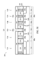
- FIGS. 3A-3F show cross-section views taken along the line a-a of FIG. 2C at various stages of fabrication according to various aspects of the present disclosure
- FIG. 4A-4B shows top views of a portion of one of the CMOS semiconductor dies in the exemplary wafer of FIGS. 2A and 2B according to various aspects of the present disclosure.
- FIG. 5A-5B shows top views of a portion of one of the CMOS semiconductor dies in the exemplary wafer of FIGS. 2A and 2B according to various aspects of the present disclosure.
- first and second features are formed in direct contact
- additional features may be formed between the first and second features, such that the first and second features may not be in direct contact
- Various features may be arbitrarily drawn in different scales for simplicity and clarity. Further, the present disclosure may repeat reference numerals and/or letters in the various examples.
- FIG. 1 is a flowchart illustrating a method 100 of fabricating a complementary metal-oxide-semiconductor (CMOS) semiconductor die according to various aspects of the present disclosure.
- FIG. 2A shows a top view of an exemplary wafer 20 having a plurality of individual CMOS semiconductor dies 200 according to various aspects of the present disclosure
- FIG. 2B shows a top view of a portion of the exemplary wafer 200 of FIG. 2A according to various aspects of the present disclosure
- FIG. 2C shows a top view of a portion of one of the CMOS semiconductor dies 200 in the exemplary wafer 20 of FIGS. 2A and 2B according to various aspects of the present disclosure
- FIGS. 1 through 3F show cross-section views taken along the line a-a of FIG. 2C at various stages of fabrication according to various aspects of the present disclosure.
- part of the semiconductor die 200 may be fabricated with CMOS technology processing. Accordingly, it is understood that additional processes may be provided before, during, and after the method 100 of FIG. 1 , and that some other processes may only be briefly described herein.
- FIGS. 1 through 3F are simplified for a better understanding of the concepts of the present disclosure.
- the figures illustrate metal gate electrodes for the semiconductor die 200 , it is understood the semiconductor die 200 may be part of an integrated circuit (IC) that may comprise a number of other devices comprising resistors, capacitors, inductors, fuses, etc.
- IC integrated circuit
- FIG. 2A illustrates the exemplary wafer 20 having the plurality of individual CMOS semiconductor dies 200 fabricated by a “gate last” process.
- FIG. 2B illustrates a portion of the exemplary wafer 20 of FIG. 2A comprising the exemplary semiconductor die 200 , wherein the semiconductor die 200 comprises various conductive regions comprising a first conductive region 200 a and a second conductive region 200 b.
- the semiconductor die 200 comprises an insulation layer 224 over a major surface 202 s of a substrate 202 (shown in FIGS. 3A-3F ).
- FIG. 2C illustrates a portion of the semiconductor die 200 following the “gate last” process to form the first conductive region 200 a with a plurality of conductive structures (e.g., P-metal gate features 200 p , N-metal gate features 200 n , resistor features 200 r , etc.) within the insulation layer 224 .
- a plurality of conductive structures e.g., P-metal gate features 200 p , N-metal gate features 200 n , resistor features 200 r , etc.
- the plurality of conductive structures is electrically coupled with one or more electrical components (e.g., comprising but not limited to resistors, capacitors, inductors, transistors, diodes, etc., not shown) in the semiconductor die 200 for interconnecting such components to form a desired circuit.
- electrical components e.g., comprising but not limited to resistors, capacitors, inductors, transistors, diodes, etc., not shown
- the P-metal gate features 200 p comprise a plurality of P-metal gate areas 200 pa , 200 pb , 200 pc , and 200 pd while the N-metal gate features 200 n comprise a plurality of N-metal gate areas 200 na , 200 nb , 200 nc , and 200 nd .
- the plurality of P-metal gate areas 200 pa , 200 pb , 200 pc , and 200 pd formed within the insulation layer 224 is collectively covering a first area of the major surface 202 s while the plurality of N-metal gate areas 200 na , 200 nb , 200 nc , and 200 nd formed within the insulation layer 224 is collectively covering a second area of the major surface 202 s , wherein a first ratio of the first area to the second area is equal to or greater than 1. In one embodiment, the first ratio is from 1 to 3.
- the resistor features 200 r comprise a plurality of resistor areas (also referred as 200 r ) formed within the insulation layer 224 , collectively covering a fifth area of the major surface 202 s .
- a third ratio of the fifth area to a sum of the first area and second area is less than 0.05.
- the illustrated portion of the semiconductor die 200 in FIG. 2C also comprises the second conductive region 200 b with a plurality of dummy conductive structures (e.g., dummy P-metal gate features 300 p , dummy N-metal gate features 300 n , dummy resistor features 300 r , etc.) within the insulation layer 224 .
- the plurality of dummy conductive structures is electrically isolated from one or more electrical components (e.g., comprising but not limited to resistors, capacitors, inductors, transistors, diodes, etc., not shown) in the semiconductor die 200 for improving non-uniform distribution of metal gate electrodes to form a desired circuit.
- the dummy P-metal gate features 300 p comprise a plurality of dummy P-metal gate areas 300 pa , 300 pb , 300 pc , 300 pd , 300 pe , 300 pf and 300 pg while the dummy N-metal gate features 300 n comprise a plurality of dummy N-metal gate areas 300 na , 300 nb , 300 nc , and 300 nd .
- the plurality of dummy P-metal gate areas 300 pa , 300 pb , 300 pc , 300 pd , 300 pe , 300 pf and 300 pg formed within the insulation layer 224 is collectively covering a third area of the major surface 202 s while the plurality of dummy N-metal gate areas 300 na , 300 nb , 300 nc , and 300 nd formed within the insulation layer 224 is collectively covering a fourth area of the major surface 202 s , wherein a second ratio of the third area to the fourth area is substantially equal to the first ratio. In one embodiment, the second ratio is from 1 to 3.
- the dummy resistor features 300 r comprises a plurality of dummy resistor areas (also referred as 300 r ) formed within the insulation layer 224 collectively covering a sixth area of the major surface 202 s .
- a fourth ratio of the sixth area to a sum of the third area and fourth area is less than 0.05.
- each of the plurality of dummy P-metal gate areas 300 pa , 300 pb , 300 pc , 300 pd , 300 pe , 300 pf and 300 pg has a similar shape to the other dummy P-metal gate areas 300 pa , 300 pb , 300 pc , 300 pd , 300 pe , 300 pf and 300 pg .
- each of the plurality of dummy P-metal gate areas 300 pa , 300 pb , 300 pc , 300 pd , 300 pe , 300 pf and 300 pg is of similar size.
- each of the plurality of dummy N-metal gate areas 300 na , 300 nb , 300 nc , and 300 nd has a similar shape to the other dummy N-metal gate areas 300 na , 300 nb , 300 nc , and 300 nd .
- each of the plurality of dummy N-metal gate areas 300 na , 300 nb , 300 nc , and 300 nd is of similar size.
- each of the plurality of dummy P-metal gate areas 300 pa , 300 pb , 300 pc , 300 pd , 300 pe , 300 pf and 300 pg has a similar shape to each of the plurality of dummy N-metal gate areas 300 na , 300 nb , 300 nc , and 300 nd .
- each of the plurality of dummy P-metal gate areas 300 pa , 300 pb , 300 pc , 300 pd , 300 pe , 300 pf and 300 pg has a similar size to each of the plurality of dummy N-metal gate areas 300 na , 300 nb , 300 nc , and 300 nd.
- one (e.g., 300 nc ) of the plurality of dummy N-metal gate areas 300 na , 300 nb , 300 nc , and 300 nd is between two of the dummy P-metal gate areas (e.g. 300 pb and 300 pd ).
- one (e.g., 300 pc ) of the plurality of dummy P-metal gate areas 300 pa , 300 pb , 300 pc , 300 pd , 300 pe , 300 pf and 300 pg is between two of the dummy
- N-metal gate areas e.g., 300 nb and 300 nd .
- one (e.g., 300 nb ) of the plurality of dummy N-metal gate areas is between one (e.g., 300 pb ) of the dummy P-metal gate areas and one (e.g., 200 pb ) of the plurality of P-metal gate areas.
- one (e.g. 300 pc ) of the plurality of dummy P-metal gate areas is between one (e.g., 300 nc ) of the dummy N-metal gate areas and one (e.g., 200 nc ) of the plurality of N-metal gate areas.
- the method 100 begins with step 102 in which a substrate 202 comprising a major surface 202 s is provided, wherein the substrate 202 comprises the first conductive region 200 a and the second conductive region 200 b .
- the substrate 202 may comprise a silicon substrate.
- the substrate 202 may alternatively comprise silicon germanium, gallium arsenic, or other suitable semiconductor materials.
- the substrate 202 may further comprise other features such as various doped regions, a buried layer, and/or an epitaxial (epi) layer.
- the substrate 202 may be a semiconductor on insulator such as silicon on insulator (SOI).
- the semiconductor substrate 202 may comprise a doped epi layer, a gradient semiconductor layer, and/or may further include a semiconductor layer overlying another semiconductor layer of a different type such as a silicon layer on a silicon germanium layer.
- a compound semiconductor substrate may comprise a multilayer silicon structure or a silicon substrate may include a multilayer compound semiconductor structure.
- isolation regions such as shallow trench isolation (STI) may be formed on the substrate 202 to define and electrically isolate the various active regions from each other.
- the isolation regions may comprise materials such as silicon oxide, silicon nitride, silicon oxynitride, fluoride-doped silicate glass (FSG), a low-k dielectric material, and/or combinations thereof.
- the STI may be formed by any suitable process.
- the formation of the STI may include patterning the semiconductor substrate by a photolithography process, etching a trench in the substrate (for example, by using a dry etching, wet etching, and/or plasma etching process), and filling the trench (for example, by using a chemical vapor deposition process) with a dielectric material.
- the filled trench may have a multi-layer structure such as a thermal oxide liner layer filled with silicon nitride or silicon oxide.
- the first conductive region 200 a comprises a first STI 204 a and a second STI 204 b , wherein the second STI 204 b isolates a P-active region 206 p and an N-active region 206 n .
- the second conductive region 200 b comprises a third STI 304 b and a fourth STI 304 a , wherein the third STI 304 b isolates a P-active region 306 p and an N-active region 306 n .
- the second conductive region 200 b may fully comprise a STI (not shown).
- the P-active regions 206 p , 306 p and N-active regions 206 n , 306 n may comprise various doping configurations depending on design requirements.
- the P-active regions 206 p , 306 p are doped with n-type dopants, such as phosphorus or arsenic;
- the N-active regions 206 n , 306 n are doped with p-type dopants, such as boron or BF 2 .
- the P-active regions 206 p , 306 p may act as regions configured for p-type metal-oxide-semiconductor field-effect transistors (referred to as pMOSFETs); the N-active regions 206 n and 306 n may act as regions configured for n-type metal-oxide-semiconductor field-effect transistors (referred to as nMOSFETs).
- pMOSFETs p-type metal-oxide-semiconductor field-effect transistors
- nMOSFETs n-type metal-oxide-semiconductor field-effect transistors
- step 104 in which the structure in FIG. 3B is produced by forming a plurality of dummy gate electrodes 210 (denoted as 210 p , 210 n , 210 r , 310 p , 310 n , and 310 r ) within an insulation layer 224 over the major surface 202 s of the substrate 202 .
- some dummy gate electrodes 210 p , 210 n , and 210 r are located in the first conductive region 200 a while some dummy gate electrodes 310 p , 310 n , and 310 r are located in the second conductive region 200 b .
- a first subset (e.g., 210 p and 310 p ) of the dummy gate electrodes 210 is formed over the P-active regions 206 p , 306 p while a second subset (e.g., 210 n and 310 n ) of the dummy gate electrodes 210 is formed over the N-active regions 206 n , 306 n .
- a third subset (e.g., 210 r and 310 r ) of the dummy gate electrodes 210 is formed over the STIs 204 a , 304 a .
- the dummy gate electrode 210 r may comprise a first portion 210 ra , a second portion 210 rb , and a third portion 210 rc between the first portion 210 ra and the second portion 210 rb.
- a gate dielectric layer 212 is formed over the substrate 202 .
- the gate dielectric layer 212 may comprise silicon oxide, silicon nitride, silicon oxynitride, or high-k dielectric.
- High-k dielectrics comprise certain metal oxides. Examples of metal oxides used for high-k dielectrics include oxides of Li, Be, Mg, Ca, Sr, Sc, Y, Zr, Hf, Al, La, Ce, Pr, Nd, Sm, Eu, Gd, Tb, Dy, Ho, Er, Tm, Yb, Lu, and mixtures thereof.
- the gate dielectric layer 212 is a high-k dielectric layer comprising HfO x with a thickness in the range of about 10 to 30 angstroms.
- the gate dielectric layer 212 may be formed using a suitable process such as atomic layer deposition (ALD), chemical vapor deposition (CVD), physical vapor deposition (PVD), thermal oxidation, UV-ozone oxidation, or combinations thereof.
- the gate dielectric layer 212 may further comprise an interfacial layer (not shown) to reduce damage between the gate dielectric layer 212 and the substrate 202 .
- the interfacial layer may comprise silicon oxide.
- a TiN layer 214 is deposited over the gate dielectric layer 212 to reduce Al atomic diffusion of an N-metal gate electrode to the gate dielectric layer 212 .
- the TiN layer 214 may also act as a portion of a resistor.
- the TiN layer 214 has a thickness ranging from 5 to 15 angstroms.
- the TiN layer 214 may be formed by CVD, PVD or other suitable technique.
- a dummy gate electrode 216 is subsequently formed over the TiN layer 214 .
- the dummy gate electrode 216 may comprise a single layer or multilayer structure.
- the dummy gate electrode 216 may comprise poly-silicon.
- the dummy gate electrode 216 may be doped poly-silicon with the uniform or gradient doping.
- the dummy gate electrode 216 may have a thickness in the range of about 30 nm to about 60 nm.
- the dummy gate electrode 216 may be formed using a low-pressure chemical vapor deposition (LPCVD) process or a plasma-enhanced chemical vapor deposition (PECVD) process.
- LPCVD low-pressure chemical vapor deposition
- PECVD plasma-enhanced chemical vapor deposition
- the dummy gate electrode 216 , TiN layer 214 and gate dielectric layer 212 are patterned to produce the structure shown in FIG. 3B .
- a layer of photoresist (not shown) is formed over the dummy gate electrode 216 by a suitable process, such as spin-on coating, and patterned to form a patterned photoresist feature over the dummy gate electrode 216 by a proper lithography patterning method.
- a width of the patterned photoresist feature is in the range of about 10 to 45 nm.
- the patterned photoresist feature can then be transferred using a dry etching process to the underlying layers (i.e., the gate dielectric layer 212 , TiN layer 214 and dummy gate electrode 216 ) to form the plurality of the dummy gate electrodes 210 .
- the photoresist layer may be stripped thereafter.
- CMOS semiconductor die 200 may undergo other “gate last” processes and other CMOS technology processing to form various features of the CMOS semiconductor die 200 .
- the various components of the CMOS semiconductor die 200 may be formed prior to formation of P-metal gate features and N-metal gate features in a “gate last” process.
- the various components may comprise lightly doped source/drain regions (p-type and n-type LDD) and source/drain regions (p-type and n-type S/D) (not shown) in the active regions 206 p , 206 n , 306 p , and 306 n .
- the p-type LDD and S/D regions may be doped with B or In, and the n-type LDD and S/D regions may be doped with P or As.
- the various features may further comprise gate spacers 222 and the insulation layer 224 surrounding the plurality of the dummy gate electrodes 210 .
- the gate spacers 222 may be formed of silicon oxide, silicon nitride or other suitable materials.
- the insulation layer 224 may include an oxide formed by a high-aspect-ratio process (HARP) and/or a high-density-plasma (HDP) deposition process.
- the process steps up to this point have provided the plurality of the dummy gate electrodes 210 within the insulation layer 224 over the major surface 202 s of the substrate 202 .
- Some dummy gate electrodes 210 p and 210 r are protected while other dummy gate electrodes 210 n , 310 p , 310 n , and 310 r are simultaneously removed so that a plurality of resulting metal gate features may be formed in place of the dummy gate electrodes 210 n , 310 p , 310 n , and 310 r , i.e., a N-metal gate feature may be formed in place of the dummy gate electrode 210 n and a plurality of dummy N-metal gate features may be formed in place of the plurality of the dummy gate electrodes 310 p , 310 n , and 310 r .
- the dummy gate electrode 210 p is removed so that a P-metal gate feature may be formed in place of the dummy gate electrode 210 p .
- non-uniform distribution of the different metal gate features i.e., the P-metal gate features and the N-metal gate features
- CMP chemical-mechanical polishing
- the processing discussed below with reference to FIGS. 3C-3F may optimize distribution of the different metal gate electrodes by controlling a gate area ratio.
- the optimized distribution of the different metal gate electrodes can be more effective to prevent CMP loading effects for a gate-last process. Accordingly, Applicants' method of fabricating a CMOS semiconductor die may help the different metal gate electrodes maintain their uniformities, thereby reaching the CMOS performance.
- step 106 in which the structure in FIG. 3C is produced by removing the first subset (i.e. 210 p and 310 p ) of the plurality of the dummy gate electrodes 210 to form a first set of openings 208 p , 308 p , and optionally removing the first portion 210 ra and the second portion 210 rb of the dummy gate electrode 210 r to form a third set of openings 208 a , 208 b .
- the first subset i.e. 210 p and 310 p
- 210 p and 310 p ) of the plurality of the dummy gate electrodes 210 are removed to form the first set of openings 208 p , 308 p while the first portion 210 ra and the second portion 210 rb of the dummy gate electrode 210 r are removed to form the third set of openings 208 a , 208 b , while the dummy gate electrodes 210 n , 310 n , 310 r and the third portion 210 rc of the dummy gate electrode 210 r are covered by the patterned photo-sensitive layer 400 .
- the first subset (i.e., 210 p and 310 p ) of the plurality of the dummy gate electrodes 210 and the first portion 210 ra and the second portion 210 rb of the dummy gate electrode 210 r may be removed using a dry etch process.
- the dry etch process may be performed under a source power of about 650 to 800W, a bias power of about 100 to 120W, and a pressure of about 60 to 200 mTorr, using Cl 2 , HBr and He as etching gases.
- the patterned photo-sensitive layer 400 may be stripped thereafter.
- the method 100 in FIG. 1 continues with step 108 in which the structure in FIG. 3D is produced by filling the first subset of openings 208 p , 308 p with a first metal material 218 p to form a plurality of P-metal gate features 200 p , 300 p (i.e. P-metal gate area 200 pb and dummy P-metal gate area 300 pb in FIG. 2C ).
- the first metal material 218 p may comprise a P-work-function metal.
- the P-work-function metal comprises a metal selected from a group of TiN, WN, TaN, and Ru.
- the P-work-function metal may be formed by ALD, CVD or other suitable technique.
- the first metal material 218 p is first deposited to substantially fill the first set of openings 208 p , 308 p and the third set of openings 208 a , 208 b . Then, a CMP process is performed to remove a portion of the first metal material 218 p outside of the first set of openings 208 p , 308 p and the third set of openings 208 a , 208 b . Accordingly, the CMP process may stop when reaching the insulation layer 224 , and thus providing a substantially planar surface.
- the third set of openings 208 a , 208 b is filled with the first metal material 218 p to form conductive contacts of the resistor feature 200 r comprising a plurality of resistor areas 200 r .
- the plurality of resistor areas 200 r comprises poly-silicon 216 .
- the plurality of resistor areas 200 r comprises TiN 214 .
- the dummy resistor feature 300 r comprises a plurality of dummy resistor areas 300 r .
- the plurality of dummy resistor areas 300 r comprises poly-silicon 216 .
- the plurality of dummy resistor areas 300 r comprises TiN 214 .
- step 110 in which the structure in FIG. 3E is produced by removing the second subset (i.e., 210 n and 310 n ) of the plurality of the dummy gate electrodes 210 to form a second set of openings 208 n , 308 n .
- the second subset i.e., 210 n and 310 n
- the second subset (i.e., 210 n and 310 n ) of the plurality of the dummy gate electrodes 210 is removed to form the second set of openings 208 n , 308 n while the dummy gate electrode 310 r and the third portion 210 rc of the dummy gate electrode 210 r are covered by the patterned photo-sensitive layer 500 .
- the second subset (i.e., 210 n and 310 n ) of the plurality of the dummy gate electrodes 210 may be removed using a dry etch process.
- the dry etch process may be performed under a source power of about 650 to 800W, a bias power of about 100 to 120W, and a pressure of about 60 to 200 mTorr, using Cl 2 , HBr and He as etching gases.
- the patterned photo-sensitive layer 500 may be stripped thereafter.
- step 112 in which the structure in FIG. 3F is produced by filling the second subset of openings 208 n , 308 n with a second metal material 218 n to form a plurality of N-metal gate features 200 n , 300 n (i.e. N-metal gate area 200 nb and dummy N-metal gate area 300 nb in FIG. 2C ).
- the second metal material 218 n may comprise an N-work-function metal.
- the N-work-function metal comprises a material selected from a group of Ti, Ag, Al, TiAl, TiAlN, TaC, TaCN, TaSiN, Mn, and Zr.
- the N-work-function metal may be formed by ALD, PVD, sputtering or other suitable technique.
- the second metal material 218 n is first deposited to substantially fill the second set of openings 208 n , 308 n .
- a CMP process is performed to remove a portion of the second metal material 218 n outside of the second set of openings 208 n , 308 n . Accordingly, the CMP process may stop when reaching the insulation layer 224 , and thus providing a substantially planar surface.
- FIG. 4A-4B shows alternative top views of a portion of one of the CMOS semiconductor dies in the exemplary wafer of FIGS. 2A and 2B according to various aspects of the present disclosure.
- the second conductive region 200 b has a plurality of dummy conductive structures (e.g., dummy P-metal gate features 300 p , dummy N-metal gate features 300 n , etc.) within the insulation layer 224 , wherein each of the plurality of dummy P-metal gate areas 300 p has a similar shape and size to each of the plurality of dummy N-metal gate areas 300 n , wherein the distributions of the plurality of dummy P-metal gate areas 300 p and the plurality of dummy N-metal gate areas 300 n may be changed.
- dummy conductive structures e.g., dummy P-metal gate features 300 p , dummy N-metal gate features 300 n , etc.
- FIG. 5A-5B shows alternative top views of a portion of one of the CMOS semiconductor dies in the exemplary wafer of FIGS. 2A and 2B according to various aspects of the present disclosure.
- the second conductive region 200 b has a plurality of dummy conductive structures (e.g., dummy P-metal gate features 300 p , dummy N-metal gate features 300 n , etc.) within the insulation layer 224 , wherein each of the plurality of dummy P-metal gate areas 300 p may have a different shape and size to each of the plurality of dummy N-metal gate areas 300 n , wherein the distributions of the plurality of dummy P-metal gate areas 300 p and the plurality of dummy N-metal gate areas 300 n may be changed.
- dummy conductive structures e.g., dummy P-metal gate features 300 p , dummy N-metal gate features 300 n , etc.
- CMOS semiconductor die 200 may undergo further CMOS processes to form various features such as contacts/vias, interconnect metal layers, dielectric layers, passivation layers, etc.
- a CMOS semiconductor die comprises a substrate; an insulation layer over a major surface of the substrate; a plurality of P-metal gate areas formed within the insulation layer collectively covering a first area of the major surface; a plurality of N-metal gate areas formed within the insulation layer collectively covering a second area of the major surface, wherein a first ratio of the first area to the second area is equal to or greater than 1; a plurality of dummy P-metal gate areas formed within the insulation layer collectively covering a third area of the major surface; and a plurality of dummy N-metal gate areas formed within the insulation layer collectively covering a fourth area of the major surface, wherein a second ratio of the third area to the fourth area is substantially equal to the first ratio.
- a CMOS semiconductor die comprises a substrate; an insulation layer over a major surface of the substrate; a plurality of P-metal gate areas formed within the insulation layer collectively covering a first area of the major surface; a plurality of N-metal gate areas formed within the insulation layer collectively covering a second area of the major surface, wherein a first ratio of the first area to the second area is equal to or greater than 1; a plurality of dummy P-metal gate areas formed within the insulation layer collectively covering a third area of the major surface; a plurality of dummy N-metal gate areas formed within the insulation layer collectively covering a fourth area of the major surface, wherein a second ratio of the third area to the fourth area is substantially equal to the first ratio; a plurality of resistor areas formed within the insulation layer collectively covering a fifth area of the major surface, wherein a third ratio of the fifth area to a sum of the first area and second area is less than 0.05; and a plurality of dummy
Landscapes
- Engineering & Computer Science (AREA)
- Power Engineering (AREA)
- Microelectronics & Electronic Packaging (AREA)
- Computer Hardware Design (AREA)
- General Physics & Mathematics (AREA)
- Physics & Mathematics (AREA)
- Condensed Matter Physics & Semiconductors (AREA)
- Manufacturing & Machinery (AREA)
- Ceramic Engineering (AREA)
- General Engineering & Computer Science (AREA)
- Chemical & Material Sciences (AREA)
- Composite Materials (AREA)
- Materials Engineering (AREA)
- Metal-Oxide And Bipolar Metal-Oxide Semiconductor Integrated Circuits (AREA)
Priority Applications (8)
| Application Number | Priority Date | Filing Date | Title |
|---|---|---|---|
| US13/312,306 US9006860B2 (en) | 2011-12-06 | 2011-12-06 | Metal gate features of semiconductor die |
| KR1020120029600A KR101338664B1 (ko) | 2011-12-06 | 2012-03-22 | 반도체 다이의 금속 게이트 피처 |
| CN201210107453.5A CN103151353B (zh) | 2011-12-06 | 2012-04-12 | 半导体管芯的金属栅极部件 |
| TW101113429A TWI523198B (zh) | 2011-12-06 | 2012-04-16 | Cmos半導體晶片 |
| US14/496,399 US10026656B2 (en) | 2011-12-06 | 2014-09-25 | Metal gate features of semiconductor die |
| US14/665,547 US9209090B2 (en) | 2011-12-06 | 2015-03-23 | Method of forming a semiconductor die |
| US14/955,690 US9515069B2 (en) | 2011-12-06 | 2015-12-01 | Semiconductor die |
| US15/365,457 US10672760B2 (en) | 2011-12-06 | 2016-11-30 | Semiconductor die |
Applications Claiming Priority (1)
| Application Number | Priority Date | Filing Date | Title |
|---|---|---|---|
| US13/312,306 US9006860B2 (en) | 2011-12-06 | 2011-12-06 | Metal gate features of semiconductor die |
Related Child Applications (2)
| Application Number | Title | Priority Date | Filing Date |
|---|---|---|---|
| US14/496,399 Continuation-In-Part US10026656B2 (en) | 2011-12-06 | 2014-09-25 | Metal gate features of semiconductor die |
| US14/665,547 Continuation US9209090B2 (en) | 2011-12-06 | 2015-03-23 | Method of forming a semiconductor die |
Publications (2)
| Publication Number | Publication Date |
|---|---|
| US20130140641A1 US20130140641A1 (en) | 2013-06-06 |
| US9006860B2 true US9006860B2 (en) | 2015-04-14 |
Family
ID=48523387
Family Applications (4)
| Application Number | Title | Priority Date | Filing Date |
|---|---|---|---|
| US13/312,306 Active 2032-02-25 US9006860B2 (en) | 2011-12-06 | 2011-12-06 | Metal gate features of semiconductor die |
| US14/665,547 Active US9209090B2 (en) | 2011-12-06 | 2015-03-23 | Method of forming a semiconductor die |
| US14/955,690 Active US9515069B2 (en) | 2011-12-06 | 2015-12-01 | Semiconductor die |
| US15/365,457 Active US10672760B2 (en) | 2011-12-06 | 2016-11-30 | Semiconductor die |
Family Applications After (3)
| Application Number | Title | Priority Date | Filing Date |
|---|---|---|---|
| US14/665,547 Active US9209090B2 (en) | 2011-12-06 | 2015-03-23 | Method of forming a semiconductor die |
| US14/955,690 Active US9515069B2 (en) | 2011-12-06 | 2015-12-01 | Semiconductor die |
| US15/365,457 Active US10672760B2 (en) | 2011-12-06 | 2016-11-30 | Semiconductor die |
Country Status (4)
| Country | Link |
|---|---|
| US (4) | US9006860B2 (ko) |
| KR (1) | KR101338664B1 (ko) |
| CN (1) | CN103151353B (ko) |
| TW (1) | TWI523198B (ko) |
Cited By (1)
| Publication number | Priority date | Publication date | Assignee | Title |
|---|---|---|---|---|
| US10431583B2 (en) | 2016-02-11 | 2019-10-01 | Samsung Electronics Co., Ltd. | Semiconductor device including transistors with adjusted threshold voltages |
Families Citing this family (16)
| Publication number | Priority date | Publication date | Assignee | Title |
|---|---|---|---|---|
| US8735994B2 (en) * | 2012-03-27 | 2014-05-27 | Taiwan Semiconductor Manufacturing Company, Ltd. | Electrical-free dummy gate |
| KR102311552B1 (ko) | 2014-12-04 | 2021-10-12 | 삼성전자주식회사 | 반도체 소자 및 그 제조 방법 |
| US9640438B2 (en) * | 2014-12-30 | 2017-05-02 | Globalfoundries Singapore Pte. Ltd. | Integrated circuits with inactive gates and methods of manufacturing the same |
| US9530772B1 (en) * | 2015-08-06 | 2016-12-27 | International Business Machines Corporation | Methods of manufacturing devices including gates with multiple lengths |
| US10103027B2 (en) * | 2016-06-20 | 2018-10-16 | Applied Materials, Inc. | Hydrogenation and nitridization processes for modifying effective oxide thickness of a film |
| US10510545B2 (en) | 2016-06-20 | 2019-12-17 | Applied Materials, Inc. | Hydrogenation and nitridization processes for modifying effective oxide thickness of a film |
| US10388576B2 (en) * | 2016-06-30 | 2019-08-20 | International Business Machines Corporation | Semiconductor device including dual trench epitaxial dual-liner contacts |
| US20180337033A1 (en) * | 2017-05-16 | 2018-11-22 | Globalfoundries Inc. | Novel approach to improve sdb device performance |
| US10727223B2 (en) * | 2017-11-13 | 2020-07-28 | Taiwan Semiconductor Manufacturing Co., Ltd. | Thin film resistor |
| DE102018125043B4 (de) | 2017-11-13 | 2023-01-19 | Taiwan Semiconductor Manufacturing Co. Ltd. | Neuartiger Dünnfilmwiderstand und Verfahren zu dessen Herstellung |
| CN110233151B (zh) * | 2018-10-30 | 2021-10-01 | 上海权策微电子技术有限公司 | 一种cmos管及其制造方法 |
| WO2020146030A1 (en) * | 2019-01-09 | 2020-07-16 | Applied Materials, Inc. | Hydrogenation and nitridization processes for modifying effective oxide thickness of a film |
| US11257816B2 (en) * | 2019-08-20 | 2022-02-22 | Taiwan Semiconductor Manufacturing Co., Ltd. | Method for manufacturing semiconductor device including dummy gate electrodes |
| WO2021150625A1 (en) | 2020-01-23 | 2021-07-29 | Applied Materials, Inc. | Method of cleaning a structure and method of depositiing a capping layer in a structure |
| US20220037312A1 (en) * | 2020-07-29 | 2022-02-03 | Taiwan Semiconductor Manufacturing Co., Ltd. | Integrated circuit device, method, layout, and system |
| CN117406547B (zh) * | 2023-12-15 | 2024-04-05 | 合肥晶合集成电路股份有限公司 | 一种光罩的伪图形结构及光罩 |
Citations (8)
| Publication number | Priority date | Publication date | Assignee | Title |
|---|---|---|---|---|
| US5493135A (en) * | 1993-08-26 | 1996-02-20 | Aspec Technology, Inc. | Symmetrical multi-layer metal logic array with continuous substrate taps and extension portions for increased gate density |
| US20020058374A1 (en) * | 2000-11-16 | 2002-05-16 | Tae-Kyun Kim | Method of forming dual-metal gates in semiconductor device |
| KR20060134010A (ko) | 2004-04-30 | 2006-12-27 | 마츠시타 덴끼 산교 가부시키가이샤 | 반도체의 제조 방법 및 반도체 장치 |
| JP2007250705A (ja) | 2006-03-15 | 2007-09-27 | Nec Electronics Corp | 半導体集積回路装置及びダミーパターンの配置方法 |
| JP2007311818A (ja) | 2007-07-18 | 2007-11-29 | Renesas Technology Corp | 半導体装置 |
| US20080003734A1 (en) * | 2006-06-29 | 2008-01-03 | Harry Chuang | Selective formation of stress memorization layer |
| US20090090977A1 (en) * | 2007-10-09 | 2009-04-09 | International Business Machines Corporation | Resistor and fet formed from the metal portion of a mosfet metal gate stack |
| JP2010206198A (ja) | 2009-02-27 | 2010-09-16 | Taiwan Semiconductor Manufacturing Co Ltd | トランジスタ性能に対するシャロートレンチアイソレーション(sti)の応力変動を低減するダミーフィル |
Family Cites Families (12)
| Publication number | Priority date | Publication date | Assignee | Title |
|---|---|---|---|---|
| JP2689871B2 (ja) * | 1993-11-10 | 1997-12-10 | 日本電気株式会社 | 3値入力バッファ回路 |
| US5907867A (en) * | 1994-09-09 | 1999-05-25 | Hitachi, Ltd. | Translation lookaside buffer supporting multiple page sizes |
| JP3014025B2 (ja) * | 1995-03-30 | 2000-02-28 | 日本電気株式会社 | BiCMOS論理集積回路 |
| JP2720816B2 (ja) * | 1995-03-31 | 1998-03-04 | 日本電気株式会社 | BiMOS集積回路 |
| JP3726760B2 (ja) * | 2002-02-20 | 2005-12-14 | セイコーエプソン株式会社 | 半導体装置の製造方法 |
| US20080076216A1 (en) * | 2006-09-25 | 2008-03-27 | Sangwoo Pae | Method to fabricate high-k/metal gate transistors using a double capping layer process |
| US8125051B2 (en) * | 2008-07-03 | 2012-02-28 | Taiwan Semiconductor Manufacturing Company, Ltd. | Device layout for gate last process |
| US8237227B2 (en) * | 2008-08-29 | 2012-08-07 | Taiwan Semiconductor Manufacturing Company, Ltd. | Dummy gate structure for gate last process |
| JP5586628B2 (ja) * | 2008-11-17 | 2014-09-10 | イントリンシツク・イー・デー・ベー・ベー | 分散puf |
| US8193900B2 (en) * | 2009-06-24 | 2012-06-05 | United Microelectronics Corp. | Method for fabricating metal gate and polysilicon resistor and related polysilicon resistor structure |
| US8890260B2 (en) * | 2009-09-04 | 2014-11-18 | Taiwan Semiconductor Manufacturing Company, Ltd. | Polysilicon design for replacement gate technology |
| US10026656B2 (en) | 2011-12-06 | 2018-07-17 | Taiwan Semiconductor Manufacturing Company, Ltd. | Metal gate features of semiconductor die |
-
2011
- 2011-12-06 US US13/312,306 patent/US9006860B2/en active Active
-
2012
- 2012-03-22 KR KR1020120029600A patent/KR101338664B1/ko active IP Right Grant
- 2012-04-12 CN CN201210107453.5A patent/CN103151353B/zh active Active
- 2012-04-16 TW TW101113429A patent/TWI523198B/zh active
-
2015
- 2015-03-23 US US14/665,547 patent/US9209090B2/en active Active
- 2015-12-01 US US14/955,690 patent/US9515069B2/en active Active
-
2016
- 2016-11-30 US US15/365,457 patent/US10672760B2/en active Active
Patent Citations (9)
| Publication number | Priority date | Publication date | Assignee | Title |
|---|---|---|---|---|
| US5493135A (en) * | 1993-08-26 | 1996-02-20 | Aspec Technology, Inc. | Symmetrical multi-layer metal logic array with continuous substrate taps and extension portions for increased gate density |
| US20020058374A1 (en) * | 2000-11-16 | 2002-05-16 | Tae-Kyun Kim | Method of forming dual-metal gates in semiconductor device |
| KR20060134010A (ko) | 2004-04-30 | 2006-12-27 | 마츠시타 덴끼 산교 가부시키가이샤 | 반도체의 제조 방법 및 반도체 장치 |
| JP2007250705A (ja) | 2006-03-15 | 2007-09-27 | Nec Electronics Corp | 半導体集積回路装置及びダミーパターンの配置方法 |
| US7772070B2 (en) | 2006-03-15 | 2010-08-10 | Nec Electronics Corporation | Semiconductor integrated circuit device and dummy pattern arrangement method |
| US20080003734A1 (en) * | 2006-06-29 | 2008-01-03 | Harry Chuang | Selective formation of stress memorization layer |
| JP2007311818A (ja) | 2007-07-18 | 2007-11-29 | Renesas Technology Corp | 半導体装置 |
| US20090090977A1 (en) * | 2007-10-09 | 2009-04-09 | International Business Machines Corporation | Resistor and fet formed from the metal portion of a mosfet metal gate stack |
| JP2010206198A (ja) | 2009-02-27 | 2010-09-16 | Taiwan Semiconductor Manufacturing Co Ltd | トランジスタ性能に対するシャロートレンチアイソレーション(sti)の応力変動を低減するダミーフィル |
Non-Patent Citations (1)
| Title |
|---|
| Notice of Allowance dated Sep. 12, 2013 with English translation from corresponding application No. KR 10-2012-0029600. |
Cited By (1)
| Publication number | Priority date | Publication date | Assignee | Title |
|---|---|---|---|---|
| US10431583B2 (en) | 2016-02-11 | 2019-10-01 | Samsung Electronics Co., Ltd. | Semiconductor device including transistors with adjusted threshold voltages |
Also Published As
| Publication number | Publication date |
|---|---|
| CN103151353B (zh) | 2016-06-29 |
| US20150194352A1 (en) | 2015-07-09 |
| US20160093610A1 (en) | 2016-03-31 |
| US20130140641A1 (en) | 2013-06-06 |
| CN103151353A (zh) | 2013-06-12 |
| TW201324745A (zh) | 2013-06-16 |
| TWI523198B (zh) | 2016-02-21 |
| KR20130063443A (ko) | 2013-06-14 |
| US9209090B2 (en) | 2015-12-08 |
| US9515069B2 (en) | 2016-12-06 |
| KR101338664B1 (ko) | 2013-12-06 |
| US20170084608A1 (en) | 2017-03-23 |
| US10672760B2 (en) | 2020-06-02 |
Similar Documents
| Publication | Publication Date | Title |
|---|---|---|
| US10672760B2 (en) | Semiconductor die | |
| US11894443B2 (en) | Method of making gate structure of a semiconductor device | |
| US11670711B2 (en) | Metal gate electrode of a semiconductor device | |
| US11393726B2 (en) | Metal gate structure of a CMOS semiconductor device and method of forming the same | |
| US8304842B2 (en) | Interconnection structure for N/P metal gates | |
| US8183644B1 (en) | Metal gate structure of a CMOS semiconductor device | |
| US8378428B2 (en) | Metal gate structure of a semiconductor device | |
| US10026656B2 (en) | Metal gate features of semiconductor die |
Legal Events
| Date | Code | Title | Description |
|---|---|---|---|
| AS | Assignment |
Owner name: TAIWAN SEMICONDUCTOR MANUFACTURING COMPANY, LTD., Free format text: ASSIGNMENT OF ASSIGNORS INTEREST;ASSIGNORS:CHUANG, HARRY-HAK-LAY;ZHU, MING;REEL/FRAME:027335/0249 Effective date: 20111130 |
|
| STCF | Information on status: patent grant |
Free format text: PATENTED CASE |
|
| MAFP | Maintenance fee payment |
Free format text: PAYMENT OF MAINTENANCE FEE, 4TH YEAR, LARGE ENTITY (ORIGINAL EVENT CODE: M1551); ENTITY STATUS OF PATENT OWNER: LARGE ENTITY Year of fee payment: 4 |
|
| MAFP | Maintenance fee payment |
Free format text: PAYMENT OF MAINTENANCE FEE, 8TH YEAR, LARGE ENTITY (ORIGINAL EVENT CODE: M1552); ENTITY STATUS OF PATENT OWNER: LARGE ENTITY Year of fee payment: 8 |