US8994634B2 - Display device - Google Patents
Display device Download PDFInfo
- Publication number
- US8994634B2 US8994634B2 US13/563,392 US201213563392A US8994634B2 US 8994634 B2 US8994634 B2 US 8994634B2 US 201213563392 A US201213563392 A US 201213563392A US 8994634 B2 US8994634 B2 US 8994634B2
- Authority
- US
- United States
- Prior art keywords
- substrate
- bridge
- line
- gate
- lcd device
- Prior art date
- Legal status (The legal status is an assumption and is not a legal conclusion. Google has not performed a legal analysis and makes no representation as to the accuracy of the status listed.)
- Active, expires
Links
Images


Classifications
-
- G—PHYSICS
- G02—OPTICS
- G02F—OPTICAL DEVICES OR ARRANGEMENTS FOR THE CONTROL OF LIGHT BY MODIFICATION OF THE OPTICAL PROPERTIES OF THE MEDIA OF THE ELEMENTS INVOLVED THEREIN; NON-LINEAR OPTICS; FREQUENCY-CHANGING OF LIGHT; OPTICAL LOGIC ELEMENTS; OPTICAL ANALOGUE/DIGITAL CONVERTERS
- G02F1/00—Devices or arrangements for the control of the intensity, colour, phase, polarisation or direction of light arriving from an independent light source, e.g. switching, gating or modulating; Non-linear optics
- G02F1/01—Devices or arrangements for the control of the intensity, colour, phase, polarisation or direction of light arriving from an independent light source, e.g. switching, gating or modulating; Non-linear optics for the control of the intensity, phase, polarisation or colour
- G02F1/13—Devices or arrangements for the control of the intensity, colour, phase, polarisation or direction of light arriving from an independent light source, e.g. switching, gating or modulating; Non-linear optics for the control of the intensity, phase, polarisation or colour based on liquid crystals, e.g. single liquid crystal display cells
- G02F1/133—Constructional arrangements; Operation of liquid crystal cells; Circuit arrangements
- G02F1/1333—Constructional arrangements; Manufacturing methods
- G02F1/1345—Conductors connecting electrodes to cell terminals
- G02F1/13452—Conductors connecting driver circuitry and terminals of panels
-
- G—PHYSICS
- G02—OPTICS
- G02F—OPTICAL DEVICES OR ARRANGEMENTS FOR THE CONTROL OF LIGHT BY MODIFICATION OF THE OPTICAL PROPERTIES OF THE MEDIA OF THE ELEMENTS INVOLVED THEREIN; NON-LINEAR OPTICS; FREQUENCY-CHANGING OF LIGHT; OPTICAL LOGIC ELEMENTS; OPTICAL ANALOGUE/DIGITAL CONVERTERS
- G02F1/00—Devices or arrangements for the control of the intensity, colour, phase, polarisation or direction of light arriving from an independent light source, e.g. switching, gating or modulating; Non-linear optics
- G02F1/01—Devices or arrangements for the control of the intensity, colour, phase, polarisation or direction of light arriving from an independent light source, e.g. switching, gating or modulating; Non-linear optics for the control of the intensity, phase, polarisation or colour
- G02F1/13—Devices or arrangements for the control of the intensity, colour, phase, polarisation or direction of light arriving from an independent light source, e.g. switching, gating or modulating; Non-linear optics for the control of the intensity, phase, polarisation or colour based on liquid crystals, e.g. single liquid crystal display cells
- G02F1/133—Constructional arrangements; Operation of liquid crystal cells; Circuit arrangements
- G02F1/1333—Constructional arrangements; Manufacturing methods
- G02F1/1339—Gaskets; Spacers; Sealing of cells
-
- G—PHYSICS
- G02—OPTICS
- G02F—OPTICAL DEVICES OR ARRANGEMENTS FOR THE CONTROL OF LIGHT BY MODIFICATION OF THE OPTICAL PROPERTIES OF THE MEDIA OF THE ELEMENTS INVOLVED THEREIN; NON-LINEAR OPTICS; FREQUENCY-CHANGING OF LIGHT; OPTICAL LOGIC ELEMENTS; OPTICAL ANALOGUE/DIGITAL CONVERTERS
- G02F1/00—Devices or arrangements for the control of the intensity, colour, phase, polarisation or direction of light arriving from an independent light source, e.g. switching, gating or modulating; Non-linear optics
- G02F1/01—Devices or arrangements for the control of the intensity, colour, phase, polarisation or direction of light arriving from an independent light source, e.g. switching, gating or modulating; Non-linear optics for the control of the intensity, phase, polarisation or colour
- G02F1/13—Devices or arrangements for the control of the intensity, colour, phase, polarisation or direction of light arriving from an independent light source, e.g. switching, gating or modulating; Non-linear optics for the control of the intensity, phase, polarisation or colour based on liquid crystals, e.g. single liquid crystal display cells
- G02F1/133—Constructional arrangements; Operation of liquid crystal cells; Circuit arrangements
- G02F1/1333—Constructional arrangements; Manufacturing methods
- G02F1/1345—Conductors connecting electrodes to cell terminals
-
- G—PHYSICS
- G02—OPTICS
- G02F—OPTICAL DEVICES OR ARRANGEMENTS FOR THE CONTROL OF LIGHT BY MODIFICATION OF THE OPTICAL PROPERTIES OF THE MEDIA OF THE ELEMENTS INVOLVED THEREIN; NON-LINEAR OPTICS; FREQUENCY-CHANGING OF LIGHT; OPTICAL LOGIC ELEMENTS; OPTICAL ANALOGUE/DIGITAL CONVERTERS
- G02F1/00—Devices or arrangements for the control of the intensity, colour, phase, polarisation or direction of light arriving from an independent light source, e.g. switching, gating or modulating; Non-linear optics
- G02F1/01—Devices or arrangements for the control of the intensity, colour, phase, polarisation or direction of light arriving from an independent light source, e.g. switching, gating or modulating; Non-linear optics for the control of the intensity, phase, polarisation or colour
- G02F1/13—Devices or arrangements for the control of the intensity, colour, phase, polarisation or direction of light arriving from an independent light source, e.g. switching, gating or modulating; Non-linear optics for the control of the intensity, phase, polarisation or colour based on liquid crystals, e.g. single liquid crystal display cells
- G02F1/133—Constructional arrangements; Operation of liquid crystal cells; Circuit arrangements
- G02F1/1333—Constructional arrangements; Manufacturing methods
- G02F1/1335—Structural association of cells with optical devices, e.g. polarisers or reflectors
- G02F1/133509—Filters, e.g. light shielding masks
- G02F1/133512—Light shielding layers, e.g. black matrix
-
- G—PHYSICS
- G02—OPTICS
- G02F—OPTICAL DEVICES OR ARRANGEMENTS FOR THE CONTROL OF LIGHT BY MODIFICATION OF THE OPTICAL PROPERTIES OF THE MEDIA OF THE ELEMENTS INVOLVED THEREIN; NON-LINEAR OPTICS; FREQUENCY-CHANGING OF LIGHT; OPTICAL LOGIC ELEMENTS; OPTICAL ANALOGUE/DIGITAL CONVERTERS
- G02F2201/00—Constructional arrangements not provided for in groups G02F1/00 - G02F7/00
- G02F2201/12—Constructional arrangements not provided for in groups G02F1/00 - G02F7/00 electrode
Definitions
- the present disclosure relates to a display device, and more particularly, to a display device with enhanced aesthetic appearance.
- LCD devices are driven with a low operating voltage
- LCD devices have low power consumption and are used as portable devices. Accordingly, the LCD devices are widely applied to various fields such as notebook computers, monitors, spacecrafts, airplanes, etc.
- the LCD devices have been enlarged in size due to the decrease in weight and volume.
- research and development are being continuously done on a response time and image quality, leading to the much advance of quality.
- FIG. 1 is a sectional view schematically illustrating a related art LCD device.
- the related art LCD device includes a lower substrate 10 , an upper substrate 20 , a liquid crystal layer 30 , and a driver 40 .
- the lower substrate 10 faces the upper substrate 20 , and the liquid crystal layer 30 is formed between the lower substrate 10 and the upper substrate 20 .
- Various lines such as a gate line and a data line are formed on the lower substrate 10 .
- Various lines such as a gate line and a data line are formed on the lower substrate 10 .
- one side periphery area of the lower substrate 10 is exposed externally.
- the driver 40 is formed in the externally exposed one side periphery area of the lower substrate 10 , and supplies respective signals to a plurality of lines.
- the driver 40 includes a circuit film 41 , a Printed Circuit Board (PCB) 42 , and a driving chip 43 .
- the circuit film 41 is adhered to the lower substrate 10 at one end of the circuit film 41 , and the other end of the circuit film 41 is connected to the PCB 42 .
- the PCB 42 applies various signals to the lower substrate 10 through the circuit film 41 .
- a timing controller, various power source circuits, and a memory are mounted on the PCB 42 .
- the driving chip 43 is formed on the circuit film 41 and drives a plurality of data lines and gate lines.
- FIG. 2 is a plan view schematically illustrating a related art LCD device.
- FIG. 2A is a plan view schematically illustrating a related art lower substrate.
- FIG. 2B is a plan view schematically illustrating a related art upper substrate.
- the driver 40 supplies respective signals to the gate lines and data lines of the LCD device. Accordingly, the driver 40 is disposed at the left or right periphery portion of the LCD device for supplying respective signals to the gate lines, and disposed at the upper or lower periphery portion of the LCD device for supplying respective signals to the data lines.
- FIGS. 2A and 2B illustrate the GIP type LCD device.
- the related art lower substrate 10 includes a display area that displays an image and a non-display area that cannot display an image.
- a plurality of gate lines 12 and data lines 11 are intersected and formed, thereby defining a plurality of pixels.
- a thin film transistor T as a switching element is formed in each of the pixels.
- a plurality of elements for supplying signals to the display area are formed in the non-display area. Specifically, pads 13 a and 13 b , a signal line 14 , a GIP circuit block 15 , and a connection line 16 are formed in the non-display area.
- the pads 13 a and 13 b are connected to the driver 40 , and include a gate pad 13 a and a data pad 13 b.
- the gate pad 13 a and the signal line 14 are formed as one body, the signal line 14 is connected to the GIP circuit block 15 through the connection line 16 , and the GIP circuit block 15 is connected to the gate line 12 .
- the data pad 13 b is connected to the data line 11 .
- the related art upper substrate 20 includes a display area that displays an image and a non-display area that cannot display an image.
- Red (R), green (G), and blue (B) color filters 22 are formed in the display area.
- the color filters 22 are divided by a black matrix 24 .
- the black matrix 24 is formed in the non-display area, thereby preventing the leakage of light.
- the GIP circuit block 15 and the signal line 14 are complicatedly formed in the non-display area of the lower substrate 10 , the size of the non-display area increases inevitably, and thus, the size of the peripheral portion of the LCD device, namely, the size of the Bezel increases.
- a method of decreasing the GIP circuit block 15 area and a method of decreasing the signal line 14 area can be considered for reducing the size of the non-display area of the lower substrate 10 .
- a gate driver Integrated Circuit (IC) and a plurality of transistors for performing a portion of a gate PCB function are disposed in the GIP circuit block 15 area, and thus, it is actually difficult to reduce the GIP circuit block 15 area.
- the decrease in the width of the signal line 14 is required for reducing the signal line 14 area, but when decreasing the width of the signal line 14 , the resistance of the signal line 14 increases.
- the related art LCD device has limitations in reducing the size of the Bezel that is the peripheral portion thereof.
- a display device includes: first and second substrates facing each other; a plurality of gate lines and data lines formed on the first substrate to define a plurality of pixels by an intersection therebetween; a connection line formed on the first substrate to be electrically connected to the gate line; a signal line formed on the second substrate for supplying a signal to the gate line; and a first bridge formed on the second substrate for electrically connecting the signal line and the connection line.
- FIG. 1 is a sectional view schematically illustrating a related art LCD device
- FIG. 2A is a plan view schematically illustrating a lower substrate of the related art LCD device
- FIG. 2B is a plan view schematically illustrating a upper substrate of the related art LCD device
- FIG. 3A is a plan view illustrating a first substrate of an LCD device according to an embodiment of the present invention.
- FIG. 3B is a plan view illustrating a second substrate of an LCD device according to an embodiment of the present invention.
- FIG. 3C is a perspective view illustrating the first and second substrates of the LCD device shown in FIG. 3A and FIG. 3B ;
- FIG. 4 is a sectional view illustrating an LCD device according to an embodiment of the present invention, and corresponds to line A-B of FIGS. 3A and 3B ;
- FIG. 5 is a sectional view illustrating an LCD device according to another embodiment of the present invention, and corresponds to line A-B of FIGS. 3A and 3B ;
- FIG. 6 is a sectional view illustrating an LCD device according to another embodiment of the present invention, and corresponds to line A-B of FIGS. 3A and 3B ;
- FIG. 7 is a sectional view illustrating an LCD device according to another embodiment of the present invention, and corresponds to line A-B of FIGS. 3A and 3B ;
- FIG. 8A is a plan view illustrating a first substrate of an LCD device according to another embodiment of the present invention.
- FIG. 8B is a plan view illustrating a second substrate of an LCD device according to another embodiment of the present invention.
- FIG. 9A is a plan view illustrating a first substrate of an LCD device according to another embodiment of the present invention.
- FIG. 9B is a plan view illustrating a second substrate of an LCD device according to another embodiment of the present invention.
- FIG. 10 is a sectional view illustrating an LCD device according to another embodiment of the present invention, and corresponds to line A-B of FIGS. 9A and 9B ;
- FIG. 11 is a sectional view illustrating an LCD device according to another embodiment of the present invention, and corresponds to line C-D of FIGS. 9A and 9B ;
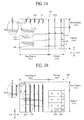
- FIGS. 12 and 13 are sectional views schematically illustrating an LCD device according to another embodiment of the present invention, and illustrate structures where a driver is additionally provided to a coupled substrate according to various embodiments;
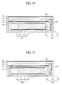
- FIGS. 14 and 15 are sectional views schematically illustrating an LCD device according to another embodiment of the present invention, and illustrate structures where a backlight unit is additionally coupled to a coupled substrate according to various embodiments.
- FIG. 3A is a plan view illustrating a first substrate of an LCD device according to an embodiment of the present invention.
- FIG. 3B is a plan view illustrating a second substrate of an LCD device according to an embodiment of the present invention.
- FIG. 3C is a perspective view illustrating the first and second substrates of the LCD device shown in FIG. 3A and FIG. 3B .
- the first substrate 100 includes a display area that displays an image and a non-display area that cannot display an image.
- a plurality of gate lines 110 and data lines 120 are intersected and formed, thereby defining a plurality of pixels.
- a thin film transistor T as a switching element is formed in each of the pixels.
- the gate lines 110 , the data lines 120 , and the thin film transistors T may be changed to various shapes as known to those skilled in the art.
- the data lines 120 may not be formed in a straight-line shape, or may be formed in a curve-line shape.
- pads 130 a and 130 b , a GIP circuit block 140 , and a connection line 150 are formed in the non-display area.
- the pads 130 a and 130 b are formed at one side end portion of the first substrate 100 , and a driver (not shown) is connected to the pads 130 a and 130 b.
- the pad 130 a is a gate pad 130 a for applying a signal to the gate line 110
- the pad 130 b is a data pad 130 b for applying a signal to the data line 110 .
- the data pad 130 b is directly connected to the data line 120 , but the gate pad 130 a is connected to the gate line 110 via various elements.
- an electrical connection between the gate pad 130 a and the gate line 110 is formed using an element that is formed at the below-described second substrate 200 , and thus, the size of the non-display area of the LCD device is reduced. That is, as described below, a plurality of signal lines for supplying signals to the gate lines 110 (which are formed on the first substrate 100 ) are formed on the second substrate 200 where the gate lines 110 are not formed, thus decreasing the size of the non-display area of the LCD device.
- a pad electrode 132 is formed at one end portion of the gate pad 130 a the pad electrode 132 is connected to the gate pad 130 a through a contact hole.
- the pad electrode 132 is exposed to the outside, and thus enables the gate pad 130 a to be easily connected to the below-described signal line (see reference numeral 260 of FIG. 3B ).
- the number and arrangement type of the gate pads 130 a may be changed variously according to the kind of an applied signal.
- a plurality of the GIP circuit blocks 140 are respectively disposed near the plurality of pixels, and each of the GIP circuit blocks 140 is connected to a corresponding gate line 110 .
- the GIP circuit block 140 is configured in a connection structure of a plurality of transistors, and the detailed configuration of the GIP circuit block 140 may be changed to various structures as known to those skilled in the art.
- connection line 150 is connected to the GIP circuit block 140 .
- a connection electrode 152 is formed at one end portion of the connection line 150 .
- the connection electrode is connected to the connection line 150 through a contact hole.
- the connection electrode 152 is exposed to the outside, and thus enables the connection line 150 to be easily connected to the below-described signal line (see reference numeral 260 of FIG. 3B ).
- the number and arrangement type of the connection lines 150 may be changed variously according to the kind of an applied signal.
- the pad electrode 132 formed at one end portion of the gate pad 130 a is not connected to the connection electrode 152 formed at one end portion of the connection line 150 , but an electrical connection between the pad electrode 132 and the connection electrode 152 may be realized by a structure that is formed on the below-described second substrate 200 .
- the substrate 200 includes a display area that displays an image and a non-display area that cannot display an image.
- Red (R), green (G), and blue (B) color filters 220 are formed in the display area.
- the color filters 220 are divided by a black matrix 240 .
- the kind and arrangement type of the black matrixes 240 may be variously changed as known to those skilled in the art.
- a plurality of signal lines 160 , first bridges 270 , and second bridges 280 are formed in the non-display area.
- a black matrix is entirely formed in the non-display area, thereby preventing the leakage of light.
- the black matrix includes a contact hole such that an electrical connection is formed between elements.
- the entire structure of the black matrix can be more easily understood with reference the below-described sectional structure of the LCD device.
- the signal line 260 is connected to the gate pad 130 a of FIG. 3A .
- the number of signal lines 260 corresponds to the number of gate pads 130 a .
- the signal lines 260 are arranged in the Y direction, and enable a gate signal to be applied to each of the gate lines 110 .
- the first bridge 270 connects the signal line 260 to the connection line 150 of FIG. 3A . That is, one end of the first bridge 270 is connected to the signal line 260 , and the other end of the first bridge 270 is connected to the connection electrode 152 . Accordingly, the signal line 260 is connected to the connection line 150 via the first bridge 270 and the connection electrode 152 .
- the second bridge 280 connects the signal line 260 to the gate pad 130 a of FIG. 3A . That is, one end of the second bridge 280 is connected to the signal line 260 , and the other end of the second bridge 280 is connected to the pad electrode 132 . Accordingly, the gate pad 130 a is connected to the signal line 260 via the pad electrode 132 and the second bridge 280 .
- the gate pad 130 a is connected to the GIP circuit block 140 sequentially via the pad electrode 132 , the second bridge 280 , the signal line 260 , the first bridge 270 , the connection electrode 152 , and the connection line 150 , and thus, a signal is transferred in the order of ⁇ circle around (1) ⁇ circle around (2) ⁇ circle around (3) ⁇ circle around (4) ⁇ circle around (5) ⁇ circle around (6) ⁇ circle around (7) ⁇ .
- FIG. 4 is a sectional view illustrating an LCD device according to an embodiment of the present invention, and corresponds to line A-B of FIGS. 3A and 3B .
- the LCD device includes a first substrate 100 and a second substrate 200 that face each other.
- a liquid crystal layer is formed between the first substrate 100 and the second substrate 200 , more specifically, between the two substrates 100 and 200 corresponding to the display area.
- the first substrate 100 may configure a lower substrate of the LCD device, and may be referred to as a thin film transistor substrate because a thin film transistor is formed thereon.
- a pad more specifically, a gate pad 130 a is formed on the first substrate 100 .
- a gate insulation layer 115 is formed on the gate pad 130 a.
- connection line 150 is formed on the gate insulation layer 115 , and a passivation layer 125 is formed on the connection line 150 .
- the connection line 150 and a data line may be formed of the same material and on the same layer, through the same process.
- the connection line 150 needs not necessarily be formed on gate insulation layer 115 , and depending on the case, the connection line 150 and the gate pad 130 a may be formed of the same material and on the same layer, through the same process.
- connection electrode 152 and a pad electrode 132 are formed on the passivation layer 125 .
- connection electrode 152 is connected to the connection line 150 .
- a first contact hole H 1 is formed in the passivation layer 125 to expose the connection line 150 , and the connection electrode 152 is connected to the connection line 150 through the first contact hole H 1 .
- the pad electrode 132 is connected to the gate pad 130 a .
- a third contact hole H 3 is formed in each of the gate insulation layer 115 and passivation layer 125 to expose the gate pad 130 a , and the pad electrode 132 is connected to the gate pad 130 a through the third contact hole H 3 .
- the second substrate 200 may configure an upper substrate of the LCD device, and may be referred to as a color filter substrate because a color filter is formed thereon. However, depending on the case, the color filter may be formed on the first substrate 110 that is the lower substrate.
- a signal line 260 is formed on the second substrate 200 , and a black matrix 240 is formed on the single line 260 .
- a first bridge 270 and a second bridge 280 are formed on the black matrix 240 .
- One end of the first bridge 270 is connected to the signal line 260 .
- a second contact hole H 2 is formed in the black matrix 240 to expose the signal line 260 , and the first bridge 270 is connected to the signal line 260 through the second contact hole H 2 .
- the other end of the first bridge 270 is connected to the connection electrode 152 .
- a first protrusion 290 a is formed between the black matrix 240 and the first bridge 270 .
- the first protrusion 290 a is formed to have a height similar to a cell gap in the LCD device, and thus enables the first bridge 270 (which is formed on the second substrate 200 ) to be connected to the connection electrode 152 that is formed on the first substrate 100 .
- the first protrusion 290 a may be formed with the combination of red (R), green (G), and blue (B) color filters. When the height of the cell gap is small, the first protrusion 290 a may be formed with the combination of two color filters having different colors. Also, the first protrusion 290 a may be formed as a column spacer for maintaining the cell gap in the LCD device. The first protrusion 290 a is formed at a position corresponding to the first contact hole H 1 , and thus, the other end of the first bridge 270 is inserted into the first contact hole H 1 and connected to the connection electrode 152 .
- One end of the second bridge 280 is connected to the signal line 260 .
- a fourth contact hole H 4 is formed in the black matrix 240 to expose the signal line 260 , and the second bridge 280 is connected to the signal line 260 through the fourth contact hole H 4 .
- the other end of the second bridge 280 is connected to the pad electrode 132 .
- a second protrusion 290 b is formed between the black matrix 240 and the second bridge 280 .
- the second protrusion 290 b similarly to the above-described first protrusion 290 a , is formed as a color filter or a column spacer.
- the second protrusion 290 b is formed at a position corresponding to the third contact hole H 3 , and thus, the other end of the second bridge 280 is inserted into the third contact hole H 3 and connected to the pad electrode 132 .
- the gate pad 130 a formed on the first substrate 100 is connected to the connection line 150 that are formed on the first substrate 100 , through the elements formed on the second substrate 200 .
- the gate pad 130 a formed on the first substrate 100 is connected to the pad electrode 132
- the pad electrode 132 is connected to the second bridge 280 formed on the second substrate 200
- the second bridge 280 is connected to the signal line 260
- the signal line 260 is connected to the first bridge 270
- the first bridge 270 is connected to the connection electrode 152 formed on the first substrate 100
- the connection electrode 152 is connected to the connection line 150 .
- FIG. 5 is a sectional view illustrating an LCD device according to another embodiment of the present invention, and corresponds to line A-B of FIGS. 3A and 3B . Except that a conductive ball 295 is additionally formed, the LCD device of FIG. 5 is identical to the LCD device of FIG. 4 . Therefore, like elements are respectively indicated by like reference numerals, and a repetitive description on the same element is not provided.
- a conductive ball 295 is additionally formed between the first bridge 270 and the connection electrode 152 , and thus, electrical connection characteristic between the first bridge 270 and the connection electrode 152 can be enhanced. Also, a conductive ball 295 is additionally formed even between the second bridge 280 and the pad electrode 132 , and thus, electrical connection characteristic between the second bridge 280 and the pad electrode 132 can be enhanced.
- the conductive ball 295 may have a core/shell structure that is formed with the combination of a core (which is formed of elastic plastic or silica) and a shell that is formed of metal having excellent conductivity such as Al, Ni, Au, or Ag, or a metal alloy.
- the conductive ball 295 may be formed only between the first bridge 270 and the connection electrode 152 or between the second bridge 280 and the pad electrode 132 .
- FIG. 6 is a sectional view illustrating an LCD device according to another embodiment of the present invention, and corresponds to line A-B of FIGS. 3A and 3B . Except that the position of the first protrusion 290 a and the position of the second protrusion 290 b have been changed, the LCD device of FIG. 6 is identical to the LCD device of FIG. 4 . Therefore, like elements are respectively indicated by like reference numerals, and a repetitive description on the same element is not provided.
- the first protrusion 290 a is formed at a position corresponding to the first contact hole H 1 , and thus, the other end of the first bridge 270 is inserted into the first contact hole H 1 and connected to the connection electrode 152 .
- the first protrusion 290 a is formed at a position that does not correspond to the first contact hole H 1 , and thus, the other end of the first bridge 270 is connected to the connection electrode 152 without being inserted into the first contact hole H 1 .
- the second protrusion 290 b is formed at a position corresponding to the third contact hole H 3 , and thus, the other end of the second bridge 280 is inserted into the third contact hole H 3 and connected to the pad electrode 132 .
- the second protrusion 290 b is formed at a position that does not correspond to the third contact hole H 3 , and thus, the other end of the second bridge 280 is connected to the pad electrode 132 without being inserted into the third contact hole H 3 .
- the first bridge 270 /second bridge 280 may not be inserted into the first contact hole H 1 /second contact hole H 2 . Therefore, when a contact area for an electrical connection increases by applying the structure of FIG. 6 , for example, when the sectional area of the first protrusion 290 a and the sectional area of the second protrusion 290 b increase, electrical connection characteristic can be enhanced even when misalignment occurs.
- the first protrusion 290 a may be formed at a position that does not correspond to the first contact hole H 1
- the second protrusion 290 b may be formed at a position that corresponds to the third contact hole H 3
- the first protrusion 290 a may be formed at a position that corresponds to the first contact hole H 1
- the second protrusion 290 b may be formed at a position that does not correspond to the third contact hole H 3 .
- FIG. 7 is a sectional view illustrating an LCD device according to another embodiment of the present invention, and corresponds to line A-B of FIGS. 3A and 3B . Except that an Anisotropic Conductive Film (ACF) is additionally formed, the LCD device of FIG. 7 is identical to the LCD device of FIG. 4 . Therefore, like elements are respectively indicated by like reference numerals, and a repetitive description on the same element is not provided.
- ACF Anisotropic Conductive Film
- an ACF 297 is additionally formed between the first bridge 270 and the connection electrode 152 , and thus, electrical connection characteristic can be enhanced between the first bridge 270 and the connection electrode 152 . Also, an ACF 297 is additionally formed even between the second bridge 280 and the pad electrode 132 , and thus, electrical connection characteristic can be enhanced between the second bridge 280 and the pad electrode 132 .
- the ACF 297 is a film that electrically connects and couples a Chip On Film (COF) and a pad part of a Thin Film Transistor (TFT) substrate optionally and is known to those skilled in the art.
- COF Chip On Film
- TFT Thin Film Transistor
- the ACF 297 may be formed only between the first bridge 270 and the connection electrode 152 or between the second bridge 280 and the pad electrode 132 .
- an adhesive member for example, a conductive sealant
- a conductive material that enhances an electrical connection
- FIG. 8A is a plan view illustrating a first substrate of an LCD device according to another embodiment of the present invention.
- FIG. 8B is a plan view illustrating a second substrate of an LCD device according to another embodiment of the present invention.
- the LCD device of FIG. 8 is identical to the LCD device of FIG. 3 . Therefore, the following description will be made on different elements.
- a gate pad 130 a , a data pad 130 b , a GIP circuit block 140 , and a connection line 150 are formed in a non-display area of the first substrate 100 , and a first signal line 260 a is additionally formed in the non-display area.
- the first signal line 260 a is connected to some of a plurality of the gate pads 130 a .
- the connected first signal line 260 a and gate pad 130 a are formed as one body, and thus may be formed of the same material and on the same layer, through the same process.
- the first signal line 260 a formed on the first substrate 100 may include a plurality of lines having a relatively narrow width, for example, a plurality of lines which apply a common signal to all gate lines as in lines that apply a power source signal.
- connection lines 150 are connected to the first signal line 260 a .
- the first signal line 260 a is formed on the substrate 100
- a gate insulation layer 115 is formed on the first signal line 260 a
- a connection line 150 is formed on the gate insulation layer 125
- a passivation layer 125 is formed on the connection line 150 .
- an electrical connection between the first signal line 260 a and the connection line 150 may be formed using a fourth bridge 170 that is formed on the passivation layer 125 .
- a second signal line 260 b , a first bridge 270 , and a second bridge 280 are formed in a non-display area of the second substrate 200 .
- the second signal line 260 b is connected to the other gate pads of the plurality of the gate pads 130 a , in which case a connection structure is the same as that of the LCD device of FIG. 3 .
- some of the plurality of gate pads 130 a formed on the first substrate 100 are connected to the GIP circuit block 140 sequentially via the first signal line 260 a , the fourth bridge 170 , and the connection line 150 .
- the other gate pads of the plurality of gate pads 130 a formed on the first substrate 100 are connected to the GIP circuit block 140 sequentially via the pad electrode 132 , the second bridge 280 , the second signal line 260 b , the first bridge 270 , the connection electrode 152 , and the connection line 150 , identically to the above-described LCD device of FIG. 3 .
- FIG. 9A is a plan view illustrating a first substrate of an LCD device according to another embodiment of the present invention.
- FIG. 9B is a plan view illustrating a second substrate of an LCD device according to another embodiment of the present invention.
- the LCD device of FIGS. 9A and 9B differs from the LCD device of FIG. 3 in that pads 130 a and 130 b are formed at a second substrate 200 with color filters formed thereon instead of a first substrate 100 with thin film transistors T formed thereon. A detailed description on the same element is not provided.
- a GIP circuit block 140 and a connection line 150 are formed in a non-display area of the first substrate 100 , and a connection electrode 152 is connected to the connection line 150 .
- a data electrode 122 is connected to one end of the data line 120 .
- a gate pad 130 a As seen in FIG. 9B , a gate pad 130 a , a data pad 130 b , a signal line 260 , a first bridge 270 , and a third bridge 285 are formed in a non-display area of the second substrate 200 .
- the gate pad 130 a is connected to the signal line 260 .
- the gate pad 130 a and the signal line 260 are formed as one body, and thus formed of the same material and on the same layer, through the same process.
- the first bridge 270 connects the signal line 260 to the connection line 150 that is formed on the first substrate 100 . That is, one end of the first bridge 270 is connected to the signal line 260 , and the other end of the first bridge 270 is connected to the connection electrode 152 . Accordingly, the signal line 260 is connected to the connection line 150 via the first bridge 270 and the connection electrode 152 .
- the gate pad 130 a is connected to the GIP circuit block 140 sequentially via the signal line 200 , the first bridge 270 , the connection electrode 152 , and the connection line 150 , and thus, a signal is transferred in the order of ⁇ circle around (1) ⁇ circle around (2) ⁇ circle around (3) ⁇ circle around (4) ⁇ circle around (5) ⁇ .
- the third bridge 285 connects the data pad 130 b to the data line 120 that is formed on the first substrate 100 . That is, one end of the third bridge 285 is connected to the data pad 130 b , and the other end of the third bridge 285 is connected to the data electrode 122 .
- the data pad 130 b is connected to the data line 120 via the third bridge 285 and the data electrode 122 .
- FIG. 10 is a sectional view illustrating an LCD device according to another embodiment of the present invention, and corresponds to line A-B of FIGS. 9A and 9B .
- the LCD device includes a first substrate 100 and a second substrate 200 that face each other.
- a gate insulation layer 115 is formed on the first substrate 100 , and a connection line 150 is formed on the gate insulation layer 115 .
- a passivation layer 125 is formed on the connection line 150 , and a connection electrode 152 is formed on the passivation layer 125 .
- the connection electrode 152 is connected to the connection line 150 through a first contact hole H 1 that is formed in the passivation layer 125 .
- a signal line 260 is formed on the second substrate 200 , and a black matrix 240 is formed on the signal line 260 .
- a first bridge 270 is formed on the black matrix 240 .
- One end of the first bridge 270 is connected to the signal line 260 through a second contact hole H 2 that is formed in the black matrix 240 , and the other end of the first bridge 270 is connected to the connection electrode 152 by a first protrusion 290 a that is formed on the black matrix 240 .
- An electrical connection structure (using the first bridge 270 ) between the signal line 260 and the connection line 152 may be variously changed as in FIGS. 5 to 7 .
- FIG. 11 is a sectional view illustrating an LCD device according to another embodiment of the present invention, and corresponds to line C-D of FIGS. 9A and 9B .
- a gate insulation layer 115 is formed on the first substrate 100 , and a data line 120 is formed on the gate insulation layer 115 .
- a passivation layer 125 is formed on the data line 150 , and a data electrode 122 is formed on the passivation layer 125 .
- the data electrode 122 is connected to the data line 120 through a fifth contact hole H 5 that is formed in the passivation layer 125 .
- a data pad 130 b is formed on the second substrate 200 , and a black matrix 240 is formed on the data pad 130 b.
- a third bridge 285 is formed on the black matrix 240 .
- One end of the third bridge 285 is connected to the data pad 130 b through a sixth contact hole H 6 that is formed in the black matrix 240 , and the other end of the third bridge 285 is connected to the data electrode 122 by a third protrusion 290 c that is formed on the black matrix 240 .
- the material of the third protrusion 290 c is the same as that of the first and second protrusions 290 a and 290 b , and thus, its detailed description is not provided.
- An electrical connection structure (using the third bridge 285 ) between the data pad 130 b and the data line 120 may be variously changed as in the electrical connection structures of FIGS. 5 to 7 .
- FIGS. 12A , 12 B, 13 A and 13 B are sectional views schematically illustrating an LCD device according to another embodiment of the present invention, and illustrates a structure where a driver 400 is additionally provided to a coupled substrate with the first and second substrates 100 and 200 according to the above-described embodiments.
- the LCD device includes a first substrate 100 , a second substrate 200 , a liquid crystal layer 300 , and a driver 400 .
- the first substrate 100 configures a lower substrate of the LCD device, and is a thin film transistor substrate with thin film transistors T formed thereon.
- the first substrate 100 may be variously changed as in the above-described embodiments.
- the second substrate 200 configures an upper substrate of the LCD device, and is a color filter substrate with color filters formed thereon.
- the second substrate 200 may be variously changed as in the above-described embodiments.
- the liquid crystal layer 300 is formed between the first substrate 100 and the second substrate 200 .
- the driver 400 applies signals to a plurality of gate lines and data lines formed on the first substrate 100 that is the thin film transistor substrate.
- the driver 400 includes a circuit film 410 , a PCB 420 , and a driving chip 430 .
- the circuit film 410 is adhered to the first substrate 100 or the second substrate 200 .
- the PCB 420 applies various signals to the gate lines and the data lines through the circuit film 410 , respectively.
- a timing controller, various power source circuits, and a memory are mounted on the PCB 420 .
- the driving chip 430 is formed on the circuit film 410 .
- the driver 400 particularly, the circuit film 410 is connected to a gate pad and a data pad.
- FIG. 12A the circuit film 410 is adhered to the first substrate 100 . Therefore, an embodiment where the gate pad and the data pad are formed on the first substrate 100 , namely, the above-described embodiment of FIGS. 3A , 3 B, 8 A, and 8 B is applied to the LCD device of FIG. 12A .
- the circuit film 410 is connected to the second substrate 200 . Therefore, an embodiment where the gate pad and the data pad are formed on the second substrate 100 , namely, the above-described embodiment of FIG. 9A-9B is applied to the LCD device of FIG. 12B .
- the driver 400 is adhered to a top of the first substrate 100 that is the lower substrate, the first substrate 100 that is the lower substrate is extended longer than the second substrate 200 that is the upper substrate, and thus, the driver 400 is exposed to a front surface of the LCD device. Accordingly, a separate external case is required to be formed on the top of the first substrate 100 (being the lower substrate) for covering the exposed driver 400 .
- the present invention can obtain an aesthetic design effect in that the front surface of the LCD device is shown as one structure.
- the LCD device of FIGS. 13A and 13B differs from the LCD device of FIGS. 12A and 12B in that the first substrate 100 is applied as the upper substrate and the second substrate 200 is applied as the lower substrate.
- the circuit film 410 is adhered to the first substrate 100 . Therefore, an embodiment where the gate pad and the data pad are formed on the first substrate 100 , namely, the above-described embodiment of FIGS. 3A , 3 B, 8 A, and 8 B is applied to the LCD device of FIG. 13A , and particularly, the LCD device of FIG. 13A has a reverse structure of the LCD device of FIGS. 3 and 8 .
- the circuit film 410 is adhered to the second substrate 200 . Therefore, an embodiment where the gate pad and the data pad are formed on the second substrate 200 , namely, the above-described embodiment of FIG. 9A-9B is applied to the LCD device of FIG. 13B , and particularly, the LCD device of FIG. 13B has a reverse structure of the LCD device of FIG. 9A-9B .
- FIGS. 14 and 15 are sectional views schematically illustrating an LCD device according to another embodiment of the present invention, and illustrate structures where a backlight unit 600 is additionally coupled to a coupled substrate with the first and second substrates 100 and 200 .
- the LCD device includes a first substrate 100 , a second substrate 200 , a driver 400 , a support member 500 , a backlight unit 600 , and a coupling member 700 .
- each of the first substrate 100 , second substrate 200 , and driver 400 is illustrated identically to that of FIG. 12B , but may be implemented identically to that of FIG. 13B .
- a first polarizer 101 is formed on a bottom of the first substrate 100
- a second polarizer 201 is formed on a top of the second substrate 200 .
- a light transmittance is adjusted by the combination of the first and second polarizers 101 and 201 , thereby displaying an image.
- the support member 500 supports a coupled substrate with the first and second substrates 100 and 200 , the driver 400 , and the backlight unit 600 , and acts as an external cover.
- the support member 500 may include a set cover 510 , a guide frame 520 , and a support case 530 .
- the set cover 510 acts as an external cover of an LCD device such as a notebook computer, particularly, acts as a bottom cover and side cover of an LCD device.
- the set cover 510 is provided to contact a side surface of the coupled substrate with the first and second substrates 100 and 200 , and thus configures the Bezel of the LCD device.
- the guide frame 520 guides the position of the backlight unit 600 and supports the coupled substrates 100 and 200 .
- the support case 530 guides the position of the backlight unit 600 and supports the backlight unit 600 .
- the support case 530 moreover, conformally transfers and dissipates heat that is generated in the backlight unit 600 . That is, since heat is generated in the backlight unit 600 , a heat dissipation instrument is required for dissipating the heat that is generated in the backlight unit 600 . Accordingly, when the support case 530 is formed of a material such as metal enabling the conduction of heat, the heat generated in the backlight unit 600 is transferred through the support case 530 and thus dissipated to the outside.
- the support case 530 may not be provided depending on the case, in which case the backlight unit 600 may be supported by the above-described set cover 510 .
- the backlight unit 600 is disposed under the coupled substrates 100 and 200 and supplies light to the coupled substrates 100 and 200 .
- the position of the backlight unit 600 as described above, is guided by the guide frame 520 and the support case 530 .
- the backlight unit 600 may be categorized into a direct type where at least one light source is disposed at an entire surface under the coupled substrates 100 and 200 and light emitted from the light source is irradiated onto the coupled substrates 100 and 200 , and an edge type where at least one light source is disposed at one side under the coupled substrates 100 and 200 and light emitted from the light source is irradiated onto the coupled substrates 100 and 200 through a light guide panel.
- the direct type or the edge type may be applied to the present invention. That is, the edge type backlight unit 600 is illustrated in the drawings, but the present invention is not limited thereto.
- the backlight unit 600 includes a light source 610 , a light guide panel 620 , an optical sheet 630 , and a reflector 640 .
- the light source 610 is disposed to face a side surface of the light guide panel 620 . Light emitted from the light source 610 is incident on the light guide panel 620 and then the path of the light is changed toward the coupled substrates 100 and 200 . An LED or a fluorescent lamp may be used as the light source 610 .
- the light guide panel 620 changes the path of light, emitted from the light source 610 , toward the coupled substrates 100 and 200 .
- a groove or protrusion pattern having various shapes is formed at the light guide panel 620 .
- the optical sheet 430 is formed on the light guide panel 420 and conformally supplies light to the coupled substrates 100 and 200 , and may be formed by the combination of a diffuser sheet and a prism sheet.
- the reflector 640 is formed under the light guide panel 620 and reflects light, which is leaked to under the light guide panel 620 , to an upper portion thereof, thus increasing light efficiency.
- the coupling member 700 couples the coupled substrates 100 and 200 and the support member 500 .
- the coupling member 700 is formed between the coupled substrates 100 and 200 and the guide frame 520 and, by coupling the coupled substrates 100 and 200 to the guide frame 520 , prevents the deviation of the coupled substrates 100 and 200 toward an upper portion thereof.
- the coupling member 700 may use an adhesive such as a double-sided tape, a thermosetting adhesive, or a photocurable adhesive.
- FIG. 15 is a sectional view schematically illustrating an LCD device according to another embodiment of the present invention. Except that the configuration of the support member 500 is changed, the LCD device of FIG. 15 has the same configuration as that of FIG. 14 .
- the support member 500 includes a set cover 510 , a guide frame 520 , and a support case 530 .
- the configuration of the set cover 510 differs from that of the above-described LCD device of FIG. 14 .
- the set cover 510 does not contact a side surface of the coupled substrates 100 and 200 but contacts a bottom of the coupled substrates 100 and 200 , more specifically, a bottom of an upper substrate (for example, a bottom of the second substrate 200 ) and a bottom of an lower substrate (for example, a bottom of the first substrate 100 ).
- the set cover 510 contacts the bottom of the coupled substrates 100 and 200 , the Bezel of the LCD device is completely removed, and thus, a aesthetic appearance can be more enhanced. Also, since the set cover 510 does not contact the side surface of the coupled substrates 100 and 200 , the front of the LCD device is configured with only the coupled substrates 100 and 200 .
- all or some of the signal lines for supplying signals to the gate lines are formed on the second substrate where the gate lines are not formed, and thus, the non-display area of the LCD device is reduced. Accordingly, the size of the Bezel of the LCD device can decrease, and a aesthetic appearance can be enhanced.
- the above explanation shows a LCD device corresponding to one of the display devices.
- the display devices according to the present invention are not limited to the above liquid crystal display device.
- the LCD devices according to the present invention may be applied to various flat display devices such as organic light emitting display device (OLED), EPD, etc.
- OLED organic light emitting display device
- EPD organic light emitting display device
- an organic light emitting device is formed on upper or lower substrate, and the organic light emitting device is driven by a panel driver connected to the upper substrate so that an image is displayed by light emitted to the external through the upper substrate.
Landscapes
- Physics & Mathematics (AREA)
- Nonlinear Science (AREA)
- Mathematical Physics (AREA)
- Chemical & Material Sciences (AREA)
- Crystallography & Structural Chemistry (AREA)
- General Physics & Mathematics (AREA)
- Optics & Photonics (AREA)
- Devices For Indicating Variable Information By Combining Individual Elements (AREA)
- Liquid Crystal (AREA)
Applications Claiming Priority (2)
| Application Number | Priority Date | Filing Date | Title |
|---|---|---|---|
| KR10-2011-0117526 | 2011-11-11 | ||
| KR1020110117526A KR101356594B1 (ko) | 2011-11-11 | 2011-11-11 | 액정표시장치 |
Publications (2)
| Publication Number | Publication Date |
|---|---|
| US20130120231A1 US20130120231A1 (en) | 2013-05-16 |
| US8994634B2 true US8994634B2 (en) | 2015-03-31 |
Family
ID=48280084
Family Applications (1)
| Application Number | Title | Priority Date | Filing Date |
|---|---|---|---|
| US13/563,392 Active 2032-12-10 US8994634B2 (en) | 2011-11-11 | 2012-07-31 | Display device |
Country Status (3)
| Country | Link |
|---|---|
| US (1) | US8994634B2 (ko) |
| KR (1) | KR101356594B1 (ko) |
| CN (1) | CN103105710B (ko) |
Cited By (2)
| Publication number | Priority date | Publication date | Assignee | Title |
|---|---|---|---|---|
| US20160079324A1 (en) * | 2014-09-16 | 2016-03-17 | Samsung Display Co., Ltd. | Display apparatus |
| US20220158057A1 (en) * | 2020-11-17 | 2022-05-19 | Lg Display Co., Ltd. | Display device |
Families Citing this family (16)
| Publication number | Priority date | Publication date | Assignee | Title |
|---|---|---|---|---|
| US11074025B2 (en) * | 2012-09-03 | 2021-07-27 | Semiconductor Energy Laboratory Co., Ltd. | Display device and method for manufacturing the same |
| KR102113610B1 (ko) * | 2013-09-30 | 2020-06-02 | 엘지디스플레이 주식회사 | 보더리스 타입의 액정 표시 장치 및 그의 조립 방법 |
| KR20160002511A (ko) * | 2014-06-30 | 2016-01-08 | 삼성디스플레이 주식회사 | 표시장치 |
| KR102240937B1 (ko) * | 2014-10-10 | 2021-04-15 | 삼성디스플레이 주식회사 | 표시 장치 |
| KR102307366B1 (ko) | 2014-10-13 | 2021-10-01 | 엘지디스플레이 주식회사 | 협 베젤 평판표시장치 |
| CN104317125A (zh) * | 2014-11-13 | 2015-01-28 | 合肥鑫晟光电科技有限公司 | 一种显示装置 |
| TWI519878B (zh) * | 2014-12-25 | 2016-02-01 | 友達光電股份有限公司 | 顯示面板及其製作方法 |
| CN104503131B (zh) * | 2015-01-08 | 2017-06-09 | 合肥鑫晟光电科技有限公司 | 彩膜基板及显示器件 |
| CN104597656B (zh) * | 2015-02-13 | 2018-04-06 | 深圳市华星光电技术有限公司 | 彩膜基板、制造方法及液晶面板 |
| KR102457244B1 (ko) | 2016-05-19 | 2022-10-21 | 삼성디스플레이 주식회사 | 표시 장치 |
| CN109407436B (zh) * | 2018-12-10 | 2020-06-16 | 武汉华星光电半导体显示技术有限公司 | 阵列基板 |
| CN209543014U (zh) * | 2019-01-04 | 2019-10-25 | 京东方科技集团股份有限公司 | 一种液晶显示面板及液晶显示装置 |
| CN111755620A (zh) * | 2019-03-27 | 2020-10-09 | 力晶积成电子制造股份有限公司 | 半导体封装 |
| CN109872669A (zh) * | 2019-04-19 | 2019-06-11 | 京东方科技集团股份有限公司 | 阵列基板、显示母板、阵列基板的制备方法及测试方法 |
| CN112599532A (zh) | 2019-10-01 | 2021-04-02 | 财团法人工业技术研究院 | 电子装置 |
| TWI746124B (zh) * | 2019-10-01 | 2021-11-11 | 財團法人工業技術研究院 | 電子裝置 |
Citations (4)
| Publication number | Priority date | Publication date | Assignee | Title |
|---|---|---|---|---|
| US5798744A (en) * | 1994-07-29 | 1998-08-25 | Hitachi, Ltd. | Liquid crystal display apparatus |
| KR20020058555A (ko) | 2000-12-30 | 2002-07-12 | 구본준, 론 위라하디락사 | 액정표시장치 및 그 제조방법 |
| US6639589B1 (en) * | 1999-04-16 | 2003-10-28 | Samsung Electronics Co., Ltd. | Tape carrier package and a liquid crystal display panel having the same |
| KR20080055192A (ko) | 2006-12-14 | 2008-06-19 | 엘지디스플레이 주식회사 | 횡전계모드 액정표시장치 |
Family Cites Families (3)
| Publication number | Priority date | Publication date | Assignee | Title |
|---|---|---|---|---|
| JP3742142B2 (ja) * | 1996-03-29 | 2006-02-01 | コーニンクレッカ フィリップス エレクトロニクス エヌ ヴィ | 液晶表示素子 |
| JP3114807B2 (ja) | 1998-11-13 | 2000-12-04 | 日本電気株式会社 | 液晶表示装置 |
| KR20100091451A (ko) * | 2009-02-10 | 2010-08-19 | 삼성전자주식회사 | 표시패널 및 이를 포함하는 액정 표시 장치 |
-
2011
- 2011-11-11 KR KR1020110117526A patent/KR101356594B1/ko active IP Right Grant
-
2012
- 2012-07-31 US US13/563,392 patent/US8994634B2/en active Active
- 2012-09-29 CN CN201210376067.6A patent/CN103105710B/zh active Active
Patent Citations (4)
| Publication number | Priority date | Publication date | Assignee | Title |
|---|---|---|---|---|
| US5798744A (en) * | 1994-07-29 | 1998-08-25 | Hitachi, Ltd. | Liquid crystal display apparatus |
| US6639589B1 (en) * | 1999-04-16 | 2003-10-28 | Samsung Electronics Co., Ltd. | Tape carrier package and a liquid crystal display panel having the same |
| KR20020058555A (ko) | 2000-12-30 | 2002-07-12 | 구본준, 론 위라하디락사 | 액정표시장치 및 그 제조방법 |
| KR20080055192A (ko) | 2006-12-14 | 2008-06-19 | 엘지디스플레이 주식회사 | 횡전계모드 액정표시장치 |
Cited By (4)
| Publication number | Priority date | Publication date | Assignee | Title |
|---|---|---|---|---|
| US20160079324A1 (en) * | 2014-09-16 | 2016-03-17 | Samsung Display Co., Ltd. | Display apparatus |
| US10680044B2 (en) * | 2014-09-16 | 2020-06-09 | Samsung Display Co., Ltd. | Display apparatus |
| US11139354B2 (en) | 2014-09-16 | 2021-10-05 | Samsung Display Co., Ltd. | Display apparatus |
| US20220158057A1 (en) * | 2020-11-17 | 2022-05-19 | Lg Display Co., Ltd. | Display device |
Also Published As
| Publication number | Publication date |
|---|---|
| CN103105710B (zh) | 2015-07-29 |
| CN103105710A (zh) | 2013-05-15 |
| US20130120231A1 (en) | 2013-05-16 |
| KR20130052210A (ko) | 2013-05-22 |
| KR101356594B1 (ko) | 2014-02-05 |
Similar Documents
| Publication | Publication Date | Title |
|---|---|---|
| US8994634B2 (en) | Display device | |
| US9036124B2 (en) | Display device | |
| US7580103B2 (en) | Electro-optical device, method of mounting wiring substrate, and electronic apparatus | |
| JP4360405B2 (ja) | 電気光学装置及び電子機器 | |
| US10495803B2 (en) | Display device | |
| US9846335B2 (en) | Display apparatus | |
| KR20170010259A (ko) | 디스플레이 장치 | |
| US7932969B2 (en) | Liquid crystal display device with light emitting diode package mounted on printed circuit board | |
| US7573541B2 (en) | Liquid crystal display having particular ground structure | |
| US7667798B2 (en) | Liquid crystal display device | |
| JP2016004071A5 (ko) | ||
| KR20060080756A (ko) | 신호전송필름, 이를 갖는 표시장치 및 이의 제조 방법 | |
| JP4760571B2 (ja) | 液晶装置、照明装置及び電子機器 | |
| JP2006284978A (ja) | 電気光学装置及び電子機器 | |
| US9036110B2 (en) | Display apparatus and method of manufacturing the same | |
| US20170005116A1 (en) | Displays Having Substrate Ledge Support | |
| KR101923479B1 (ko) | 액정표시장치 | |
| JP2007057885A (ja) | 電気光学装置及び電子機器 | |
| KR102109660B1 (ko) | 액정표시장치 | |
| JP2011059339A (ja) | 液晶表示装置 | |
| KR20070074890A (ko) | 백라이트 어셈블리 및 이를 적용한 액정 표시 장치 | |
| KR20080057891A (ko) | 표시 장치 | |
| KR200160829Y1 (ko) | 액정표시소자 모듈 구조 | |
| KR20070107842A (ko) | 액정 표시 장치 | |
| KR20070047014A (ko) | 드라이브아이씨를 내장한 구동필름 및 그 필름을 구비한액정표시장치 |
Legal Events
| Date | Code | Title | Description |
|---|---|---|---|
| AS | Assignment |
Owner name: LG DISPLAY CO., LTD., KOREA, REPUBLIC OF Free format text: ASSIGNMENT OF ASSIGNORS INTEREST;ASSIGNORS:JO, JAEHYUNG;PARK, JONGSIN;REEL/FRAME:029724/0415 Effective date: 20120727 |
|
| FEPP | Fee payment procedure |
Free format text: PAYOR NUMBER ASSIGNED (ORIGINAL EVENT CODE: ASPN); ENTITY STATUS OF PATENT OWNER: LARGE ENTITY |
|
| STCF | Information on status: patent grant |
Free format text: PATENTED CASE |
|
| MAFP | Maintenance fee payment |
Free format text: PAYMENT OF MAINTENANCE FEE, 4TH YEAR, LARGE ENTITY (ORIGINAL EVENT CODE: M1551) Year of fee payment: 4 |
|
| MAFP | Maintenance fee payment |
Free format text: PAYMENT OF MAINTENANCE FEE, 8TH YEAR, LARGE ENTITY (ORIGINAL EVENT CODE: M1552); ENTITY STATUS OF PATENT OWNER: LARGE ENTITY Year of fee payment: 8 |