US8900950B2 - Trench power MOSFET structure with high cell density and fabrication method thereof - Google Patents
Trench power MOSFET structure with high cell density and fabrication method thereof Download PDFInfo
- Publication number
- US8900950B2 US8900950B2 US13/425,365 US201213425365A US8900950B2 US 8900950 B2 US8900950 B2 US 8900950B2 US 201213425365 A US201213425365 A US 201213425365A US 8900950 B2 US8900950 B2 US 8900950B2
- Authority
- US
- United States
- Prior art keywords
- gate
- layer
- trench
- doped region
- forming
- Prior art date
- Legal status (The legal status is an assumption and is not a legal conclusion. Google has not performed a legal analysis and makes no representation as to the accuracy of the status listed.)
- Active, expires
Links
- 238000000034 method Methods 0.000 title claims abstract description 35
- 238000004519 manufacturing process Methods 0.000 title claims abstract description 19
- 229910021420 polycrystalline silicon Inorganic materials 0.000 claims abstract description 47
- 229920005591 polysilicon Polymers 0.000 claims abstract description 47
- 229910021332 silicide Inorganic materials 0.000 claims abstract description 36
- FVBUAEGBCNSCDD-UHFFFAOYSA-N silicide(4-) Chemical compound [Si-4] FVBUAEGBCNSCDD-UHFFFAOYSA-N 0.000 claims abstract description 36
- XUIMIQQOPSSXEZ-UHFFFAOYSA-N Silicon Chemical compound [Si] XUIMIQQOPSSXEZ-UHFFFAOYSA-N 0.000 claims abstract description 35
- 229910052710 silicon Inorganic materials 0.000 claims abstract description 34
- 239000010703 silicon Substances 0.000 claims abstract description 34
- 239000000758 substrate Substances 0.000 claims abstract description 34
- 239000002184 metal Substances 0.000 claims abstract description 30
- 238000002161 passivation Methods 0.000 claims abstract description 25
- 239000012535 impurity Substances 0.000 claims abstract description 18
- 210000000746 body region Anatomy 0.000 claims abstract description 14
- 125000006850 spacer group Chemical group 0.000 claims abstract description 14
- 230000004888 barrier function Effects 0.000 claims description 6
- 238000009792 diffusion process Methods 0.000 claims description 6
- 239000000463 material Substances 0.000 claims description 3
- 238000000151 deposition Methods 0.000 claims 1
- 239000007943 implant Substances 0.000 abstract description 2
- 238000004151 rapid thermal annealing Methods 0.000 description 5
- 238000005530 etching Methods 0.000 description 3
- 230000015572 biosynthetic process Effects 0.000 description 2
- 230000010354 integration Effects 0.000 description 2
- VYPSYNLAJGMNEJ-UHFFFAOYSA-N Silicium dioxide Chemical compound O=[Si]=O VYPSYNLAJGMNEJ-UHFFFAOYSA-N 0.000 description 1
- ATJFFYVFTNAWJD-UHFFFAOYSA-N Tin Chemical compound [Sn] ATJFFYVFTNAWJD-UHFFFAOYSA-N 0.000 description 1
- 230000003111 delayed effect Effects 0.000 description 1
- 239000011810 insulating material Substances 0.000 description 1
- 238000005468 ion implantation Methods 0.000 description 1
- 239000007769 metal material Substances 0.000 description 1
- 239000000203 mixture Substances 0.000 description 1
- 238000012986 modification Methods 0.000 description 1
- 230000004048 modification Effects 0.000 description 1
- 230000003071 parasitic effect Effects 0.000 description 1
- 229910052814 silicon oxide Inorganic materials 0.000 description 1
Images


Classifications
-
- H—ELECTRICITY
- H01—ELECTRIC ELEMENTS
- H01L—SEMICONDUCTOR DEVICES NOT COVERED BY CLASS H10
- H01L29/00—Semiconductor devices specially adapted for rectifying, amplifying, oscillating or switching and having potential barriers; Capacitors or resistors having potential barriers, e.g. a PN-junction depletion layer or carrier concentration layer; Details of semiconductor bodies or of electrodes thereof ; Multistep manufacturing processes therefor
- H01L29/66—Types of semiconductor device ; Multistep manufacturing processes therefor
- H01L29/68—Types of semiconductor device ; Multistep manufacturing processes therefor controllable by only the electric current supplied, or only the electric potential applied, to an electrode which does not carry the current to be rectified, amplified or switched
- H01L29/76—Unipolar devices, e.g. field effect transistors
- H01L29/772—Field effect transistors
- H01L29/78—Field effect transistors with field effect produced by an insulated gate
- H01L29/7801—DMOS transistors, i.e. MISFETs with a channel accommodating body or base region adjoining a drain drift region
- H01L29/7802—Vertical DMOS transistors, i.e. VDMOS transistors
- H01L29/7813—Vertical DMOS transistors, i.e. VDMOS transistors with trench gate electrode, e.g. UMOS transistors
-
- H—ELECTRICITY
- H01—ELECTRIC ELEMENTS
- H01L—SEMICONDUCTOR DEVICES NOT COVERED BY CLASS H10
- H01L29/00—Semiconductor devices specially adapted for rectifying, amplifying, oscillating or switching and having potential barriers; Capacitors or resistors having potential barriers, e.g. a PN-junction depletion layer or carrier concentration layer; Details of semiconductor bodies or of electrodes thereof ; Multistep manufacturing processes therefor
- H01L29/40—Electrodes ; Multistep manufacturing processes therefor
- H01L29/43—Electrodes ; Multistep manufacturing processes therefor characterised by the materials of which they are formed
- H01L29/45—Ohmic electrodes
- H01L29/456—Ohmic electrodes on silicon
-
- H—ELECTRICITY
- H01—ELECTRIC ELEMENTS
- H01L—SEMICONDUCTOR DEVICES NOT COVERED BY CLASS H10
- H01L29/00—Semiconductor devices specially adapted for rectifying, amplifying, oscillating or switching and having potential barriers; Capacitors or resistors having potential barriers, e.g. a PN-junction depletion layer or carrier concentration layer; Details of semiconductor bodies or of electrodes thereof ; Multistep manufacturing processes therefor
- H01L29/40—Electrodes ; Multistep manufacturing processes therefor
- H01L29/43—Electrodes ; Multistep manufacturing processes therefor characterised by the materials of which they are formed
- H01L29/49—Metal-insulator-semiconductor electrodes, e.g. gates of MOSFET
- H01L29/4916—Metal-insulator-semiconductor electrodes, e.g. gates of MOSFET the conductor material next to the insulator being a silicon layer, e.g. polysilicon doped with boron, phosphorus or nitrogen
- H01L29/4925—Metal-insulator-semiconductor electrodes, e.g. gates of MOSFET the conductor material next to the insulator being a silicon layer, e.g. polysilicon doped with boron, phosphorus or nitrogen with a multiple layer structure, e.g. several silicon layers with different crystal structure or grain arrangement
- H01L29/4933—Metal-insulator-semiconductor electrodes, e.g. gates of MOSFET the conductor material next to the insulator being a silicon layer, e.g. polysilicon doped with boron, phosphorus or nitrogen with a multiple layer structure, e.g. several silicon layers with different crystal structure or grain arrangement with a silicide layer contacting the silicon layer, e.g. Polycide gate
-
- H—ELECTRICITY
- H01—ELECTRIC ELEMENTS
- H01L—SEMICONDUCTOR DEVICES NOT COVERED BY CLASS H10
- H01L29/00—Semiconductor devices specially adapted for rectifying, amplifying, oscillating or switching and having potential barriers; Capacitors or resistors having potential barriers, e.g. a PN-junction depletion layer or carrier concentration layer; Details of semiconductor bodies or of electrodes thereof ; Multistep manufacturing processes therefor
- H01L29/66—Types of semiconductor device ; Multistep manufacturing processes therefor
- H01L29/66007—Multistep manufacturing processes
- H01L29/66075—Multistep manufacturing processes of devices having semiconductor bodies comprising group 14 or group 13/15 materials
- H01L29/66227—Multistep manufacturing processes of devices having semiconductor bodies comprising group 14 or group 13/15 materials the devices being controllable only by the electric current supplied or the electric potential applied, to an electrode which does not carry the current to be rectified, amplified or switched, e.g. three-terminal devices
- H01L29/66409—Unipolar field-effect transistors
- H01L29/66477—Unipolar field-effect transistors with an insulated gate, i.e. MISFET
- H01L29/66674—DMOS transistors, i.e. MISFETs with a channel accommodating body or base region adjoining a drain drift region
- H01L29/66712—Vertical DMOS transistors, i.e. VDMOS transistors
- H01L29/66719—With a step of forming an insulating sidewall spacer
-
- H—ELECTRICITY
- H01—ELECTRIC ELEMENTS
- H01L—SEMICONDUCTOR DEVICES NOT COVERED BY CLASS H10
- H01L29/00—Semiconductor devices specially adapted for rectifying, amplifying, oscillating or switching and having potential barriers; Capacitors or resistors having potential barriers, e.g. a PN-junction depletion layer or carrier concentration layer; Details of semiconductor bodies or of electrodes thereof ; Multistep manufacturing processes therefor
- H01L29/66—Types of semiconductor device ; Multistep manufacturing processes therefor
- H01L29/66007—Multistep manufacturing processes
- H01L29/66075—Multistep manufacturing processes of devices having semiconductor bodies comprising group 14 or group 13/15 materials
- H01L29/66227—Multistep manufacturing processes of devices having semiconductor bodies comprising group 14 or group 13/15 materials the devices being controllable only by the electric current supplied or the electric potential applied, to an electrode which does not carry the current to be rectified, amplified or switched, e.g. three-terminal devices
- H01L29/66409—Unipolar field-effect transistors
- H01L29/66477—Unipolar field-effect transistors with an insulated gate, i.e. MISFET
- H01L29/66674—DMOS transistors, i.e. MISFETs with a channel accommodating body or base region adjoining a drain drift region
- H01L29/66712—Vertical DMOS transistors, i.e. VDMOS transistors
- H01L29/66734—Vertical DMOS transistors, i.e. VDMOS transistors with a step of recessing the gate electrode, e.g. to form a trench gate electrode
Definitions
- the present invention relates to a power MOSFET structure and fabrication method thereof, and in particular, to a trench power MOSFET structure and fabrication method thereof.
- FIG. 1A to FIG. 1C schematically illustrates selected steps of the fabrication method for a traditional power MOSFET.
- An N-type power MOSFET is used as an example in the following.
- an N-type silicon substrate 110 is provided.
- a mask is utilized to define the position of the gate trenches 120 wherein the gate trenches 120 are formed in the silicon substrate 110 through etching.
- a gate dielectric layer 130 is formed on the exposed surfaces of the N-type silicon substrate 110 .
- a polysilicon layer is deposited on the gate dielectric layer 130 and the gate trenches 120 are each filled with the polysilicon layer.
- a portion of the polysilicon layer on the N-type silicon substrate 110 is etched back to form a polysilicon gate structure 140 .
- a passivation layer 131 is formed on the polysilicon gate structure 140 .
- a blanket ion implantation method is utilized to implant the P-type impurities in the N-type silicon substrate 110 to form a heavy doped region (not shown in the figure).
- a thermal drive-in process is performed to have the implanted P-type impurities diffused downward forming a P-type body region 150 in the N-type silicon substrate 110 .
- the N-type impurities are implanted in the P-type body region 150 and another thermal drive-in process is applied to form a source doped region 160 .
- the width of the gate trench 120 and source doped region 160 must be further reduced.
- the gate impedance of the polysilicon gate 140 would be greatly increased.
- the switch speed of the transistor would be negatively impacted as the switching loss would increase.
- the conductive resistance of the source doped region 160 would increase causing the conduction loss to increase as well. Consequently, how to effectively improve the trench power MOSFET structure to have low gate impedance and low conductive resistance (Rds (ON)) becomes an urgent issue in the art to be resolved.
- a main objective of the present invention is to provide a trench power MOSFET structure with high cell density and the fabrication method thereof, in which the gate impedance and the on resistance can be reduced efficiently so as to further shrink the dimension of transistor.
- the present invention provides a fabrication method of a trench power MOSFET structure with high cell density including at least the following steps. Firstly, at least a gate trench is formed in a silicon substrate. Then, a gate dielectric layer is formed on the exposed surface of the silicon substrate. A gate polysilicon structure is formed in the gate trench. A passivation layer is formed in the gate trench to cover the gate polysilicon structure. A body region having a first conductive type is formed in the silicon substrate. Afterward, a source doped region is formed by implanting impurities of a second conductive type into the body region. Then, a portion of the gate dielectric layer and the passivation layer are removed to expose the gate polysilicon structure and the source doped region.
- a dielectric spacer is formed with a predetermined thickness on a sidewall of the gate trench.
- a metal is deposited on the surface of the gate polysilicon structure and the source doped region.
- a first self-aligned silicide layer is formed on the surface of the gate polysilicon structure and the second self-aligned silicide layer is formed on the surface of the source doped region.
- a dielectric structure is formed in the gate trench to shield the first self-aligned silicide layer.
- a source metal layer is formed on the dielectric structure and the second self-aligned silicide layer. The dielectric spacer is used for forming an appropriate distance between the first self-aligned silicide layer and the second self-aligned silicide layer.
- the present invention also provides a trench power MOSFET structure with high cell density according to above-mentioned method.
- the trench power MOSFET structure has a silicon substrate and a plurality of gate trenches located in the silicon substrate. Each gate trench has a gate dielectric layer lining in the inner surface thereof.
- a gate polysilicon structure having a predetermined distance between an upper surface thereof and an opening of the respective gate trench is located in the respective gate trench.
- a body region is located between the adjacent gate trenches.
- a source doped region is located in an upper surface of the body region.
- a dielectric spacer is located on the gate polysilicon structure to cover a sidewall of the respective gate trench.
- a first self-aligned silicide layer is located on the upper surface of the gate polysilicon layer.
- a second self-aligned silicide layer is located on an upper surface of the source doped region.
- a dielectric structure fills the respective gate trench to shield the first self-aligned silicide layer.
- a source metal layer is electrically coupled to the source doped region through the second self-aligned silicide layer.
- FIG. 1A to FIG. 1C schematically illustrates selected steps of the fabrication method of a traditional power MOSFET.
- FIG. 2A to FIG. 2E schematically illustrates a fabrication method for the trench power MOSFET structure according to a first embodiment of the present invention.
- FIG. 3A to FIG. 3B schematically illustrates a fabrication method for the trench power MOSFET structure according to a second embodiment of the present invention.
- FIG. 4A to FIG. 4B schematically illustrates a fabrication method for the trench power MOSFET structure according to a third embodiment of the present invention.
- the technological feature of the present invention is to utilize the self-alignment metal silicide (salicide) process to form the metal silicide both on the surface of the gate polysilicon structure in the gate trench and on the surface of the source doped region. It can improve the increasing issue of the gate impedance and the on resistance associated with the transistor when shrinking the width of the gate trench and source doped region. This is an important topic for the deep submicron device. Since the contact resistance and the contact area are inversely proportional to each other, the contact resistance would increase as the device shrinks, thereby may have impact on the driven capability of the device. Therefore, the present invention can be utilized to shrink the dimension of device so as to increase the device integration. In addition, it can also save the area occupied by the device in a layout, hence lower the parasitic capacitance thus improve high frequency operating characteristics.
- FIG. 2A to FIG. 2E schematically illustrates a fabrication method of the trench power MOSFET structure according to a first embodiment of the present invention.
- gate trenches 220 are formed in a silicon substrate 210 .
- a gate dielectric layer 230 is formed to line the exposed surfaces of a silicon substrate 210 which include an inner surface of the gate trench 220 and an upper surface of the silicon substrate 210 .
- the gate dielectric layer 230 can be substituted using other insulating material.
- a gate polysilicon layer is formed on the gate dielectric layer 230 and in the gate trench 220 .
- the gate polysilicon layer on the silicon substrate 210 and a portion of the gate polysilicon layer in the gate trench 220 are removed to form a gate polysilicon structure 240 in the gate trench 220 , wherein a predetermined distance L is kept between the upper surface of the gate polysilicon structure 240 and an opening of the gate trench 220 (the dotted line in FIG. 2A ).
- This predetermined distance L is for example in the rage of 1000 ⁇ 3000 angstrom ( ⁇ ), for example.
- a passivation layer 231 is formed on the gate polysilicon structure 240 and the silicon substrate 210 , further the unnecessary portion of the passivation layer 231 and the gate dielectric layer 230 on the silicon substrate 210 are removed, such that only the passivation layer 231 having sufficient thickness is remained on the gate polysilicon structure 240 .
- the passivation layer 231 may composed of silicon oxide and the unnecessary portion of the passivation layer 231 and gate dielectric layer 230 can be removed by directly using the etching back process.
- a diffusion barrier layer 232 is formed on the passivation layer 231 and the silicon substrate 210 so as to prevent the pollution of the implanted impurities in the later step of implanting impurities.
- the thickness of the diffusion barrier layer 232 is in the range of 200 ⁇ 300 ( ⁇ ).
- the gate dielectric layer 230 , passivation layer 231 , and diffusion barrier layer 232 may for example composed of an identical material.
- the impurities with a first conductive type are implanted into the silicon substrate 210 to form a doped region.
- a thermal drive-in process is applied to diffuse the impurities of a first conductive type in the doped region.
- the impurities in the doped region diffuse downward to form a body region 250 .
- the impurities of a second conductive type are implanted into the body region 250 , with another thermal drive-in process applied to form a source doped region 260 in the upper portion of the silicon substrate 210 .
- the bottom of the source doped region 260 should be lower than the upper surface of the gate polysilicon structure 240 .
- the passivation layer 231 and diffusion barrier layer 232 are removed to have the gate polysilicon structure 240 and the upper surface of the silicon substrate 210 exposed.
- a dielectric spacer 233 is formed on the exposed sidewall of the gate trench 220 .
- the thickness of the dielectric spacer 233 is approximate in the range of 700 ⁇ 3000 ( ⁇ ) for preventing a first self-aligned silicide layer and a second self-aligned silicide layer (formed in the later step) to be in contact with each other causing damage to the trench power MOSFET structure as the dimension of the trench power MOSFET structure further shrinks.
- the thickness of the dielectric spacer 233 is larger than the thickness of the gate dielectric layer 230 .
- a metal layer is deposited on the source doped region 260 and the gate polysilicon structure 240 .
- a first rapid thermal annealing (RTA) process is then applied with the temperature rises to approximate 760° C.
- the silicon atoms in the source doped region 260 and the gate polysilicon structure 240 react with the metal atoms in the metal layer on the respective interface to form the silicide.
- the source doped region 260 which is lined by the dielectric spacer 233 does not react with the metal layer. Consequently, this is a self-aligned step.
- the selectively etching step is utilized for removing the unreacted metal layer to leave a metal silicide layer 270 and a gate metal silicide layer 271 respectively formed on the source doped region 260 and gate polysilicon structure 240 .
- a selectively second RTA process can be utilized for further reducing the resistance of metal silicide, in which, the temperature may rise to approximate 850° C.
- the above-mentioned metal layer generally composes of Ti(TiN), Co, Ni, or the mixtures selected from the aforementioned materials as well as other metal materials depending on the requirement.
- a vertical distance between the surface of the gate metal silicide layer 271 and the metal silicide layer 270 is better to be greater than half of the thickness of the source doped region 260 (as shown by the dotted line) to avoid having the metal silicide layer 270 in contact with the gate metal silicide layer 271 .
- the salicide process can be utilized to form the metal silicide layer on the gate polysilicon structure 240 and source doped region 260 to effectively reduce the contact resistance and further to enhance the driven capability of the device.
- a dielectric structure 234 with a proper thickness is formed on the gate metal silicide layer 271 .
- a source metal layer 280 is deposited on the dielectric structure 234 and the metal silicide layer 270 for electrically connecting the source doped region 260 .
- the surface of the dielectric structure 234 is close to the surface of the silicon substrate 210 to ensure the whole upper surface of the metal silicide layer 270 completely in contact with the source metal layer 280 .
- the whole dielectric spacer 233 is covered by the dielectric structure 234 , however, the present invention is not limited thereto. For example, there may be only a portion of the dielectric spacer 233 being covered by the dielectric structure 234 .
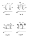
- FIG. 3A to FIG. 3B schematically illustrates a fabrication method of the trench power MOSFET structure according to a second embodiment of the present invention.
- the difference between the second embodiment and the first embodiment is shown in the FIG. 3A .
- FIG. 3A after the step of forming a gate polysilicon structure 340 , remove a gate dielectric layer 330 on the surface of a silicon substrate 310 and a portion of the gate dielectric layer 330 in a gate trench 320 . Then, as shown in FIG. 3B , a passivation layer 334 is formed on the gate polysilicon structure 340 and the silicon substrate 310 .
- the passivation layer 334 on the gate polysilicon structure 340 has sufficient thickness to prevent the impurities implanted into gate polysilicon structure 340 in the later step of forming the source doped region. In addition, it can also prevent impurities of the source doped region from diffusing into the gate polysilicon structure 340 through the sidewall of the gate trench 320 .
- FIG. 4A to FIG. 4B schematically illustrates a fabrication method of the trench power MOSFET structure according to a third embodiment of the present invention.
- the difference between the third embodiment and the first embodiment is in the thermal drive-in step for forming the source doped region.
- the thermal drive-in step in the instant embodiment is delayed and to be completed with the RTA step of forming the metal silicide.
- FIG. 4A after the formation of a body region 450 , the impurities of a second conductive type are implanted into the body region 450 to form a second conductive type doped region 461 .
- a portion of the gate dielectric layer and the passivation layer are removed and the upper surface of the gate polysilicon structure 440 is exposed.
- a dielectric spacer 433 is formed on the exposed sidewall of the gate trench.
- a metal layer 472 is deposited on the gate polysilicon structure 440 and the second conductive type doped region 461 .
- the RTA process is further applied to form a source doped region 460 ′ and a metal silicide layer 472 ′ simultaneously.
- the rest of the steps in the present embodiment are essentially the same as the steps described in the first embodiment, and further descriptions are hereby omitted.
Landscapes
- Engineering & Computer Science (AREA)
- Microelectronics & Electronic Packaging (AREA)
- Power Engineering (AREA)
- Physics & Mathematics (AREA)
- Ceramic Engineering (AREA)
- Condensed Matter Physics & Semiconductors (AREA)
- General Physics & Mathematics (AREA)
- Computer Hardware Design (AREA)
- Manufacturing & Machinery (AREA)
- Chemical & Material Sciences (AREA)
- Crystallography & Structural Chemistry (AREA)
- Electrodes Of Semiconductors (AREA)
Applications Claiming Priority (3)
| Application Number | Priority Date | Filing Date | Title |
|---|---|---|---|
| TW100112491A | 2011-04-11 | ||
| TW100112491A TWI469193B (zh) | 2011-04-11 | 2011-04-11 | 高密度溝槽式功率半導體結構與其製造方法 |
| TW100112491 | 2011-04-11 |
Publications (2)
| Publication Number | Publication Date |
|---|---|
| US20120256258A1 US20120256258A1 (en) | 2012-10-11 |
| US8900950B2 true US8900950B2 (en) | 2014-12-02 |
Family
ID=46965432
Family Applications (1)
| Application Number | Title | Priority Date | Filing Date |
|---|---|---|---|
| US13/425,365 Active 2032-10-09 US8900950B2 (en) | 2011-04-11 | 2012-03-20 | Trench power MOSFET structure with high cell density and fabrication method thereof |
Country Status (2)
| Country | Link |
|---|---|
| US (1) | US8900950B2 (zh) |
| TW (1) | TWI469193B (zh) |
Families Citing this family (6)
| Publication number | Priority date | Publication date | Assignee | Title |
|---|---|---|---|---|
| WO2012088447A1 (en) * | 2010-12-24 | 2012-06-28 | Marc Henness | Electrical circuit for controlling electrical power to drive an inductive load |
| CN102800704A (zh) * | 2012-08-29 | 2012-11-28 | 上海宏力半导体制造有限公司 | 沟槽式mos晶体管及其制造方法、集成电路 |
| CN109326621B (zh) * | 2018-10-17 | 2021-02-09 | 德淮半导体有限公司 | 形成图像传感器的方法及图像传感器 |
| CN112133750B (zh) * | 2019-06-25 | 2024-02-13 | 华润微电子(重庆)有限公司 | 深沟槽功率器件及其制备方法 |
| DE102020115157A1 (de) * | 2020-06-08 | 2021-12-09 | Fraunhofer-Gesellschaft zur Förderung der angewandten Forschung eingetragener Verein | Verfahren zur Herstellung eines Trench-MOSFET |
| CN113594042B (zh) * | 2021-07-28 | 2023-08-18 | 上海华虹宏力半导体制造有限公司 | Mosfet的制作方法 |
Citations (4)
| Publication number | Priority date | Publication date | Assignee | Title |
|---|---|---|---|---|
| US5027185A (en) * | 1988-06-06 | 1991-06-25 | Industrial Technology Research Institute | Polycide gate FET with salicide |
| US6489204B1 (en) * | 2001-08-20 | 2002-12-03 | Episil Technologies, Inc. | Save MOS device |
| US20030168695A1 (en) * | 2002-03-07 | 2003-09-11 | International Rectifier Corp. | Silicide gate process for trench MOSFET |
| US6841830B2 (en) * | 2002-12-31 | 2005-01-11 | Industrial Technology Research Institute | Metal oxide semiconductor field effect transistors (MOSFETS) used in ink-jet head chips and method for making the same |
Family Cites Families (1)
| Publication number | Priority date | Publication date | Assignee | Title |
|---|---|---|---|---|
| US7667264B2 (en) * | 2004-09-27 | 2010-02-23 | Alpha And Omega Semiconductor Limited | Shallow source MOSFET |
-
2011
- 2011-04-11 TW TW100112491A patent/TWI469193B/zh active
-
2012
- 2012-03-20 US US13/425,365 patent/US8900950B2/en active Active
Patent Citations (4)
| Publication number | Priority date | Publication date | Assignee | Title |
|---|---|---|---|---|
| US5027185A (en) * | 1988-06-06 | 1991-06-25 | Industrial Technology Research Institute | Polycide gate FET with salicide |
| US6489204B1 (en) * | 2001-08-20 | 2002-12-03 | Episil Technologies, Inc. | Save MOS device |
| US20030168695A1 (en) * | 2002-03-07 | 2003-09-11 | International Rectifier Corp. | Silicide gate process for trench MOSFET |
| US6841830B2 (en) * | 2002-12-31 | 2005-01-11 | Industrial Technology Research Institute | Metal oxide semiconductor field effect transistors (MOSFETS) used in ink-jet head chips and method for making the same |
Also Published As
| Publication number | Publication date |
|---|---|
| TWI469193B (zh) | 2015-01-11 |
| US20120256258A1 (en) | 2012-10-11 |
| TW201241882A (en) | 2012-10-16 |
Similar Documents
| Publication | Publication Date | Title |
|---|---|---|
| TWI458097B (zh) | 溝渠式閘極金氧半場效電晶體及其製造方法 | |
| US7816720B1 (en) | Trench MOSFET structure having improved avalanche capability using three masks process | |
| US8900950B2 (en) | Trench power MOSFET structure with high cell density and fabrication method thereof | |
| US8222108B2 (en) | Method of making a trench MOSFET having improved avalanche capability using three masks process | |
| US7217976B2 (en) | Low temperature process and structures for polycide power MOSFET with ultra-shallow source | |
| TW200534340A (en) | Method and apparatus for forming an SOI body-contacted transistor | |
| JP2004504711A (ja) | 高速トレンチ二重拡散金属酸化膜半導体 | |
| KR101332590B1 (ko) | 개선된 성능을 갖는 파워 반도체 장치 및 방법 | |
| US7824985B2 (en) | Method for manufacturing a recessed gate transistor | |
| US20130256786A1 (en) | Trench mosfet with shielded electrode and avalanche enhancement region | |
| US6734109B2 (en) | Method of building a CMOS structure on thin SOI with source/drain electrodes formed by in situ doped selective amorphous silicon | |
| CN110364483B (zh) | 半导体结构及其形成方法 | |
| CN207587740U (zh) | 晶体管及半导体器件 | |
| US20130164915A1 (en) | Method for fabricating power semiconductor device with super junction structure | |
| JP2007005575A (ja) | 半導体装置およびその製造方法 | |
| CN112117193A (zh) | 碳化硅mosfet器件及其制造方法 | |
| US20130299901A1 (en) | Trench mosfet structures using three masks process | |
| US8354315B2 (en) | Fabrication method of a power semicondutor structure with schottky diode | |
| CN112530867B (zh) | 沟槽型场效应晶体管结构及其制备方法 | |
| US20100244109A1 (en) | Trenched metal-oxide-semiconductor device and fabrication thereof | |
| US9214531B2 (en) | Trenched power MOSFET with enhanced breakdown voltage and fabrication method thereof | |
| CN109087939B (zh) | 半导体结构的形成方法、ldmos晶体管及其形成方法 | |
| CN112951765A (zh) | 半导体结构及其形成方法 | |
| CN216389378U (zh) | 一种沟槽型功率器件 | |
| CN220774378U (zh) | 金属氧化物半导体mos晶体管和设备 |
Legal Events
| Date | Code | Title | Description |
|---|---|---|---|
| AS | Assignment |
Owner name: GREAT POWER SEMICONDUCTOR CORP., TAIWAN Free format text: ASSIGNMENT OF ASSIGNORS INTEREST;ASSIGNOR:HSU, HSIU-WEN;REEL/FRAME:027897/0161 Effective date: 20120315 |
|
| STCF | Information on status: patent grant |
Free format text: PATENTED CASE |
|
| AS | Assignment |
Owner name: SUPER GROUP SEMICONDUCTOR CO., LTD., TAIWAN Free format text: ASSIGNMENT OF ASSIGNORS INTEREST;ASSIGNOR:GREAT POWER SEMICONDUCTOR CORP.;REEL/FRAME:041866/0090 Effective date: 20170327 |
|
| MAFP | Maintenance fee payment |
Free format text: PAYMENT OF MAINTENANCE FEE, 4TH YR, SMALL ENTITY (ORIGINAL EVENT CODE: M2551) Year of fee payment: 4 |
|
| MAFP | Maintenance fee payment |
Free format text: PAYMENT OF MAINTENANCE FEE, 8TH YR, SMALL ENTITY (ORIGINAL EVENT CODE: M2552); ENTITY STATUS OF PATENT OWNER: SMALL ENTITY Year of fee payment: 8 |