US8884721B2 - Laminated LC filter - Google Patents
Laminated LC filter Download PDFInfo
- Publication number
- US8884721B2 US8884721B2 US13/290,179 US201113290179A US8884721B2 US 8884721 B2 US8884721 B2 US 8884721B2 US 201113290179 A US201113290179 A US 201113290179A US 8884721 B2 US8884721 B2 US 8884721B2
- Authority
- US
- United States
- Prior art keywords
- inductor
- laminated
- filter
- electrode
- electrode layer
- Prior art date
- Legal status (The legal status is an assumption and is not a legal conclusion. Google has not performed a legal analysis and makes no representation as to the accuracy of the status listed.)
- Active, expires
Links
Images


Classifications
-
- H—ELECTRICITY
- H03—ELECTRONIC CIRCUITRY
- H03H—IMPEDANCE NETWORKS, e.g. RESONANT CIRCUITS; RESONATORS
- H03H7/00—Multiple-port networks comprising only passive electrical elements as network components
- H03H7/01—Frequency selective two-port networks
- H03H7/09—Filters comprising mutual inductance
-
- H—ELECTRICITY
- H03—ELECTRONIC CIRCUITRY
- H03H—IMPEDANCE NETWORKS, e.g. RESONANT CIRCUITS; RESONATORS
- H03H7/00—Multiple-port networks comprising only passive electrical elements as network components
- H03H7/01—Frequency selective two-port networks
- H03H7/17—Structural details of sub-circuits of frequency selective networks
- H03H7/1741—Comprising typical LC combinations, irrespective of presence and location of additional resistors
- H03H7/1775—Parallel LC in shunt or branch path
-
- H—ELECTRICITY
- H03—ELECTRONIC CIRCUITRY
- H03H—IMPEDANCE NETWORKS, e.g. RESONANT CIRCUITS; RESONATORS
- H03H1/00—Constructional details of impedance networks whose electrical mode of operation is not specified or applicable to more than one type of network
- H03H2001/0021—Constructional details
- H03H2001/0057—Constructional details comprising magnetic material
-
- H—ELECTRICITY
- H03—ELECTRONIC CIRCUITRY
- H03H—IMPEDANCE NETWORKS, e.g. RESONANT CIRCUITS; RESONATORS
- H03H1/00—Constructional details of impedance networks whose electrical mode of operation is not specified or applicable to more than one type of network
- H03H2001/0021—Constructional details
- H03H2001/0085—Multilayer, e.g. LTCC, HTCC, green sheets
Definitions
- the present invention relates to a laminated LC filter preferably for use in an electronic device or other suitable device, for example.
- An existing laminated LC filter is composed of a laminate in which a dielectric layer and an electrode layer are laminated; and a plurality of LC resonators provided in the laminate.
- an LC filter 100 disclosed in Japanese Unexamined Patent Application Publication No. 10-190391 as shown in FIG. 9 is known.
- the LC filter 100 includes inductor portions 92 and 93 in which coils 86 and 87 are included, respectively.
- Each of the coils 86 and 87 is formed by laminating sheets in which coil conductors and via electrodes for defining a relay are provided, and their axial directions are perpendicular to input/output external electrodes 95 and 96 .
- a ground electrode 90 and an electrode 91 are disposed in a capacitor portion 94 so as to face each other.
- An end of the coil 86 is electrically connected to an end 91 a of the electrode 91 via a connection electrode 99 provided on a side surface of the filter 100 on the near side.
- An end of the coil 87 is electrically connected to the other end 91 b of the electrode 91 via a connection electrode 80 provided on a side surface of the filter 100 on the far side.
- the directions of magnetic fields of the coils 86 and 87 are parallel to a board on which the LC filter is mounted.
- radiation of magnetic flux influences an adjacent electronic component.
- the coil conductors are mainly formed of pattern printing electrodes, and hence an inductance with a great Q value is not obtained.
- the insertion loss of the filter increases.
- preferred embodiments of the present invention provide an LC filter in which the direction of a magnetic field is perpendicular to a board on which the LC filter is mounted, thereby reducing the influence of radiation of magnetic flux on an adjacent electronic component, and in which an inductance with a great Q value is obtained to provide low loss.
- a laminated LC filter includes a laminate including a plurality of dielectric layers, a capacitor electrode layer, an inductor electrode layer, a ground electrode layer, an input/output electrode layer, and a via electrode extending through the dielectric layers in a thickness direction thereof, and having a substantially rectangular parallelepiped shape; and an LC resonator that includes a capacitor including the capacitor electrode layer and an inductor including the inductor electrode layer.
- the inductor includes the inductor electrode layer and the via electrode extending through the plurality of dielectric layers in the thickness direction, and preferably has a substantially loop shape.
- the capacitor preferably includes the ground electrode layer and the capacitor electrode layer located so as to face the ground electrode layer.
- the input/output electrode layer is located on an outermost surface that faces in a lamination direction of the laminate.
- the loop-shaped inductor has a structure such that the via electrode is a principal body.
- an inductor with a great Q value can be obtained, and as a result, it is possible to reduce the insertion loss of the filter.
- a magnetic layer is located on a surface perpendicular to a direction of a magnetic field of the inductor among surfaces of the laminate.
- the inductance of the inductor of the laminated LC filter can be increased.
- the magnetic layer prevents spreading of the magnetic field of the inductor, and in a device in which the laminated LC filter is mounted, influence of the magnetic field on an adjacent electronic component can be reduced.
- the magnetic layer has an effect of mechanically reinforcing the laminated LC filter, due to its rigidity, and thus strength against inter-layer separation of the laminate and cracking caused by bending or the like can be increased.
- a magnetic layer is arranged so as to extend through a loop surface of the loop-shaped inductor.
- the inductance of the inductor of the laminated LC filter can be increased.
- the magnetic layer prevents spreading of the magnetic field of the inductor, and in a device in which the laminated LC filter is mounted, influence of the magnetic field on an adjacent electronic component can be reduced.
- the LC resonator includes two or more LC resonators of which adjacent LC resonators are coupled to each other, and a magnetic layer is provided between the loop-shaped inductors of the adjacent LC resonators.
- the magnetic layer due to an effect of the magnetic layer preventing spreading of magnetic flux, the magnetic layer has an effect of weakening electromagnetic coupling between the inductors and can be used to adjust the electromagnetic coupling therebetween.
- a surface parallel to the lamination direction among surfaces of the laminate is a bottom surface.
- the magnetic field of the loop-shaped inductor is directed so as to be radiated from the center of the loop, and its direction is perpendicular to a board on which the laminated LC filter is mounted.
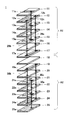
- FIG. 1 is an exploded perspective view of a laminate of a laminated LC filter according to a first preferred embodiment of the present invention.
- FIGS. 2A and 2B are external perspective views of the laminated LC filter in FIG. 1 .
- FIG. 3 is an equivalent circuit diagram of the laminated LC filter in FIG. 1 .
- FIG. 4 is an exploded perspective view of a modified example of the laminated LC filter in FIG. 1 .
- FIG. 5 is an exploded perspective view of a laminate of a laminated LC filter according to a second preferred embodiment of the present invention.
- FIGS. 6A to 6C are external perspective views of the laminated LC filter in FIG. 5 .
- FIGS. 7A to 7C are diagrams illustrating a laminated LC filter according to a third preferred embodiment of the present invention.
- FIGS. 8A and 8B are diagrams illustrating a laminated LC filter according to a fourth preferred embodiment of the present invention.
- FIG. 9 is a diagram illustrating an existing laminated LC filter.
- FIG. 1 is an exploded perspective view of a laminated LC filter 1 of the first preferred embodiment.
- FIG. 2A is an external perspective view of the laminated LC filter 1 in FIG. 1
- FIG. 2B is an external perspective view of the laminated LC filter in a state where a board (not shown) on which the laminated LC filter is mounted is located on the lower side.
- conductive films exposed to the outside are hatched.
- a plurality of dielectric layers and electrode layers are laminated, and via electrodes extend through the dielectric layers.
- ground electrodes are located on surfaces (hatched portions) thereof on the near side in FIG. 1 and surfaces opposed to these surfaces.
- the ground electrodes on the surfaces on the near side define an electrode 31 a in FIGS. 2A and 2B .
- the dielectric layers 11 - 25 are produced, for example, preferably by applying a slurry of a ceramic dielectric material containing alumina and glass as principal components, onto a film by a doctor blade method.
- the electrode layers 11 a - 15 a , 17 a , 19 a , and 21 a - 25 a are formed, for example, preferably by applying a photosensitive conductive paste onto the dielectric layers by a spin coat method or the like and using a photolithographic method. Alternatively, these layers may be formed by screen printing a conductive paste directly onto the dielectric layers.
- the laminated LC filter 1 specifically, the configurations of the laminated dielectric layers and the electrode layer and the via electrodes formed in each dielectric layer will be described in detail.
- the laminated LC filter 1 preferably includes two LC resonators having the same configurations and coupled to each other.
- the layers from the uppermost dielectric layer 11 to the dielectric layer 17 constitute a first block A 1
- the layers from the dielectric layer 18 to the lowermost dielectric layer 25 constitute a second block A 2 .
- the input/output electrode 11 a and a portion of a via electrode 29 a are provided and connected to each other.
- the ground electrodes 12 a and 12 b , the inductor electrode 12 c , and portions of the via electrodes 29 a , 29 b , and 29 c are provided.
- the ground electrode 12 a is connected to the external ground electrodes 31 a and 31 b
- the ground electrode 12 b is connected to the via electrode 29 c and the external ground electrode 31 b
- the inductor electrode 12 c is connected to the via electrodes 29 a and 29 b.
- the capacitor electrode 13 a and portions of the via electrodes 29 a , 29 b , and 29 c are provided in the dielectric layer 13 .
- the capacitor electrode 13 a is connected to the via electrode 29 a.
- the ground electrode 14 a and portions of the via electrodes 29 a , 29 b , and 29 c are provided in the dielectric layer 14 .
- the ground electrode 14 a is connected to the external ground electrodes 31 a and 31 b.
- the capacitor electrode 15 a and portions of the via electrodes 29 a , 29 b , and 29 c are provided in the dielectric layer 15 .
- the capacitor electrode 15 a is connected to the via electrode 29 a.
- portions of the via electrodes 29 b and 29 c are provided.
- the inductor electrode 17 a and portions of the via electrodes 29 b and 29 c are provided in the dielectric layer 17 .
- the inductor electrode 17 a is connected to the via electrodes 29 b and 29 c.
- the ground electrode 12 a , the capacitor electrode 13 a , the ground electrode 14 a , and the capacitor electrode 15 a are laminated on the dielectric layers 12 to 15 in order from above.
- the two capacitor electrodes 13 a and 15 a are connected to each other via the via electrode 29 a to constitute a first capacitor.
- a first inductor preferably includes a substantially loop-shaped line that extends from a connection point between the inductor electrode layer 12 c and the via electrode 29 a through the inductor electrode layer 12 c , the via electrode 29 b , the inductor electrode layer 17 a , and the via electrode 29 c in order, to a connection point between the via electrode 29 c and the ground electrode layer 12 b .
- the via electrodes when seen in an arrangement in which the laminated LC filter is mounted on a mounting board, the via electrodes extend sequentially through the dielectric layers in parallel to the mounting surface to define the inductor.
- dielectric layers 19 - 25 , and electrode layers 19 and 21 a - 25 a are laminated so as to be symmetrical to the first block A 1 with respect to the dielectric layer 18 , and via electrodes 30 a , 30 b , and 30 c are formed, to constitute a second capacitor and an inductor.
- the lowermost layer 25 is disposed in an orientation in which the uppermost layer 11 of the first block A 1 is reversed.
- a third capacitor preferably includes the inductor electrode layers 17 a and 19 a.
- FIG. 3 is an equivalent circuit diagram of the laminated LC filter 1 .
- a capacitor C 1 corresponds to the first capacitor
- an inductor L 1 corresponds to the first inductor.
- the first capacitor C 1 and the first inductor L 1 constitute a first LC resonator 41 .
- a capacitor C 2 and an inductor L 2 correspond to the second capacitor and a second inductor, respectively, and constitute a second LC resonator 42 .
- a capacitor C 3 corresponds to the third capacitor.
- the first LC resonator 41 and the second LC resonator 42 are electromagnetically coupled to each other via the first inductor L 1 and the second inductor L 2 .
- the first and second inductors When the laminated LC filter 1 comes into an operating state, the first and second inductors generate magnetic fields in directions perpendicular to the loop surfaces thereof.
- the directions of the magnetic fields are perpendicular to a lamination direction of the laminate, and are the right-left direction in FIGS. 1 and 2A and the up-down direction in FIG. 2B .
- the directions of the magnetic fields of the first and second inductors of the laminated LC filter 1 in the present preferred embodiment are perpendicular to the board on which the LC filter is mounted, and hence influence of radiation of magnetic flux on an adjacently mounted electronic component can be prevented.
- the first inductor includes, as a portion of the line, the via electrodes 29 b and 29 c extending through a plurality of the dielectric layers in the thickness direction thereof, and preferably has a substantially loop shape.
- the cross section is easily made larger than the thickness of a pattern printing electrode, and no edge corner is formed as in a pattern printing electrode.
- the resistance value of the via electrode can be decreased. Therefore, an inductor with a great Q value can be obtained, and it is possible to prevent the insertion loss of the laminated LC filter 1 .
- the increase is possible by increasing the number of the dielectric layer 16 or 20 in FIG. 1 to lengthen the via electrodes and make the loop shape of the inductor large in size. This increase can be made without deteriorating the Q value of the inductor.
- the loop of each inductor preferably has a single-winding structure, but may have a double-winding structure as in a laminated LC filter 1 a shown in FIG. 4 .
- dielectric layers 111 - 125 dielectric layers 111 - 125 , and electrode layers 111 a - 116 a and 121 a - 125 a are laminated, and via electrodes 129 a - 129 e and 130 a - 130 e are provided.
- the basic manufacturing method and structure of the laminated LC filter 1 a and the configurations of capacitors are the same as those in the laminated LC filter 1 .
- a first inductor of a first block A 101 preferably includes a substantially loop-shaped line that extends from a connection point between the inductor electrode layer 112 c and the via electrode 129 a through the inductor electrode layer 112 c , the via electrode 129 b , the inductor electrode layer 117 a , the via electrode 129 c , the inductor electrode 116 a , the via electrode 129 e , the inductor electrode layer 117 b , and the via electrode 129 d in order, to a connection point between the via electrode 129 d and the ground electrode layer 116 b.
- a second inductor of a second block A 102 is arranged so as to be symmetrical to the first inductor of the first block A 101 .
- a third capacitor preferably includes the facing inductor electrode layers 117 a and 119 a and the facing inductor electrode layers 117 b and 119 b.
- the number of winding of each inductor can be changed to adjust the inductance.
- the number of winding of the inductor can be increased further by the arrangement of the electrode layers such as the dielectric layers 116 , 116 A, and 117 and the via electrodes.
- FIG. 5 is an exploded perspective view of the laminated LC filter 2
- FIG. 6A is an external view of the laminated LC filter 2
- FIG. 6B is an external perspective view of the laminated LC filter 2 in a state where the laminated LC filter is mounted on a mounting board (not shown) such that the board is located on the lower side.
- FIG. 6C is a schematic diagram schematically illustrating a direction in which the magnetic layer 51 and dielectric layers 11 to 25 are laminated, wherein the mounting board is similarly located on the lower side.
- the magnetic layer 51 is provided on a surface parallel to the loop surfaces of the first and second inductors of the laminated LC filter 1 .
- the magnetic fields of the inductors are perpendicular to the loop surfaces.
- the magnetic layer 51 is present in an area through which the magnetic fields of the first and second inductors pass, and the inductances of these inductors can be increased.
- the magnetic layer 51 has an effect of preventing spreading of the magnetic field.
- the magnetic layer 51 can reduce influence of radiation of magnetic flux on an adjacent electronic component. Meanwhile, due to the effect of preventing spreading of the magnetic flux, coupling of the inductors electromagnetically coupled to each other is made loose, and the electromagnetic coupling between the first inductor L 1 and the second inductor L 2 is weakened.
- the laminated LC filter 2 receives a bending force in the up-down direction in FIG. 6C .
- This direction is parallel to the laminated surface of the laminate, and thus there is a high risk that inter-layer separation and a crack will occur due to bending.
- the added magnetic layer 51 is perpendicular to the laminated surface and thus has an effect of preventing inter-layer separation and a crack from occurring.
- a laminated LC filter 3 is obtained by boring the body of the laminate from the surface 32 side so as to perpendicularly extend through the loop surfaces of the first and second inductors in the laminated LC filter 1 of the first preferred embodiment, and putting a magnetic material therein to form magnetic layers 56 .
- FIG. 7A is an external perspective view of the laminated LC filter 3
- FIG. 7B is an image diagram illustrating a state where the line of the first inductor is a loop 55 a , the line of the second inductor is a loop 55 b , and the magnetic layers 56 perpendicularly extend through the loop surfaces of these loops.
- the magnetic layers 56 are located in areas through which the magnetic fields of the first and second inductors pass, and thus the inductances of these inductors can be increased. In addition, due to the effect of preventing spreading of magnetic flux, the magnetic layers 56 can reduce influence of radiation of magnetic flux on an adjacent electronic component. Meanwhile, as described above, when spreading of magnetic flux is prevented, there is also an influence that electromagnetic coupling between the first inductor L 1 and the second inductor L 2 is weakened.
- a laminated LC filter 4 is obtained preferably by forming the magnetic layer 51 of the second preferred embodiment on the surface 32 in the laminated LC filter 3 .
- FIG. 7C is an external perspective view of the laminated LC filter 4 .
- the magnetic layers 56 are shown preferably having a substantially cylindrical shape, but their shapes may be substantially rectangular parallelepipeds or substantially polyhedrons and their sizes are not limited as long as they are located within the loops forming the inductors.
- a laminated LC filter 5 is obtained preferably by boring the body of the laminate in the laminated LC filter 1 of the first preferred embodiment so as to extend from the surface 32 between the first and second inductors, and putting a magnetic material therein to form a magnetic layer 58 .
- FIG. 8A is an external perspective view of the laminated LC filter 5
- FIG. 8B is an image diagram illustrating a state where the magnetic layer 58 is provided between the first inductor loop 55 a and the second inductor loop 55 b.
- the magnetic layer 58 Due to the effect of preventing spreading of magnetic flux as described above, the magnetic layer 58 has an effect of weakening the electromagnetic coupling between the first inductor L 1 and the second inductor L 2 and can be used to adjust the electromagnetic coupling therebetween.
- the laminated LC filter 5 it is possible to use both or at least one of the magnetic layer 51 shown in the second preferred embodiment and the magnetic layers 56 shown in the third preferred embodiment. In this case, the effects of each layer can be obtained.
- the magnetic layer 58 is shown as preferably having a substantially cylindrical shape, but its shape may be a substantially rectangular parallelepiped or a substantially polyhedron and its size is not limited as long as it is located between the loops defining the inductors.
Landscapes
- Filters And Equalizers (AREA)
- Coils Or Transformers For Communication (AREA)
Applications Claiming Priority (2)
| Application Number | Priority Date | Filing Date | Title |
|---|---|---|---|
| JP2010251291A JP5387542B2 (ja) | 2010-11-09 | 2010-11-09 | 積層型lcフィルタ |
| JP2010-251291 | 2010-11-09 |
Publications (2)
| Publication Number | Publication Date |
|---|---|
| US20120112856A1 US20120112856A1 (en) | 2012-05-10 |
| US8884721B2 true US8884721B2 (en) | 2014-11-11 |
Family
ID=46019070
Family Applications (1)
| Application Number | Title | Priority Date | Filing Date |
|---|---|---|---|
| US13/290,179 Active 2032-11-17 US8884721B2 (en) | 2010-11-09 | 2011-11-07 | Laminated LC filter |
Country Status (2)
| Country | Link |
|---|---|
| US (1) | US8884721B2 (ja) |
| JP (1) | JP5387542B2 (ja) |
Cited By (1)
| Publication number | Priority date | Publication date | Assignee | Title |
|---|---|---|---|---|
| US20140247192A1 (en) * | 2012-02-01 | 2014-09-04 | Murata Manufacturing Co., Ltd. | Wireless communication module and communication terminal apparatus incorporating the same |
Families Citing this family (5)
| Publication number | Priority date | Publication date | Assignee | Title |
|---|---|---|---|---|
| JP6624026B2 (ja) * | 2016-05-20 | 2019-12-25 | 株式会社村田製作所 | 積層型電子部品 |
| TWI643454B (zh) * | 2016-10-05 | 2018-12-01 | 日商村田製作所股份有限公司 | Multilayer LC filter |
| TWI656731B (zh) * | 2016-12-04 | 2019-04-11 | 日商村田製作所股份有限公司 | Multilayer LC filter |
| CN109887708B (zh) * | 2017-11-29 | 2021-04-09 | 株式会社村田制作所 | 电子部件 |
| JP7115235B2 (ja) * | 2018-11-08 | 2022-08-09 | 株式会社村田製作所 | 電子部品及び電子部品の製造方法 |
Citations (8)
| Publication number | Priority date | Publication date | Assignee | Title |
|---|---|---|---|---|
| JPH03274814A (ja) | 1990-03-23 | 1991-12-05 | Toko Inc | 積層型共振子とそれを用いたフィルタ |
| JPH0935936A (ja) | 1995-07-19 | 1997-02-07 | Murata Mfg Co Ltd | インダクタ内蔵電子部品 |
| JPH10190391A (ja) | 1996-12-27 | 1998-07-21 | Murata Mfg Co Ltd | 積層型lcフィルタ |
| JPH1126241A (ja) | 1996-11-21 | 1999-01-29 | Tdk Corp | 積層型電子部品とその製造方法 |
| JP2002252117A (ja) | 2000-12-19 | 2002-09-06 | Murata Mfg Co Ltd | 積層型コイル部品及びその製造方法 |
| JP2005340586A (ja) | 2004-05-28 | 2005-12-08 | Murata Mfg Co Ltd | 積層型電子部品 |
| JP2009246889A (ja) | 2008-03-31 | 2009-10-22 | Tdk Corp | 積層型電子部品 |
| US20090309683A1 (en) * | 2008-06-16 | 2009-12-17 | Cochran William T | Sensor inductors, sensors for monitoring movements and positioning, apparatus, systems and methods therefore |
-
2010
- 2010-11-09 JP JP2010251291A patent/JP5387542B2/ja not_active Expired - Fee Related
-
2011
- 2011-11-07 US US13/290,179 patent/US8884721B2/en active Active
Patent Citations (10)
| Publication number | Priority date | Publication date | Assignee | Title |
|---|---|---|---|---|
| JPH03274814A (ja) | 1990-03-23 | 1991-12-05 | Toko Inc | 積層型共振子とそれを用いたフィルタ |
| JPH0935936A (ja) | 1995-07-19 | 1997-02-07 | Murata Mfg Co Ltd | インダクタ内蔵電子部品 |
| US6222427B1 (en) | 1995-07-19 | 2001-04-24 | Murata Manufacturing Co., Ltd. | Inductor built-in electronic parts using via holes |
| JPH1126241A (ja) | 1996-11-21 | 1999-01-29 | Tdk Corp | 積層型電子部品とその製造方法 |
| US6147573A (en) * | 1996-11-21 | 2000-11-14 | Tdk Corporation | Multilayer electronic part with planar terminal electrodes |
| JPH10190391A (ja) | 1996-12-27 | 1998-07-21 | Murata Mfg Co Ltd | 積層型lcフィルタ |
| JP2002252117A (ja) | 2000-12-19 | 2002-09-06 | Murata Mfg Co Ltd | 積層型コイル部品及びその製造方法 |
| JP2005340586A (ja) | 2004-05-28 | 2005-12-08 | Murata Mfg Co Ltd | 積層型電子部品 |
| JP2009246889A (ja) | 2008-03-31 | 2009-10-22 | Tdk Corp | 積層型電子部品 |
| US20090309683A1 (en) * | 2008-06-16 | 2009-12-17 | Cochran William T | Sensor inductors, sensors for monitoring movements and positioning, apparatus, systems and methods therefore |
Non-Patent Citations (2)
| Title |
|---|
| Machine translation of JP 11-026241, translated May 29, 2014. * |
| Official Communication issued in corresponding Japanese Patent Application No. 2010-251291, mailed on Dec. 11, 2012. |
Cited By (4)
| Publication number | Priority date | Publication date | Assignee | Title |
|---|---|---|---|---|
| US20140247192A1 (en) * | 2012-02-01 | 2014-09-04 | Murata Manufacturing Co., Ltd. | Wireless communication module and communication terminal apparatus incorporating the same |
| US9496597B2 (en) * | 2012-02-01 | 2016-11-15 | Murata Manufacturing Co., Ltd. | Wireless communication module and communication terminal apparatus incorporating the same |
| US20170033444A1 (en) * | 2012-02-01 | 2017-02-02 | Murata Manufacturing Co., Ltd. | Wireless communication module and communication terminal apparatus incorporating the same |
| US9793600B2 (en) * | 2012-02-01 | 2017-10-17 | Murata Manufacturing Co., Ltd. | Wireless communication module and communication terminal apparatus incorporating the same |
Also Published As
| Publication number | Publication date |
|---|---|
| JP2012105026A (ja) | 2012-05-31 |
| US20120112856A1 (en) | 2012-05-10 |
| JP5387542B2 (ja) | 2014-01-15 |
Similar Documents
| Publication | Publication Date | Title |
|---|---|---|
| US8884721B2 (en) | Laminated LC filter | |
| JP3127792B2 (ja) | Lc共振器およびlcフィルタ | |
| JP5787760B2 (ja) | フィルタ | |
| KR101862401B1 (ko) | 적층형 인덕터 및 그 제조방법 | |
| US7453344B2 (en) | Multilayer coil component | |
| JP4983881B2 (ja) | 積層帯域通過フィルタ | |
| WO2013058144A1 (ja) | 複合電子部品 | |
| JP6801826B2 (ja) | フィルタ素子 | |
| US8289104B2 (en) | Electronic component | |
| US9479136B2 (en) | Electronic component | |
| US8169288B2 (en) | Electronic component and method for making the same | |
| US20060022770A1 (en) | Lamination type electronic component | |
| JP7322934B2 (ja) | コイル部品および、これを含むフィルタ回路 | |
| US8878632B2 (en) | Laminated filter | |
| KR20160032581A (ko) | 인덕터 어레이 칩 및 그 실장기판 | |
| JP2007259026A (ja) | 積層型ノイズフィルタ | |
| EP1564761A1 (en) | Laminated coil component and method of producing the same | |
| JP2005150168A (ja) | 積層コイル部品 | |
| CN215342186U (zh) | 线圈部件以及包括其的滤波器电路 | |
| US9634633B2 (en) | Electronic component | |
| JP2008271204A (ja) | 積層型電子部品 | |
| JPH0669038A (ja) | チップ型コイル | |
| JP2003217935A (ja) | 積層インダクタアレイ | |
| JP2000260621A (ja) | 積層型コモンモードチョークコイル | |
| JP2002305123A (ja) | 積層セラミック電子部品の製造方法及び積層インダクタの製造方法 |
Legal Events
| Date | Code | Title | Description |
|---|---|---|---|
| AS | Assignment |
Owner name: MURATA MANUFACTURING CO., LTD., JAPAN Free format text: ASSIGNMENT OF ASSIGNORS INTEREST;ASSIGNOR:MIZOGUCHI, NAOKI;REEL/FRAME:027182/0572 Effective date: 20111103 |
|
| STCF | Information on status: patent grant |
Free format text: PATENTED CASE |
|
| FEPP | Fee payment procedure |
Free format text: PAYOR NUMBER ASSIGNED (ORIGINAL EVENT CODE: ASPN); ENTITY STATUS OF PATENT OWNER: LARGE ENTITY |
|
| FEPP | Fee payment procedure |
Free format text: PAYER NUMBER DE-ASSIGNED (ORIGINAL EVENT CODE: RMPN); ENTITY STATUS OF PATENT OWNER: LARGE ENTITY Free format text: PAYOR NUMBER ASSIGNED (ORIGINAL EVENT CODE: ASPN); ENTITY STATUS OF PATENT OWNER: LARGE ENTITY |
|
| MAFP | Maintenance fee payment |
Free format text: PAYMENT OF MAINTENANCE FEE, 4TH YEAR, LARGE ENTITY (ORIGINAL EVENT CODE: M1551) Year of fee payment: 4 |
|
| MAFP | Maintenance fee payment |
Free format text: PAYMENT OF MAINTENANCE FEE, 8TH YEAR, LARGE ENTITY (ORIGINAL EVENT CODE: M1552); ENTITY STATUS OF PATENT OWNER: LARGE ENTITY Year of fee payment: 8 |