US8884721B2 - Laminated LC filter - Google Patents

Laminated LC filter Download PDF

Info

Publication number
US8884721B2
US8884721B2 US13/290,179 US201113290179A US8884721B2 US 8884721 B2 US8884721 B2 US 8884721B2 US 201113290179 A US201113290179 A US 201113290179A US 8884721 B2 US8884721 B2 US 8884721B2
Authority
US
United States
Prior art keywords
inductor
laminated
filter
electrode
electrode layer
Prior art date
Legal status (The legal status is an assumption and is not a legal conclusion. Google has not performed a legal analysis and makes no representation as to the accuracy of the status listed.)
Active, expires
Application number
US13/290,179
Other versions
US20120112856A1 (en
Inventor
Naoki Mizoguchi
Current Assignee (The listed assignees may be inaccurate. Google has not performed a legal analysis and makes no representation or warranty as to the accuracy of the list.)
Murata Manufacturing Co Ltd
Original Assignee
Murata Manufacturing Co Ltd
Priority date (The priority date is an assumption and is not a legal conclusion. Google has not performed a legal analysis and makes no representation as to the accuracy of the date listed.)
Filing date
Publication date
Application filed by Murata Manufacturing Co Ltd filed Critical Murata Manufacturing Co Ltd
Assigned to MURATA MANUFACTURING CO., LTD. reassignment MURATA MANUFACTURING CO., LTD. ASSIGNMENT OF ASSIGNORS INTEREST (SEE DOCUMENT FOR DETAILS). Assignors: MIZOGUCHI, NAOKI
Publication of US20120112856A1 publication Critical patent/US20120112856A1/en
Application granted granted Critical
Publication of US8884721B2 publication Critical patent/US8884721B2/en
Active legal-status Critical Current
Adjusted expiration legal-status Critical

Links

Images

Classifications

    • HELECTRICITY
    • H03ELECTRONIC CIRCUITRY
    • H03HIMPEDANCE NETWORKS, e.g. RESONANT CIRCUITS; RESONATORS
    • H03H7/00Multiple-port networks comprising only passive electrical elements as network components
    • H03H7/01Frequency selective two-port networks
    • H03H7/09Filters comprising mutual inductance
    • HELECTRICITY
    • H03ELECTRONIC CIRCUITRY
    • H03HIMPEDANCE NETWORKS, e.g. RESONANT CIRCUITS; RESONATORS
    • H03H7/00Multiple-port networks comprising only passive electrical elements as network components
    • H03H7/01Frequency selective two-port networks
    • H03H7/17Structural details of sub-circuits of frequency selective networks
    • H03H7/1741Comprising typical LC combinations, irrespective of presence and location of additional resistors
    • H03H7/1775Parallel LC in shunt or branch path
    • HELECTRICITY
    • H03ELECTRONIC CIRCUITRY
    • H03HIMPEDANCE NETWORKS, e.g. RESONANT CIRCUITS; RESONATORS
    • H03H1/00Constructional details of impedance networks whose electrical mode of operation is not specified or applicable to more than one type of network
    • H03H2001/0021Constructional details
    • H03H2001/0057Constructional details comprising magnetic material
    • HELECTRICITY
    • H03ELECTRONIC CIRCUITRY
    • H03HIMPEDANCE NETWORKS, e.g. RESONANT CIRCUITS; RESONATORS
    • H03H1/00Constructional details of impedance networks whose electrical mode of operation is not specified or applicable to more than one type of network
    • H03H2001/0021Constructional details
    • H03H2001/0085Multilayer, e.g. LTCC, HTCC, green sheets

Definitions

  • the present invention relates to a laminated LC filter preferably for use in an electronic device or other suitable device, for example.
  • An existing laminated LC filter is composed of a laminate in which a dielectric layer and an electrode layer are laminated; and a plurality of LC resonators provided in the laminate.
  • an LC filter 100 disclosed in Japanese Unexamined Patent Application Publication No. 10-190391 as shown in FIG. 9 is known.
  • the LC filter 100 includes inductor portions 92 and 93 in which coils 86 and 87 are included, respectively.
  • Each of the coils 86 and 87 is formed by laminating sheets in which coil conductors and via electrodes for defining a relay are provided, and their axial directions are perpendicular to input/output external electrodes 95 and 96 .
  • a ground electrode 90 and an electrode 91 are disposed in a capacitor portion 94 so as to face each other.
  • An end of the coil 86 is electrically connected to an end 91 a of the electrode 91 via a connection electrode 99 provided on a side surface of the filter 100 on the near side.
  • An end of the coil 87 is electrically connected to the other end 91 b of the electrode 91 via a connection electrode 80 provided on a side surface of the filter 100 on the far side.
  • the directions of magnetic fields of the coils 86 and 87 are parallel to a board on which the LC filter is mounted.
  • radiation of magnetic flux influences an adjacent electronic component.
  • the coil conductors are mainly formed of pattern printing electrodes, and hence an inductance with a great Q value is not obtained.
  • the insertion loss of the filter increases.
  • preferred embodiments of the present invention provide an LC filter in which the direction of a magnetic field is perpendicular to a board on which the LC filter is mounted, thereby reducing the influence of radiation of magnetic flux on an adjacent electronic component, and in which an inductance with a great Q value is obtained to provide low loss.
  • a laminated LC filter includes a laminate including a plurality of dielectric layers, a capacitor electrode layer, an inductor electrode layer, a ground electrode layer, an input/output electrode layer, and a via electrode extending through the dielectric layers in a thickness direction thereof, and having a substantially rectangular parallelepiped shape; and an LC resonator that includes a capacitor including the capacitor electrode layer and an inductor including the inductor electrode layer.
  • the inductor includes the inductor electrode layer and the via electrode extending through the plurality of dielectric layers in the thickness direction, and preferably has a substantially loop shape.
  • the capacitor preferably includes the ground electrode layer and the capacitor electrode layer located so as to face the ground electrode layer.
  • the input/output electrode layer is located on an outermost surface that faces in a lamination direction of the laminate.
  • the loop-shaped inductor has a structure such that the via electrode is a principal body.
  • an inductor with a great Q value can be obtained, and as a result, it is possible to reduce the insertion loss of the filter.
  • a magnetic layer is located on a surface perpendicular to a direction of a magnetic field of the inductor among surfaces of the laminate.
  • the inductance of the inductor of the laminated LC filter can be increased.
  • the magnetic layer prevents spreading of the magnetic field of the inductor, and in a device in which the laminated LC filter is mounted, influence of the magnetic field on an adjacent electronic component can be reduced.
  • the magnetic layer has an effect of mechanically reinforcing the laminated LC filter, due to its rigidity, and thus strength against inter-layer separation of the laminate and cracking caused by bending or the like can be increased.
  • a magnetic layer is arranged so as to extend through a loop surface of the loop-shaped inductor.
  • the inductance of the inductor of the laminated LC filter can be increased.
  • the magnetic layer prevents spreading of the magnetic field of the inductor, and in a device in which the laminated LC filter is mounted, influence of the magnetic field on an adjacent electronic component can be reduced.
  • the LC resonator includes two or more LC resonators of which adjacent LC resonators are coupled to each other, and a magnetic layer is provided between the loop-shaped inductors of the adjacent LC resonators.
  • the magnetic layer due to an effect of the magnetic layer preventing spreading of magnetic flux, the magnetic layer has an effect of weakening electromagnetic coupling between the inductors and can be used to adjust the electromagnetic coupling therebetween.
  • a surface parallel to the lamination direction among surfaces of the laminate is a bottom surface.
  • the magnetic field of the loop-shaped inductor is directed so as to be radiated from the center of the loop, and its direction is perpendicular to a board on which the laminated LC filter is mounted.
  • FIG. 1 is an exploded perspective view of a laminate of a laminated LC filter according to a first preferred embodiment of the present invention.
  • FIGS. 2A and 2B are external perspective views of the laminated LC filter in FIG. 1 .
  • FIG. 3 is an equivalent circuit diagram of the laminated LC filter in FIG. 1 .
  • FIG. 4 is an exploded perspective view of a modified example of the laminated LC filter in FIG. 1 .
  • FIG. 5 is an exploded perspective view of a laminate of a laminated LC filter according to a second preferred embodiment of the present invention.
  • FIGS. 6A to 6C are external perspective views of the laminated LC filter in FIG. 5 .
  • FIGS. 7A to 7C are diagrams illustrating a laminated LC filter according to a third preferred embodiment of the present invention.
  • FIGS. 8A and 8B are diagrams illustrating a laminated LC filter according to a fourth preferred embodiment of the present invention.
  • FIG. 9 is a diagram illustrating an existing laminated LC filter.
  • FIG. 1 is an exploded perspective view of a laminated LC filter 1 of the first preferred embodiment.
  • FIG. 2A is an external perspective view of the laminated LC filter 1 in FIG. 1
  • FIG. 2B is an external perspective view of the laminated LC filter in a state where a board (not shown) on which the laminated LC filter is mounted is located on the lower side.
  • conductive films exposed to the outside are hatched.
  • a plurality of dielectric layers and electrode layers are laminated, and via electrodes extend through the dielectric layers.
  • ground electrodes are located on surfaces (hatched portions) thereof on the near side in FIG. 1 and surfaces opposed to these surfaces.
  • the ground electrodes on the surfaces on the near side define an electrode 31 a in FIGS. 2A and 2B .
  • the dielectric layers 11 - 25 are produced, for example, preferably by applying a slurry of a ceramic dielectric material containing alumina and glass as principal components, onto a film by a doctor blade method.
  • the electrode layers 11 a - 15 a , 17 a , 19 a , and 21 a - 25 a are formed, for example, preferably by applying a photosensitive conductive paste onto the dielectric layers by a spin coat method or the like and using a photolithographic method. Alternatively, these layers may be formed by screen printing a conductive paste directly onto the dielectric layers.
  • the laminated LC filter 1 specifically, the configurations of the laminated dielectric layers and the electrode layer and the via electrodes formed in each dielectric layer will be described in detail.
  • the laminated LC filter 1 preferably includes two LC resonators having the same configurations and coupled to each other.
  • the layers from the uppermost dielectric layer 11 to the dielectric layer 17 constitute a first block A 1
  • the layers from the dielectric layer 18 to the lowermost dielectric layer 25 constitute a second block A 2 .
  • the input/output electrode 11 a and a portion of a via electrode 29 a are provided and connected to each other.
  • the ground electrodes 12 a and 12 b , the inductor electrode 12 c , and portions of the via electrodes 29 a , 29 b , and 29 c are provided.
  • the ground electrode 12 a is connected to the external ground electrodes 31 a and 31 b
  • the ground electrode 12 b is connected to the via electrode 29 c and the external ground electrode 31 b
  • the inductor electrode 12 c is connected to the via electrodes 29 a and 29 b.
  • the capacitor electrode 13 a and portions of the via electrodes 29 a , 29 b , and 29 c are provided in the dielectric layer 13 .
  • the capacitor electrode 13 a is connected to the via electrode 29 a.
  • the ground electrode 14 a and portions of the via electrodes 29 a , 29 b , and 29 c are provided in the dielectric layer 14 .
  • the ground electrode 14 a is connected to the external ground electrodes 31 a and 31 b.
  • the capacitor electrode 15 a and portions of the via electrodes 29 a , 29 b , and 29 c are provided in the dielectric layer 15 .
  • the capacitor electrode 15 a is connected to the via electrode 29 a.
  • portions of the via electrodes 29 b and 29 c are provided.
  • the inductor electrode 17 a and portions of the via electrodes 29 b and 29 c are provided in the dielectric layer 17 .
  • the inductor electrode 17 a is connected to the via electrodes 29 b and 29 c.
  • the ground electrode 12 a , the capacitor electrode 13 a , the ground electrode 14 a , and the capacitor electrode 15 a are laminated on the dielectric layers 12 to 15 in order from above.
  • the two capacitor electrodes 13 a and 15 a are connected to each other via the via electrode 29 a to constitute a first capacitor.
  • a first inductor preferably includes a substantially loop-shaped line that extends from a connection point between the inductor electrode layer 12 c and the via electrode 29 a through the inductor electrode layer 12 c , the via electrode 29 b , the inductor electrode layer 17 a , and the via electrode 29 c in order, to a connection point between the via electrode 29 c and the ground electrode layer 12 b .
  • the via electrodes when seen in an arrangement in which the laminated LC filter is mounted on a mounting board, the via electrodes extend sequentially through the dielectric layers in parallel to the mounting surface to define the inductor.
  • dielectric layers 19 - 25 , and electrode layers 19 and 21 a - 25 a are laminated so as to be symmetrical to the first block A 1 with respect to the dielectric layer 18 , and via electrodes 30 a , 30 b , and 30 c are formed, to constitute a second capacitor and an inductor.
  • the lowermost layer 25 is disposed in an orientation in which the uppermost layer 11 of the first block A 1 is reversed.
  • a third capacitor preferably includes the inductor electrode layers 17 a and 19 a.
  • FIG. 3 is an equivalent circuit diagram of the laminated LC filter 1 .
  • a capacitor C 1 corresponds to the first capacitor
  • an inductor L 1 corresponds to the first inductor.
  • the first capacitor C 1 and the first inductor L 1 constitute a first LC resonator 41 .
  • a capacitor C 2 and an inductor L 2 correspond to the second capacitor and a second inductor, respectively, and constitute a second LC resonator 42 .
  • a capacitor C 3 corresponds to the third capacitor.
  • the first LC resonator 41 and the second LC resonator 42 are electromagnetically coupled to each other via the first inductor L 1 and the second inductor L 2 .
  • the first and second inductors When the laminated LC filter 1 comes into an operating state, the first and second inductors generate magnetic fields in directions perpendicular to the loop surfaces thereof.
  • the directions of the magnetic fields are perpendicular to a lamination direction of the laminate, and are the right-left direction in FIGS. 1 and 2A and the up-down direction in FIG. 2B .
  • the directions of the magnetic fields of the first and second inductors of the laminated LC filter 1 in the present preferred embodiment are perpendicular to the board on which the LC filter is mounted, and hence influence of radiation of magnetic flux on an adjacently mounted electronic component can be prevented.
  • the first inductor includes, as a portion of the line, the via electrodes 29 b and 29 c extending through a plurality of the dielectric layers in the thickness direction thereof, and preferably has a substantially loop shape.
  • the cross section is easily made larger than the thickness of a pattern printing electrode, and no edge corner is formed as in a pattern printing electrode.
  • the resistance value of the via electrode can be decreased. Therefore, an inductor with a great Q value can be obtained, and it is possible to prevent the insertion loss of the laminated LC filter 1 .
  • the increase is possible by increasing the number of the dielectric layer 16 or 20 in FIG. 1 to lengthen the via electrodes and make the loop shape of the inductor large in size. This increase can be made without deteriorating the Q value of the inductor.
  • the loop of each inductor preferably has a single-winding structure, but may have a double-winding structure as in a laminated LC filter 1 a shown in FIG. 4 .
  • dielectric layers 111 - 125 dielectric layers 111 - 125 , and electrode layers 111 a - 116 a and 121 a - 125 a are laminated, and via electrodes 129 a - 129 e and 130 a - 130 e are provided.
  • the basic manufacturing method and structure of the laminated LC filter 1 a and the configurations of capacitors are the same as those in the laminated LC filter 1 .
  • a first inductor of a first block A 101 preferably includes a substantially loop-shaped line that extends from a connection point between the inductor electrode layer 112 c and the via electrode 129 a through the inductor electrode layer 112 c , the via electrode 129 b , the inductor electrode layer 117 a , the via electrode 129 c , the inductor electrode 116 a , the via electrode 129 e , the inductor electrode layer 117 b , and the via electrode 129 d in order, to a connection point between the via electrode 129 d and the ground electrode layer 116 b.
  • a second inductor of a second block A 102 is arranged so as to be symmetrical to the first inductor of the first block A 101 .
  • a third capacitor preferably includes the facing inductor electrode layers 117 a and 119 a and the facing inductor electrode layers 117 b and 119 b.
  • the number of winding of each inductor can be changed to adjust the inductance.
  • the number of winding of the inductor can be increased further by the arrangement of the electrode layers such as the dielectric layers 116 , 116 A, and 117 and the via electrodes.
  • FIG. 5 is an exploded perspective view of the laminated LC filter 2
  • FIG. 6A is an external view of the laminated LC filter 2
  • FIG. 6B is an external perspective view of the laminated LC filter 2 in a state where the laminated LC filter is mounted on a mounting board (not shown) such that the board is located on the lower side.
  • FIG. 6C is a schematic diagram schematically illustrating a direction in which the magnetic layer 51 and dielectric layers 11 to 25 are laminated, wherein the mounting board is similarly located on the lower side.
  • the magnetic layer 51 is provided on a surface parallel to the loop surfaces of the first and second inductors of the laminated LC filter 1 .
  • the magnetic fields of the inductors are perpendicular to the loop surfaces.
  • the magnetic layer 51 is present in an area through which the magnetic fields of the first and second inductors pass, and the inductances of these inductors can be increased.
  • the magnetic layer 51 has an effect of preventing spreading of the magnetic field.
  • the magnetic layer 51 can reduce influence of radiation of magnetic flux on an adjacent electronic component. Meanwhile, due to the effect of preventing spreading of the magnetic flux, coupling of the inductors electromagnetically coupled to each other is made loose, and the electromagnetic coupling between the first inductor L 1 and the second inductor L 2 is weakened.
  • the laminated LC filter 2 receives a bending force in the up-down direction in FIG. 6C .
  • This direction is parallel to the laminated surface of the laminate, and thus there is a high risk that inter-layer separation and a crack will occur due to bending.
  • the added magnetic layer 51 is perpendicular to the laminated surface and thus has an effect of preventing inter-layer separation and a crack from occurring.
  • a laminated LC filter 3 is obtained by boring the body of the laminate from the surface 32 side so as to perpendicularly extend through the loop surfaces of the first and second inductors in the laminated LC filter 1 of the first preferred embodiment, and putting a magnetic material therein to form magnetic layers 56 .
  • FIG. 7A is an external perspective view of the laminated LC filter 3
  • FIG. 7B is an image diagram illustrating a state where the line of the first inductor is a loop 55 a , the line of the second inductor is a loop 55 b , and the magnetic layers 56 perpendicularly extend through the loop surfaces of these loops.
  • the magnetic layers 56 are located in areas through which the magnetic fields of the first and second inductors pass, and thus the inductances of these inductors can be increased. In addition, due to the effect of preventing spreading of magnetic flux, the magnetic layers 56 can reduce influence of radiation of magnetic flux on an adjacent electronic component. Meanwhile, as described above, when spreading of magnetic flux is prevented, there is also an influence that electromagnetic coupling between the first inductor L 1 and the second inductor L 2 is weakened.
  • a laminated LC filter 4 is obtained preferably by forming the magnetic layer 51 of the second preferred embodiment on the surface 32 in the laminated LC filter 3 .
  • FIG. 7C is an external perspective view of the laminated LC filter 4 .
  • the magnetic layers 56 are shown preferably having a substantially cylindrical shape, but their shapes may be substantially rectangular parallelepipeds or substantially polyhedrons and their sizes are not limited as long as they are located within the loops forming the inductors.
  • a laminated LC filter 5 is obtained preferably by boring the body of the laminate in the laminated LC filter 1 of the first preferred embodiment so as to extend from the surface 32 between the first and second inductors, and putting a magnetic material therein to form a magnetic layer 58 .
  • FIG. 8A is an external perspective view of the laminated LC filter 5
  • FIG. 8B is an image diagram illustrating a state where the magnetic layer 58 is provided between the first inductor loop 55 a and the second inductor loop 55 b.
  • the magnetic layer 58 Due to the effect of preventing spreading of magnetic flux as described above, the magnetic layer 58 has an effect of weakening the electromagnetic coupling between the first inductor L 1 and the second inductor L 2 and can be used to adjust the electromagnetic coupling therebetween.
  • the laminated LC filter 5 it is possible to use both or at least one of the magnetic layer 51 shown in the second preferred embodiment and the magnetic layers 56 shown in the third preferred embodiment. In this case, the effects of each layer can be obtained.
  • the magnetic layer 58 is shown as preferably having a substantially cylindrical shape, but its shape may be a substantially rectangular parallelepiped or a substantially polyhedron and its size is not limited as long as it is located between the loops defining the inductors.

Abstract

A substantially loop-shaped inductor including a via electrode is arranged such that its loop surface is parallel to a mounting board. Thus, a direction of magnetic flux of the inductor is perpendicular to the mounting board, and influence of the magnetic flux on an adjacent electronic component is significantly reduced and minimized. In addition, the via electrode defines a principal portion of the inductor. Thus, an inductor with a great Q value is obtained, and the insertion loss of a laminated LC filter is significantly reduced and minimized.

Description

BACKGROUND OF THE INVENTION
1. Field of the Invention
The present invention relates to a laminated LC filter preferably for use in an electronic device or other suitable device, for example.
2. Description of the Related Art
An existing laminated LC filter is composed of a laminate in which a dielectric layer and an electrode layer are laminated; and a plurality of LC resonators provided in the laminate.
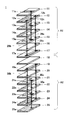
For example, an LC filter 100 disclosed in Japanese Unexamined Patent Application Publication No. 10-190391 as shown in FIG. 9 is known. Specifically, the LC filter 100 includes inductor portions 92 and 93 in which coils 86 and 87 are included, respectively. Each of the coils 86 and 87 is formed by laminating sheets in which coil conductors and via electrodes for defining a relay are provided, and their axial directions are perpendicular to input/output external electrodes 95 and 96. In addition, a ground electrode 90 and an electrode 91 are disposed in a capacitor portion 94 so as to face each other.
An end of the coil 86 is electrically connected to an end 91 a of the electrode 91 via a connection electrode 99 provided on a side surface of the filter 100 on the near side. An end of the coil 87 is electrically connected to the other end 91 b of the electrode 91 via a connection electrode 80 provided on a side surface of the filter 100 on the far side.
However, in the LC filter disclosed in Japanese Unexamined Patent Application Publication No. 10-190391, the directions of magnetic fields of the coils 86 and 87 are parallel to a board on which the LC filter is mounted. Thus, radiation of magnetic flux influences an adjacent electronic component. In addition, the coil conductors are mainly formed of pattern printing electrodes, and hence an inductance with a great Q value is not obtained. Thus, the insertion loss of the filter increases.
SUMMARY OF THE INVENTION
In view of the circumstances described above, preferred embodiments of the present invention provide an LC filter in which the direction of a magnetic field is perpendicular to a board on which the LC filter is mounted, thereby reducing the influence of radiation of magnetic flux on an adjacent electronic component, and in which an inductance with a great Q value is obtained to provide low loss.
According to a preferred embodiment of the present invention, a laminated LC filter includes a laminate including a plurality of dielectric layers, a capacitor electrode layer, an inductor electrode layer, a ground electrode layer, an input/output electrode layer, and a via electrode extending through the dielectric layers in a thickness direction thereof, and having a substantially rectangular parallelepiped shape; and an LC resonator that includes a capacitor including the capacitor electrode layer and an inductor including the inductor electrode layer. The inductor includes the inductor electrode layer and the via electrode extending through the plurality of dielectric layers in the thickness direction, and preferably has a substantially loop shape. The capacitor preferably includes the ground electrode layer and the capacitor electrode layer located so as to face the ground electrode layer. The input/output electrode layer is located on an outermost surface that faces in a lamination direction of the laminate.
According to the above configuration, the loop-shaped inductor has a structure such that the via electrode is a principal body. Thus, an inductor with a great Q value can be obtained, and as a result, it is possible to reduce the insertion loss of the filter.
In the laminated LC filter, preferably, a magnetic layer is located on a surface perpendicular to a direction of a magnetic field of the inductor among surfaces of the laminate.
According to the above configuration, the inductance of the inductor of the laminated LC filter can be increased. In addition, the magnetic layer prevents spreading of the magnetic field of the inductor, and in a device in which the laminated LC filter is mounted, influence of the magnetic field on an adjacent electronic component can be reduced. Moreover, the magnetic layer has an effect of mechanically reinforcing the laminated LC filter, due to its rigidity, and thus strength against inter-layer separation of the laminate and cracking caused by bending or the like can be increased.
In the laminated LC filter, preferably, a magnetic layer is arranged so as to extend through a loop surface of the loop-shaped inductor.
According to the above configuration, the inductance of the inductor of the laminated LC filter can be increased. In addition, the magnetic layer prevents spreading of the magnetic field of the inductor, and in a device in which the laminated LC filter is mounted, influence of the magnetic field on an adjacent electronic component can be reduced.
In the laminated LC filter, preferably, the LC resonator includes two or more LC resonators of which adjacent LC resonators are coupled to each other, and a magnetic layer is provided between the loop-shaped inductors of the adjacent LC resonators.
According to the above configuration, due to an effect of the magnetic layer preventing spreading of magnetic flux, the magnetic layer has an effect of weakening electromagnetic coupling between the inductors and can be used to adjust the electromagnetic coupling therebetween.
In the laminated LC filter, preferably, a surface parallel to the lamination direction among surfaces of the laminate is a bottom surface.
According to the above configuration, the magnetic field of the loop-shaped inductor is directed so as to be radiated from the center of the loop, and its direction is perpendicular to a board on which the laminated LC filter is mounted. Thus, influence of radiation of magnetic flux on an adjacent electronic component can be prevented and minimized.
The above and other elements, features, steps, characteristics and advantages of the present invention will become more apparent from the following detailed description of the preferred embodiments with reference to the attached drawings.
BRIEF DESCRIPTION OF THE DRAWINGS
FIG. 1 is an exploded perspective view of a laminate of a laminated LC filter according to a first preferred embodiment of the present invention.
FIGS. 2A and 2B are external perspective views of the laminated LC filter in FIG. 1.
FIG. 3 is an equivalent circuit diagram of the laminated LC filter in FIG. 1.
FIG. 4 is an exploded perspective view of a modified example of the laminated LC filter in FIG. 1.
FIG. 5 is an exploded perspective view of a laminate of a laminated LC filter according to a second preferred embodiment of the present invention.
FIGS. 6A to 6C are external perspective views of the laminated LC filter in FIG. 5.
FIGS. 7A to 7C are diagrams illustrating a laminated LC filter according to a third preferred embodiment of the present invention.
FIGS. 8A and 8B are diagrams illustrating a laminated LC filter according to a fourth preferred embodiment of the present invention.
FIG. 9 is a diagram illustrating an existing laminated LC filter.
DETAILED DESCRIPTION OF THE PREFERRED EMBODIMENTS
Hereinafter, preferred embodiments of the present invention will be described in detail with reference to the drawings.
First Preferred Embodiment
FIG. 1 is an exploded perspective view of a laminated LC filter 1 of the first preferred embodiment. FIG. 2A is an external perspective view of the laminated LC filter 1 in FIG. 1, and FIG. 2B is an external perspective view of the laminated LC filter in a state where a board (not shown) on which the laminated LC filter is mounted is located on the lower side. In FIGS. 1 to 2B, conductive films exposed to the outside are hatched.
As shown in FIG. 1, in the laminated LC filter 1 of the present preferred embodiment, a plurality of dielectric layers and electrode layers are laminated, and via electrodes extend through the dielectric layers. In all of these dielectric layers, ground electrodes are located on surfaces (hatched portions) thereof on the near side in FIG. 1 and surfaces opposed to these surfaces. The ground electrodes on the surfaces on the near side define an electrode 31 a in FIGS. 2A and 2B.
The dielectric layers 11-25 are produced, for example, preferably by applying a slurry of a ceramic dielectric material containing alumina and glass as principal components, onto a film by a doctor blade method.
The electrode layers 11 a-15 a, 17 a, 19 a, and 21 a-25 a are formed, for example, preferably by applying a photosensitive conductive paste onto the dielectric layers by a spin coat method or the like and using a photolithographic method. Alternatively, these layers may be formed by screen printing a conductive paste directly onto the dielectric layers.
Hereinafter, the laminated LC filter 1, specifically, the configurations of the laminated dielectric layers and the electrode layer and the via electrodes formed in each dielectric layer will be described in detail.
The laminated LC filter 1 preferably includes two LC resonators having the same configurations and coupled to each other. In FIG. 1, the layers from the uppermost dielectric layer 11 to the dielectric layer 17 constitute a first block A1, and the layers from the dielectric layer 18 to the lowermost dielectric layer 25 constitute a second block A2.
First, the first block A1 will be described.
In the dielectric layer 11, the input/output electrode 11 a and a portion of a via electrode 29 a are provided and connected to each other.
In the dielectric layer 12, the ground electrodes 12 a and 12 b, the inductor electrode 12 c, and portions of the via electrodes 29 a, 29 b, and 29 c are provided. The ground electrode 12 a is connected to the external ground electrodes 31 a and 31 b, the ground electrode 12 b is connected to the via electrode 29 c and the external ground electrode 31 b, and the inductor electrode 12 c is connected to the via electrodes 29 a and 29 b.
In the dielectric layer 13, the capacitor electrode 13 a and portions of the via electrodes 29 a, 29 b, and 29 c are provided. The capacitor electrode 13 a is connected to the via electrode 29 a.
In the dielectric layer 14, the ground electrode 14 a and portions of the via electrodes 29 a, 29 b, and 29 c are provided. The ground electrode 14 a is connected to the external ground electrodes 31 a and 31 b.
In the dielectric layer 15, the capacitor electrode 15 a and portions of the via electrodes 29 a, 29 b, and 29 c are provided. The capacitor electrode 15 a is connected to the via electrode 29 a.
In the dielectric layer 16, portions of the via electrodes 29 b and 29 c are provided.
In the dielectric layer 17, the inductor electrode 17 a and portions of the via electrodes 29 b and 29 c are provided. The inductor electrode 17 a is connected to the via electrodes 29 b and 29 c.
The ground electrode 12 a, the capacitor electrode 13 a, the ground electrode 14 a, and the capacitor electrode 15 a are laminated on the dielectric layers 12 to 15 in order from above. The two capacitor electrodes 13 a and 15 a are connected to each other via the via electrode 29 a to constitute a first capacitor.
Further, in the dielectric layers 12 to 17, a first inductor preferably includes a substantially loop-shaped line that extends from a connection point between the inductor electrode layer 12 c and the via electrode 29 a through the inductor electrode layer 12 c, the via electrode 29 b, the inductor electrode layer 17 a, and the via electrode 29 c in order, to a connection point between the via electrode 29 c and the ground electrode layer 12 b. As shown in FIG. 2B, when seen in an arrangement in which the laminated LC filter is mounted on a mounting board, the via electrodes extend sequentially through the dielectric layers in parallel to the mounting surface to define the inductor.
In the second block A2 in FIG. 1, dielectric layers 19-25, and electrode layers 19 and 21 a-25 a are laminated so as to be symmetrical to the first block A1 with respect to the dielectric layer 18, and via electrodes 30 a, 30 b, and 30 c are formed, to constitute a second capacitor and an inductor. As shown in FIG. 1, the lowermost layer 25 is disposed in an orientation in which the uppermost layer 11 of the first block A1 is reversed. In addition, between the first block A1 and the second block A2, a third capacitor preferably includes the inductor electrode layers 17 a and 19 a.
FIG. 3 is an equivalent circuit diagram of the laminated LC filter 1.
In FIG. 3, a capacitor C1 corresponds to the first capacitor, and an inductor L1 corresponds to the first inductor. Thus, the first capacitor C1 and the first inductor L1 constitute a first LC resonator 41. Similarly, a capacitor C2 and an inductor L2 correspond to the second capacitor and a second inductor, respectively, and constitute a second LC resonator 42. Further, a capacitor C3 corresponds to the third capacitor.
The first LC resonator 41 and the second LC resonator 42 are electromagnetically coupled to each other via the first inductor L1 and the second inductor L2.
When the laminated LC filter 1 comes into an operating state, the first and second inductors generate magnetic fields in directions perpendicular to the loop surfaces thereof. In other words, the directions of the magnetic fields are perpendicular to a lamination direction of the laminate, and are the right-left direction in FIGS. 1 and 2A and the up-down direction in FIG. 2B. Thus, the directions of the magnetic fields of the first and second inductors of the laminated LC filter 1 in the present preferred embodiment are perpendicular to the board on which the LC filter is mounted, and hence influence of radiation of magnetic flux on an adjacently mounted electronic component can be prevented.
Further, with regard to the inductors of the laminated LC filter 1 in the present preferred embodiment, the first inductor includes, as a portion of the line, the via electrodes 29 b and 29 c extending through a plurality of the dielectric layers in the thickness direction thereof, and preferably has a substantially loop shape. Normally, with regard to the diameter of each via electrode, the cross section is easily made larger than the thickness of a pattern printing electrode, and no edge corner is formed as in a pattern printing electrode. Thus, the resistance value of the via electrode can be decreased. Therefore, an inductor with a great Q value can be obtained, and it is possible to prevent the insertion loss of the laminated LC filter 1.
Further, when it is desired to increase the inductance of each inductor, the increase is possible by increasing the number of the dielectric layer 16 or 20 in FIG. 1 to lengthen the via electrodes and make the loop shape of the inductor large in size. This increase can be made without deteriorating the Q value of the inductor.
Further, in the laminated LC filter 1, the loop of each inductor preferably has a single-winding structure, but may have a double-winding structure as in a laminated LC filter 1 a shown in FIG. 4.
In the laminated LC filter 1 a, dielectric layers 111-125, and electrode layers 111 a-116 a and 121 a-125 a are laminated, and via electrodes 129 a-129 e and 130 a-130 e are provided. The basic manufacturing method and structure of the laminated LC filter 1 a and the configurations of capacitors are the same as those in the laminated LC filter 1.
A first inductor of a first block A101 preferably includes a substantially loop-shaped line that extends from a connection point between the inductor electrode layer 112 c and the via electrode 129 a through the inductor electrode layer 112 c, the via electrode 129 b, the inductor electrode layer 117 a, the via electrode 129 c, the inductor electrode 116 a, the via electrode 129 e, the inductor electrode layer 117 b, and the via electrode 129 d in order, to a connection point between the via electrode 129 d and the ground electrode layer 116 b.
A second inductor of a second block A102 is arranged so as to be symmetrical to the first inductor of the first block A101. In addition, a third capacitor preferably includes the facing inductor electrode layers 117 a and 119 a and the facing inductor electrode layers 117 b and 119 b.
According to the above configuration, the number of winding of each inductor can be changed to adjust the inductance. In addition, the number of winding of the inductor can be increased further by the arrangement of the electrode layers such as the dielectric layers 116, 116A, and 117 and the via electrodes.
Second Preferred Embodiment
A laminated LC filter 2 is obtained by adding a magnetic layer 51 to the laminated LC filter 1 of the first preferred embodiment 1. FIG. 5 is an exploded perspective view of the laminated LC filter 2, FIG. 6A is an external view of the laminated LC filter 2, and FIG. 6B is an external perspective view of the laminated LC filter 2 in a state where the laminated LC filter is mounted on a mounting board (not shown) such that the board is located on the lower side. FIG. 6C is a schematic diagram schematically illustrating a direction in which the magnetic layer 51 and dielectric layers 11 to 25 are laminated, wherein the mounting board is similarly located on the lower side.
As shown in FIGS. 5 to 6C, in the laminated LC filter 2, the magnetic layer 51 is provided on a surface parallel to the loop surfaces of the first and second inductors of the laminated LC filter 1. The magnetic fields of the inductors are perpendicular to the loop surfaces. Thus, the magnetic layer 51 is present in an area through which the magnetic fields of the first and second inductors pass, and the inductances of these inductors can be increased.
Further, spreading of the magnetic field of the inductor is inversely proportional to the magnitude of the magnetic permeability, and hence the magnetic layer 51 has an effect of preventing spreading of the magnetic field. Thus, in a device in which the laminated LC filter is mounted, the magnetic layer 51 can reduce influence of radiation of magnetic flux on an adjacent electronic component. Meanwhile, due to the effect of preventing spreading of the magnetic flux, coupling of the inductors electromagnetically coupled to each other is made loose, and the electromagnetic coupling between the first inductor L1 and the second inductor L2 is weakened.
Further, due to environmental change or the like, the laminated LC filter 2 receives a bending force in the up-down direction in FIG. 6C. This direction is parallel to the laminated surface of the laminate, and thus there is a high risk that inter-layer separation and a crack will occur due to bending. In this structure, the added magnetic layer 51 is perpendicular to the laminated surface and thus has an effect of preventing inter-layer separation and a crack from occurring.
Third Preferred Embodiment
A laminated LC filter 3 is obtained by boring the body of the laminate from the surface 32 side so as to perpendicularly extend through the loop surfaces of the first and second inductors in the laminated LC filter 1 of the first preferred embodiment, and putting a magnetic material therein to form magnetic layers 56. FIG. 7A is an external perspective view of the laminated LC filter 3, and FIG. 7B is an image diagram illustrating a state where the line of the first inductor is a loop 55 a, the line of the second inductor is a loop 55 b, and the magnetic layers 56 perpendicularly extend through the loop surfaces of these loops.
The magnetic layers 56 are located in areas through which the magnetic fields of the first and second inductors pass, and thus the inductances of these inductors can be increased. In addition, due to the effect of preventing spreading of magnetic flux, the magnetic layers 56 can reduce influence of radiation of magnetic flux on an adjacent electronic component. Meanwhile, as described above, when spreading of magnetic flux is prevented, there is also an influence that electromagnetic coupling between the first inductor L1 and the second inductor L2 is weakened.
A laminated LC filter 4 is obtained preferably by forming the magnetic layer 51 of the second preferred embodiment on the surface 32 in the laminated LC filter 3. FIG. 7C is an external perspective view of the laminated LC filter 4. As an effect resulting from the addition of the magnetic layer 51 at that time, the same effect as that described in the second preferred embodiment can be obtained.
In the present preferred embodiment of the present invention, the magnetic layers 56 are shown preferably having a substantially cylindrical shape, but their shapes may be substantially rectangular parallelepipeds or substantially polyhedrons and their sizes are not limited as long as they are located within the loops forming the inductors.
Fourth Preferred Embodiment
A laminated LC filter 5 is obtained preferably by boring the body of the laminate in the laminated LC filter 1 of the first preferred embodiment so as to extend from the surface 32 between the first and second inductors, and putting a magnetic material therein to form a magnetic layer 58. FIG. 8A is an external perspective view of the laminated LC filter 5, and FIG. 8B is an image diagram illustrating a state where the magnetic layer 58 is provided between the first inductor loop 55 a and the second inductor loop 55 b.
Due to the effect of preventing spreading of magnetic flux as described above, the magnetic layer 58 has an effect of weakening the electromagnetic coupling between the first inductor L1 and the second inductor L2 and can be used to adjust the electromagnetic coupling therebetween.
In the laminated LC filter 5, it is possible to use both or at least one of the magnetic layer 51 shown in the second preferred embodiment and the magnetic layers 56 shown in the third preferred embodiment. In this case, the effects of each layer can be obtained.
In the present preferred embodiment, the magnetic layer 58 is shown as preferably having a substantially cylindrical shape, but its shape may be a substantially rectangular parallelepiped or a substantially polyhedron and its size is not limited as long as it is located between the loops defining the inductors.
While preferred embodiments of the present invention have been described above, it is to be understood that variations and modifications will be apparent to those skilled in the art without departing from the scope and spirit of the present invention. The scope of the present invention, therefore, is to be determined solely by the following claims.

Claims (5)

What is claimed is:
1. A laminated LC filter comprising:
a laminate including a plurality of dielectric layers, a capacitor electrode layer, a first inductor electrode layer, a ground electrode layer, a pair of input/output electrode layers, and a via electrode extending through the dielectric layers in a thickness direction thereof, and having a substantially rectangular parallelepiped shape;
a first LC resonator including a first capacitor including the capacitor electrode layer and a first inductor including the first inductor electrode layer;
a second LC resonator including a second capacitor and a second inductor including a second inductor electrode layer facing the first inductor electrode layer; and
a third capacitor including the first and second inductor electrode layers;
the first inductor includes the first inductor electrode layer and the via electrode extending through the plurality of dielectric layers in the thickness direction, and has a substantially loop shape;
the first capacitor includes the ground electrode layer and the capacitor electrode layer facing the ground electrode layer; and
one of the pair of input/output electrode layers is disposed on a first outermost surface of the laminate in a direction in which the plurality of dielectric layers are laminated and another one of the pair of input/output electrode layers is disposed on a second outermost surface of the laminate opposite to the first outermost surface of the laminate in the direction in which the plurality of dielectric layers are laminated;
the first and second inductors generate magnetic fields in directions that are perpendicular or substantially perpendicular to loop surfaces thereof; and
the first and second LC resonators are adjacent to each other in the thickness direction.
2. The laminated LC filter according to claim 1, wherein a magnetic layer is located on a surface perpendicular to the direction of the magnetic field of the first inductor among surfaces of the laminate.
3. The laminated LC filter according to claim 1, wherein the first inductor is loop-shaped and a magnetic layer extends through an opening surface of the loop-shaped inductor.
4. The laminated LC filter according to claim 1, wherein the first and second LC resonators are coupled to each other, and a magnetic layer is located between loop-shaped inductors of the first and second LC resonators.
5. The laminated LC filter according to claim 1, wherein a surface parallel to a lamination direction among surfaces of the laminate is a bottom surface.
US13/290,179 2010-11-09 2011-11-07 Laminated LC filter Active 2032-11-17 US8884721B2 (en)

Applications Claiming Priority (2)

Application Number Priority Date Filing Date Title
JP2010-251291 2010-11-09
JP2010251291A JP5387542B2 (en) 2010-11-09 2010-11-09 Multilayer LC filter

Publications (2)

Publication Number Publication Date
US20120112856A1 US20120112856A1 (en) 2012-05-10
US8884721B2 true US8884721B2 (en) 2014-11-11

Family

ID=46019070

Family Applications (1)

Application Number Title Priority Date Filing Date
US13/290,179 Active 2032-11-17 US8884721B2 (en) 2010-11-09 2011-11-07 Laminated LC filter

Country Status (2)

Country Link
US (1) US8884721B2 (en)
JP (1) JP5387542B2 (en)

Cited By (1)

* Cited by examiner, † Cited by third party
Publication number Priority date Publication date Assignee Title
US20140247192A1 (en) * 2012-02-01 2014-09-04 Murata Manufacturing Co., Ltd. Wireless communication module and communication terminal apparatus incorporating the same

Families Citing this family (5)

* Cited by examiner, † Cited by third party
Publication number Priority date Publication date Assignee Title
JP6624026B2 (en) * 2016-05-20 2019-12-25 株式会社村田製作所 Laminated electronic components
TWI643454B (en) * 2016-10-05 2018-12-01 日商村田製作所股份有限公司 Multilayer LC filter
TWI656731B (en) * 2016-12-04 2019-04-11 日商村田製作所股份有限公司 Multilayer LC filter
CN109887708B (en) * 2017-11-29 2021-04-09 株式会社村田制作所 Electronic component
JP7115235B2 (en) * 2018-11-08 2022-08-09 株式会社村田製作所 Electronic component and method for manufacturing electronic component

Citations (8)

* Cited by examiner, † Cited by third party
Publication number Priority date Publication date Assignee Title
JPH03274814A (en) 1990-03-23 1991-12-05 Toko Inc Laminate type resonator and filter using the same
JPH0935936A (en) 1995-07-19 1997-02-07 Murata Mfg Co Ltd Electronic part with built-in inductor
JPH10190391A (en) 1996-12-27 1998-07-21 Murata Mfg Co Ltd Lamination type lc filter
JPH1126241A (en) 1996-11-21 1999-01-29 Tdk Corp Laminated electronic component and manufacture thereof
JP2002252117A (en) 2000-12-19 2002-09-06 Murata Mfg Co Ltd Laminated coil component and its manufacturing method
JP2005340586A (en) 2004-05-28 2005-12-08 Murata Mfg Co Ltd Laminate electronic component
JP2009246889A (en) 2008-03-31 2009-10-22 Tdk Corp Multi-layer type electronic component
US20090309683A1 (en) * 2008-06-16 2009-12-17 Cochran William T Sensor inductors, sensors for monitoring movements and positioning, apparatus, systems and methods therefore

Patent Citations (10)

* Cited by examiner, † Cited by third party
Publication number Priority date Publication date Assignee Title
JPH03274814A (en) 1990-03-23 1991-12-05 Toko Inc Laminate type resonator and filter using the same
JPH0935936A (en) 1995-07-19 1997-02-07 Murata Mfg Co Ltd Electronic part with built-in inductor
US6222427B1 (en) 1995-07-19 2001-04-24 Murata Manufacturing Co., Ltd. Inductor built-in electronic parts using via holes
JPH1126241A (en) 1996-11-21 1999-01-29 Tdk Corp Laminated electronic component and manufacture thereof
US6147573A (en) * 1996-11-21 2000-11-14 Tdk Corporation Multilayer electronic part with planar terminal electrodes
JPH10190391A (en) 1996-12-27 1998-07-21 Murata Mfg Co Ltd Lamination type lc filter
JP2002252117A (en) 2000-12-19 2002-09-06 Murata Mfg Co Ltd Laminated coil component and its manufacturing method
JP2005340586A (en) 2004-05-28 2005-12-08 Murata Mfg Co Ltd Laminate electronic component
JP2009246889A (en) 2008-03-31 2009-10-22 Tdk Corp Multi-layer type electronic component
US20090309683A1 (en) * 2008-06-16 2009-12-17 Cochran William T Sensor inductors, sensors for monitoring movements and positioning, apparatus, systems and methods therefore

Non-Patent Citations (2)

* Cited by examiner, † Cited by third party
Title
Machine translation of JP 11-026241, translated May 29, 2014. *
Official Communication issued in corresponding Japanese Patent Application No. 2010-251291, mailed on Dec. 11, 2012.

Cited By (4)

* Cited by examiner, † Cited by third party
Publication number Priority date Publication date Assignee Title
US20140247192A1 (en) * 2012-02-01 2014-09-04 Murata Manufacturing Co., Ltd. Wireless communication module and communication terminal apparatus incorporating the same
US9496597B2 (en) * 2012-02-01 2016-11-15 Murata Manufacturing Co., Ltd. Wireless communication module and communication terminal apparatus incorporating the same
US20170033444A1 (en) * 2012-02-01 2017-02-02 Murata Manufacturing Co., Ltd. Wireless communication module and communication terminal apparatus incorporating the same
US9793600B2 (en) * 2012-02-01 2017-10-17 Murata Manufacturing Co., Ltd. Wireless communication module and communication terminal apparatus incorporating the same

Also Published As

Publication number Publication date
JP5387542B2 (en) 2014-01-15
US20120112856A1 (en) 2012-05-10
JP2012105026A (en) 2012-05-31

Similar Documents

Publication Publication Date Title
US8884721B2 (en) Laminated LC filter
US9251943B2 (en) Multilayer type inductor and method of manufacturing the same
JP3127792B2 (en) LC resonator and LC filter
JP5787760B2 (en) filter
US7453344B2 (en) Multilayer coil component
JP4983881B2 (en) Multilayer bandpass filter
WO2013058144A1 (en) Composite electronic component
JP6801826B2 (en) Filter element
US8289104B2 (en) Electronic component
US9479136B2 (en) Electronic component
US8169288B2 (en) Electronic component and method for making the same
US20060022770A1 (en) Lamination type electronic component
JP7238937B2 (en) Coil parts and filter circuits including them
US8878632B2 (en) Laminated filter
KR20160032581A (en) Inductor array chip and board for mounting the same
JP2007259026A (en) Multilayer noise filter
EP1564761A1 (en) Laminated coil component and method of producing the same
JP2005150168A (en) Laminated coil component
CN215342186U (en) Coil component and filter circuit including the same
US9634633B2 (en) Electronic component
JP2008271204A (en) Laminated electronic component
US6551426B2 (en) Manufacturing method for a laminated ceramic electronic component
JPH0669038A (en) Chip-shaped coil
JP2003217935A (en) Layered inductor array
JP2000260621A (en) Stacked type common mode choke coil

Legal Events

Date Code Title Description
AS Assignment

Owner name: MURATA MANUFACTURING CO., LTD., JAPAN

Free format text: ASSIGNMENT OF ASSIGNORS INTEREST;ASSIGNOR:MIZOGUCHI, NAOKI;REEL/FRAME:027182/0572

Effective date: 20111103

STCF Information on status: patent grant

Free format text: PATENTED CASE

FEPP Fee payment procedure

Free format text: PAYOR NUMBER ASSIGNED (ORIGINAL EVENT CODE: ASPN); ENTITY STATUS OF PATENT OWNER: LARGE ENTITY

FEPP Fee payment procedure

Free format text: PAYER NUMBER DE-ASSIGNED (ORIGINAL EVENT CODE: RMPN); ENTITY STATUS OF PATENT OWNER: LARGE ENTITY

Free format text: PAYOR NUMBER ASSIGNED (ORIGINAL EVENT CODE: ASPN); ENTITY STATUS OF PATENT OWNER: LARGE ENTITY

MAFP Maintenance fee payment

Free format text: PAYMENT OF MAINTENANCE FEE, 4TH YEAR, LARGE ENTITY (ORIGINAL EVENT CODE: M1551)

Year of fee payment: 4

MAFP Maintenance fee payment

Free format text: PAYMENT OF MAINTENANCE FEE, 8TH YEAR, LARGE ENTITY (ORIGINAL EVENT CODE: M1552); ENTITY STATUS OF PATENT OWNER: LARGE ENTITY

Year of fee payment: 8