US8853559B2 - Insulation circuit board, and power semiconductor device or inverter module using the same - Google Patents
Insulation circuit board, and power semiconductor device or inverter module using the same Download PDFInfo
- Publication number
- US8853559B2 US8853559B2 US13/388,450 US201013388450A US8853559B2 US 8853559 B2 US8853559 B2 US 8853559B2 US 201013388450 A US201013388450 A US 201013388450A US 8853559 B2 US8853559 B2 US 8853559B2
- Authority
- US
- United States
- Prior art keywords
- wiring pattern
- wiring patterns
- circuit board
- insulation layer
- insulation
- Prior art date
- Legal status (The legal status is an assumption and is not a legal conclusion. Google has not performed a legal analysis and makes no representation as to the accuracy of the status listed.)
- Active, expires
Links
Images


Classifications
-
- H—ELECTRICITY
- H05—ELECTRIC TECHNIQUES NOT OTHERWISE PROVIDED FOR
- H05K—PRINTED CIRCUITS; CASINGS OR CONSTRUCTIONAL DETAILS OF ELECTRIC APPARATUS; MANUFACTURE OF ASSEMBLAGES OF ELECTRICAL COMPONENTS
- H05K1/00—Printed circuits
- H05K1/02—Details
- H05K1/03—Use of materials for the substrate
- H05K1/05—Insulated conductive substrates, e.g. insulated metal substrate
- H05K1/056—Insulated conductive substrates, e.g. insulated metal substrate the metal substrate being covered by an organic insulating layer
-
- H—ELECTRICITY
- H01—ELECTRIC ELEMENTS
- H01L—SEMICONDUCTOR DEVICES NOT COVERED BY CLASS H10
- H01L23/00—Details of semiconductor or other solid state devices
- H01L23/12—Mountings, e.g. non-detachable insulating substrates
- H01L23/14—Mountings, e.g. non-detachable insulating substrates characterised by the material or its electrical properties
- H01L23/142—Metallic substrates having insulating layers
-
- H—ELECTRICITY
- H01—ELECTRIC ELEMENTS
- H01L—SEMICONDUCTOR DEVICES NOT COVERED BY CLASS H10
- H01L23/00—Details of semiconductor or other solid state devices
- H01L23/58—Structural electrical arrangements for semiconductor devices not otherwise provided for, e.g. in combination with batteries
- H01L23/62—Protection against overvoltage, e.g. fuses, shunts
-
- H—ELECTRICITY
- H01—ELECTRIC ELEMENTS
- H01L—SEMICONDUCTOR DEVICES NOT COVERED BY CLASS H10
- H01L23/00—Details of semiconductor or other solid state devices
- H01L23/58—Structural electrical arrangements for semiconductor devices not otherwise provided for, e.g. in combination with batteries
- H01L23/64—Impedance arrangements
- H01L23/647—Resistive arrangements
-
- H—ELECTRICITY
- H01—ELECTRIC ELEMENTS
- H01L—SEMICONDUCTOR DEVICES NOT COVERED BY CLASS H10
- H01L25/00—Assemblies consisting of a plurality of individual semiconductor or other solid state devices ; Multistep manufacturing processes thereof
- H01L25/03—Assemblies consisting of a plurality of individual semiconductor or other solid state devices ; Multistep manufacturing processes thereof all the devices being of a type provided for in the same subgroup of groups H01L27/00 - H01L33/00, or in a single subclass of H10K, H10N, e.g. assemblies of rectifier diodes
- H01L25/04—Assemblies consisting of a plurality of individual semiconductor or other solid state devices ; Multistep manufacturing processes thereof all the devices being of a type provided for in the same subgroup of groups H01L27/00 - H01L33/00, or in a single subclass of H10K, H10N, e.g. assemblies of rectifier diodes the devices not having separate containers
- H01L25/07—Assemblies consisting of a plurality of individual semiconductor or other solid state devices ; Multistep manufacturing processes thereof all the devices being of a type provided for in the same subgroup of groups H01L27/00 - H01L33/00, or in a single subclass of H10K, H10N, e.g. assemblies of rectifier diodes the devices not having separate containers the devices being of a type provided for in group H01L29/00
- H01L25/072—Assemblies consisting of a plurality of individual semiconductor or other solid state devices ; Multistep manufacturing processes thereof all the devices being of a type provided for in the same subgroup of groups H01L27/00 - H01L33/00, or in a single subclass of H10K, H10N, e.g. assemblies of rectifier diodes the devices not having separate containers the devices being of a type provided for in group H01L29/00 the devices being arranged next to each other
-
- H—ELECTRICITY
- H01—ELECTRIC ELEMENTS
- H01L—SEMICONDUCTOR DEVICES NOT COVERED BY CLASS H10
- H01L25/00—Assemblies consisting of a plurality of individual semiconductor or other solid state devices ; Multistep manufacturing processes thereof
- H01L25/18—Assemblies consisting of a plurality of individual semiconductor or other solid state devices ; Multistep manufacturing processes thereof the devices being of types provided for in two or more different subgroups of the same main group of groups H01L27/00 - H01L33/00, or in a single subclass of H10K, H10N
-
- H—ELECTRICITY
- H05—ELECTRIC TECHNIQUES NOT OTHERWISE PROVIDED FOR
- H05K—PRINTED CIRCUITS; CASINGS OR CONSTRUCTIONAL DETAILS OF ELECTRIC APPARATUS; MANUFACTURE OF ASSEMBLAGES OF ELECTRICAL COMPONENTS
- H05K1/00—Printed circuits
- H05K1/02—Details
- H05K1/0213—Electrical arrangements not otherwise provided for
- H05K1/0254—High voltage adaptations; Electrical insulation details; Overvoltage or electrostatic discharge protection ; Arrangements for regulating voltages or for using plural voltages
- H05K1/0257—Overvoltage protection
-
- H—ELECTRICITY
- H05—ELECTRIC TECHNIQUES NOT OTHERWISE PROVIDED FOR
- H05K—PRINTED CIRCUITS; CASINGS OR CONSTRUCTIONAL DETAILS OF ELECTRIC APPARATUS; MANUFACTURE OF ASSEMBLAGES OF ELECTRICAL COMPONENTS
- H05K1/00—Printed circuits
- H05K1/02—Details
- H05K1/03—Use of materials for the substrate
- H05K1/05—Insulated conductive substrates, e.g. insulated metal substrate
- H05K1/053—Insulated conductive substrates, e.g. insulated metal substrate the metal substrate being covered by an inorganic insulating layer
-
- H—ELECTRICITY
- H01—ELECTRIC ELEMENTS
- H01L—SEMICONDUCTOR DEVICES NOT COVERED BY CLASS H10
- H01L23/00—Details of semiconductor or other solid state devices
- H01L23/48—Arrangements for conducting electric current to or from the solid state body in operation, e.g. leads, terminal arrangements ; Selection of materials therefor
- H01L23/488—Arrangements for conducting electric current to or from the solid state body in operation, e.g. leads, terminal arrangements ; Selection of materials therefor consisting of soldered or bonded constructions
- H01L23/498—Leads, i.e. metallisations or lead-frames on insulating substrates, e.g. chip carriers
- H01L23/49838—Geometry or layout
- H01L23/49844—Geometry or layout for devices being provided for in H01L29/00
-
- H—ELECTRICITY
- H01—ELECTRIC ELEMENTS
- H01L—SEMICONDUCTOR DEVICES NOT COVERED BY CLASS H10
- H01L2924/00—Indexing scheme for arrangements or methods for connecting or disconnecting semiconductor or solid-state bodies as covered by H01L24/00
- H01L2924/0001—Technical content checked by a classifier
- H01L2924/0002—Not covered by any one of groups H01L24/00, H01L24/00 and H01L2224/00
-
- H—ELECTRICITY
- H01—ELECTRIC ELEMENTS
- H01L—SEMICONDUCTOR DEVICES NOT COVERED BY CLASS H10
- H01L2924/00—Indexing scheme for arrangements or methods for connecting or disconnecting semiconductor or solid-state bodies as covered by H01L24/00
- H01L2924/095—Indexing scheme for arrangements or methods for connecting or disconnecting semiconductor or solid-state bodies as covered by H01L24/00 with a principal constituent of the material being a combination of two or more materials provided in the groups H01L2924/013 - H01L2924/0715
- H01L2924/097—Glass-ceramics, e.g. devitrified glass
- H01L2924/09701—Low temperature co-fired ceramic [LTCC]
-
- H—ELECTRICITY
- H01—ELECTRIC ELEMENTS
- H01L—SEMICONDUCTOR DEVICES NOT COVERED BY CLASS H10
- H01L2924/00—Indexing scheme for arrangements or methods for connecting or disconnecting semiconductor or solid-state bodies as covered by H01L24/00
- H01L2924/10—Details of semiconductor or other solid state devices to be connected
- H01L2924/11—Device type
- H01L2924/12—Passive devices, e.g. 2 terminal devices
- H01L2924/1204—Optical Diode
- H01L2924/12044—OLED
-
- H—ELECTRICITY
- H02—GENERATION; CONVERSION OR DISTRIBUTION OF ELECTRIC POWER
- H02M—APPARATUS FOR CONVERSION BETWEEN AC AND AC, BETWEEN AC AND DC, OR BETWEEN DC AND DC, AND FOR USE WITH MAINS OR SIMILAR POWER SUPPLY SYSTEMS; CONVERSION OF DC OR AC INPUT POWER INTO SURGE OUTPUT POWER; CONTROL OR REGULATION THEREOF
- H02M7/00—Conversion of ac power input into dc power output; Conversion of dc power input into ac power output
- H02M7/003—Constructional details, e.g. physical layout, assembly, wiring or busbar connections
-
- H—ELECTRICITY
- H05—ELECTRIC TECHNIQUES NOT OTHERWISE PROVIDED FOR
- H05K—PRINTED CIRCUITS; CASINGS OR CONSTRUCTIONAL DETAILS OF ELECTRIC APPARATUS; MANUFACTURE OF ASSEMBLAGES OF ELECTRICAL COMPONENTS
- H05K1/00—Printed circuits
- H05K1/02—Details
- H05K1/0201—Thermal arrangements, e.g. for cooling, heating or preventing overheating
- H05K1/0203—Cooling of mounted components
- H05K1/0204—Cooling of mounted components using means for thermal conduction connection in the thickness direction of the substrate
-
- H—ELECTRICITY
- H05—ELECTRIC TECHNIQUES NOT OTHERWISE PROVIDED FOR
- H05K—PRINTED CIRCUITS; CASINGS OR CONSTRUCTIONAL DETAILS OF ELECTRIC APPARATUS; MANUFACTURE OF ASSEMBLAGES OF ELECTRICAL COMPONENTS
- H05K1/00—Printed circuits
- H05K1/02—Details
- H05K1/0213—Electrical arrangements not otherwise provided for
- H05K1/0254—High voltage adaptations; Electrical insulation details; Overvoltage or electrostatic discharge protection ; Arrangements for regulating voltages or for using plural voltages
- H05K1/0256—Electrical insulation details, e.g. around high voltage areas
-
- H—ELECTRICITY
- H05—ELECTRIC TECHNIQUES NOT OTHERWISE PROVIDED FOR
- H05K—PRINTED CIRCUITS; CASINGS OR CONSTRUCTIONAL DETAILS OF ELECTRIC APPARATUS; MANUFACTURE OF ASSEMBLAGES OF ELECTRICAL COMPONENTS
- H05K1/00—Printed circuits
- H05K1/02—Details
- H05K1/0213—Electrical arrangements not otherwise provided for
- H05K1/0254—High voltage adaptations; Electrical insulation details; Overvoltage or electrostatic discharge protection ; Arrangements for regulating voltages or for using plural voltages
- H05K1/0262—Arrangements for regulating voltages or for using plural voltages
-
- H—ELECTRICITY
- H05—ELECTRIC TECHNIQUES NOT OTHERWISE PROVIDED FOR
- H05K—PRINTED CIRCUITS; CASINGS OR CONSTRUCTIONAL DETAILS OF ELECTRIC APPARATUS; MANUFACTURE OF ASSEMBLAGES OF ELECTRICAL COMPONENTS
- H05K2201/00—Indexing scheme relating to printed circuits covered by H05K1/00
- H05K2201/01—Dielectrics
- H05K2201/0137—Materials
- H05K2201/0154—Polyimide
-
- H—ELECTRICITY
- H05—ELECTRIC TECHNIQUES NOT OTHERWISE PROVIDED FOR
- H05K—PRINTED CIRCUITS; CASINGS OR CONSTRUCTIONAL DETAILS OF ELECTRIC APPARATUS; MANUFACTURE OF ASSEMBLAGES OF ELECTRICAL COMPONENTS
- H05K2201/00—Indexing scheme relating to printed circuits covered by H05K1/00
- H05K2201/01—Dielectrics
- H05K2201/0137—Materials
- H05K2201/0162—Silicon containing polymer, e.g. silicone
-
- H—ELECTRICITY
- H05—ELECTRIC TECHNIQUES NOT OTHERWISE PROVIDED FOR
- H05K—PRINTED CIRCUITS; CASINGS OR CONSTRUCTIONAL DETAILS OF ELECTRIC APPARATUS; MANUFACTURE OF ASSEMBLAGES OF ELECTRICAL COMPONENTS
- H05K2201/00—Indexing scheme relating to printed circuits covered by H05K1/00
- H05K2201/02—Fillers; Particles; Fibers; Reinforcement materials
- H05K2201/0203—Fillers and particles
- H05K2201/0206—Materials
- H05K2201/0209—Inorganic, non-metallic particles
-
- H—ELECTRICITY
- H05—ELECTRIC TECHNIQUES NOT OTHERWISE PROVIDED FOR
- H05K—PRINTED CIRCUITS; CASINGS OR CONSTRUCTIONAL DETAILS OF ELECTRIC APPARATUS; MANUFACTURE OF ASSEMBLAGES OF ELECTRICAL COMPONENTS
- H05K2201/00—Indexing scheme relating to printed circuits covered by H05K1/00
- H05K2201/07—Electric details
- H05K2201/0753—Insulation
- H05K2201/0761—Insulation resistance, e.g. of the surface of the PCB between the conductors
-
- H—ELECTRICITY
- H05—ELECTRIC TECHNIQUES NOT OTHERWISE PROVIDED FOR
- H05K—PRINTED CIRCUITS; CASINGS OR CONSTRUCTIONAL DETAILS OF ELECTRIC APPARATUS; MANUFACTURE OF ASSEMBLAGES OF ELECTRICAL COMPONENTS
- H05K2201/00—Indexing scheme relating to printed circuits covered by H05K1/00
- H05K2201/09—Shape and layout
- H05K2201/09209—Shape and layout details of conductors
- H05K2201/09654—Shape and layout details of conductors covering at least two types of conductors provided for in H05K2201/09218 - H05K2201/095
- H05K2201/09781—Dummy conductors, i.e. not used for normal transport of current; Dummy electrodes of components
-
- H—ELECTRICITY
- H05—ELECTRIC TECHNIQUES NOT OTHERWISE PROVIDED FOR
- H05K—PRINTED CIRCUITS; CASINGS OR CONSTRUCTIONAL DETAILS OF ELECTRIC APPARATUS; MANUFACTURE OF ASSEMBLAGES OF ELECTRICAL COMPONENTS
- H05K2201/00—Indexing scheme relating to printed circuits covered by H05K1/00
- H05K2201/10—Details of components or other objects attached to or integrated in a printed circuit board
- H05K2201/10007—Types of components
- H05K2201/10022—Non-printed resistor
Definitions
- the invention relates to a high-voltage insulation circuit board which is used in an electric power apparatus such as an electric power converter or the like such as power semiconductor device, inverter module, or the like and to a power semiconductor device or inverter module using such an insulation circuit board.
- a ceramic board having excellent heat radiation performance and heat resistance is a main stream.
- a shift to a resin board in which a high radiation insulation resin is used for an insulation layer is increasing year by year.
- a plurality of semiconductor elements and passive elements are arranged on the wiring patterns 3 on the insulation circuit board.
- a high power switching element such as an insulated-gate bipolar transistor (IGBT) or the like is used as a power semiconductor device for electric power conversion or an inverter module in recent years, there is a problem of an excessive heat generation.
- an inorganic filler is filled into the resin of the insulation layer 2 at a high density or a thickness of insulation layer 2 is made thin, thereby improving the thermal conductivity of the insulation layer 2 .
- an insulation circuit board in which an alumina filler of 70 Vol % or more was mixed into the insulation resin which is in contact with the metal base substrate 1 has also been developed, and high thermal conductivity which reaches 10 W/mk has been realized.
- an insulation circuit board using the insulation layer 2 having a layer thickness of about 200 ⁇ mt or having the smallest layer thickness of about 100 ⁇ mt has been developed.
- a high voltage associated with the realization of the recent high power is always applied to such an insulation circuit board, such a problem that a dielectric breakdown occurs for a short time can occur.
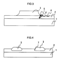
- FIG. 3 In the wiring pattern 3 to which the high voltage is applied, the generation of partial discharging 4 that is caused by electric field concentration at end sections of the wiring pattern 3 is a main cause. Particularly, in the case of an AC voltage in which a polarity of the applied voltage changes continuously, the discharge occurs continuously, so that the insulation layer 2 is deteriorated, a dendritic discharge deterioration trace called a tree 5 is formed, and a dielectric breakdown occurs soon.
- the insulation circuit board is characterized in that the insulation layer which is in contact with the metal base substrate and the wiring patterns is one of a resin mainly consisting of an epoxy resin, a resin mainly consisting of a polyimide resin, a resin mainly consisting of a silicone resin, a resin mainly consisting of an acrylic resin, and a resin mainly consisting of an urethane resin or a resin consisting of a denatured material or mixture of those resins.
- the insulation circuit board is characterized in that an inorganic filler which is dispersed into the insulation layer which is in contact with the metal base substrate and the wiring patterns is one of Al 2 O 3 (alumina), SiO 2 (silica), AlN (aluminum nitride), BN (boron nitride), ZnO (zinc oxide), SiC (silicon carbide), Si 3 N 4 (silicon nitride), and MgO (magnesium oxide), a filler adapted to improve heat radiation performance and insulation performance in a manner similar to those compounds, or a mixture of two or more kinds of those compounds.
- an inorganic filler which is dispersed into the insulation layer which is in contact with the metal base substrate and the wiring patterns is one of Al 2 O 3 (alumina), SiO 2 (silica), AlN (aluminum nitride), BN (boron nitride), ZnO (zinc oxide), SiC (silicon carbide), Si 3 N 4 (silicon nitride
- the insulation circuit board is characterized in that the insulation layer which is in contact with the metal base substrate and the wiring patterns is one of ceramic materials each mainly consisting of Al 2 O 3 (alumina), ZrO 2 (zirconia), AlN (aluminum nitride), or BN (boron nitride), a ceramic material which has characteristics similar to those of those ceramic materials, whose fundamental component consists of a metal oxide, and which is burned and solidified by a heat treatment of a high temperature, or an inorganic material consisting of a denatured material or mixture obtained by mixing a glass component into the ceramic material.
- ceramic materials each mainly consisting of Al 2 O 3 (alumina), ZrO 2 (zirconia), AlN (aluminum nitride), or BN (boron nitride)
- a ceramic material which has characteristics similar to those of those ceramic materials, whose fundamental component consists of a metal oxide, and which is burned and solidified by a heat treatment of a high temperature
- the insulation circuit board is characterized in that in order to provide the electric potential in the range of the potential difference between the adjacent wiring patterns, a resistor is arranged between the two adjacent wiring patterns where the electric potential difference exists.
- the insulation circuit board is characterized in that the electric potential in the range of the potential difference between the adjacent wiring patterns is provided from a circuit for forming the electric potential by a portion other than a portion on the insulation circuit board.
- a power semiconductor device comprising: a metal base substrate; wiring patterns which are formed onto at least one of surfaces of the metal base substrate through an insulation layer; and semiconductor elements connected to the wiring patterns, characterized in that between two adjacent wiring patterns in which an electric potential difference exists among the wiring patterns, at least one or more wiring patterns or conductors which are in contact with the insulation layer and have an electric potential in a range of the electric potential difference between the adjacent wiring patterns are arranged.
- the power semiconductor device is characterized in that the two adjacent wiring patterns are an input potential wiring pattern and a ground potential wiring pattern.
- the power semiconductor device is characterized in that the two adjacent wiring patterns are output wiring patterns of a three-phase alternating current connected to the semiconductor elements.
- the electric field concentration at the end sections of the wiring pattern to which a high voltage is applied is reduced and partial-discharge-resistant characteristics are improved. Therefore, even in high-density mounted wirings in which a distance between the wiring patterns is small, the insulation circuit board having the high insulation reliability can be realized by low costs. Providing of the power semiconductor device or inverter module using the insulation circuit board and having the high insulation reliability can be realized.
- FIG. 1 Cross sectional view of an insulation circuit board and wiring patterns for describing an embodiment of the invention.
- FIG. 2 Cross sectional view for explaining conventional insulation circuit board and wiring patterns.
- FIG. 3 Enlarged cross sectional view of the conventional insulation circuit board and wiring pattern and it is a cross sectional view for explaining sharp shapes of end sections of the wiring pattern, electric field concentration at the end sections of the wiring pattern, a tree deterioration, and a creeping discharge.
- FIG. 4 Cross sectional view of an insulation circuit board and wiring patterns for describing shapes of end sections of the wiring patterns in JP-A-2001-057409.
- FIG. 5 Plan view of the insulation circuit board for describing plan shapes of the wiring patterns of the invention.
- FIG. 6 Cross sectional view of an insulation circuit board and wiring patterns showing an embodiment of the invention and it is a diagram for explaining the wiring patterns having an intermediate electric potential.
- FIG. 7 Perspective view showing the embodiment of the invention and for explaining passive elements to form the intermediate electric potential and a connecting method.
- FIG. 8 Plan view of the insulation circuit board at the time when the invention is applied to an inverter circuit board for driving a motor.
- FIG. 9 Circuit diagram for explaining a circuit construction of the inverter for driving the motor.
- FIG. 10 Cross sectional analysis model view of the insulation circuit board and the wiring patterns using the embodiment of the invention.
- FIG. 11 Cross sectional analysis model view of an insulation circuit board and wiring patterns according to another embodiment of the invention.
- FIG. 12 Cross sectional analysis model view of an insulation circuit board and wiring patterns according to still another embodiment of the invention.
- FIG. 13 Cross sectional analysis model view of an insulation circuit board and wiring patterns according to further another embodiment of the invention.
- FIG. 14 Cross sectional analysis model view of conventional insulation circuit board and wiring patterns.
- FIGS. 1 and 6 are cross sectional view of an insulation circuit board according to an embodiment of the invention.
- the embodiment illustrated in FIG. 6 has such a construction that in FIG. 2 showing a conventional embodiment, between adjacent wiring patterns 31 and 33 which are away from each other by the distance R 1 between the wiring patterns, a new wiring pattern 32 is arranged at a position of a distance R 2 between the wiring patterns corresponding to an equal distance from each of the wiring patterns 31 and 33 .
- Other constructions are similar to those shown in FIG. 2 unless otherwise specified in particular.
- the embodiment of FIG. 6 differs largely from the conventional embodiment with respect to a point that the wiring pattern 32 arranged between the adjacent wiring patterns 31 and 33 in FIG. 2 is voltage-divided by two resistors 8 and has an intermediate electric potential of an electric potential difference between the wiring patterns 31 and 33 .
- the wiring pattern 31 on the high potential side in FIG. 2 has an electric potential of 1 kV and the wiring pattern 33 on the low potential side has an electric potential of 0V
- an electric potential of the wiring pattern 32 in FIG. 6 is equal to 500V and a potential difference between the wiring patterns 31 and 32 or between the wiring patterns 32 and 33 is equal to 500V.
- the potential difference between the adjacent wiring patterns 31 and 33 in the embodiment denotes a potential difference at a certain time point in the case where an electric potential which is applied to the wiring pattern 3 time-sequentially changes and the potential difference between the adjacent wiring patterns 31 and 33 changes. Therefore, even if the potential difference between the adjacent wiring patterns 31 and 33 is not high at a certain time point, in the case where the potential difference between the adjacent wiring patterns 31 and 33 is large at a different time point, such a case is incorporated in the adjacent wiring patterns 31 and 33 .
- a potential difference between the wiring pattern 31 on the high potential side and the wiring pattern 32 and a potential difference between the wiring pattern 32 and the wiring pattern 33 on the low potential side are equal to 350V or less. It is a value which is obtained from a Paschen's law. According to the Paschen's law, it is mentioned that a lowest value of the potential difference at the time of occurrence of a spark discharge in the air at an ordinary temperature in the case of presuming a parallel electric field is equal to about 350V.
- a potential difference between the adjacent wiring patterns 32 or conductors is equal to 350V or less.
- the filler such as a sealing resin or the like
- the electric field concentration at the end sections of the wiring pattern 31 on the high potential side is lightened, thereby raising a partial discharging voltage.
- the partial-discharge-resistant performance of the insulation circuit board in FIG. 2 can be improved.
- the wiring pattern 32 which is newly arranged has a material and a shape similar to those of the adjacent wiring patterns 31 and 33 . Therefore, the embodiment according to the invention can be easily realized by the conventional insulation circuit construction and forming method of the wiring patterns 3 . The insulation performance of the insulation circuit board can be improved by low costs.
- the wiring pattern 32 or conductor has a wiring pattern length R 4 or conductor length which is equal to or longer than an orientation length R 3 of the wiring patterns 31 and 33 showing the high potential difference.
- the wiring patterns 31 and 32 on the insulation circuit board by a chip resistor 81 it is sufficient to connect the wiring patterns 31 and 32 on the insulation circuit board by a chip resistor 81 and to connect the wiring patterns 32 and 33 on the insulation circuit board by a chip resistor 81 .
- the chip resistor 81 a small article whose vertical and lateral sizes are equal to 1 mm or less is also commercially available and it can be also easily mounted even in the wiring patterns 3 for high-density mounting to which applying of the invention thereto is assumed.
- the density of the wiring patterns 3 on the insulation circuit board is high and an element, for example, the chip resistor or the like to form the potential difference between the wiring patterns 31 and 33 showing the high potential difference cannot be mounted to the wiring patterns 3 on the insulation circuit board, it is sufficient to form an electric potential for the wiring pattern 32 by a portion other than the portion on the insulation circuit board.
- a bus bar wiring for supplying a power source to the insulation circuit board, a terminal portion of a capacitor for the power source, or the like corresponds to such a portion. It is sufficient to supply an input voltage including the intermediate electric potential formed there to the insulation circuit board.
- the intermediate electric potential can be easily obtained even in the insulation circuit board on which the wiring patterns are formed at a high density and the elements are mounted without a gap.
- FIG. 8 shows an embodiment in the case where the invention is applied to a power semiconductor device or inverter module having an inverter circuit board of a motor control system.
- an inverter of three-phase outputs using six switching elements 9 is used.
- a DC current from a converter is input through a smoothing capacitor and is converted into a 3-phase alternating current by the switching element 9 , thereby rotating the motor.
- a wiring construction shown in FIG. 8 here is obtained by presuming an inverter for a high output and six IGBT switching elements 9 A to 9 F and six free wheeling diodes 10 A to 10 F are mounted.
- the wiring patterns which provide the highest potential difference are the wiring patterns between the input and the ground and an output portion of the three-phase AC. Therefore, wiring patterns 32 A, 32 B, and 32 C showing the intermediate electric potential are respectively arranged into them, thereby reducing the electric field concentration at the end sections of wiring patterns 31 A, 31 B, 31 C, and 31 D on the high potential side.
- the six wiring patterns 3 on the left side in FIG. 8 are wiring patterns 11 A to 11 F for a gate signal for controlling the IGBT switching elements 9 A to 9 F, generally, since a gate signal voltage is small, the wiring pattern 32 to lighten the electric field concentration is not arranged.
- Wiring patterns 33 A to 33 D on the low potential side may be used in place of the wiring patterns 31 A to 33 D on the high potential side.
- the power semiconductor device or inverter module using the high-density mounting wirings in which the distance between the wiring patterns is small the power semiconductor device or inverter module having the high insulation reliability can be realized at low costs.
- FIG. 10 is a cross sectional model view for analyzing the insulation circuit board according to the embodiment of the invention.
- the epoxy resin (dielectric constant: 4 ) insulation layer 2 having a thickness of 2.0 mmt is formed on the metal base substrate 1 having a thickness of 2.0 mmt and an electrolytic copper foil having a thickness of 0.1 mmt is further adhered onto the insulation layer 2 .
- the wiring patterns 31 and 33 formed by the chemical etching and the wiring pattern 32 according to the invention are formed onto the copper foil.
- An inclination angle of the side surface of each of the wiring patterns 31 , 32 , and 33 is equal to 60°.
- the wiring patterns 31 and 33 are away from each other by the distance R 1 between the wiring patterns.
- the wiring pattern 32 is arranged at the position of the distance R 2 between the wiring patterns corresponding to the equal distance from each of the wiring patterns 31 and 33 .
- Electric potentials of the wiring patterns 31 , 32 , and 33 are equal to 900V, 450V, and 0V, respectively.
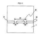
- FIG. 11 is a cross sectional model view for analyzing the insulation circuit board according another embodiment of the invention.
- the epoxy resin (dielectric constant: 4 ) insulation layer 2 having a thickness of 0.2 mmt is formed on the metal base substrate 1 having a thickness of 2.0 mmt and an electrolytic copper foil having a thickness of 0.1 mmt is further adhered onto the insulation layer 2 .
- the wiring patterns 31 and 33 formed by the chemical etching and the wiring pattern 32 according to the invention are formed onto the copper foil.
- An inclination angle of the side surface of each of the wiring patterns 31 , 32 , and 33 is equal to 60°.
- the wiring patterns 31 and 33 are away from each other by the distance R 1 between the wiring patterns.
- the wiring pattern 32 is arranged at the position of the distance R 2 between the wiring patterns corresponding to the equal distance from each of the wiring patterns 31 and 33 .
- Electric potentials of the wiring patterns 31 , 32 , and 33 are equal to 900V, 450V, and 0V, respectively.
- FIG. 12 is a cross sectional model view for analyzing the insulation circuit board according another embodiment of the invention.
- the epoxy resin (dielectric constant: 4 ) insulation layer 2 having a thickness of 0.2 mmt is formed on the metal base substrate 1 having a thickness of 2.0 mmt and an electrolytic copper foil having a thickness of 0.1 mmt is further adhered onto the insulation layer 2 .
- the wiring patterns 31 and 33 formed by the chemical etching and the wiring patterns 32 A and 32 B according to the invention are formed onto the copper foil.
- An inclination angle of the side surface of each of the wiring patterns 31 , 33 , 32 A, and 32 B is equal to 60°.
- the wiring patterns 31 and 33 are away from each other by the distance R 1 between the wiring patterns.
- the wiring patterns 32 A and 32 B are arranged at the positions of the distance R 2 between the wiring patterns corresponding to the equal distance from each of the wiring patterns 31 and 33 .
- Electric potentials of the wiring patterns 31 , 32 A, 32 B, and 33 are equal to 900V, 600V, 300V, and 0V, respectively.
- FIG. 13 is a cross sectional model view for analyzing the insulation circuit board according another embodiment of the invention.
- the epoxy resin (dielectric constant: 4 ) insulation layer 2 having a thickness of 0.2 mmt is formed on the metal base substrate 1 having a thickness of 2.0 mmt and an electrolytic copper foil having a thickness of 0.1 mmt is further adhered onto the insulation layer 2 .
- the wiring patterns 31 and 33 formed by the chemical etching and the wiring patterns 32 B and 32 A according to the invention are formed onto the copper foil.
- An inclination angle of the side surface of each of the wiring patterns 31 , 33 , 32 B, and 32 A is equal to 60°.
- the wiring patterns 31 and 33 are away from each other by the distance R 1 between the wiring patterns.
- FIG. 14 is a cross sectional model view for analysis which simulates the insulation circuit board by the conventional wiring patterns 3 .
- the epoxy resin (dielectric constant: 4 ) insulation layer 2 having a thickness of 0.2 mmt is formed on the metal base substrate 1 having a thickness of 2.0 mmt and an electrolytic copper foil having a thickness of 0.1 mmt is further adhered onto the insulation layer 2 .
- the wiring patterns 31 and 33 formed by the chemical etching are formed onto the copper foil.
- An inclination angle of the side surface of each of the wiring patterns 31 and 33 is equal to 60°.
- the wiring patterns 31 and 33 are away from each other by the distance R 1 between the wiring patterns. Further, electric potentials of the wiring patterns 31 and 33 are equal to 900V and 0V, respectively.
- the effect of the invention can be sufficiently obtained.
- the effect of the invention increases larger.
- the effect of the invention is smaller than that in the embodiment of FIG. 12 . Therefore, by arranging a larger number of wiring patterns 32 between the wiring patterns 31 and 33 showing the high potential difference and by sequentially decreasing the electric potentials of the wiring patterns 32 in the direction from the wiring pattern 31 on the high potential side toward the wiring pattern 33 on the low potential side, the effect of the invention can be obtained larger.
- FIG. 12 (distance R1 between R2 between the wiring patterns/pattern widths the wiring patterns FIG. 11 of the wiring patterns 32A and 32B) 0.25 mm 92.78% 89.34% (1.5 mm/0.375 mm) 89.25% (2.0 mm/0.625 mm) 0.5 mm 97.02% 95.83% (2.0 mm/0.25 mm)
- the distance R 2 between the wiring patterns is equal to 0.25 mm, even if the distance R 1 between the wiring patterns differs, an almost equal reducing effect is obtained. Therefore, when the distance R 2 between the wiring patterns is constant, the effect of the invention does not depend on the pattern widths of the wiring patterns 32 A and 32 B.
- the width of the wiring pattern 32 is further decreased and a larger number of wiring patterns 32 in which the electric potentials decrease sequentially in the direction from the high-potential wiring pattern 31 toward the low-potential wiring pattern 33 are arranged between the wiring patterns 31 and 33 showing the high potential difference, so that the effect of the invention can be obtained larger.
Landscapes
- Engineering & Computer Science (AREA)
- Microelectronics & Electronic Packaging (AREA)
- Power Engineering (AREA)
- Physics & Mathematics (AREA)
- Condensed Matter Physics & Semiconductors (AREA)
- General Physics & Mathematics (AREA)
- Computer Hardware Design (AREA)
- Chemical & Material Sciences (AREA)
- Inorganic Chemistry (AREA)
- Structure Of Printed Boards (AREA)
Applications Claiming Priority (3)
| Application Number | Priority Date | Filing Date | Title |
|---|---|---|---|
| JP2009-225903 | 2009-09-30 | ||
| JP2009225903A JP5542399B2 (ja) | 2009-09-30 | 2009-09-30 | 絶縁回路基板およびそれを用いたパワー半導体装置、又はインバータモジュール |
| PCT/JP2010/052847 WO2011040054A1 (fr) | 2009-09-30 | 2010-02-24 | Carte de circuit isolant, et dispositif à semi-conducteurs de puissance ou module d'onduleur utilisant cette carte |
Publications (2)
| Publication Number | Publication Date |
|---|---|
| US20120127684A1 US20120127684A1 (en) | 2012-05-24 |
| US8853559B2 true US8853559B2 (en) | 2014-10-07 |
Family
ID=43825893
Family Applications (1)
| Application Number | Title | Priority Date | Filing Date |
|---|---|---|---|
| US13/388,450 Active 2030-10-30 US8853559B2 (en) | 2009-09-30 | 2010-02-24 | Insulation circuit board, and power semiconductor device or inverter module using the same |
Country Status (5)
| Country | Link |
|---|---|
| US (1) | US8853559B2 (fr) |
| EP (1) | EP2485254A4 (fr) |
| JP (1) | JP5542399B2 (fr) |
| CN (1) | CN102473688B (fr) |
| WO (1) | WO2011040054A1 (fr) |
Families Citing this family (23)
| Publication number | Priority date | Publication date | Assignee | Title |
|---|---|---|---|---|
| US9061131B2 (en) | 2009-08-17 | 2015-06-23 | Histosonics, Inc. | Disposable acoustic coupling medium container |
| WO2011028603A2 (fr) | 2009-08-26 | 2011-03-10 | The Regents Of The University Of Michigan | Bras de commande de micromanipulateur pour transducteurs thérapeutiques et d'imagerie du type à ultrasons |
| JP5726191B2 (ja) | 2009-08-26 | 2015-05-27 | リージェンツ オブ ザ ユニバーシティー オブ ミシガン | 尿管結石の破砕の際に気泡混濁空洞現象の制御を使用する装置および方法 |
| FR2975528B1 (fr) * | 2011-05-17 | 2014-02-28 | Alstom Transport Sa | Dispositif d'isolation electrique d'un plan conducteur presentant un premier potentiel electrique par rapport a un deuxieme potentiel, comprenant des moyens de diminution de la valeur du champ electrostatique en un point du bord peripherique du plan conducteur |
| JP5895387B2 (ja) * | 2011-07-21 | 2016-03-30 | 住友電気工業株式会社 | 半導体基板加熱用基板保持体 |
| KR101262588B1 (ko) | 2011-07-28 | 2013-05-08 | 엘지이노텍 주식회사 | 에폭시 수지 조성물 및 이를 이용한 방열회로기판 |
| US9144694B2 (en) | 2011-08-10 | 2015-09-29 | The Regents Of The University Of Michigan | Lesion generation through bone using histotripsy therapy without aberration correction |
| US9049783B2 (en) * | 2012-04-13 | 2015-06-02 | Histosonics, Inc. | Systems and methods for obtaining large creepage isolation on printed circuit boards |
| EP2844343B1 (fr) | 2012-04-30 | 2018-11-21 | The Regents Of The University Of Michigan | Fabrication de transducteurs à ultrasons à l'aide d'un procédé de prototypage rapide |
| US20140100459A1 (en) | 2012-10-05 | 2014-04-10 | The Regents Of The University Of Michigan | Bubble-induced color doppler feedback during histotripsy |
| CN103050470B (zh) * | 2012-12-26 | 2016-08-10 | 美的集团股份有限公司 | 智能功率模块及其制作方法 |
| US11432900B2 (en) | 2013-07-03 | 2022-09-06 | Histosonics, Inc. | Articulating arm limiter for cavitational ultrasound therapy system |
| BR112015032926B1 (pt) | 2013-07-03 | 2022-04-05 | Histosonics, Inc. | Sistema de terapia de ultrassom |
| US10780298B2 (en) | 2013-08-22 | 2020-09-22 | The Regents Of The University Of Michigan | Histotripsy using very short monopolar ultrasound pulses |
| JP6421463B2 (ja) * | 2014-06-02 | 2018-11-14 | 日本電産リード株式会社 | 基板検査装置、及び基板検査方法 |
| US11135454B2 (en) | 2015-06-24 | 2021-10-05 | The Regents Of The University Of Michigan | Histotripsy therapy systems and methods for the treatment of brain tissue |
| DE102015221688A1 (de) | 2015-11-05 | 2017-05-11 | Osram Gmbh | Verfahren zur Reduzierung von Leiterbahnabständen bei elektronischen Leiterplatten und elektronische Leiterplatte mit reduzierten Abständen zwischen Leiterbahnen |
| EP3401957B1 (fr) | 2017-05-12 | 2021-06-30 | Infineon Technologies AG | Agencement de module semi-conducteur de puissance et son procédé de fabrication |
| WO2019107476A1 (fr) * | 2017-11-29 | 2019-06-06 | 大日本印刷株式会社 | Carte de câblage et procédé de production de carte de câblage |
| JP2022510654A (ja) | 2018-11-28 | 2022-01-27 | ヒストソニックス,インコーポレーテッド | 組織破砕システムおよび方法 |
| JP7325747B2 (ja) * | 2019-02-07 | 2023-08-15 | 積水化学工業株式会社 | 半導体装置 |
| WO2021155026A1 (fr) | 2020-01-28 | 2021-08-05 | The Regents Of The University Of Michigan | Systèmes et procédés d'immunosensibilisation par histotripsie |
| US20230275010A1 (en) * | 2020-07-06 | 2023-08-31 | Amosense Co., Ltd | Power module |
Citations (6)
| Publication number | Priority date | Publication date | Assignee | Title |
|---|---|---|---|---|
| US5384683A (en) * | 1991-11-07 | 1995-01-24 | Kabushiki Kaisha Toshiba | Intelligent power device module |
| JP2000252597A (ja) | 1999-02-25 | 2000-09-14 | Sanyo Electric Co Ltd | プリント基板 |
| JP2001057409A (ja) | 1999-08-17 | 2001-02-27 | Hitachi Ltd | 半導体装置 |
| JP2001177054A (ja) | 1999-12-20 | 2001-06-29 | Hitachi Ltd | 絶縁回路基板およびそれを用いたパワー半導体装置 |
| JP2003303940A (ja) | 2002-04-12 | 2003-10-24 | Hitachi Ltd | 絶縁回路基板および半導体装置 |
| JP2009065017A (ja) | 2007-09-07 | 2009-03-26 | Fuji Electric Device Technology Co Ltd | 信号伝送デバイス |
Family Cites Families (7)
| Publication number | Priority date | Publication date | Assignee | Title |
|---|---|---|---|---|
| US5420455A (en) * | 1994-03-31 | 1995-05-30 | International Business Machines Corp. | Array fuse damage protection devices and fabrication method |
| JPH1154658A (ja) * | 1997-07-30 | 1999-02-26 | Hitachi Ltd | 半導体装置及びその製造方法並びにフレーム構造体 |
| JP2001156408A (ja) * | 1999-11-30 | 2001-06-08 | Fujitsu Ltd | プリント回路基板および配線形成方法 |
| JP4955263B2 (ja) * | 2004-12-15 | 2012-06-20 | イビデン株式会社 | プリント配線板 |
| JP2007329387A (ja) * | 2006-06-09 | 2007-12-20 | Mitsubishi Electric Corp | 半導体装置 |
| US7598823B2 (en) * | 2007-03-08 | 2009-10-06 | Tennrich International Corp. | High-speed digital transmission signal line for providing a desired dynamic resistance |
| JP5326313B2 (ja) | 2008-03-21 | 2013-10-30 | ニプロ株式会社 | 血栓捕捉カテーテル |
-
2009
- 2009-09-30 JP JP2009225903A patent/JP5542399B2/ja not_active Expired - Fee Related
-
2010
- 2010-02-24 WO PCT/JP2010/052847 patent/WO2011040054A1/fr active Application Filing
- 2010-02-24 EP EP10820175.7A patent/EP2485254A4/fr not_active Withdrawn
- 2010-02-24 CN CN201080033856.9A patent/CN102473688B/zh not_active Expired - Fee Related
- 2010-02-24 US US13/388,450 patent/US8853559B2/en active Active
Patent Citations (7)
| Publication number | Priority date | Publication date | Assignee | Title |
|---|---|---|---|---|
| US5384683A (en) * | 1991-11-07 | 1995-01-24 | Kabushiki Kaisha Toshiba | Intelligent power device module |
| JP2000252597A (ja) | 1999-02-25 | 2000-09-14 | Sanyo Electric Co Ltd | プリント基板 |
| JP2001057409A (ja) | 1999-08-17 | 2001-02-27 | Hitachi Ltd | 半導体装置 |
| JP2001177054A (ja) | 1999-12-20 | 2001-06-29 | Hitachi Ltd | 絶縁回路基板およびそれを用いたパワー半導体装置 |
| US6504110B1 (en) | 1999-12-20 | 2003-01-07 | Hitachi, Ltd. | Insulating circuit board and power semiconductor apparatus employing the same |
| JP2003303940A (ja) | 2002-04-12 | 2003-10-24 | Hitachi Ltd | 絶縁回路基板および半導体装置 |
| JP2009065017A (ja) | 2007-09-07 | 2009-03-26 | Fuji Electric Device Technology Co Ltd | 信号伝送デバイス |
Also Published As
| Publication number | Publication date |
|---|---|
| EP2485254A4 (fr) | 2017-11-29 |
| US20120127684A1 (en) | 2012-05-24 |
| WO2011040054A1 (fr) | 2011-04-07 |
| CN102473688A (zh) | 2012-05-23 |
| CN102473688B (zh) | 2015-07-01 |
| JP5542399B2 (ja) | 2014-07-09 |
| JP2011077224A (ja) | 2011-04-14 |
| EP2485254A1 (fr) | 2012-08-08 |
Similar Documents
| Publication | Publication Date | Title |
|---|---|---|
| US8853559B2 (en) | Insulation circuit board, and power semiconductor device or inverter module using the same | |
| US11069621B2 (en) | Semiconductor device | |
| US8659920B2 (en) | Switching device provided with a flowing restriction element | |
| US10727145B2 (en) | Semiconducter device with filler to suppress generation of air bubbles and electric power converter | |
| US9893646B2 (en) | System for a low profile, low inductance power switching module | |
| JP5258721B2 (ja) | インバータ装置 | |
| US11398448B2 (en) | Semiconductor module | |
| US20180175853A1 (en) | Power Modules Having an Integrated Clamp Circuit and Process Thereof | |
| JP2001135788A (ja) | 半導体モジュール及びこれを用いたインバータ装置 | |
| KR20140126668A (ko) | 3 레벨 전력 변환기 하프 브리지 | |
| Kou et al. | Applying GaN HEMTs in conventional housing-type power modules | |
| US9445497B2 (en) | Semiconductor device | |
| Meisser et al. | Connector-less SiC power modules with integrated shunt—Low-profile design for low inductance and low cost | |
| US10079212B2 (en) | Semiconductor device having solder groove | |
| US11373988B2 (en) | Semiconductor device | |
| WO2013105456A1 (fr) | Carte de circuit imprimé et dispositif électronique | |
| US10607916B2 (en) | Substrate for semiconductor devices | |
| US10186607B2 (en) | Power semiconductor device including a semiconductor switching element | |
| US20240023299A1 (en) | Semiconductor apparatus | |
| US11239211B2 (en) | Electronic device having a curved portion between a plurality of conductive portions on a substrate | |
| CN109671633A (zh) | 一种高压igbt衬板绝缘方法 | |
| US11997834B2 (en) | Control apparatus for operating an electric drive for a vehicle having first and second power modules with a cooler therebetween and related method | |
| JP2023150211A (ja) | 高電圧印加回路 | |
| US20210068310A1 (en) | Control apparatus for operating an electric drive for a vehicle and method of manufacturing such a control apparatus |
Legal Events
| Date | Code | Title | Description |
|---|---|---|---|
| AS | Assignment |
Owner name: HITACHI, LTD., JAPAN Free format text: ASSIGNMENT OF ASSIGNORS INTEREST;ASSIGNORS:MATSUMOTO, HIRONORI;KUSUKAWA, JUMPEI;REEL/FRAME:027638/0482 Effective date: 20111215 |
|
| STCF | Information on status: patent grant |
Free format text: PATENTED CASE |
|
| MAFP | Maintenance fee payment |
Free format text: PAYMENT OF MAINTENANCE FEE, 4TH YEAR, LARGE ENTITY (ORIGINAL EVENT CODE: M1551) Year of fee payment: 4 |
|
| MAFP | Maintenance fee payment |
Free format text: PAYMENT OF MAINTENANCE FEE, 8TH YEAR, LARGE ENTITY (ORIGINAL EVENT CODE: M1552); ENTITY STATUS OF PATENT OWNER: LARGE ENTITY Year of fee payment: 8 |