US8735883B2 - Oxide thin film transistor and method of fabricating the same - Google Patents
Oxide thin film transistor and method of fabricating the same Download PDFInfo
- Publication number
- US8735883B2 US8735883B2 US13/324,751 US201113324751A US8735883B2 US 8735883 B2 US8735883 B2 US 8735883B2 US 201113324751 A US201113324751 A US 201113324751A US 8735883 B2 US8735883 B2 US 8735883B2
- Authority
- US
- United States
- Prior art keywords
- active layer
- layer
- insulating layer
- oxide semiconductor
- substrate
- Prior art date
- Legal status (The legal status is an assumption and is not a legal conclusion. Google has not performed a legal analysis and makes no representation as to the accuracy of the status listed.)
- Active
Links
- 239000010409 thin film Substances 0.000 title claims abstract description 32
- 238000004519 manufacturing process Methods 0.000 title description 4
- 239000000758 substrate Substances 0.000 claims abstract description 71
- 239000004065 semiconductor Substances 0.000 claims abstract description 60
- 238000000034 method Methods 0.000 claims abstract description 43
- 239000010408 film Substances 0.000 claims abstract description 37
- 229910052735 hafnium Inorganic materials 0.000 claims abstract description 11
- 229910052793 cadmium Inorganic materials 0.000 claims abstract description 10
- 229910052733 gallium Inorganic materials 0.000 claims abstract description 10
- 229910052738 indium Inorganic materials 0.000 claims abstract description 10
- 229910002059 quaternary alloy Inorganic materials 0.000 claims abstract description 10
- 229910052718 tin Inorganic materials 0.000 claims abstract description 10
- 229910052725 zinc Inorganic materials 0.000 claims abstract description 10
- 229910052726 zirconium Inorganic materials 0.000 claims abstract description 10
- 238000000059 patterning Methods 0.000 claims abstract description 9
- 239000010410 layer Substances 0.000 claims description 178
- QVGXLLKOCUKJST-UHFFFAOYSA-N atomic oxygen Chemical compound [O] QVGXLLKOCUKJST-UHFFFAOYSA-N 0.000 claims description 10
- 229910052760 oxygen Inorganic materials 0.000 claims description 10
- 239000001301 oxygen Substances 0.000 claims description 10
- 239000011701 zinc Substances 0.000 claims description 9
- 238000009832 plasma treatment Methods 0.000 claims description 7
- 239000011241 protective layer Substances 0.000 claims description 6
- 238000001312 dry etching Methods 0.000 claims description 5
- XLOMVQKBTHCTTD-UHFFFAOYSA-N Zinc monoxide Chemical compound [Zn]=O XLOMVQKBTHCTTD-UHFFFAOYSA-N 0.000 claims description 4
- 238000004381 surface treatment Methods 0.000 claims description 3
- 238000007669 thermal treatment Methods 0.000 claims description 3
- 239000011521 glass Substances 0.000 claims description 2
- 239000011787 zinc oxide Substances 0.000 claims description 2
- 230000008569 process Effects 0.000 description 21
- 238000000206 photolithography Methods 0.000 description 17
- 239000004973 liquid crystal related substance Substances 0.000 description 12
- 239000011810 insulating material Substances 0.000 description 10
- 238000012546 transfer Methods 0.000 description 8
- 239000004020 conductor Substances 0.000 description 7
- PXHVJJICTQNCMI-UHFFFAOYSA-N Nickel Chemical compound [Ni] PXHVJJICTQNCMI-UHFFFAOYSA-N 0.000 description 6
- BASFCYQUMIYNBI-UHFFFAOYSA-N platinum Chemical compound [Pt] BASFCYQUMIYNBI-UHFFFAOYSA-N 0.000 description 6
- VYPSYNLAJGMNEJ-UHFFFAOYSA-N Silicium dioxide Chemical compound O=[Si]=O VYPSYNLAJGMNEJ-UHFFFAOYSA-N 0.000 description 4
- 230000008901 benefit Effects 0.000 description 4
- 239000011651 chromium Substances 0.000 description 4
- 239000010949 copper Substances 0.000 description 4
- 239000000463 material Substances 0.000 description 4
- 230000001681 protective effect Effects 0.000 description 4
- 238000012360 testing method Methods 0.000 description 4
- 239000010936 titanium Substances 0.000 description 4
- 229910021417 amorphous silicon Inorganic materials 0.000 description 3
- 238000011160 research Methods 0.000 description 3
- 229910052814 silicon oxide Inorganic materials 0.000 description 3
- 239000000126 substance Substances 0.000 description 3
- 229910000838 Al alloy Inorganic materials 0.000 description 2
- VYZAMTAEIAYCRO-UHFFFAOYSA-N Chromium Chemical compound [Cr] VYZAMTAEIAYCRO-UHFFFAOYSA-N 0.000 description 2
- RYGMFSIKBFXOCR-UHFFFAOYSA-N Copper Chemical compound [Cu] RYGMFSIKBFXOCR-UHFFFAOYSA-N 0.000 description 2
- 229910001182 Mo alloy Inorganic materials 0.000 description 2
- ZOKXTWBITQBERF-UHFFFAOYSA-N Molybdenum Chemical compound [Mo] ZOKXTWBITQBERF-UHFFFAOYSA-N 0.000 description 2
- 229910052581 Si3N4 Inorganic materials 0.000 description 2
- RTAQQCXQSZGOHL-UHFFFAOYSA-N Titanium Chemical compound [Ti] RTAQQCXQSZGOHL-UHFFFAOYSA-N 0.000 description 2
- 229910052782 aluminium Inorganic materials 0.000 description 2
- XAGFODPZIPBFFR-UHFFFAOYSA-N aluminium Chemical compound [Al] XAGFODPZIPBFFR-UHFFFAOYSA-N 0.000 description 2
- 238000005229 chemical vapour deposition Methods 0.000 description 2
- 229910052804 chromium Inorganic materials 0.000 description 2
- 229910052802 copper Inorganic materials 0.000 description 2
- 238000000151 deposition Methods 0.000 description 2
- 238000011161 development Methods 0.000 description 2
- 238000005530 etching Methods 0.000 description 2
- 238000002438 flame photometric detection Methods 0.000 description 2
- 239000011159 matrix material Substances 0.000 description 2
- 229910052750 molybdenum Inorganic materials 0.000 description 2
- 239000011733 molybdenum Substances 0.000 description 2
- 229910052759 nickel Inorganic materials 0.000 description 2
- TWNQGVIAIRXVLR-UHFFFAOYSA-N oxo(oxoalumanyloxy)alumane Chemical compound O=[Al]O[Al]=O TWNQGVIAIRXVLR-UHFFFAOYSA-N 0.000 description 2
- 229920002120 photoresistant polymer Polymers 0.000 description 2
- 238000005240 physical vapour deposition Methods 0.000 description 2
- 238000000623 plasma-assisted chemical vapour deposition Methods 0.000 description 2
- 229910052697 platinum Inorganic materials 0.000 description 2
- HQVNEWCFYHHQES-UHFFFAOYSA-N silicon nitride Chemical compound N12[Si]34N5[Si]62N3[Si]51N64 HQVNEWCFYHHQES-UHFFFAOYSA-N 0.000 description 2
- 229910052715 tantalum Inorganic materials 0.000 description 2
- GUVRBAGPIYLISA-UHFFFAOYSA-N tantalum atom Chemical compound [Ta] GUVRBAGPIYLISA-UHFFFAOYSA-N 0.000 description 2
- 229910052719 titanium Inorganic materials 0.000 description 2
- WFKWXMTUELFFGS-UHFFFAOYSA-N tungsten Chemical compound [W] WFKWXMTUELFFGS-UHFFFAOYSA-N 0.000 description 2
- 229910052721 tungsten Inorganic materials 0.000 description 2
- 239000010937 tungsten Substances 0.000 description 2
- 229910004205 SiNX Inorganic materials 0.000 description 1
- 239000002253 acid Substances 0.000 description 1
- 230000004888 barrier function Effects 0.000 description 1
- 230000005540 biological transmission Effects 0.000 description 1
- 230000000903 blocking effect Effects 0.000 description 1
- 230000015556 catabolic process Effects 0.000 description 1
- 230000008859 change Effects 0.000 description 1
- 239000003086 colorant Substances 0.000 description 1
- 238000006731 degradation reaction Methods 0.000 description 1
- 230000000694 effects Effects 0.000 description 1
- VBJZVLUMGGDVMO-UHFFFAOYSA-N hafnium atom Chemical compound [Hf] VBJZVLUMGGDVMO-UHFFFAOYSA-N 0.000 description 1
- 229910000449 hafnium oxide Inorganic materials 0.000 description 1
- WIHZLLGSGQNAGK-UHFFFAOYSA-N hafnium(4+);oxygen(2-) Chemical compound [O-2].[O-2].[Hf+4] WIHZLLGSGQNAGK-UHFFFAOYSA-N 0.000 description 1
- AMGQUBHHOARCQH-UHFFFAOYSA-N indium;oxotin Chemical compound [In].[Sn]=O AMGQUBHHOARCQH-UHFFFAOYSA-N 0.000 description 1
- 238000012986 modification Methods 0.000 description 1
- 230000004048 modification Effects 0.000 description 1
- 230000003287 optical effect Effects 0.000 description 1
- 238000001020 plasma etching Methods 0.000 description 1
- 229910021420 polycrystalline silicon Inorganic materials 0.000 description 1
- 238000012545 processing Methods 0.000 description 1
- 230000004044 response Effects 0.000 description 1
- 239000000565 sealant Substances 0.000 description 1
- 239000005361 soda-lime glass Substances 0.000 description 1
- 239000002904 solvent Substances 0.000 description 1
- 238000004544 sputter deposition Methods 0.000 description 1
- 230000007704 transition Effects 0.000 description 1
- 238000002834 transmittance Methods 0.000 description 1
- 239000012780 transparent material Substances 0.000 description 1
- YVTHLONGBIQYBO-UHFFFAOYSA-N zinc indium(3+) oxygen(2-) Chemical compound [O--].[Zn++].[In+3] YVTHLONGBIQYBO-UHFFFAOYSA-N 0.000 description 1
Images


Classifications
-
- H—ELECTRICITY
- H01—ELECTRIC ELEMENTS
- H01L—SEMICONDUCTOR DEVICES NOT COVERED BY CLASS H10
- H01L29/00—Semiconductor devices adapted for rectifying, amplifying, oscillating or switching, or capacitors or resistors with at least one potential-jump barrier or surface barrier, e.g. PN junction depletion layer or carrier concentration layer; Details of semiconductor bodies or of electrodes thereof ; Multistep manufacturing processes therefor
- H01L29/66—Types of semiconductor device ; Multistep manufacturing processes therefor
- H01L29/68—Types of semiconductor device ; Multistep manufacturing processes therefor controllable by only the electric current supplied, or only the electric potential applied, to an electrode which does not carry the current to be rectified, amplified or switched
- H01L29/76—Unipolar devices, e.g. field effect transistors
- H01L29/772—Field effect transistors
- H01L29/78—Field effect transistors with field effect produced by an insulated gate
- H01L29/786—Thin film transistors, i.e. transistors with a channel being at least partly a thin film
- H01L29/7869—Thin film transistors, i.e. transistors with a channel being at least partly a thin film having a semiconductor body comprising an oxide semiconductor material, e.g. zinc oxide, copper aluminium oxide, cadmium stannate
-
- H—ELECTRICITY
- H01—ELECTRIC ELEMENTS
- H01L—SEMICONDUCTOR DEVICES NOT COVERED BY CLASS H10
- H01L27/00—Devices consisting of a plurality of semiconductor or other solid-state components formed in or on a common substrate
- H01L27/02—Devices consisting of a plurality of semiconductor or other solid-state components formed in or on a common substrate including semiconductor components specially adapted for rectifying, oscillating, amplifying or switching and having at least one potential-jump barrier or surface barrier; including integrated passive circuit elements with at least one potential-jump barrier or surface barrier
- H01L27/12—Devices consisting of a plurality of semiconductor or other solid-state components formed in or on a common substrate including semiconductor components specially adapted for rectifying, oscillating, amplifying or switching and having at least one potential-jump barrier or surface barrier; including integrated passive circuit elements with at least one potential-jump barrier or surface barrier the substrate being other than a semiconductor body, e.g. an insulating body
- H01L27/1214—Devices consisting of a plurality of semiconductor or other solid-state components formed in or on a common substrate including semiconductor components specially adapted for rectifying, oscillating, amplifying or switching and having at least one potential-jump barrier or surface barrier; including integrated passive circuit elements with at least one potential-jump barrier or surface barrier the substrate being other than a semiconductor body, e.g. an insulating body comprising a plurality of TFTs formed on a non-semiconducting substrate, e.g. driving circuits for AMLCDs
- H01L27/1222—Devices consisting of a plurality of semiconductor or other solid-state components formed in or on a common substrate including semiconductor components specially adapted for rectifying, oscillating, amplifying or switching and having at least one potential-jump barrier or surface barrier; including integrated passive circuit elements with at least one potential-jump barrier or surface barrier the substrate being other than a semiconductor body, e.g. an insulating body comprising a plurality of TFTs formed on a non-semiconducting substrate, e.g. driving circuits for AMLCDs with a particular composition, shape or crystalline structure of the active layer
- H01L27/1225—Devices consisting of a plurality of semiconductor or other solid-state components formed in or on a common substrate including semiconductor components specially adapted for rectifying, oscillating, amplifying or switching and having at least one potential-jump barrier or surface barrier; including integrated passive circuit elements with at least one potential-jump barrier or surface barrier the substrate being other than a semiconductor body, e.g. an insulating body comprising a plurality of TFTs formed on a non-semiconducting substrate, e.g. driving circuits for AMLCDs with a particular composition, shape or crystalline structure of the active layer with semiconductor materials not belonging to the group IV of the periodic table, e.g. InGaZnO
Definitions
- LCD liquid crystal display
- the LCD includes a color filter substrate, an array substrate and a liquid crystal layer formed between the color filter substrate and the array substrate.
- An active matrix (AM) driving method commonly used for the LCD is a method in which liquid crystal of a pixel part is driven by using an amorphous silicon thin film transistors (a-Si TFTs) as a switching element.
- a-Si TFTs amorphous silicon thin film transistors
- FIG. 1 is an exploded perspective view showing a related art LCD device.
- the LCD includes a color filter substrate 5 , an array substrate 10 and a liquid crystal layer 30 formed between the color filter substrate 5 and the array substrate 10 .
- the color filter substrate 5 includes a color filter (C) including a plurality of sub-color filters 7 that implement red, green and blue colors, a black matrix 6 for demarcating the sub-color filters 7 and blocking light transmission through the liquid crystal layer 30 , and a transparent common electrode 8 for applying a voltage to the liquid crystal layer 30 .
- C color filter
- the array substrate 10 includes a plurality of gate lines 16 and a plurality of data lines 17 which are arranged vertically and horizontally to define a plurality of pixel regions (P), TFTs (T), switching elements, formed at respective crossings of the gate lines 16 and the data lines 17 , and pixel electrodes 18 formed on the pixel regions (P).
- the color filter substrate 5 and the array substrate 10 are attached in a facing manner by a sealant formed at the edges of an image display area to form a liquid crystal panel, and the attachment of the color filter substrate 5 and the array substrate 10 is made by attachment keys formed on the color filter substrate 5 or the array substrate 10 .
- the above-described LCD is a display device which has come into prominence so far with its advantages of being light and consuming a small amount of power, but it is a light receiving device, not a light emitting device, and has a technical limitation with respect to brightness, a contrast ratio, a viewing angle, and the like.
- development of a new display device that may overcome such shortcomings is actively ongoing.
- OLED organic light emitting diode
- LCD liquid crystal display
- the amorphous silicon thin film transistor used for the above-described LCD may be fabricated in a low temperature process, but has a very small mobility and does not satisfy constant current bias conditions. Meanwhile, a polycrystalline silicon thin film transistor has high mobility and satisfies the constant current bias conditions, but it is difficult to obtain uniform characteristics, making it difficult to increase the size and requiring a high temperature process.
- oxide semiconductor thin film transistor including an active layer made of oxide semiconductor has been developed, but when the oxide semiconductor is applied to the thin film transistor having a typical bottom gate structure, the oxide semiconductor is damaged during an etching process of source and drain electrodes, in particular, during a dry etching process using plasma.
- an etch stopper is additionally formed as a barrier layer on the active layer, but even in this instance, a back channel region of the active layer is exposed to the chemical material such as a photoresist or a stripper, and ultraviolet (UV) ray used for a photolithography process (or a photo process) for forming the active layer and the etch stopper, changing the characteristics of the oxide semiconductor to degrade the element characteristics.
- the chemical material such as a photoresist or a stripper, and ultraviolet (UV) ray used for a photolithography process (or a photo process) for forming the active layer and the etch stopper, changing the characteristics of the oxide semiconductor to degrade the element characteristics.
- FIG. 2 is a sectional view schematically showing a structure of the related art oxide thin film transistor.
- the related art oxide thin film transistor includes a gate electrode 21 formed on a substrate 10 , a gate insulating layer 15 a formed on the gate electrode 21 , an active layer 24 formed of an oxide semiconductor and an etch stopper 25 made of a certain insulating material and formed on the gate insulating layer 15 a , source and drain electrodes 22 and 23 electrically connected with certain areas of the active layer 24 , a protective film 15 b formed on the source and drain electrodes 22 and 23 , and a pixel electrode 18 electrically connected with the drain electrode 23 .
- FIGS. 3A to 3F are sectional views sequentially showing a process of fabricating the related art oxide thin film transistor illustrated in FIG. 2 .
- a first conductive film is deposited on the entire surface of a certain substrate 10 and selectively patterned through photolithography to form the gate electrode 21 formed of the first conductive film on the substrate 10 .
- the gate insulating layer 15 a and an oxide semiconductor layer made of a certain oxide semiconductor are sequentially deposited on the entire surface of the substrate 10 , and then selectively patterned through photolithography to form the active layer 24 formed of the oxide semiconductor on the gate electrode 21 .
- an insulating layer made of a certain insulating material is deposited on the entire surface of the substrate 10 and then selectively patterned through photolithography to form an etch stopper 25 made of the insulating material on the active layer 24 .
- a second conductive film is formed on the entire surface of the substrate 10 having the etch stopper 25 formed thereon and then selectively patterned through photolithography to form source and drain electrodes 22 and 23 formed of the second conductive film and electrically connected with source and drain regions of the active layer 24 .
- the protective film 15 b is formed on the entire surface of the substrate 10 having the source and drain electrodes 22 and 23 formed thereon and then selectively patterned through photolithography to form a contact hole 40 exposing a portion of the drain electrode 23 .
- a third conductive film is formed on the entire surface of the substrate 10 and then selectively patterned through photolithography to form the pixel electrode 18 electrically connected with the drain electrode 23 through the contact hole 40 .
- the active layer 24 is formed through photolithography, and then, the insulating layer is deposited to form the etch stopper 25 . Also, the insulating layer is patterned through another photolithography process to form the etch stopper 25 .
- the patterning of the active layer 24 and the depositing of the insulating layer are performed after a vacuum state of a vacuum chamber is released, so the oxide semiconductor is exposed in the air, and also, as the photolithography process is performed to pattern the active layer 24 and the etch stopper 25 , the back channel region is exposed to the chemical material such as the photoresist or a stripper and UV, so as to be damaged. As a result, the electrical characteristics of the thin film transistor are degraded.
- the oxide semiconductor has two kinds of characteristics of a conductor and a semiconductor and may transition therebetween by adjusting carrier concentration within the thin film.
- the carrier concentration can be adjusted by electrons created as oxygen vacancies are generated, and in this instance, the oxygen vacancies are generated due to the damage of the oxide semiconductor in various processes. Results of research show that the oxide semiconductor is also damaged even by a solvent of a base besides generally known acid.
- Another aspect of the invention provides a method for fabricating an oxide thin film transistor capable of minimizing damage to a back channel of an active layer during a process.
- Another aspect of the invention provides a method for fabricating an oxide thin film transistor capable of forming a contact region with source and drain electrodes by reducing resistance of an oxide semiconductor layer exposed through etching of an insulating layer.
- a method for fabricating an oxide thin film transistor including: forming a gate electrode on a substrate; sequentially forming a gate insulating film, an oxide semiconductor layer, and a first insulating layer; selectively patterning the oxide semiconductor layer and the first insulating layer to form an active layer and an insulating layer pattern on the gate electrode, respectively; forming a second insulating layer on the substrate having the active layer and the insulating layer pattern formed thereon; selectively patterning the insulating layer pattern and the second insulating layer to form first and second etch stoppers on the active layer, respectively; and forming source and drain electrodes electrically connected with source and drain regions of the active layer on the substrate having the first and second etch stoppers formed thereon.
- the second etch stopper may be formed so that a portion of the second etch stopper covers side portions of the active layer and the first etch stopper.
- the method may further include: forming a protective layer on the substrate having the source and drain regions formed thereon; selectively removing the protective layer to form a contact hole exposing the drain electrode; and forming a pixel electrode electrically connected with the drain electrode through the contact hole.
- the oxide semiconductor layer may be made of amorphous zinc oxide-based semiconductor.
- the substrate may be formed as a glass substrate or a plastic substrate.
- the first and second insulating layers may be patterned by using dry etching such as an oxygen plasma treatment.
- the active layer is exposed rather than being covered by the first and second etch stoppers to thus form the source and drain regions, may have resistance which has been reduced by the oxygen plasma in contact regions with the source and drain electrodes.
- the method may further include: performing a surface treatment or a thermal treatment after the first and second etch stoppers are formed, to reduce the resistance of the exposed oxide semiconductor layer.
- the insulating layer pattern may be patterned to have substantially the same shape as that of the underlying active layer.
- the insulating layer pattern and the second insulating layer may be selectively patterned to form the first and second etch stoppers formed of the first and second insulating layers on a portion of the active layer excluding the source and drain regions of the active layer.
- the active layer and the second etch stopper are arranged to be perpendicular.
- the second etch stopper may be patterned to have substantially the same width as that of the underlying first etch stopper.
- the oxide thin film transistor since the amorphous oxide semiconductor is used as the active layer, excellent uniformity can be obtained and the oxide thin film transistor can be applicable to a large scale display.
- the amorphous oxide semiconductor reacts to plasma in a follow-up process, changing the carrier concentration of the channel region, but in the method for fabricating an oxide thin film transistor according to an embodiment of the invention, the change in the carrier concentration at the channel region is prevented by using the etch stopper, thus prevent a degradation of the oxide semiconductor.
- an oxide thin film transistor includes a substrate, a gate electrode on a substrate; a gate insulating film, an active layer, a first etch stopper and a second etch stopper sequentially disposed on the gate electrode; and source and drain electrodes electrically connected with source and drain regions of the active layer on the substrate having the first and second etch stoppers formed thereon, wherein the second etch stopper is formed so that a portion of the second etch stopper covers side portions of the active layer and the first etch stopper.
- FIG. 1 is an exploded perspective view schematically showing a related art liquid crystal display (LCD) device
- FIG. 2 is a sectional view schematically showing a structure of a related art oxide thin film transistor
- FIGS. 3A to 3F are sectional views sequentially showing a fabrication process of the related art oxide TFT of FIG. 2 ;
- FIG. 4 is a plan view showing a portion of an array substrate of a liquid crystal display (LCD) device according to an embodiment of the invention
- FIG. 5 is a sectional view schematically showing a structure of an oxide thin film transistor (TFT) according to an embodiment of the invention
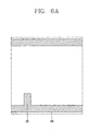
- FIGS. 6A to 6F are plan views sequentially showing a process of fabricating an array substrate illustrated in FIG. 4 according to an embodiment of the invention.
- FIGS. 7A to 7G are sectional views sequentially showing a process of fabricating an oxide TFT illustrated in FIG. 5 according to an embodiment of the invention.
- FIG. 8 is another sectional view schematically showing a structure of an oxide thin film transistor (TFT) according to an embodiment of the invention.
- TFT oxide thin film transistor
- FIGS. 9 and 10 are graphs showing transfer characteristics of the oxide TFT.
- TFT thin film transistor
- FIG. 4 is a plan view showing a portion of an array substrate of a liquid crystal display (LCD) device according to an embodiment of the invention.
- N number of gate lines and M number of data lines are formed to cross each other to define the M ⁇ N number of pixels in the LCD device, but in order to simplify the explanation, only a single pixel is shown in FIG. 4 .
- FIG. 5 is a sectional view schematically showing a structure of an oxide thin film transistor (TFT) according to an embodiment of the invention, which is taken along line A-A′ of the array substrate illustrated in FIG. 4 .
- AxByCzO AxByCzO
- a gate line 116 and a data line 117 are formed to be arranged vertically and horizontally to define a pixel region on an array substrate 110 .
- a thin film transistor (TFT), i.e., a switching element, is formed at a crossing of the gate line 116 and the data line 117 .
- a pixel electrode 118 is formed within the pixel region, is connected with the TFT to drive liquid crystal together with a common electrode of a color filter substrate.
- the oxide TFT includes a gate electrode 121 formed on the array substrate 110 , a gate insulating film 115 a formed on the gate electrode 121 , an active layer 124 made of an oxide semiconductor and formed at an upper side of the gate electrode 121 , first and second etch stoppers 125 a and 125 b made of a certain insulating material, and source and drain electrodes 122 and 123 electrically connected with source and drain regions of the active layer 124 .
- the oxide TFT according to an embodiment of the invention includes a protective layer 115 b formed on the array substrate 110 having the source and drain electrodes 122 and 123 formed thereon, and a pixel electrode 118 electrically connected with the drain electrode 123 through a contact hole 140 formed in the protective layer 115 b.
- the gate electrode 121 is connected with the gate line 116 , and a portion of the source electrode 122 extends in one direction so as to be connected with the data line 117 , and as mentioned above, the gate line 116 and the data line 117 are arranged vertically (or a first direction) and horizontally (or a second direction) on the array substrate 110 to define a pixel region.
- the oxide TFT employing the oxide semiconductor as the active layer 124 has high mobility and can be fabricated at a low temperature, and thus, the oxide TFT can be used in a transparent electronic circuit.
- the oxide semiconductor has a wide band gap, so it can be used in fabricating a UV LED, a white LED and any other components having high color purity, and also, since the oxide semiconductor can be processed at a low temperature, it may be used in manufacturing a light and flexible product.
- the first etch stopper 125 a and a second etch stopper 125 b made of a certain insulating material are formed at an upper portion of a channel region of the active layer 124 , and in this instance, the first and second etch stoppers 125 a and 125 b serve to prevent carrier concentration of the channel region from being changed due to a plasma treatment in a follow-up process.
- the oxide TFT after the oxide semiconductor layer is deposited, the insulating layer is immediately deposited to form the first etch stopper 125 a , thus minimizing damage to the back channel of the active layer 124 due to a chemical material or UV during the process.
- the oxide semiconductor layer and the insulating layer are sequentially deposited to form the active layer 24 , and then, another insulating layer is deposited and patterned to form the first and second etch stoppers 125 a and 125 b . This will be described in detail through a method for fabricating an oxide TFT as follows.
- the active layer 124 and the second etch stopper 125 b are arranged in a crossing direction, and left and right regions of the active layer 124 , which are not covered by the first and second etch stoppers 125 a and 125 b but exposed, constitute source and drain regions forming contact regions with the source and drain electrodes 122 and 123 .
- first etch stopper 125 a the second etch stopper 125 b , and the active layer 124 have an island-like shape.
- the second etch stopper 125 b is patterned to substantially have the same width as that of the underlying first etch stopper 125 a.
- FIGS. 6A to 6F are plan views sequentially showing a process of fabricating an array substrate illustrated in FIG. 4 according to an embodiment of the invention.
- FIGS. 7A to 7G are sectional views sequentially showing a process of fabricating an oxide TFT illustrated in FIG. 5 according to an embodiment of the invention.
- FIG. 8 is another sectional view schematically showing a structure of an oxide thin film transistor (TFT) according to an embodiment of the invention, which is taken along line B-B′ of the array substrate illustrated in FIG. 4 .
- TFT oxide thin film transistor
- the gate electrode 121 and the gate line 116 are formed on the array substrate 110 made of a transparent insulating material.
- an oxide semiconductor applied to (or utilized for) the oxide TFT may be deposited at a low temperature, so a substrate, such as a plastic substrate, soda lime glass, or the like, which can be applicable at a low temperature process may be used.
- the oxide TFT since the oxide TFT has amorphous characteristics, it can be used for a substrate of a large scale display.
- the gate electrode 121 and the gate line 116 are formed by depositing a first conductive film on the entire surface of the array substrate 110 and then selectively patterning the same through photolithography.
- the first conductive film may be made of a low resistance opaque conductive material such as aluminum (Al), an aluminum alloy, tungsten (W), copper (Cu), nickel (Ni), chromium (Cr), molybdenum (Mo), a molybdenum alloy, titanium (Ti), platinum (Pt), tantalum (Ta), or the like.
- the first conductive film may be made of a transparent conductive material such as indium tin oxide (ITO), indium zinc oxide (IZO), or the like, and may have a multilayered structure in which two or more conductive materials are stacked.
- the gate insulating layer 115 a , the oxide semiconductor layer 120 formed of a certain oxide semiconductor, and the first insulating layer 125 made of a certain insulating material are sequentially formed on the entire surface of the array substrate 110 having the gate electrode 121 and the gate line 116 formed thereon.
- an inorganic insulating film such as a silicon nitride film (SiNx), silicon oxide film (SiO 2 ), or the like, or a high dielectric oxide film such as hafnium (Hf) oxide or aluminum oxide may be used as the gate insulating film 115 a , and a silicon oxide film may be used as the first insulating layer 125 .
- the gate insulating film 115 a and the first insulating layer 125 may be formed through chemical vapor deposition (CVD) such as plasma enhanced chemical vapor deposition (PECVD), or physical vapor deposition (PVD) such as sputtering, or the like.
- CVD chemical vapor deposition
- PECVD plasma enhanced chemical vapor deposition
- PVD physical vapor deposition
- the active layer 124 formed of oxide semiconductor is formed at an upper side of the gate electrode 121 of the array substrate 110 .
- an insulating layer pattern 125 ′ made of the insulating material and patterned to have the substantially same shape as the active layer 124 is formed on the active layer 124 .
- the first insulating layer 125 may be etched by using dry etching such as oxygen plasma etching, and since the insulating layer pattern 125 ′ is patterned to have substantially the same shape as the underlying active layer 124 , the entire area of the underlying oxide semiconductor layer, namely, the active layer 124 , is prevented from being exposed, whereby instability due to the otherwise exposure can be removed and damage due to the patterning of the insulating layer pattern 125 ′ can be prevented.
- dry etching such as oxygen plasma etching
- the exposed side wall or side portions of the insulating layer pattern 125 ′ and the active layer 124 are portions having surfaces that are essentially perpendicular to the array substrate 110 . Further, the surfaces of the exposed side wall or side portions of the insulating layer pattern 125 ′ and the active layer 124 also extend from the source region to the drain region of the active layer. Accordingly, the surfaces of the exposed side wall or side portions of the insulating layer pattern 125 ′ and the active layer 124 are also essentially parallel to the array substrate 110 .
- a second insulating layer made of a certain insulating material is deposited on the entire surface of the array substrate 110 having the active layer 124 and the insulating layer pattern 125 ′ formed thereon, including the exposed side wall or side portions of the insulating layer pattern 125 ′ and the active layer 124 , and then, the insulating layer pattern 125 ′ and the second insulating layer are selectively patterned through photolithography.
- the first etch stopper 125 a and the second etch stopper 125 b are sequentially formed on the active layer 124 , excluding the left and right regions of the active layer 124 , namely, excluding the source and drain regions. Further, the second etch stopper 125 b is formed so that a portion of the second etch stopper 125 b covers the side walls or the side portions of the active layer 124 and the first etch stopper 125 a.
- an inorganic insulating film such as a silicon oxide film, a silicon nitride film or a high dielectric oxide film such as hafnium oxide or aluminum oxide may be used.
- the active layer 124 and the second etch stopper 125 b are arranged to be perpendicular. That is, the second etch stopper 125 b extends perpendicularly relative to the active layer 124 , when the second etch stopper 125 b and the active layer 124 are both parallel to the array substrate 110 .
- the first etch stopper 125 a , the second etch stopper 125 b , and the active layer 124 are formed as an island, and the second etch stopper 125 b is patterned to have substantially the same width as that of the first etch stopper 125 a.
- the source and drain regions of the active layer 124 form contact areas with the source and drain electrodes as resistance is reduced by an oxygen plasma treatment when the insulating layer pattern and the second insulating layer are etched through the oxygen plasma treatment to form the first etch stopper 125 a and the second etch stopper 125 b .
- the source and drain regions, contact regions may be formed by reducing resistance of the active layer 124 exposed through a thermal treatment or a surface treatment such as the oxygen plasma treatment after the first etch stopper 125 a and the second etch stopper 125 b are formed.
- the instance in which the active layer 124 is arranged to be perpendicular to the gate electrode 121 is described as an example, but the embodiments of the invention are not limited thereto, and the active layer 124 may be patterned to be arranged in the same direction as that of the gate electrode 121 , and in this instance, the second etch stopper 125 b may be patterned to be perpendicular to the underlying active layer 124 , i.e., the gate electrode 121 .
- the gate insulating film 115 a , the oxide semiconductor layer, and the first insulating layer are sequentially deposited to form the active layer 124 , and the second insulating layer is deposited and patterned to form the first etch stopper 125 a and the second etch stopper 125 b , whereby an exposure of the back channel region of the active layer 124 can be prevented, instability due to an exposure can be eliminated, and a loss of the gate insulating film 115 a can be prevented.
- a second conductive film is formed on the entire surface of the array substrate 110 having the active layer 124 , the first etch stopper 125 a , and the second etch stopper 125 b formed thereon.
- the second conductive film may be made of a low-resistance opaque conductive material such as aluminum (Al), an aluminum alloy, tungsten (W), copper (Cu), nickel (Ni), chromium (Cr), molybdenum (Mo), a molybdenum alloy, titanium (Ti), platinum (Pt), tantalum (Ta), or the like.
- the second conductive film may be made of transparent material such as ITO, IZO, or the like, or may be formed to have a multi-layered structure in which two or more conductive materials are stacked.
- the second conductive film is selectively patterned through photolithography to form the source electrode 122 and the drain electrode 123 electrically connected with the source region and the drain region of the active layer 124 , respectively.
- the protective film 115 b is formed on the entire surface of the array substrate 110 having the source and drain electrodes 122 and 123 formed thereon, and then selectively removed through photolithography to form the contact hole 140 exposing a portion of the drain electrode 123 on the array substrate 110 .
- a third conductive film is formed on the entire surface of the array substrate 110 having the protective film 115 b formed thereon and selectively removed through photolithography to from the pixel electrode 118 formed of the third conductive film on the array substrate 110 and electrically connected with the drain electrode 123 through the contact hole 140 .
- the third conductive film may be made of a transparent conductive material having excellent transmittance, such as ITO or IZO in order to form the pixel electrode 118 .
- FIG. 8 shows the second etch stopper 125 b being formed so that a portion of the second etch stopper 125 b covers the side walls or the side portions of the active layer 124 and the first etch stopper 125 a , when the side walls or the side portions of the active layer 124 and the first etch stopper 125 a are both perpendicular and parallel to the array substrate 110 .
- FIGS. 9 and 10 are graphs showing transfer characteristics of the oxide TFT.
- FIG. 9 shows transfer characteristics of a typical oxide TFT
- FIG. 10 shows transfer characteristics of the oxide TFT according to an embodiment of the invention.
- FIGS. 9 and 10 show the results obtained by measuring transfer characteristics of the respective oxide TFT at an initial state (INI) and a state (FIN) in which stress is applied.
- the stress test applies a negative bias of ⁇ 30V to a gate voltage. Namely, the negative bias was applied for one hour under backlight irradiation of 5000 unit at 60° C.
- the typical oxide TFT has a gentler slope of a transfer curve and lower on-current than those of the oxide TFT according to an embodiment of the invention, and its element characteristics are degraded by the stress test.
- the reason for this is because the back channel region of the active layer has been damaged to a degree by the photolithography for forming the active layer and the etch stopper.
- the oxide TFT according to an embodiment of the invention has a steep slope of the transfer curve and improved on-current, so it is noted that the transfer characteristics were improved and the element characteristics were not degraded by the stress test.
- the invention may also be used in a different display device fabricated by using TFTs as well as the LCD device, for example, an organic electroluminescent display device in which an organic electroluminescent element is connected to a driving transistor.
- the embodiments of the invention can be advantageously used for a transparent electronic circuit or a flexible display.
- the embodiments of the invention are not limited thereto. That is, the active layer may be formed of any oxide semiconductor.
Applications Claiming Priority (2)
| Application Number | Priority Date | Filing Date | Title |
|---|---|---|---|
| KR10-2010-0127171 | 2010-12-13 | ||
| KR1020100127171A KR20120065854A (ko) | 2010-12-13 | 2010-12-13 | 산화물 박막 트랜지스터의 제조방법 |
Publications (2)
| Publication Number | Publication Date |
|---|---|
| US20120146017A1 US20120146017A1 (en) | 2012-06-14 |
| US8735883B2 true US8735883B2 (en) | 2014-05-27 |
Family
ID=46198420
Family Applications (1)
| Application Number | Title | Priority Date | Filing Date |
|---|---|---|---|
| US13/324,751 Active US8735883B2 (en) | 2010-12-13 | 2011-12-13 | Oxide thin film transistor and method of fabricating the same |
Country Status (3)
| Country | Link |
|---|---|
| US (1) | US8735883B2 (ko) |
| KR (1) | KR20120065854A (ko) |
| CN (1) | CN102543754A (ko) |
Cited By (3)
| Publication number | Priority date | Publication date | Assignee | Title |
|---|---|---|---|---|
| US20130320328A1 (en) * | 2012-06-04 | 2013-12-05 | Samsung Display Co., Ltd. | Thin film transistor, thin film transistor array panel including the same, and manufacturing method thereof |
| US9905702B2 (en) | 2011-09-29 | 2018-02-27 | Semiconductor Energy Laboratory Co., Ltd. | Semiconductor device and method for manufacturing the same |
| US20200105798A1 (en) * | 2018-09-27 | 2020-04-02 | HKC Corporation Limited | Array substrate and display panel |
Families Citing this family (11)
| Publication number | Priority date | Publication date | Assignee | Title |
|---|---|---|---|---|
| CN103178021B (zh) * | 2013-02-28 | 2015-02-11 | 京东方科技集团股份有限公司 | 一种氧化物薄膜晶体管阵列基板及制作方法、显示面板 |
| KR102089313B1 (ko) * | 2013-04-30 | 2020-03-16 | 엘지디스플레이 주식회사 | 산화물 박막 트랜지스터 및 이의 제조 방법 |
| KR102148957B1 (ko) | 2013-09-02 | 2020-08-31 | 삼성디스플레이 주식회사 | 표시 기판 및 표시 기판의 제조 방법 |
| TW201515234A (zh) * | 2013-10-11 | 2015-04-16 | E Ink Holdings Inc | 主動元件及其製作方法 |
| KR102230301B1 (ko) | 2014-01-06 | 2021-03-22 | 삼성디스플레이 주식회사 | 박막 트랜지스터 및 그 제조 방법 |
| CN103915379B (zh) * | 2014-03-24 | 2017-07-04 | 京东方科技集团股份有限公司 | 一种氧化物薄膜晶体管阵列基板的制造方法 |
| TWI563669B (en) * | 2014-08-04 | 2016-12-21 | Innolux Corp | Thin film transistor and display panel using the same |
| CN104347643B (zh) * | 2014-09-04 | 2017-07-28 | 上海天马微电子有限公司 | 驱动电路及其形成方法、有机发光显示装置及其形成方法 |
| CN105914150A (zh) | 2016-04-29 | 2016-08-31 | 京东方科技集团股份有限公司 | 薄膜晶体管及制备方法、阵列基板及制备方法、显示面板、显示装置 |
| CN113345924A (zh) * | 2021-06-03 | 2021-09-03 | 京东方科技集团股份有限公司 | 显示面板及其制作方法和显示装置 |
| CN114709173A (zh) * | 2022-03-30 | 2022-07-05 | 广州华星光电半导体显示技术有限公司 | 阵列基板及其制备方法、显示面板 |
Citations (4)
| Publication number | Priority date | Publication date | Assignee | Title |
|---|---|---|---|---|
| US7110058B2 (en) * | 2002-10-25 | 2006-09-19 | Nec Lcd Technologies | Method of fabricating liquid crystal display device |
| WO2009136645A2 (en) | 2008-05-07 | 2009-11-12 | Canon Kabushiki Kaisha | Thin film transistor and method of manufacturing the same |
| CN101582453A (zh) | 2008-05-15 | 2009-11-18 | 三星电子株式会社 | 晶体管、半导体器件和制造晶体管、半导体器件的方法 |
| CN101794823A (zh) | 2009-02-04 | 2010-08-04 | 索尼公司 | 薄膜晶体管和显示装置 |
-
2010
- 2010-12-13 KR KR1020100127171A patent/KR20120065854A/ko not_active Application Discontinuation
-
2011
- 2011-12-12 CN CN2011104625450A patent/CN102543754A/zh active Pending
- 2011-12-13 US US13/324,751 patent/US8735883B2/en active Active
Patent Citations (7)
| Publication number | Priority date | Publication date | Assignee | Title |
|---|---|---|---|---|
| US7110058B2 (en) * | 2002-10-25 | 2006-09-19 | Nec Lcd Technologies | Method of fabricating liquid crystal display device |
| WO2009136645A2 (en) | 2008-05-07 | 2009-11-12 | Canon Kabushiki Kaisha | Thin film transistor and method of manufacturing the same |
| US20110042670A1 (en) * | 2008-05-07 | 2011-02-24 | Canon Kabushiki Kaisha | Thin film transistor and method of manufacturing the same |
| CN101582453A (zh) | 2008-05-15 | 2009-11-18 | 三星电子株式会社 | 晶体管、半导体器件和制造晶体管、半导体器件的方法 |
| CN101794823A (zh) | 2009-02-04 | 2010-08-04 | 索尼公司 | 薄膜晶体管和显示装置 |
| US20100193772A1 (en) | 2009-02-04 | 2010-08-05 | Sony Corporation | Thin film transistor and display device |
| US8426851B2 (en) * | 2009-02-04 | 2013-04-23 | Sony Corporation | Thin film transistor and display device |
Cited By (9)
| Publication number | Priority date | Publication date | Assignee | Title |
|---|---|---|---|---|
| US9905702B2 (en) | 2011-09-29 | 2018-02-27 | Semiconductor Energy Laboratory Co., Ltd. | Semiconductor device and method for manufacturing the same |
| US20130320328A1 (en) * | 2012-06-04 | 2013-12-05 | Samsung Display Co., Ltd. | Thin film transistor, thin film transistor array panel including the same, and manufacturing method thereof |
| US9093540B2 (en) * | 2012-06-04 | 2015-07-28 | Samsung Display Co., Ltd. | Oxide semicondutor thin film transistor |
| US9455333B2 (en) | 2012-06-04 | 2016-09-27 | Samsung Display Co., Ltd. | Thin film transistor array panel |
| US9793377B2 (en) | 2012-06-04 | 2017-10-17 | Samsung Display Co., Ltd. | Thin film transistor, thin film transistor array panel including the same, and manufacturing method thereof |
| USRE48290E1 (en) | 2012-06-04 | 2020-10-27 | Samsung Display Co., Ltd. | Thin film transistor array panel |
| US20200105798A1 (en) * | 2018-09-27 | 2020-04-02 | HKC Corporation Limited | Array substrate and display panel |
| US10854637B2 (en) * | 2018-09-27 | 2020-12-01 | HKC Corporation Limited | Array substrate and display panel |
| US11488982B2 (en) * | 2018-09-27 | 2022-11-01 | HKC Corporation Limited | Display panel and organic light emitting display panel |
Also Published As
| Publication number | Publication date |
|---|---|
| KR20120065854A (ko) | 2012-06-21 |
| US20120146017A1 (en) | 2012-06-14 |
| CN102543754A (zh) | 2012-07-04 |
Similar Documents
| Publication | Publication Date | Title |
|---|---|---|
| US8735883B2 (en) | Oxide thin film transistor and method of fabricating the same | |
| US10256344B2 (en) | Oxide thin film transistor and method of fabricating the same | |
| US7981720B2 (en) | Method of making thin film transistor with zinc oxide based semiconductor layer and zinc oxide based insulation layer | |
| KR101218090B1 (ko) | 산화물 박막 트랜지스터 및 그 제조방법 | |
| US8878181B2 (en) | Oxide thin film transistor and method of fabricating the same | |
| US9059296B2 (en) | Oxide thin film transistor and method of fabricating the same | |
| US8324111B2 (en) | Liquid crystal display device and method for fabricating the same | |
| KR101658533B1 (ko) | 산화물 박막 트랜지스터 및 그 제조방법 | |
| KR101622733B1 (ko) | 산화물 박막 트랜지스터의 제조방법 | |
| KR101697586B1 (ko) | 산화물 박막 트랜지스터 및 그 제조방법 | |
| KR101545923B1 (ko) | 산화물 박막 트랜지스터 및 그 제조방법 | |
| KR101640812B1 (ko) | 산화물 박막 트랜지스터의 제조방법 | |
| KR101605723B1 (ko) | 산화물 박막 트랜지스터의 제조방법 | |
| KR102039424B1 (ko) | 산화물 박막 트랜지스터의 제조방법 | |
| KR101616368B1 (ko) | 산화물 박막 트랜지스터의 제조방법 | |
| KR101298611B1 (ko) | 산화물 박막 트랜지스터 및 그 제조방법 | |
| KR101875940B1 (ko) | 산화물 박막 트랜지스터 및 그 제조방법 | |
| KR20120075110A (ko) | 산화물 박막 트랜지스터의 제조방법 | |
| KR101487256B1 (ko) | 산화물 박막 트랜지스터의 제조방법 | |
| KR20110070561A (ko) | 비정질 산화물 박막 트랜지스터 및 그 제조방법 |
Legal Events
| Date | Code | Title | Description |
|---|---|---|---|
| AS | Assignment |
Owner name: LG DISPLAY CO., LTD., KOREA, REPUBLIC OF Free format text: ASSIGNMENT OF ASSIGNORS INTEREST;ASSIGNORS:KIM, DAE-HWAN;CHOI, BYUNG-KOOK;LEE, SUL;AND OTHERS;REEL/FRAME:027534/0375 Effective date: 20111212 |
|
| STCF | Information on status: patent grant |
Free format text: PATENTED CASE |
|
| FEPP | Fee payment procedure |
Free format text: PAYOR NUMBER ASSIGNED (ORIGINAL EVENT CODE: ASPN); ENTITY STATUS OF PATENT OWNER: LARGE ENTITY |
|
| MAFP | Maintenance fee payment |
Free format text: PAYMENT OF MAINTENANCE FEE, 4TH YEAR, LARGE ENTITY (ORIGINAL EVENT CODE: M1551) Year of fee payment: 4 |
|
| MAFP | Maintenance fee payment |
Free format text: PAYMENT OF MAINTENANCE FEE, 8TH YEAR, LARGE ENTITY (ORIGINAL EVENT CODE: M1552); ENTITY STATUS OF PATENT OWNER: LARGE ENTITY Year of fee payment: 8 |