US8711579B2 - Switching power supply apparatus with overcurrent limiting and prolonged holding time - Google Patents
Switching power supply apparatus with overcurrent limiting and prolonged holding time Download PDFInfo
- Publication number
- US8711579B2 US8711579B2 US13/180,728 US201113180728A US8711579B2 US 8711579 B2 US8711579 B2 US 8711579B2 US 201113180728 A US201113180728 A US 201113180728A US 8711579 B2 US8711579 B2 US 8711579B2
- Authority
- US
- United States
- Prior art keywords
- voltage
- converter
- current
- input voltage
- threshold
- Prior art date
- Legal status (The legal status is an assumption and is not a legal conclusion. Google has not performed a legal analysis and makes no representation as to the accuracy of the status listed.)
- Expired - Fee Related, expires
Links
Images


Classifications
-
- H—ELECTRICITY
- H02—GENERATION; CONVERSION OR DISTRIBUTION OF ELECTRIC POWER
- H02M—APPARATUS FOR CONVERSION BETWEEN AC AND AC, BETWEEN AC AND DC, OR BETWEEN DC AND DC, AND FOR USE WITH MAINS OR SIMILAR POWER SUPPLY SYSTEMS; CONVERSION OF DC OR AC INPUT POWER INTO SURGE OUTPUT POWER; CONTROL OR REGULATION THEREOF
- H02M3/00—Conversion of dc power input into dc power output
- H02M3/22—Conversion of dc power input into dc power output with intermediate conversion into ac
- H02M3/24—Conversion of dc power input into dc power output with intermediate conversion into ac by static converters
- H02M3/28—Conversion of dc power input into dc power output with intermediate conversion into ac by static converters using discharge tubes with control electrode or semiconductor devices with control electrode to produce the intermediate ac
- H02M3/325—Conversion of dc power input into dc power output with intermediate conversion into ac by static converters using discharge tubes with control electrode or semiconductor devices with control electrode to produce the intermediate ac using devices of a triode or a transistor type requiring continuous application of a control signal
- H02M3/335—Conversion of dc power input into dc power output with intermediate conversion into ac by static converters using discharge tubes with control electrode or semiconductor devices with control electrode to produce the intermediate ac using devices of a triode or a transistor type requiring continuous application of a control signal using semiconductor devices only
- H02M3/33507—Conversion of dc power input into dc power output with intermediate conversion into ac by static converters using discharge tubes with control electrode or semiconductor devices with control electrode to produce the intermediate ac using devices of a triode or a transistor type requiring continuous application of a control signal using semiconductor devices only with automatic control of the output voltage or current, e.g. flyback converters
-
- H—ELECTRICITY
- H02—GENERATION; CONVERSION OR DISTRIBUTION OF ELECTRIC POWER
- H02M—APPARATUS FOR CONVERSION BETWEEN AC AND AC, BETWEEN AC AND DC, OR BETWEEN DC AND DC, AND FOR USE WITH MAINS OR SIMILAR POWER SUPPLY SYSTEMS; CONVERSION OF DC OR AC INPUT POWER INTO SURGE OUTPUT POWER; CONTROL OR REGULATION THEREOF
- H02M1/00—Details of apparatus for conversion
- H02M1/32—Means for protecting converters other than automatic disconnection
-
- H—ELECTRICITY
- H02—GENERATION; CONVERSION OR DISTRIBUTION OF ELECTRIC POWER
- H02M—APPARATUS FOR CONVERSION BETWEEN AC AND AC, BETWEEN AC AND DC, OR BETWEEN DC AND DC, AND FOR USE WITH MAINS OR SIMILAR POWER SUPPLY SYSTEMS; CONVERSION OF DC OR AC INPUT POWER INTO SURGE OUTPUT POWER; CONTROL OR REGULATION THEREOF
- H02M1/00—Details of apparatus for conversion
- H02M1/0003—Details of control, feedback or regulation circuits
- H02M1/0016—Control circuits providing compensation of output voltage deviations using feedforward of disturbance parameters
- H02M1/0022—Control circuits providing compensation of output voltage deviations using feedforward of disturbance parameters the disturbance parameters being input voltage fluctuations
-
- H—ELECTRICITY
- H02—GENERATION; CONVERSION OR DISTRIBUTION OF ELECTRIC POWER
- H02M—APPARATUS FOR CONVERSION BETWEEN AC AND AC, BETWEEN AC AND DC, OR BETWEEN DC AND DC, AND FOR USE WITH MAINS OR SIMILAR POWER SUPPLY SYSTEMS; CONVERSION OF DC OR AC INPUT POWER INTO SURGE OUTPUT POWER; CONTROL OR REGULATION THEREOF
- H02M1/00—Details of apparatus for conversion
- H02M1/32—Means for protecting converters other than automatic disconnection
- H02M1/325—Means for protecting converters other than automatic disconnection with means for allowing continuous operation despite a fault, i.e. fault tolerant converters
-
- Y—GENERAL TAGGING OF NEW TECHNOLOGICAL DEVELOPMENTS; GENERAL TAGGING OF CROSS-SECTIONAL TECHNOLOGIES SPANNING OVER SEVERAL SECTIONS OF THE IPC; TECHNICAL SUBJECTS COVERED BY FORMER USPC CROSS-REFERENCE ART COLLECTIONS [XRACs] AND DIGESTS
- Y02—TECHNOLOGIES OR APPLICATIONS FOR MITIGATION OR ADAPTATION AGAINST CLIMATE CHANGE
- Y02B—CLIMATE CHANGE MITIGATION TECHNOLOGIES RELATED TO BUILDINGS, e.g. HOUSING, HOUSE APPLIANCES OR RELATED END-USER APPLICATIONS
- Y02B70/00—Technologies for an efficient end-user side electric power management and consumption
- Y02B70/10—Technologies improving the efficiency by using switched-mode power supplies [SMPS], i.e. efficient power electronics conversion e.g. power factor correction or reduction of losses in power supplies or efficient standby modes
Definitions
- the present application relates, for example, to a switching power supply apparatus having a resonant switching converter.
- Switching power supply apparatuses equipped with a variety of resonant converters are widely used.
- a high power conversion efficiency can be easily achieved by a resonant converter, and a low noise characteristics can be also achieved because a switching waveform of the resonant converter is a substantially sinusoidal waveform.
- a resonant converter has an advantage of being configurable with a comparatively small number of components.
- a configuration employing a half-bridge coupling system in which a switching circuit composed of two switching elements serially connected is disposed in parallel with a DC input voltage, is widely used.
- the current resonant converter employing a half-bridge coupling system is configured such that two switching elements alternately turn ON/OFF.
- a combination of each switching element and a resonant capacitor connected in parallel with each other is commonly in use.
- Switching drive for a resonant converter is configured such that two switching elements alternately turn ON/OFF, and a transient period during which both switching elements are OFF at the same time is set. This transient period is set to prevent two switching elements from turning ON at the same time.
- FIG. 1 shows an example of a switching power supply circuit that uses a current resonant converter employing a half-bridge coupling system as a DC-DC converter 4 , where the half-bridge coupling system includes field-effect transistors (hereinafter referred to as FETs accordingly) Q 1 and Q 2 as switching elements.
- a commercial power supply is supplied to an AC/DC converter 3 via an AC plug 1 and a fuse 2 .
- the AC/DC converter 3 is composed of a diode bridge BD, and a DC voltage output from the AC/DC converter 3 is supplied to a blocking capacitor (smoothing capacitor) Ci.
- a voltage generated across the blocking capacitor Ci is supplied to the DC-DC converter 4 configured as a current resonant converter.
- a primary series resonant capacitor (hereinafter referred to as a resonant capacitor accordingly) C 1 is disposed between one end of a primary coil N 1 and the ground.
- the power supply apparatus shown in FIG. 1 employs the configuration to drive the switching elements by an external excitation.
- the DC-DC converter 4 shown in FIG. 1 includes a series connection circuit composed of one FET Q 1 and the other FET Q 2 .
- two FETs Q 1 and Q 2 are coupled in a half-bridge configuration.
- the half-bridge circuit composed of these FET Q 1 and FET Q 2 is connected in parallel with a DC input voltage Vdc across the blocking capacitor Ci. Because the FET Q 1 and FET Q 2 are switching-driven, the DC input voltage Vdc sent to the FET Q 1 and FET Q 2 is switched.
- a body diode D 1 is connected in a so-called antiparallel state with the FET Q 1 .
- the drain of the FET Q 1 is connected with the cathode of the body diode D 1
- the source of the FET Q 1 is connected with the anode of the body diode D 1 so that the forward direction of the FET Q 1 and the forward direction the body diode are reversed.
- a body diode D 2 is connected in an antiparallel state with the FET Q 2 .
- a series resonant circuit which is composed of a primary coil N 1 of a transformer T, a leakage inductance component L 1 of the transformer T, and a resonant capacitor C 1 , is connected in parallel with the FET Q 2 .
- a resonant capacitor is not connected with the FET Q 1 .
- a resonant operation of the configuration with a resonant capacitor connected in parallel with the FET Q 2 and without any resonant capacitor connected in parallel with the FET Q 1 is similar to that of the configuration with two resonant capacitors connected in parallel with the FET Q 1 and FET Q 2 respectively.
- a control circuit 9 is provided for switching-driving the FET Q 1 and FET Q 2 by an external excitation, and includes, for example, an oscillator 10 and a drive circuit 11 as shown in FIG. 1 .
- the oscillator 10 generates an oscillating signal with a predefined frequency, and supplies the oscillating signal to the drive circuit 11 .
- the drive circuit 11 generates drive signals SG 1 and SG 2 for switching-driving the FET Q 1 and FET Q 2 with the use of the input oscillating signal.
- the frequencies of these drive signals SG 1 and SG 2 are determined on the basis of the output signal of the oscillator 10 input to the drive circuit 11 .
- the control circuit 9 also includes an error amplifier 12 and a photocoupler 13 .
- the transformer T is provided for transmitting a switching output of the FET Q 1 and FET Q 2 from the primary side to the secondary side, and is fabricated by winding a primary coil N 1 and a secondary coil N 2 around a core.
- the leakage inductance component L 1 contributes to a resonant operation.
- One end part of the primary coil N 1 is connected with the connection node between the FET Q 1 and FET Q 2 , and the other end part is connected with the negative side of the DC input voltage Vdc via the series resonant capacitor C 1 .
- the leakage inductance component L 1 is connected in series with the resonant capacitor C 1 , and this series connection of L 1 and C 1 forms a primary side series resonant circuit.
- the switching output of the FET Q 1 and FET Q 2 is supplied to the primary side series resonant circuit, which makes the switching operation of the primary side series resonant circuit a current resonant operation.
- the center tap formed at the center point of the secondary coil N 2 is connected with the secondary side ground.
- rectifier diodes D 3 and D 4 , and a smoothing capacitor Co connected as shown in FIG. 1 form a secondary side full-wave rectifier.
- An alternating voltage excited on the secondary coil N 2 is rectified and smoothed by this secondary side full-wave rectifier.
- a secondary side DC voltage Vout is generated as a voltage across the smoothing capacitor Co, and supplied to a load.
- the secondary side DC voltage Vout is branched and supplied to the error amplifier 12 in the control circuit 9 .
- the level of the secondary side DC voltage Vout and the predefined level of a reference voltage Vref are compared with each other, and an error signal having the level corresponding to an error between two levels is generated and supplied to the oscillator 10 via a photocoupler 13 .
- the photocoupler 13 is provided for isolating the primary side from the secondary side in order to accurately feed back the error signal from the secondary side to the oscillator 10 that is supposed to be disposed on the primary side.
- a resistor Ro is disposed to adjust a current to be injected into a photodiode in the photocoupler 13 in accordance with the error signal.
- the oscillator 10 is a variable-frequency oscillator that changes its oscillating frequency in accordance with the error signal.
- the amount of energy transmitted from the primary side to the secondary side changes as the switching frequency of the FET Q 1 and FET Q 2 changes, with the result that the level of the secondary side DC voltage Vout is variably controlled.
- the secondary side DC output voltage can be stabilized by the above-described control system.
- the stabilization control works such that the switching frequency is made low when the level of the secondary side DC voltage Vout lowers. As a result, the amount of energy transmitted to the secondary side increases and the secondary side DC voltage Vout rises. When the level of the secondary side DC voltage Vout rises, the switching frequency is made high, with the result that the amount of energy transmitted to the secondary side decreases and the secondary side DC voltage Vout lowers.
- a pulse-width modulation circuit can be used to stabilize the output voltage by changing the pulse width of its output pulse.
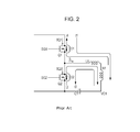
- FIG. 2 shows a circuit including the FET Q 1 and FET Q 2 as a part of the entire circuit shown in FIG. 1 .
- FIG. 3 shows the waveforms of the drive signals SG 1 and SG 2 , the waveforms of the currents IQ 1 , IQ 2 , and IL, and the waveform of the voltage VC 1 across the resonant capacitor C 1 at the time when the power supply for the switching power supply circuit is in a stable state (or when the switching power supply circuit is in a normal operation state).
- the currents IQ 1 and IQ 2 represent currents that flow through the FET Q 1 and FET Q 2 respectively
- the current IL represents a current that flows through the resonant circuit.
- the drive circuit 11 supplies the drive signals SG 1 and SG 2 to the gates of the FET Q 1 and FET Q 2 respectively as shown in FIG. 3A and FIG. 3B .
- the FET Q 1 is ON during the time period when the drive signal SG 1 is in the high level of a positive polar pulse, and the FET Q 1 is OFF during the time period when the drive signal SG 1 is in the low level. The same is equally true of the FET Q 2 and the drive signal SG 2 .
- the drive signal SG 1 is in the low level, so both FET Q 1 and FET Q 2 are OFF.
- the IQ 2 shown in FIG. 3D transiently flows through a route from D 2 , L 1 , and N 1 to C 1 in order to hold a resonant state formed by the leakage inductance component L 1 and the resonant capacitor C 1 .
- the FET Q 2 becomes ON.
- the current IQ 2 flows through a route from D 2 , L 1 , and N 1 to C 1 and a route from Q 2 , L 1 , and N 1 to C 1 .
- the current IQ 2 begins to flow reversely through a route from C 1 , N 1 , and L 1 to Q 2 over time.
- the time period t 4 is a transient time period, in which the drive signal SG 2 is in the low level, so the FET Q 2 is OFF. Because the FET Q 1 is also OFF, the IQ 1 flows through a route from C 1 , N 1 , and L 1 to Q 1 as shown in FIG. 3C . After the time period t 4 is over, the operation of the circuit again returns to that in the time period t 1 .
- the above-described switching power supply circuit is equipped with an overcurrent limiting circuit for protecting a power supply circuit or a load circuit.
- the overcurrent limiting circuit stops the operation of the converter circuit.
- FIG. 4 shows an example of a switching power supply circuit equipped with an overcurrent limiting circuit.
- the leakage inductance component L 1 , the output side smoothing capacitor Co, the load, the feedback loop, and the like in FIG. 1 are not shown in FIG. 4 .
- the overcurrent limiting circuit 6 includes a comparator 6 a.
- a current that flows the primary side of the transformer T is detected at a current detecting point 5 , for example, as a voltage.
- the obtained voltage is sent to the comparator 6 a , and is compared with the voltage value of a DC voltage supply 6 b .
- the detected voltage exceeds the voltage value of the DC voltage supply 6 b , and the polarity of the output of the comparator 6 a is reversed.
- the operation of the DC-DC converter 4 is stopped by the output of the comparator 6 a .
- the switching operation of the FET Q 1 and FET Q 2 is stopped. As a result, the output power supply to the load is cut off.
- the time during which the power supply circuit can continue to supply power after the input to the power supply circuit is cut off is called a holding time.
- the technique disclosed in Japanese Unexamined Patent Application Publication 07-312861 is used for holding the output voltage of a switching power supply apparatus in a normal operation constant, and its primary objective is to deduce the power consumption of an input voltage detecting circuit.
- a primary objective of the technique disclosed in Japanese Unexamined Patent Application Publication 2004-166440 is to make full use of the capability of a power factor improvement circuit.
- a primary objective of the technique disclosed in Japanese Unexamined Patent Application Publication 2002-51540 is to improve efficiency. Therefore, it is difficult to prolong a holding time with the use of the contents disclosed in these unexamined patent application publications.
- a switching power supply apparatus that can prolong the holding time even if the apparatus is equipped with an overcurrent limiting circuit.
- a switching power supply apparatus includes: a switching DC-DC converter for receiving an input voltage; a current detecting unit for detecting a current from the DC-DC converter; an input voltage detecting unit for detecting the decrease or cutoff of the input voltage; an overcurrent limiting circuit for stopping the operation of the DC-DC converter when the current detected by the current detecting unit exceeds a threshold; and a threshold control unit for changing the threshold of the overcurrent limiting circuit such that, if the decrease or cutoff of the input voltage is detected by the input voltage detecting unit, the period between the time when the decrease or cutoff of the input voltage is detected and the time when the operation of the DC-DC converter is stopped is prolonged.
- a first embodiment further includes an AC/DC converter in front of the DC-DC converter, in which the input voltage detecting unit detects the decrease or cutoff of an AC voltage supplied to the AC/DC converter.
- a second embodiment further includes a smoothing capacitor in front of the DC-DC converter, in which the input voltage detecting unit detects the decrease or cutoff of a terminal voltage across the smoothing capacitor.
- the holding time can be prolonged, thereby a load circuit can perform termination processing at an easier pace.
- FIG. 1 is a circuit diagram showing the configuration of an existing switching power supply apparatus
- FIG. 2 is a circuit diagram used for describing the operation of the existing switching power supply apparatus
- FIG. 3A to FIG. 3F are waveform charts showing signal waveforms of several parts of the existing switching power supply apparatus when the apparatus is in operation;
- FIG. 4 is a circuit diagram used for describing an overcurrent limiting circuit of the existing switching power supply apparatus
- FIG. 5A and FIG. 5B are conceptual diagrams showing advantages and disadvantages between the existing apparatus and an apparatus according to the present application in comparison;
- FIG. 6 is a conceptual diagram showing an example of threshold control
- FIG. 7 is a conceptual diagram showing another example of threshold control
- FIG. 8 is a circuit diagram showing a first example of a first embodiment
- FIG. 9 is a circuit diagram showing a second example of the first embodiment.
- FIG. 10 is a circuit diagram showing a third example of the first embodiment
- FIG. 11 is a circuit diagram showing a first example of a second embodiment
- FIG. 12 is a circuit diagram showing a second example of the second embodiment
- FIG. 13 is a circuit diagram showing a third example of the second embodiment
- FIG. 14 is a circuit diagram showing a first example of a third embodiment
- FIG. 15 is a circuit diagram showing a second example of the third embodiment.
- FIG. 16 is a circuit diagram showing a third example of the third embodiment.
- the apparatus detects the decrease or cutoff of an input voltage through directly monitoring the input voltage or through detecting the decrease of a voltage across a blocking capacitor, and changes a threshold, which is used when an overcurrent limiting circuit operates, within a range where the operations of circuits of the apparatus and a load are not adversely affected by changing the threshold.
- a threshold which is used when an overcurrent limiting circuit operates, within a range where the operations of circuits of the apparatus and a load are not adversely affected by changing the threshold.
- FIG. 5A shows the operation of an existing apparatus equipped with an existing overcurrent limiting circuit
- FIG. 5B shows the operation of an embodiment according to the present application.
- a voltage change a shows a terminal voltage across the blocking capacitor Ci, that is, the input voltage to the DC-DC converter 4
- b represents an operating voltage range
- c represents a time at which the input voltage is cut off
- d represents a limiting time until which the output voltage is held
- e represents the change of a current that flows the primary side of the transformer T
- f represents the overcurrent threshold
- g represents the output voltage.
- FIG. 5A shows the envelope of the current.
- a, b′, c, d′, e′, f, and g′ are respectively the counterparts of a, b, c, d, e, f, and g in FIG. 5A .
- a voltage change and a time at which the input voltage is cut off in FIG. 5B is the same as those in FIG. 5A , thereby the same alphabets are given.
- the overcurrent threshold f is set to be higher than f at the time c at which the input voltage is cut off.
- the time at which the current e′ becomes larger than the threshold f becomes d′.
- a voltage range within which the apparatus according to this embodiment can be in operation is enlarged from b to b′, thereby the holding time of output becomes the difference between the time c and the time d′.
- the difference between the time c and the time d′ is larger than the difference between the time c and the time d, thereby the holding time of output is enlarged in this embodiment.
- the size of circuit components for the overcurrent limiting circuit used in the apparatus according to the embodiment is small, thereby these components can be easily added to an existing integrated circuit.
- the holding time can be prolonged, the capacity of the blocking capacitor can be made small. Because a small-sized capacitor with a small capacity can be used as the blocking capacitor, mechanical limitation on the design of a power supply circuit is alleviated, with the result that the power supply circuit can be downsized.
- the threshold can be changed not only stepwise, but also in a curved line as shown in FIG. 6 .
- the output power is constant
- the relationship between a capacitor voltage (in the x-axis) and a current (in the y-axis) is shown by a curve o in FIG. 6 .
- an overcurrent threshold p used in the existing apparatus is constant, overcurrent limiting operation works at a point where the current exceeds the threshold p (shown by q). Therefore, the existing apparatus does not operates with the capacitor voltage equal to or smaller than the voltage value corresponding to this point.
- the threshold r in a curved line in accordance with the current o it can be realized to make the current not to exceed the threshold r in a range within which the existing apparatus can normally operate.
- FIG. 7 shows a configuration that the threshold is changed in two steps.
- the overcurrent threshold used in the existing apparatus is constant as shown by p.
- a threshold r′ which is changed in two steps such that its value is high within a range where the capacitor voltage is low, and low within a range where the capacitor voltage is high, is used in the apparatus according to the embodiment.
- a switching power supply apparatus detects the decrease or cutoff of an input voltage, and changes a threshold, which is used when an overcurrent limiting circuit operates, within a range where the operations of circuits of the apparatus and a load are not adversely affected by changing the threshold.
- a threshold which is used when an overcurrent limiting circuit operates, within a range where the operations of circuits of the apparatus and a load are not adversely affected by changing the threshold.
- FIG. 8 shows a first example of the overcurrent limiting circuit according to the input voltage detecting method.
- the configuration shown in FIG. 8 is the same as that shown in FIG. 4 except for the configuration of an overcurrent limiting circuit 61 .
- an AC voltage on the input side of an AC/DC converter 3 is supplied to the anode of a diode 7 a , and the cathode of the diode 7 a is connected with the ground via resisters 7 b and 7 c .
- a capacitor 7 d is connected in parallel with the resister 7 c .
- the rectified voltage of the input AC voltage is generated at the connection node between a resistor 7 b and a resistor 7 c.
- the rectified voltage is supplied to a comparator 7 e , and is compared with a DC voltage source 7 f (a threshold 7 f ) by the comparator 7 e .
- the output of the comparator 7 e becomes at a high level (“at a high level” will be hereinafter abbreviated to “H” accordingly) when a voltage applied to the (+) input (hereinafter referred to as Vin+) of the comparator 7 e is larger than a voltage applied to the ( ⁇ ) input (hereinafter referred to as Vin ⁇ ) of the comparator 7 e , and becomes at a low level (“at a low level” will be hereinafter abbreviated to “L” accordingly) when Vin ⁇ is larger than Vin+.
- Vin ⁇ of the comparator 7 e is larger than Vin+, therefore the output becomes L.
- the output voltage of the comparator 7 e is supplied to the ( ⁇ ) input of a comparator 6 a via a resistor 6 d .
- a series circuit composed of a resistor 6 c and a DC voltage supply 6 b is connected between the ( ⁇ ) input of the comparator 6 a and the ground.
- a threshold determined by the DC voltage supply 6 b , the resister 6 c , and the resister 6 d is supplied to the ( ⁇ ) input of the comparator 6 a.
- the output of the comparator 6 a becomes H.
- the output of the comparator 6 a is supplied to an oscillator, a PMW modulator, and the like of a DC-DC converter 4 , and when the output of the comparator 6 a becomes H, the switching operation of FETs Q 1 and Q 2 is stopped. In other words, the operation of the DC-DC converter 4 is stopped and overcurrent limiting operation is performed.
- FIG. 9 shows a second example of the overcurrent limiting circuit according to the input voltage detecting method.
- the configuration shown in FIG. 9 is the same as that shown in FIG. 4 except for the configuration of an overcurrent limiting circuit 62 .
- the rectified output of an AC voltage on the input side of the AC/DC converter 3 is sent to the base of an NPN transistor 16 via a resistor 15 .
- the emitter of the transistor 16 is earthed, and the collector of the transistor 16 is connected with a positive DC voltage supply line via a resistor 17 .
- the collector of the transistor 16 is connected with the base of an NPN transistor 19 via a resistor 18 .
- the emitter of the transistor 19 is earthed, and the collector of the transistor 19 is connected with the connection node between a resistor 21 and a resistor 22 via a resistor 20 .
- a series circuit of the resistor 21 and the resistor 22 is disposed between a current detecting point 5 and the ground.
- a voltage generated at the connection node between the resistor 21 and the resistor 22 is supplied to a reference terminal of a shut regulator 23 .
- the anode of the shunt regulator 23 is earthed, and the cathode of the shunt regulator 23 is connected with a positive DC voltage supply line via a resistor 24 .
- the cathode of the shunt regulator 23 is connected with the base of an NPN transistor 26 via a resistor 25 .
- the emitter of a transistor 26 is earthed, and the collector of the transistor 26 is connected with a positive DC voltage supply line via a resistor 27 .
- the operation of a DC-DC converter 4 is controlled by an output generated at the collector of the transistor 26 .
- the operation of a DC-DC converter 4 is controlled in such a way that, if the output of the transistor 26 is H, the operation of the DC-DC converter 4 is stopped.
- the transistor 16 In a normal operation state in which the input AC voltage is supplied, the transistor 16 is ON owing to the rectified output of the AC voltage, and the collector of the transistor 16 is L. Therefore the transistor 19 becomes OFF. Therefore, the connection node between the resistors 21 and 22 becomes in a state similar to that in which the connection node is not connected with the transistor 19 via the resistor 20 .
- a voltage obtained by dividing a voltage, which is obtained by converting a current detected at the current detecting point 5 , by the resistor 21 and resistor 22 is supplied to the reference terminal of the shunt regulator 23 .
- the voltage supplied to the reference terminal that is, the voltage at the connection node between the resistor 21 and resistor 22 , is compared with a reference voltage (equivalent to a threshold) embedded in the shunt regulator 23 , and a current corresponding to the difference between the above two voltages flows between the anode and the cathode of the shunt regulator 23 .
- the transistor 16 In a state in which the input voltage is neither decreased nor cut off, the transistor 16 is ON, and the transistor 19 is OFF, thereby the connection node between the resistors 21 and 22 becomes in a state similar to that in which the transistor 19 is not connected.
- the transistor 16 if the input voltage is decreased or cut off, the transistor 16 becomes OFF, and the transistor 19 becomes ON, thereby the resistor 20 is equivalently connected in parallel with the resistor 22 .
- the resistor R 20 because a branch path is formed by the resistor R 20 , the voltage at the connection node between the resistor 21 and resistor 22 becomes lower.
- the input voltage to the shunt regulator 23 is lowered. This is equivalent to increasing the reference voltage (threshold) of the shunt regulator 23 . Therefore, if the decrease or cutoff of the input voltage is generated, the holding time can be prolonged.
- FIG. 10 shows a third example of the overcurrent limiting circuit according to the input voltage detecting method.
- the configuration shown in FIG. 10 is the same as that shown in FIG. 4 except for the configuration of an overcurrent limiting circuit 63 .
- the rectified output of an AC voltage on the input side of the AC/DC converter 3 is sent to the base of an NPN transistor 16 via a resistor 15 .
- the emitter of the transistor 16 is earthed, and the collector of the transistor 16 is connected with a positive DC voltage supply line via a resistor 17 .
- the collector of the transistor 16 is connected with the base of an NPN transistor 19 via a resistor 18 .
- the emitter of a transistor 19 is earthed.
- the third example of the overcurrent limiting circuit is equipped with a zener diode 32 .
- the cathode of the zener diode 32 is connected with a current detecting point 5
- the anode of the zener diode 32 is connected with the ground via a resistor 33 .
- the connection node between the resistor 31 and the cathode of the zener diode 32 is connected with the collector of the transistor via the resistor 20 .
- a control signal for controlling the operation of a DC-DC converter 4 is taken out from the connection node between the anode of the zener diode 32 and the resistor 33 .
- the transistor 16 In a normal operation state in which the input AC voltage is supplied, the transistor 16 is ON owing to the rectified output of the AC voltage, and the transistor 19 becomes OFF. Therefore, the connection node between the resistor 31 and the cathode of the zener diode 32 becomes in a state similar to that in which the connection node is not connected with the transistor 19 via the resistor 20 .
- the transistor 16 becomes OFF, and the transistor 19 becomes ON, thereby a branch path is formed by the resistor R 20 , and the voltage applied to the zener diode 32 is lowered.
- the input voltage to the zener diode 32 is lowered. This is equivalent to increasing the zener voltage (threshold) of the zener diode 32 . Therefore, if the decrease or cutoff of the input voltage is generated, the holding time can be prolonged.
- a switching power supply apparatus detects the decrease or cutoff of an input voltage by monitoring a voltage across a blocking capacitor, and changes a threshold, which is used when an overcurrent limiting circuit operates, within a range where the operations of circuits of the apparatus and a load are not adversely affected by changing the threshold.
- a threshold which is used when an overcurrent limiting circuit operates, within a range where the operations of circuits of the apparatus and a load are not adversely affected by changing the threshold.
- FIG. 11 shows a first example of the overcurrent limiting circuit according to the blocking capacitor voltage detecting method.
- FIG. 11 The configuration shown in FIG. 11 is the same as that shown in FIG. 4 except for the configuration of an overcurrent limiting circuit 64 .
- This example has a configuration corresponding to that of the above described first example of the input voltage detecting method (Refer to FIG. 8 ).
- One terminal of a blocking capacitor Ci is connected with the ground via resistors 8 a and 8 b .
- a voltage at the connection node between the resistors 8 a and 8 b is supplied to the ( ⁇ ) input of a comparator 8 c , and is compared with a DC voltage source 8 d (a threshold 8 d ) by a comparator 8 c .
- the output of the comparator 8 c becomes at a high level (“at a high level” will be hereinafter abbreviated to “H” accordingly) when Vin+ is larger than Vin ⁇ , and becomes at a low level (“at a low level” will be hereinafter abbreviated to “L” accordingly) when Vin ⁇ is larger than Vin+.
- Vin ⁇ of the comparator 8 c is larger than Vin+, therefore the output becomes L.
- the output voltage of the comparator 8 c is supplied to the ( ⁇ ) input of the comparator 6 via a resistor 6 d .
- a series circuit composed of a resistor 6 c and a threshold voltage 6 b (a DC voltage supply 6 b ) is connected between the ( ⁇ ) input of the comparator 6 a and the ground.
- a threshold determined by the DC voltage supply 6 b , the resister 6 c , and the resister 6 d is supplied to the ( ⁇ ) input of the comparator 6 a.
- the output of the comparator 6 a becomes H.
- the output of the comparator 6 a is supplied to an oscillator, a PMW modulator, and the like of a DC-DC converter 4 , and when the output of the comparator 6 a becomes H, the switching operation of FETs Q 1 and Q 2 is stopped. In other words, the operation of the DC-DC converter 4 is stopped and overcurrent limiting operation is performed.
- FIG. 12 shows a second example of the overcurrent limiting circuit according to the blocking capacitor voltage detecting method.
- the configuration shown in FIG. 12 is the same as that shown in FIG. 4 except for the configuration of an overcurrent limiting circuit 65 .
- This example has a configuration corresponding to that of the above described second example of the input voltage detecting method (Refer to FIG. 9 ).
- One terminal of a blocking capacitor Ci is connected with the ground via resistors 8 a and 8 b .
- a voltage at the connection node between the resistors 8 a and 8 b is supplied to the base of an NPN transistor 8 f
- the emitter of the transistor 8 f is earthed, and the collector of the transistor 8 f is connected with a positive DC voltage supply line via a resistor 8 g , and is also connected with the base of a transistor 19 via a resistor 18 .
- the emitter of the transistor 19 is earthed, and the collector of the transistor 19 is connected with the connection node between a resistor 21 and a resistor 22 via a resistor 20 .
- a series circuit composed of the resistor 21 and the resistor 22 is disposed between a current detecting point 5 and the ground.
- a voltage generated at the connection node between the resistor 21 and the resistor 22 is supplied to a reference terminal of a shut regulator 23 .
- the anode of the shunt regulator 23 is earthed, and the cathode of the shunt regulator 23 is connected with a positive DC voltage supply line via a resistor 24 .
- the cathode of the shunt regulator 23 is connected with the base of an NPN transistor 26 via a resistor 25 .
- the emitter of a transistor 26 is earthed, and the collector of the transistor 26 is connected with a positive DC voltage supply line via a resistor 27 .
- the operation of a DC-DC converter 4 is controlled by an output generated at the collector of the transistor 26 .
- the operation of a DC-DC converter 4 is controlled in such a way that, if the output of the transistor 26 is H, the operation of the DC-DC converter 4 is stopped.
- the operation of the second example of the overcurrent limiting circuit according to the blocking capacitor voltage detecting method shown in FIG. 12 is similar to that of the overcurrent limiting circuit 62 shown in FIG. 9 . Therefore, the connection node between the resistors 21 and 22 becomes in a state similar to that in which the connection node is not connected with the transistor 19 via a resistor 20 . In this state, the voltage at the connection node between the resistor 21 and resistor 22 is lower than the reference voltage of the shunt regulator 23 , and no current flows through the shunt regulator 23 . Therefore, the transistor 26 becomes ON, and the collector of the transistor 26 becomes L. In this case, overcurrent limiting operation is not performed.
- the transistor 8 f becomes OFF, and the transistor 19 becomes ON, thereby the resistor 20 is equivalently connected in parallel with the resistor 22 .
- the resistor R 20 because a branch path is formed by the resistor R 20 , the voltage at the connection node between the resistor 21 and resistor 22 becomes lower. This is equivalent to increasing the reference voltage (threshold) of the shunt regulator 23 . Therefore, if the decrease or cutoff of the input voltage is generated, the holding time can be prolonged.
- FIG. 13 shows a third example of the overcurrent limiting circuit according to the blocking capacitor voltage detecting method.
- the configuration shown in FIG. 13 is the same as that shown in FIG. 4 except for the configuration of an overcurrent limiting circuit 66 .
- This example has a configuration corresponding to that of the above described third example of the input voltage detecting method (Refer to FIG. 10 ).
- the third example according to the blocking capacitor voltage detecting method is equipped with a zener diode 32 .
- the cathode of the zener diode 32 is connected with a current detecting point 5 via a resistor 31
- the anode of the zener diode 32 is connected with the ground via a resistor 33 .
- the connection node between the resistor 31 and the zener diode 32 is connected with the collector of a transistor 19 via a resistor 20 .
- a control signal for controlling the operation of a DC-DC converter 4 is taken out from the connection node between the anode of the zener diode 32 and the resistor 33 .
- the operation of the third example is similar to that of the overcurrent limiting circuit 62 shown in FIG. 10 .
- a transistor 19 is OFF. Therefore, the connection node between the resistor 31 and the zener diode 32 becomes in a state similar to that in which the connection node is not connected with the transistor 19 via a resistor 20 .
- a control output becomes L, thereby the operation of the DC-DC converter 4 is not stopped.
- the control signal becomes H, and the operation of the DC-DC converter 4 is stopped. In other words, overcurrent limiting operation is performed.
- the transistor 8 f becomes OFF, and the transistor 19 becomes ON, thereby a branch path is formed by the resistor R 20 , and the voltage applied to the zener diode 32 is lowered.
- the input voltage to the zener diode 32 is lowered, thereby the holding time can be prolonged.
- the third embodiment uses a combination of the above described input voltage detecting method and blocking capacitor voltage detecting method. Let's refer to this method as a combination method.
- FIG. 14 shows a first example of an overcurrent limiting circuit according to the combination method.
- the configuration shown in FIG. 14 is the same as that shown in FIG. 4 except for the configuration of the overcurrent limiting circuit 67 .
- This example has a configuration corresponding to that of the above described first example of the input voltage detecting method (Refer to FIG. 8 ) and that of the above described first example of the blocking capacitor voltage detecting method (Refer to FIG. 11 ).
- FIG. 14 Components in FIG. 14 corresponding to those in FIG. 8 and FIG. 11 are given the same referential marks as those in FIG. 8 and FIG. 11 respectively.
- the output of a comparator 7 e and output of a comparator 8 c are supplied to an AND gate 41 .
- the output of the comparator 7 e becomes H when an input voltage is decreased or cut off.
- the output of the comparator 8 c becomes H when the terminal voltage across a blocking capacitor is decreased. Therefore, when the decrease or cutoff of the input voltage and the decrease of the terminal voltage across the blocking capacitor occur at the same time, the output of the AND gate 41 becomes H.
- the output of the AND gate 41 is supplied to the ( ⁇ ) input of a comparator 6 a via a resistor 6 d .
- a threshold determined by a DC voltage supply 6 b , a resistor 6 c and the resistor 6 d is supplied to the ( ⁇ ) input of the comparator 6 a .
- the threshold for the comparator 6 a becomes higher than when the output of the AND gate 41 is L.
- FIG. 15 shows a second example of an overcurrent limiting circuit according to the combination method.
- FIG. 15 The configuration shown in FIG. 15 is the same as that shown in FIG. 4 except for the configuration of the overcurrent limiting circuit 68 .
- This example has a configuration corresponding to that of the above described second example of the input voltage detecting method (Refer to FIG. 9 ) and that of the above described second example of the blocking capacitor voltage detecting method (Refer to FIG. 12 ).
- FIG. 15 Components in FIG. 15 corresponding to those in FIG. 9 and FIG. 12 are given the same referential marks as those in FIG. 9 and FIG. 12 respectively.
- a configuration on the reference terminal side of a shunt regulator 23 (composed of a transistor 19 , resistors 18 , 20 , 21 , and 22 ), and a configuration on the input/output side of a shunt regulator 23 (composed of a transistor 26 , resistors 24 , 25 , and 27 ) of this example is common to both second example of the input voltage detecting method, and second example of the blocking capacitor voltage detecting method.
- a transistor 16 becomes OFF.
- a voltage across a blocking capacitor is decreased, a transistor 8 f becomes OFF. Therefore, in the case where the collector of the transistor 16 and the collector of the transistor 8 f are connected with each other, a voltage applied to the base of a transistor 19 is H only when both transistors 16 and 8 f are OFF.
- FIG. 16 shows a third example of an overcurrent limiting circuit according to the combination method.
- the configuration shown in FIG. 16 is the same as that shown in FIG. 4 except for the configuration of the overcurrent limiting circuit 69 .
- This example has a configuration corresponding to that of the above described third example of the input voltage detecting method (Refer to FIG. 10 ) and that of the above described third example of the blocking capacitor voltage detecting method (Refer to FIG. 13 ).
- FIG. 16 Components in FIG. 16 corresponding to those in FIG. 10 and FIG. 13 are given the same referential marks as those in FIG. 10 and FIG. 13 respectively.
- a configuration regarding a zener diode 32 is common to both third example of the input voltage detecting method, and third example of the blocking capacitor voltage detecting method.
- a transistor 16 becomes OFF.
- a transistor 8 f becomes OFF. Therefore, in the case where the collector of the transistor 16 and the collector of the transistor 8 f are connected with each other, a voltage applied to the base of a transistor 19 is H only when both transistors 16 and 8 f are OFF.
- the threshold is changed with the use of and operation of the output of the input voltage detecting method and output of the blocking capacitor voltage detecting method.
- the threshold can be changed with the use of OR operation of both outputs.
- a switching power supply circuit other than the above-described current resonant converter is used as a DC-DC converter.
Landscapes
- Engineering & Computer Science (AREA)
- Power Engineering (AREA)
- Dc-Dc Converters (AREA)
Applications Claiming Priority (2)
| Application Number | Priority Date | Filing Date | Title |
|---|---|---|---|
| JP2010163842A JP5699470B2 (ja) | 2010-07-21 | 2010-07-21 | スイッチング電源装置 |
| JP2010-163842 | 2010-07-21 |
Publications (2)
| Publication Number | Publication Date |
|---|---|
| US20120020118A1 US20120020118A1 (en) | 2012-01-26 |
| US8711579B2 true US8711579B2 (en) | 2014-04-29 |
Family
ID=45493490
Family Applications (1)
| Application Number | Title | Priority Date | Filing Date |
|---|---|---|---|
| US13/180,728 Expired - Fee Related US8711579B2 (en) | 2010-07-21 | 2011-07-12 | Switching power supply apparatus with overcurrent limiting and prolonged holding time |
Country Status (3)
| Country | Link |
|---|---|
| US (1) | US8711579B2 (ja) |
| JP (1) | JP5699470B2 (ja) |
| CN (1) | CN102347690B (ja) |
Cited By (1)
| Publication number | Priority date | Publication date | Assignee | Title |
|---|---|---|---|---|
| US20150245431A1 (en) * | 2012-10-25 | 2015-08-27 | Koninklijke Philips | Driver device and driving method for driving a load, in particular an led unit |
Families Citing this family (13)
| Publication number | Priority date | Publication date | Assignee | Title |
|---|---|---|---|---|
| JP5699470B2 (ja) * | 2010-07-21 | 2015-04-08 | ソニー株式会社 | スイッチング電源装置 |
| CN103138571A (zh) * | 2011-11-30 | 2013-06-05 | Ge医疗系统环球技术有限公司 | 电源电路及包括该电源电路的便携式超声检测装置 |
| US10012703B2 (en) * | 2013-10-30 | 2018-07-03 | Lear Corporation | Battery charger module for charging a vehicle battery and method for determining a state of an AC power supply at a battery charger module |
| DE102016208227B4 (de) * | 2016-05-12 | 2024-03-07 | Siemens Aktiengesellschaft | Getaktete Stromversorgungseinheit mit galvanischer Trennung |
| CN107529255A (zh) * | 2016-06-19 | 2017-12-29 | 周尧 | 一种一体成型的开关电源 |
| CN106787790B (zh) * | 2016-11-25 | 2021-04-13 | 广东百事泰医疗器械股份有限公司 | 一种长寿命智能降压转换装置 |
| FR3064829B1 (fr) * | 2017-04-03 | 2019-04-05 | Valeo Siemens Eautomotive France Sas | Procede de protection contre un courant de surpuissance dans un circuit resonnant |
| ES2717341B2 (es) * | 2017-12-20 | 2020-07-06 | Power Electronics Espana S L | Sistema y metodo de proteccion dinamico contra sobrecorriente para convertidores de potencia |
| CN110572058B (zh) * | 2018-06-05 | 2021-04-23 | 东莞东骅电子科技有限公司 | 可延长保持时间的电源供应器 |
| US11258368B2 (en) * | 2020-06-10 | 2022-02-22 | Monolithic Power Systems, Inc. | Resonant converter circuit with switching frequency control based on input voltage |
| JP2022085225A (ja) * | 2020-11-27 | 2022-06-08 | 富士電機株式会社 | 電流検出回路、電源回路 |
| CN116941173A (zh) * | 2021-03-02 | 2023-10-24 | Tdk株式会社 | 开关电源装置和电力供应系统 |
| JP2023049712A (ja) * | 2021-09-29 | 2023-04-10 | 国立大学法人 岡山大学 | 制御方法、制御装置及び制御システム |
Citations (9)
| Publication number | Priority date | Publication date | Assignee | Title |
|---|---|---|---|---|
| JPH07312861A (ja) | 1994-05-16 | 1995-11-28 | Sanken Electric Co Ltd | Dc−dcコンバータ |
| JP2002051540A (ja) | 2000-07-27 | 2002-02-15 | Fdk Corp | 非絶縁型降圧dc−dcコンバータ |
| JP2004166440A (ja) | 2002-11-15 | 2004-06-10 | Cosel Co Ltd | スイッチング電源装置 |
| US7394670B2 (en) * | 2004-03-23 | 2008-07-01 | Sanken Electric Co., Ltd. | Switching power source |
| US20100008106A1 (en) * | 2008-07-09 | 2010-01-14 | Panasonic Corporation | Switching control circuit, semiconductor device and switching power source apparatus |
| US20110019322A1 (en) * | 2009-07-22 | 2011-01-27 | Sony Corporation | Power supply apparatus and method |
| US20110122664A1 (en) * | 2009-11-26 | 2011-05-26 | Fuji Electric Systems Co. Ltd. | Power factor correction type switching power supply unit |
| US20110175587A1 (en) * | 2010-01-18 | 2011-07-21 | Murata Manufacturing Co., Ltd. | Switching control circuit and switching power-supply apparatus |
| US20120020118A1 (en) * | 2010-07-21 | 2012-01-26 | Sony Corporation | Switching power supply apparatus |
Family Cites Families (4)
| Publication number | Priority date | Publication date | Assignee | Title |
|---|---|---|---|---|
| JPS63283465A (ja) * | 1987-05-14 | 1988-11-21 | Seiko Epson Corp | スイッチング電源装置のスイッチング素子保護回路 |
| JPH08340672A (ja) * | 1995-06-12 | 1996-12-24 | Fuji Elelctrochem Co Ltd | 過電流保護機能を有するスイッチングレギュレータ |
| JP3372914B2 (ja) * | 1999-11-01 | 2003-02-04 | エヌイーシーワイヤレスネットワークス株式会社 | スイッチング電源装置 |
| JP2004007950A (ja) * | 2002-04-15 | 2004-01-08 | Fuji Electric Holdings Co Ltd | スイッチング電源装置 |
-
2010
- 2010-07-21 JP JP2010163842A patent/JP5699470B2/ja not_active Expired - Fee Related
-
2011
- 2011-07-12 US US13/180,728 patent/US8711579B2/en not_active Expired - Fee Related
- 2011-07-14 CN CN201110197777.8A patent/CN102347690B/zh not_active Expired - Fee Related
Patent Citations (9)
| Publication number | Priority date | Publication date | Assignee | Title |
|---|---|---|---|---|
| JPH07312861A (ja) | 1994-05-16 | 1995-11-28 | Sanken Electric Co Ltd | Dc−dcコンバータ |
| JP2002051540A (ja) | 2000-07-27 | 2002-02-15 | Fdk Corp | 非絶縁型降圧dc−dcコンバータ |
| JP2004166440A (ja) | 2002-11-15 | 2004-06-10 | Cosel Co Ltd | スイッチング電源装置 |
| US7394670B2 (en) * | 2004-03-23 | 2008-07-01 | Sanken Electric Co., Ltd. | Switching power source |
| US20100008106A1 (en) * | 2008-07-09 | 2010-01-14 | Panasonic Corporation | Switching control circuit, semiconductor device and switching power source apparatus |
| US20110019322A1 (en) * | 2009-07-22 | 2011-01-27 | Sony Corporation | Power supply apparatus and method |
| US20110122664A1 (en) * | 2009-11-26 | 2011-05-26 | Fuji Electric Systems Co. Ltd. | Power factor correction type switching power supply unit |
| US20110175587A1 (en) * | 2010-01-18 | 2011-07-21 | Murata Manufacturing Co., Ltd. | Switching control circuit and switching power-supply apparatus |
| US20120020118A1 (en) * | 2010-07-21 | 2012-01-26 | Sony Corporation | Switching power supply apparatus |
Cited By (2)
| Publication number | Priority date | Publication date | Assignee | Title |
|---|---|---|---|---|
| US20150245431A1 (en) * | 2012-10-25 | 2015-08-27 | Koninklijke Philips | Driver device and driving method for driving a load, in particular an led unit |
| US9363856B2 (en) * | 2012-10-25 | 2016-06-07 | Koninklijke Philips N.V. | Driver device and driving method for driving a load, in particular an LED unit |
Also Published As
| Publication number | Publication date |
|---|---|
| JP5699470B2 (ja) | 2015-04-08 |
| CN102347690A (zh) | 2012-02-08 |
| JP2012029395A (ja) | 2012-02-09 |
| CN102347690B (zh) | 2016-08-10 |
| US20120020118A1 (en) | 2012-01-26 |
Similar Documents
| Publication | Publication Date | Title |
|---|---|---|
| US8711579B2 (en) | Switching power supply apparatus with overcurrent limiting and prolonged holding time | |
| US10277134B2 (en) | Switching power supply device | |
| US9621061B2 (en) | Power supply apparatus and image forming apparatus | |
| US8213189B2 (en) | Resonance-type power supply with improved convertion efficiency | |
| US8611106B2 (en) | Systems and methods for adjusting current consumption of control chips to reduce standby power consumption of power converters | |
| US9312775B2 (en) | Reconstruction pulse shape integrity in feedback control environment | |
| JP6597239B2 (ja) | スイッチング電源装置 | |
| US9673718B2 (en) | Voltage conversion method and voltage converter | |
| US9787204B2 (en) | Switching power supply device | |
| KR101739552B1 (ko) | 홀드-업 타임 확장 회로 및 이를 포함하는 컨버터 | |
| US20130016531A1 (en) | Power supply device and method of controlling power supply device | |
| US7714554B2 (en) | Forward power converter controllers | |
| KR102116705B1 (ko) | 컨버터 및 그 구동 방법 | |
| JP6424982B2 (ja) | Dc−dcコンバータ | |
| CN111684697B (zh) | 开关电源装置的控制装置 | |
| JP2014060895A (ja) | 電源装置 | |
| US9866128B2 (en) | Semiconductor device and switching power supply device | |
| EP2814165B1 (en) | DC Power Supply | |
| JP5207841B2 (ja) | スイッチング電源装置 | |
| US10734907B2 (en) | Synchronous rectifier circuit and switching power supply apparatus | |
| JP6801816B2 (ja) | スイッチング電源装置 | |
| JP2013115916A (ja) | スイッチング電源回路 | |
| JP2002262568A (ja) | スイッチング電源回路 | |
| JP4635584B2 (ja) | スイッチング電源装置 | |
| JP2012175809A (ja) | スイッチング電源装置 |
Legal Events
| Date | Code | Title | Description |
|---|---|---|---|
| AS | Assignment |
Owner name: SONY CORPORATION, JAPAN Free format text: ASSIGNMENT OF ASSIGNORS INTEREST;ASSIGNOR:TAKAKI, KAZUTAKA;REEL/FRAME:026718/0242 Effective date: 20110602 |
|
| FEPP | Fee payment procedure |
Free format text: PAYOR NUMBER ASSIGNED (ORIGINAL EVENT CODE: ASPN); ENTITY STATUS OF PATENT OWNER: LARGE ENTITY |
|
| STCF | Information on status: patent grant |
Free format text: PATENTED CASE |
|
| MAFP | Maintenance fee payment |
Free format text: PAYMENT OF MAINTENANCE FEE, 4TH YEAR, LARGE ENTITY (ORIGINAL EVENT CODE: M1551) Year of fee payment: 4 |
|
| FEPP | Fee payment procedure |
Free format text: MAINTENANCE FEE REMINDER MAILED (ORIGINAL EVENT CODE: REM.); ENTITY STATUS OF PATENT OWNER: LARGE ENTITY |
|
| LAPS | Lapse for failure to pay maintenance fees |
Free format text: PATENT EXPIRED FOR FAILURE TO PAY MAINTENANCE FEES (ORIGINAL EVENT CODE: EXP.); ENTITY STATUS OF PATENT OWNER: LARGE ENTITY |
|
| STCH | Information on status: patent discontinuation |
Free format text: PATENT EXPIRED DUE TO NONPAYMENT OF MAINTENANCE FEES UNDER 37 CFR 1.362 |
|
| FP | Lapsed due to failure to pay maintenance fee |
Effective date: 20220429 |