US8623763B2 - Protective layer for protecting TSV tips during thermo-compressive bonding - Google Patents
Protective layer for protecting TSV tips during thermo-compressive bonding Download PDFInfo
- Publication number
- US8623763B2 US8623763B2 US13/150,899 US201113150899A US8623763B2 US 8623763 B2 US8623763 B2 US 8623763B2 US 201113150899 A US201113150899 A US 201113150899A US 8623763 B2 US8623763 B2 US 8623763B2
- Authority
- US
- United States
- Prior art keywords
- tsv
- die
- bottomside
- protective layer
- bonding
- Prior art date
- Legal status (The legal status is an assumption and is not a legal conclusion. Google has not performed a legal analysis and makes no representation as to the accuracy of the status listed.)
- Active, expires
Links
Images


Classifications
-
- H—ELECTRICITY
- H10—SEMICONDUCTOR DEVICES; ELECTRIC SOLID-STATE DEVICES NOT OTHERWISE PROVIDED FOR
- H10W—GENERIC PACKAGES, INTERCONNECTIONS, CONNECTORS OR OTHER CONSTRUCTIONAL DETAILS OF DEVICES COVERED BY CLASS H10
- H10W70/00—Package substrates; Interposers; Redistribution layers [RDL]
- H10W70/60—Insulating or insulated package substrates; Interposers; Redistribution layers
-
- H—ELECTRICITY
- H10—SEMICONDUCTOR DEVICES; ELECTRIC SOLID-STATE DEVICES NOT OTHERWISE PROVIDED FOR
- H10W—GENERIC PACKAGES, INTERCONNECTIONS, CONNECTORS OR OTHER CONSTRUCTIONAL DETAILS OF DEVICES COVERED BY CLASS H10
- H10W20/00—Interconnections in chips, wafers or substrates
- H10W20/01—Manufacture or treatment
- H10W20/021—Manufacture or treatment of interconnections within wafers or substrates
- H10W20/023—Manufacture or treatment of interconnections within wafers or substrates the interconnections being through-semiconductor vias
- H10W20/0249—Manufacture or treatment of interconnections within wafers or substrates the interconnections being through-semiconductor vias wherein the through-semiconductor via protrudes from backsides of the chips, wafers or substrates during the manufacture
-
- H—ELECTRICITY
- H10—SEMICONDUCTOR DEVICES; ELECTRIC SOLID-STATE DEVICES NOT OTHERWISE PROVIDED FOR
- H10W—GENERIC PACKAGES, INTERCONNECTIONS, CONNECTORS OR OTHER CONSTRUCTIONAL DETAILS OF DEVICES COVERED BY CLASS H10
- H10W20/00—Interconnections in chips, wafers or substrates
- H10W20/20—Interconnections within wafers or substrates, e.g. through-silicon vias [TSV]
-
- H—ELECTRICITY
- H10—SEMICONDUCTOR DEVICES; ELECTRIC SOLID-STATE DEVICES NOT OTHERWISE PROVIDED FOR
- H10W—GENERIC PACKAGES, INTERCONNECTIONS, CONNECTORS OR OTHER CONSTRUCTIONAL DETAILS OF DEVICES COVERED BY CLASS H10
- H10W42/00—Arrangements for protection of devices
- H10W42/121—Arrangements for protection of devices protecting against mechanical damage
-
- H—ELECTRICITY
- H10—SEMICONDUCTOR DEVICES; ELECTRIC SOLID-STATE DEVICES NOT OTHERWISE PROVIDED FOR
- H10W—GENERIC PACKAGES, INTERCONNECTIONS, CONNECTORS OR OTHER CONSTRUCTIONAL DETAILS OF DEVICES COVERED BY CLASS H10
- H10W70/00—Package substrates; Interposers; Redistribution layers [RDL]
- H10W70/60—Insulating or insulated package substrates; Interposers; Redistribution layers
- H10W70/611—Insulating or insulated package substrates; Interposers; Redistribution layers for connecting multiple chips together
-
- H—ELECTRICITY
- H10—SEMICONDUCTOR DEVICES; ELECTRIC SOLID-STATE DEVICES NOT OTHERWISE PROVIDED FOR
- H10W—GENERIC PACKAGES, INTERCONNECTIONS, CONNECTORS OR OTHER CONSTRUCTIONAL DETAILS OF DEVICES COVERED BY CLASS H10
- H10W72/00—Interconnections or connectors in packages
- H10W72/071—Connecting or disconnecting
- H10W72/072—Connecting or disconnecting of bump connectors
- H10W72/07202—Connecting or disconnecting of bump connectors using auxiliary members
- H10W72/07204—Connecting or disconnecting of bump connectors using auxiliary members using temporary auxiliary members, e.g. sacrificial coatings
- H10W72/07207—Temporary substrates, e.g. removable substrates
-
- H—ELECTRICITY
- H10—SEMICONDUCTOR DEVICES; ELECTRIC SOLID-STATE DEVICES NOT OTHERWISE PROVIDED FOR
- H10W—GENERIC PACKAGES, INTERCONNECTIONS, CONNECTORS OR OTHER CONSTRUCTIONAL DETAILS OF DEVICES COVERED BY CLASS H10
- H10W72/00—Interconnections or connectors in packages
- H10W72/071—Connecting or disconnecting
- H10W72/072—Connecting or disconnecting of bump connectors
- H10W72/07231—Techniques
- H10W72/07232—Compression bonding, e.g. thermocompression bonding
-
- H—ELECTRICITY
- H10—SEMICONDUCTOR DEVICES; ELECTRIC SOLID-STATE DEVICES NOT OTHERWISE PROVIDED FOR
- H10W—GENERIC PACKAGES, INTERCONNECTIONS, CONNECTORS OR OTHER CONSTRUCTIONAL DETAILS OF DEVICES COVERED BY CLASS H10
- H10W72/00—Interconnections or connectors in packages
- H10W72/071—Connecting or disconnecting
- H10W72/072—Connecting or disconnecting of bump connectors
- H10W72/07231—Techniques
- H10W72/07236—Soldering or alloying
-
- H—ELECTRICITY
- H10—SEMICONDUCTOR DEVICES; ELECTRIC SOLID-STATE DEVICES NOT OTHERWISE PROVIDED FOR
- H10W—GENERIC PACKAGES, INTERCONNECTIONS, CONNECTORS OR OTHER CONSTRUCTIONAL DETAILS OF DEVICES COVERED BY CLASS H10
- H10W72/00—Interconnections or connectors in packages
- H10W72/071—Connecting or disconnecting
- H10W72/072—Connecting or disconnecting of bump connectors
- H10W72/07251—Connecting or disconnecting of bump connectors characterised by changes in properties of the bump connectors during connecting
- H10W72/07254—Connecting or disconnecting of bump connectors characterised by changes in properties of the bump connectors during connecting changes in dispositions
-
- H—ELECTRICITY
- H10—SEMICONDUCTOR DEVICES; ELECTRIC SOLID-STATE DEVICES NOT OTHERWISE PROVIDED FOR
- H10W—GENERIC PACKAGES, INTERCONNECTIONS, CONNECTORS OR OTHER CONSTRUCTIONAL DETAILS OF DEVICES COVERED BY CLASS H10
- H10W72/00—Interconnections or connectors in packages
- H10W72/20—Bump connectors, e.g. solder bumps or copper pillars; Dummy bumps; Thermal bumps
- H10W72/221—Structures or relative sizes
- H10W72/222—Multilayered bumps, e.g. a coating on top and side surfaces of a bump core
- H10W72/223—Multilayered bumps, e.g. a coating on top and side surfaces of a bump core characterised by the structure of the outermost layers, e.g. multilayered coatings
-
- H—ELECTRICITY
- H10—SEMICONDUCTOR DEVICES; ELECTRIC SOLID-STATE DEVICES NOT OTHERWISE PROVIDED FOR
- H10W—GENERIC PACKAGES, INTERCONNECTIONS, CONNECTORS OR OTHER CONSTRUCTIONAL DETAILS OF DEVICES COVERED BY CLASS H10
- H10W72/00—Interconnections or connectors in packages
- H10W72/20—Bump connectors, e.g. solder bumps or copper pillars; Dummy bumps; Thermal bumps
- H10W72/241—Dispositions, e.g. layouts
- H10W72/242—Dispositions, e.g. layouts relative to the surface, e.g. recessed, protruding
-
- H—ELECTRICITY
- H10—SEMICONDUCTOR DEVICES; ELECTRIC SOLID-STATE DEVICES NOT OTHERWISE PROVIDED FOR
- H10W—GENERIC PACKAGES, INTERCONNECTIONS, CONNECTORS OR OTHER CONSTRUCTIONAL DETAILS OF DEVICES COVERED BY CLASS H10
- H10W72/00—Interconnections or connectors in packages
- H10W72/20—Bump connectors, e.g. solder bumps or copper pillars; Dummy bumps; Thermal bumps
- H10W72/241—Dispositions, e.g. layouts
- H10W72/244—Dispositions, e.g. layouts relative to underlying supporting features, e.g. bond pads, RDLs or vias
-
- H—ELECTRICITY
- H10—SEMICONDUCTOR DEVICES; ELECTRIC SOLID-STATE DEVICES NOT OTHERWISE PROVIDED FOR
- H10W—GENERIC PACKAGES, INTERCONNECTIONS, CONNECTORS OR OTHER CONSTRUCTIONAL DETAILS OF DEVICES COVERED BY CLASS H10
- H10W72/00—Interconnections or connectors in packages
- H10W72/20—Bump connectors, e.g. solder bumps or copper pillars; Dummy bumps; Thermal bumps
- H10W72/241—Dispositions, e.g. layouts
- H10W72/245—Dispositions, e.g. layouts of outermost layers of multilayered bumps, e.g. bump coating being only on a part of a bump core
-
- H—ELECTRICITY
- H10—SEMICONDUCTOR DEVICES; ELECTRIC SOLID-STATE DEVICES NOT OTHERWISE PROVIDED FOR
- H10W—GENERIC PACKAGES, INTERCONNECTIONS, CONNECTORS OR OTHER CONSTRUCTIONAL DETAILS OF DEVICES COVERED BY CLASS H10
- H10W72/00—Interconnections or connectors in packages
- H10W72/20—Bump connectors, e.g. solder bumps or copper pillars; Dummy bumps; Thermal bumps
- H10W72/241—Dispositions, e.g. layouts
- H10W72/247—Dispositions of multiple bumps
- H10W72/248—Top-view layouts, e.g. mirror arrays
-
- H—ELECTRICITY
- H10—SEMICONDUCTOR DEVICES; ELECTRIC SOLID-STATE DEVICES NOT OTHERWISE PROVIDED FOR
- H10W—GENERIC PACKAGES, INTERCONNECTIONS, CONNECTORS OR OTHER CONSTRUCTIONAL DETAILS OF DEVICES COVERED BY CLASS H10
- H10W72/00—Interconnections or connectors in packages
- H10W72/20—Bump connectors, e.g. solder bumps or copper pillars; Dummy bumps; Thermal bumps
- H10W72/251—Materials
- H10W72/252—Materials comprising solid metals or solid metalloids, e.g. PbSn, Ag or Cu
-
- H—ELECTRICITY
- H10—SEMICONDUCTOR DEVICES; ELECTRIC SOLID-STATE DEVICES NOT OTHERWISE PROVIDED FOR
- H10W—GENERIC PACKAGES, INTERCONNECTIONS, CONNECTORS OR OTHER CONSTRUCTIONAL DETAILS OF DEVICES COVERED BY CLASS H10
- H10W72/00—Interconnections or connectors in packages
- H10W72/20—Bump connectors, e.g. solder bumps or copper pillars; Dummy bumps; Thermal bumps
- H10W72/251—Materials
- H10W72/255—Materials of outermost layers of multilayered bumps, e.g. material of a coating
-
- H—ELECTRICITY
- H10—SEMICONDUCTOR DEVICES; ELECTRIC SOLID-STATE DEVICES NOT OTHERWISE PROVIDED FOR
- H10W—GENERIC PACKAGES, INTERCONNECTIONS, CONNECTORS OR OTHER CONSTRUCTIONAL DETAILS OF DEVICES COVERED BY CLASS H10
- H10W74/00—Encapsulations, e.g. protective coatings
- H10W74/01—Manufacture or treatment
- H10W74/012—Manufacture or treatment of encapsulations on active surfaces of flip-chip devices, e.g. forming underfills
-
- H—ELECTRICITY
- H10—SEMICONDUCTOR DEVICES; ELECTRIC SOLID-STATE DEVICES NOT OTHERWISE PROVIDED FOR
- H10W—GENERIC PACKAGES, INTERCONNECTIONS, CONNECTORS OR OTHER CONSTRUCTIONAL DETAILS OF DEVICES COVERED BY CLASS H10
- H10W74/00—Encapsulations, e.g. protective coatings
- H10W74/10—Encapsulations, e.g. protective coatings characterised by their shape or disposition
- H10W74/15—Encapsulations, e.g. protective coatings characterised by their shape or disposition on active surfaces of flip-chip devices, e.g. underfills
-
- H—ELECTRICITY
- H10—SEMICONDUCTOR DEVICES; ELECTRIC SOLID-STATE DEVICES NOT OTHERWISE PROVIDED FOR
- H10W—GENERIC PACKAGES, INTERCONNECTIONS, CONNECTORS OR OTHER CONSTRUCTIONAL DETAILS OF DEVICES COVERED BY CLASS H10
- H10W90/00—Package configurations
- H10W90/701—Package configurations characterised by the relative positions of pads or connectors relative to package parts
- H10W90/721—Package configurations characterised by the relative positions of pads or connectors relative to package parts of bump connectors
- H10W90/722—Package configurations characterised by the relative positions of pads or connectors relative to package parts of bump connectors between stacked chips
-
- H—ELECTRICITY
- H10—SEMICONDUCTOR DEVICES; ELECTRIC SOLID-STATE DEVICES NOT OTHERWISE PROVIDED FOR
- H10W—GENERIC PACKAGES, INTERCONNECTIONS, CONNECTORS OR OTHER CONSTRUCTIONAL DETAILS OF DEVICES COVERED BY CLASS H10
- H10W90/00—Package configurations
- H10W90/701—Package configurations characterised by the relative positions of pads or connectors relative to package parts
- H10W90/721—Package configurations characterised by the relative positions of pads or connectors relative to package parts of bump connectors
- H10W90/724—Package configurations characterised by the relative positions of pads or connectors relative to package parts of bump connectors between a chip and a stacked insulating package substrate, interposer or RDL
-
- H—ELECTRICITY
- H10—SEMICONDUCTOR DEVICES; ELECTRIC SOLID-STATE DEVICES NOT OTHERWISE PROVIDED FOR
- H10W—GENERIC PACKAGES, INTERCONNECTIONS, CONNECTORS OR OTHER CONSTRUCTIONAL DETAILS OF DEVICES COVERED BY CLASS H10
- H10W90/00—Package configurations
- H10W90/701—Package configurations characterised by the relative positions of pads or connectors relative to package parts
- H10W90/731—Package configurations characterised by the relative positions of pads or connectors relative to package parts of die-attach connectors
- H10W90/734—Package configurations characterised by the relative positions of pads or connectors relative to package parts of die-attach connectors between a chip and a stacked insulating package substrate, interposer or RDL
Definitions
- Disclosed embodiments relate to electronic devices, and more particularly to assembly of integrated circuit (IC) die or a wafer comprising a plurality of die having protruding through substrate via tips to at least one workpiece, and electronic devices therefrom.
- IC integrated circuit
- TSVs through-substrate vias
- BEOL back end of the line
- the TSVs terminate on the bottomside of the TSV die as protruding TSV tips, such as protruding a distance of 5 to 15 ⁇ ms from the bottomside substrate (e.g., silicon) surface.
- the TSV die are commonly thinned in wafer form to expose the TSVs and to form the tips, such as to a die thickness of 25 to 100 ⁇ m, using a process generally including backgrinding.
- the TSV die can be bonded face-up or face-down, and can be bonded to from both of its sides to enable formation of stacked die devices.
- TSVs on the TSV die are generally arranged in a plurality of separate TSV arrays that cover a relatively small percentage of the TSV die area, and thus TSVs collectively do not approach uniformly covering the area of the TSV die.
- the TSVs within the TSV arrays are typically regularly spaced having a fixed pitch. Regions beyond the TSV arrays, or TSV-free regions, result in an irregular bottomside topography caused by the protruding TSV tips being elevated, with the TSV-free regions having a consistent lowest elevation.
- the TSV tips may include a metal cap thereon, such as a cap including a nickel comprising layer, that can function as an inter-metallic compound (IMC) barrier to overlying Sn-based solder in the case of solder mediated joints to a workpiece (e.g., a package substrate or another die or a die stack) to avoid, or at least delay, the consumption of the inner metal core (e.g., copper) of the TSV from forming an IMC which can lead to cracking of the outer dielectric sleeve of the TSV, and resulting failures (e.g., leakage or shorts) on the TSV die.
- the metal cap can significantly increase the height of the TSV tips relative to the TSV-free regions.
- Thermo-compression (TC) bonding is a common IC assembly method that involves the use of pressure (e.g., 40 to 80 N/cm 2 ) applied by a bond head and a significant temperature (e.g., a temperature high enough to melt solder, such as 230 to 300° C.) to join two materials by interdiffusion across the boundary of the materials.
- the TC bonding process relies on pressure to push pillars or other bonding features on the topside surface of TSV die or a TSV wafer against opposing pads on a substrate, wafer or another die that are to be bonded, and to heat and melt the solder.
- the TC bond head comes in direct contact with the TSV tips that protrude far above the surrounding TSV-free regions, effectively resulting in non-uniformly distributed pressure applied to the bonds formed on the topside of the die.
- Disclosed embodiments are based on several recognitions of happenings during TC bonding the topside (active side) of thin TSV die or thin TSV wafers (e.g., ⁇ 100 ⁇ m thick) to a workpiece, where the TSV die or TSV wafers have TSV-free regions across their area on their bottomside.
- the TSV-free regions have a consistent lowest elevation relative to protruding TSV tips resulting in an irregular bottomside topography than can cause pick-up problems and substantially non-uniformly distributed pressure applied during subsequent bonding operations that can cause problems including die warpage, damage to brittle low-k dielectrics between the TSVs and the bonded topside surface, and cracking of the TSV's dielectric sleeve where the TSV exits the die bottomside.
- the exposed TSVs on the bottomside of the TSV die or TSV wafer can be damaged during vacuum pick-up, which can lead to poor bond integrity during subsequent bonding of the TSV tip to another workpiece.
- thin TSV die and thin TSV wafers can easily bend when subjected to non-uniformly distributed pressure during bonding.
- Disclosed embodiments solve the above-described tip damage problem by adding a protective layer over the protruding TSV tips on the bottomside of the TSV die for reducing or eliminating damage during TC bonding to a workpiece (e.g., organic substrate), which results in a more uniform pressure applied by the TC bond head during TC bonding.
- a protective layer has been found to eliminate or at least significantly reduce TC-bonding induced opens on the bonded topside of the TSV die, and subsequently bonded devices to the bottomside TSV tips of the TSV die. Since disclosed protective layer is on the bottomside of the TSV die, no active die area is lost.
- FIG. 1 is a flow chart that shows steps in an example method of protecting TSV die including protruding TSV tips on the bottomside of the TSV die from bonding damage by adding a protective layer between and over the protruding TSV tips, according to an example embodiment.
- FIG. 2 is a simplified cross-sectional depiction of a TSV die comprising a plurality of TSVs that include protruding TSV tips having a protective layer between and over the protruding TSV tips on the bottomside of the TSV die, according to an example embodiment.
- FIG. 3 shows an example protected stacked die precursor comprising the TSV die shown in FIG. 2 bonded to a workpiece, according to an example embodiment.
- Example embodiments are described with reference to the drawings, wherein like reference numerals are used to designate similar or equivalent elements. Illustrated ordering of acts or events should not be considered as limiting, as some acts or events may occur in different order and/or concurrently with other acts or events. Furthermore, some illustrated acts or events may not be required to implement a methodology in accordance with this disclosure.
- FIG. 1 is a flow chart that shows steps in an example method 100 of protecting TSV die including protruding TSV tips on the bottomside of the TSV die from bonding damage by adding a protective layer between and over the protruding TSV tips, according to an example embodiment.
- Step 101 comprises providing a substrate (e.g., a wafer) comprising a plurality of TSV die having a topside including active circuitry, a bottomside, and a plurality of TSVs.
- a substrate e.g., a wafer
- the TSVs include an inner metal core and an outer dielectric sleeve that extends the full thickness of the TSV die from the topside surface (generally coupled to the contact level or one of the back end of the line (BEOL) metal layers (e.g., M 1 , M 2 , etc.) to the protruding TSV tips that emerge from the bottomside of the TSV die.
- a length of the protruding TSV tips measured from the bottomside of the TSV die is from 2 to 15 ⁇ m.
- the TSV diameter is ⁇ 12 ⁇ m, such as 4 to 10 ⁇ m in one particular embodiment.
- the inner metal core can comprise Cu in one embodiment.
- Other electrically conductive materials can be used for the inner metal core.
- the outer dielectric sleeve can comprise materials such as silicon oxide, silicon nitride, phosphorus-doped silicate glass (PSG), silicon oxynitride, or certain chemical vapor deposited (CVD) polymers (e.g., parylene).
- the outer dielectric sleeve is typically 0.2 ⁇ m to 5 ⁇ m thick.
- a metal diffusion barrier layer referred to herein as a “TSV barrier” is generally added and is deposited on the dielectric sleeve, such as a refractory metal or a refractory metal nitride.
- TSV barrier materials can include materials including Ta, W, Mo, Ti, TiW, TiN, TaN, WN, TiSiN or TaSiN, which can be deposited by physical vapor deposition (PVD) or CVD.
- PVD physical vapor deposition
- the TSV barrier is typically 100-500 ⁇ thick.
- the TSV tips generally include a metal cap thereon that comprises at least a first metal layer that includes a metal that is not in the inner metal core.
- the metal layer for the cap is exclusive of solder can be electrolessly or electrolytically deposited (i.e., electroplating) on a distal portion of the protruding TSV tips.
- the first metal layer forms an electrical contact with at least the topmost surface of the inner metal core of the TSV tip.
- the first metal layer can be generally 1 to 8 ⁇ m thick.
- the first metal layer can provide both an IMC block.
- the first metal layer can comprise materials including Ni, Pd, Ti, Au, Co, Cr, Rh, NiP, NiB, CoWP or CoP, for example.
- the first metal layer can comprise a 3 to 8 ⁇ m thick electroplated Cu plated layer.
- the inner metal core comprises copper and the TSV tips include a metal cap that includes at least one of Ti, Ni, Pd, and Au.
- An optional metal barrier layer may also be included between the first metal layer and the distal portion of the TSV tips.
- a Ti or Ta comprising layer of about 1 k ⁇ to 3 k ⁇ may be used as a barrier layer.
- the metal caps can include a second metal layer exclusive of solder that is different from the first metal layer.
- the combined thickness of the first and second metal layers can be 1 ⁇ m to 10 ⁇ m.
- One metal cap arrangement comprises Ni/Au.
- the substrate (e.g., a wafer) provided in step 101 can also include a first dielectric layer on the bottomside of the substrate between the TSV tips that is generally formed and etched back to expose the TSV tips before the metal caps are formed.
- a first dielectric layer on the bottomside of the substrate between the TSV tips that is generally formed and etched back to expose the TSV tips before the metal caps are formed.
- the TSV tips extend out about 5 ⁇ m from the bottomside surface of TSV die
- the metal caps 240 add about 5 ⁇ m in height to the TSV tips
- the first dielectric layer is about 3 ⁇ m thick.
- the metal capped TSV tips protrude about 7 ⁇ m above the first dielectric layer.
- Step 102 comprises forming or applying a protective layer on the bottomside of the TSV die including between and over the protruding TSV tips.
- the protective layer can planarize over protruding TSV tips to provide a substantially planar surface.
- a “substantially planar surface” has a maximum height range of 1 ⁇ m.
- the protective layer is a blanket layer that is spun on to cover over the top of existing topography, including over the metal capped TSV tips and the first dielectric layer between the TSV tips described above.
- the protective layer is generally a dielectric material.
- dielectric materials for the protective layer include polymers such as benzocyclobutene (BCB), polybenzoxazole (PBO), and some polyimides (PI) that are formed from photosensitive precursor materials.
- the protective layer can comprise the same dielectric material as is used for the first dielectric layer so that if desired, the protective layer can be left on the substrate (e.g., wafer) after exposing the TSV tips by partial etchback as described below in step 105 .
- the method can include optionally curing the protective layer in the case of curable protective layer materials to increase the stiffness of the protective layer before bonding (step 104 described below).
- the protective layer comprises a metal tape, such as an aluminum tape.
- a metal tape of suitable material and thickness e.g., a 15 to 20 ⁇ m thick aluminum tape
- Step 103 comprises singulating the substrate (e.g., wafer) into a plurality of singulated TSV die. Conventional sawing techniques may be used.
- Step 104 comprises bonding the singulated TSV die with the topside down onto a workpiece surface with the bottomside up and in contact with a bond head.
- the workpiece can comprise an organic substrate in one embodiment, such as a substrate strip.
- the bonding can comprise TC bonding that can involve the use of pressure (e.g., 40 to 80 N/cm 2 ) applied by a bond head.
- the protective layer being on top of the TSV tips prevents the bond head from making direct contact to the protruding TSV tips such that magnitude of the pressure exerted on TSV tips is reduced by “spreading” bond head contact area to entire die bottomside of the TSV die instead of just the area of the TSV tips.
- Step 105 comprises partially removing or completely removing the protective layer to expose the TSV tips for subsequent bonding. Dry etching or ashing can be used for this step. Wet etch processing may also be suitable. If etching is used in step 105 the etch is engineered to be highly selective so that the underfill that is typically between the TSV die and the workpiece (e.g., organic substrate) is not damaged at its exposed periphery during step 105 . In the embodiment for which the protective layer comprises a metal tape, the metal tape can be completely removed by a suitable adhesive removal process that does not degrade the underfill between the TSV die and the workpiece.
- method 100 is applicable to any TC bonder apparatus as the disclosed protective layer is applied to the TSV die and not to the bond head. Moreover, the spreading of the bond head pressure, provided by disclosed protective layer, reduces TC bonding-induced warpage of the TSV die, and can eliminate or at least significantly reduce cracking of the TSV's dielectric sleeve.
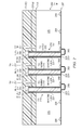
- FIG. 2 is a simplified cross-sectional depiction of a TSV die 200 comprising a plurality of TSVs 216 that include protruding TSV tips 217 having a protective layer 231 ( b ) over a first dielectric layer 231 ( a ) between and over the protruding TSV tips 217 on the bottomside 210 of the TSV die, according to an example embodiment.
- the protruding TSV tips 217 are shown having a metal cap 240 on the distal tip end 217 ( a ).
- TSV die 200 comprises a substrate 205 including a topside surface 207 including active circuitry 209 and a bottomside surface 210 .
- the active circuitry 209 on TSV die 200 is configured to provide an IC circuit function, such as a logic function, for example.
- the connection to active circuitry 209 is optional, since the TSV may simply provide a through-die connection through the substrate 205 without connecting to active circuitry 209 (e.g., to a device attached to bottomside 210 of TSV die 200 ).
- the TSVs 216 comprise an outer dielectric sleeve 221 and an inner metal core 220 , and a metal diffusion TSV barrier layer 222 between the outer dielectric sleeve 221 and the inner metal core 220 .
- the TSVs 216 extends from the topside surface 207 to protruding TSV tip 217 emerging from the bottomside surface 210 .
- the protective layer 231 ( b ) is shown as a planarizing layer over protruding TSV tips 217 .
- the TSV tip ends 217 ( a ) extend out about 5 ⁇ m from the bottomside surface 210
- the metal caps 240 add about 5 ⁇ m in height to the TSV tips 217
- the protective layer 231 ( b ) thickness is in the range from 10 to 15 ⁇ m with first dielectric layer 231 ( a ) being about 3 ⁇ m thick.
- the protective layer 231 ( b ) is about 3 to 8 ⁇ m above the metal caps 240 on the TSV tips 217 .
- FIG. 3 shows an example protected stacked die precursor 300 comprising the TSV die 200 shown in FIG. 2 bonded to a workpiece shown as substrate 330 , according to an example embodiment.
- the protected stacked die precursor 300 having TSV tips encapsulated enables shipping of such units with a reduced risk of damaging the TSV tips.
- TSV die 200 is bonded topside 207 down to pads 337 on substrate 330 that is shown as a package substrate (e.g., organic substrate).
- the package substrate can comprise a ceramic or an organic substrate, that may be thin (e.g., ⁇ 350 ⁇ m).
- the package substrate is generally provided as a substrate panel (or strip).
- the assembling can comprise TC bonding.
- the TSV die 200 is shown including pillars 325 that are capped with solder 326 .
- Underfill 328 is shown between the TSV die 200 and the package substrate 330 .
- the package substrate 330 is shown including a ball grid array (BGA) comprising a plurality of solder balls 331 .
- BGA ball grid array
- Protected stacked die precursor 300 shown in FIG. 3 can be used to form a stacked die device (e.g., system in package (SIP)) including TC bonding the stacked die precursor 300 to a workpiece.
- the protective layer 231 ( b ) on the bottomside 210 of the TSV die 200 is partially or completely removed to expose the TSV tips 217 for subsequent bonding.
- a top IC die can be assembled onto the exposed TSV tips 217 of the TSV die 200 .
- the top IC die comprises a memory die
- the TSV die 200 comprises a logic die.
- the top die comprises an IC die stack comprising a plurality of stacked IC die that are bonded to one another.
- the reduced warpage of the TSV die 200 following TC bonding provided by the protective layer described above can also reduce failures with top die assembly onto the protruding TSV tips due to loss of co-planarity. Overmolding can follow, and then singulation to form a plurality of stacked die devices.
- method can further comprise attaching a BGA of solder balls to the bottom of the workpiece before singulation.
- the active circuitry formed on the substrate having a semiconductor surface comprises circuit elements that may generally include transistors, diodes, capacitors, and resistors, as well as signal lines and other electrical conductors that interconnect the various circuit elements to provide an IC circuit function.
- IC circuit function refers to circuit functions from ICs, that for example may include an application specific integrated circuit (ASIC), a digital signal processor, a radio frequency chip, a memory, a microcontroller and a system-on-a-chip or a combination thereof.
- ASIC application specific integrated circuit
- Disclosed embodiments can be integrated into a variety of process flows to form a variety of devices and related products.
- the semiconductor substrates may include various elements therein and/or layers thereon.
- barrier layers can include barrier layers, other dielectric layers, device structures, active elements and passive elements, including source regions, drain regions, bit lines, bases, emitters, collectors, conductive lines, conductive vias, etc.
- disclosed embodiments can be used in a variety of semiconductor device fabrication processes including bipolar, CMOS, BiCMOS and MEMS processes.
Landscapes
- Internal Circuitry In Semiconductor Integrated Circuit Devices (AREA)
- Wire Bonding (AREA)
Priority Applications (6)
| Application Number | Priority Date | Filing Date | Title |
|---|---|---|---|
| US13/150,899 US8623763B2 (en) | 2011-06-01 | 2011-06-01 | Protective layer for protecting TSV tips during thermo-compressive bonding |
| EP12792149.2A EP2783393A4 (en) | 2011-06-01 | 2012-06-01 | PROTECTIVE LAYER FOR THE PROTECTION OF TSV TIPS DURING A HEAT COMPRESSION CONNECTION |
| CN201280037713.4A CN103718286A (zh) | 2011-06-01 | 2012-06-01 | 热压键合期间用于保护tsv末端的保护层 |
| JP2014513727A JP6038902B2 (ja) | 2011-06-01 | 2012-06-01 | 熱圧着ボンディングの間tsvティップを保護するための保護層 |
| PCT/US2012/040388 WO2012167027A2 (en) | 2011-06-01 | 2012-06-01 | Protective layer for protecting tsv tips during thermo-compressive bonding |
| US13/894,536 US8723330B2 (en) | 2011-06-01 | 2013-05-15 | Protective layer for protecting TSV tips during thermo-compressive bonding |
Applications Claiming Priority (1)
| Application Number | Priority Date | Filing Date | Title |
|---|---|---|---|
| US13/150,899 US8623763B2 (en) | 2011-06-01 | 2011-06-01 | Protective layer for protecting TSV tips during thermo-compressive bonding |
Related Child Applications (1)
| Application Number | Title | Priority Date | Filing Date |
|---|---|---|---|
| US13/894,536 Division US8723330B2 (en) | 2011-06-01 | 2013-05-15 | Protective layer for protecting TSV tips during thermo-compressive bonding |
Publications (2)
| Publication Number | Publication Date |
|---|---|
| US20120306085A1 US20120306085A1 (en) | 2012-12-06 |
| US8623763B2 true US8623763B2 (en) | 2014-01-07 |
Family
ID=47260364
Family Applications (2)
| Application Number | Title | Priority Date | Filing Date |
|---|---|---|---|
| US13/150,899 Active 2031-10-17 US8623763B2 (en) | 2011-06-01 | 2011-06-01 | Protective layer for protecting TSV tips during thermo-compressive bonding |
| US13/894,536 Active 2031-06-12 US8723330B2 (en) | 2011-06-01 | 2013-05-15 | Protective layer for protecting TSV tips during thermo-compressive bonding |
Family Applications After (1)
| Application Number | Title | Priority Date | Filing Date |
|---|---|---|---|
| US13/894,536 Active 2031-06-12 US8723330B2 (en) | 2011-06-01 | 2013-05-15 | Protective layer for protecting TSV tips during thermo-compressive bonding |
Country Status (5)
| Country | Link |
|---|---|
| US (2) | US8623763B2 (enExample) |
| EP (1) | EP2783393A4 (enExample) |
| JP (1) | JP6038902B2 (enExample) |
| CN (1) | CN103718286A (enExample) |
| WO (1) | WO2012167027A2 (enExample) |
Cited By (2)
| Publication number | Priority date | Publication date | Assignee | Title |
|---|---|---|---|---|
| US20120193808A1 (en) * | 2011-02-01 | 2012-08-02 | Maxim Integrated Products, Inc. | Bonded stacked wafers and methods of electroplating bonded stacked wafers |
| US9978694B2 (en) | 2016-09-05 | 2018-05-22 | Samsung Electronics Co., Ltd. | Semiconductor package and method of fabricating the same |
Families Citing this family (13)
| Publication number | Priority date | Publication date | Assignee | Title |
|---|---|---|---|---|
| KR101916225B1 (ko) * | 2012-04-09 | 2018-11-07 | 삼성전자 주식회사 | Tsv를 구비한 반도체 칩 및 그 반도체 칩 제조방법 |
| US8907494B2 (en) | 2013-03-14 | 2014-12-09 | International Business Machines Corporation | Electrical leakage reduction in stacked integrated circuits having through-silicon-via (TSV) structures |
| CN104810319A (zh) * | 2014-01-28 | 2015-07-29 | 中芯国际集成电路制造(上海)有限公司 | 晶圆键合的方法 |
| EP2908337B1 (en) * | 2014-02-12 | 2025-11-12 | ams AG | Semiconductor device with a thermally stable bump contact on a TSV and method of producing such a semiconductor device |
| EP3167485A4 (en) * | 2014-07-11 | 2018-03-07 | Intel Corporation | Scalable package architecture and associated techniques and configurations |
| JP2016039512A (ja) * | 2014-08-08 | 2016-03-22 | キヤノン株式会社 | 電極が貫通配線と繋がったデバイス、及びその製造方法 |
| CN104502903B (zh) * | 2014-11-28 | 2017-12-29 | 成都嘉纳海威科技有限责任公司 | 一种基于tsv转接板的多波束接收sip系统 |
| WO2016154526A1 (en) * | 2015-03-26 | 2016-09-29 | Board Of Regents, The University Of Texas System | Capped through-silicon-vias for 3d integrated circuits |
| US11469194B2 (en) * | 2018-08-08 | 2022-10-11 | Stmicroelectronics S.R.L. | Method of manufacturing a redistribution layer, redistribution layer and integrated circuit including the redistribution layer |
| US11152333B2 (en) * | 2018-10-19 | 2021-10-19 | Micron Technology, Inc. | Semiconductor device packages with enhanced heat management and related systems |
| US12456662B2 (en) | 2020-12-28 | 2025-10-28 | Adeia Semiconductor Bonding Technologies Inc. | Structures with through-substrate vias and methods for forming the same |
| WO2022147430A1 (en) | 2020-12-28 | 2022-07-07 | Invensas Bonding Technologies, Inc. | Structures with through-substrate vias and methods for forming the same |
| US20250218903A1 (en) * | 2023-12-28 | 2025-07-03 | Adeia Semiconductor Bonding Technologies Inc. | Via reveal processing and structures |
Citations (9)
| Publication number | Priority date | Publication date | Assignee | Title |
|---|---|---|---|---|
| US7365436B2 (en) | 2004-11-08 | 2008-04-29 | Shinko Electric Industries Co., Ltd. | Substrate having a penetrating via and wiring connected to the penetrating via and a method for manufacturing the same |
| US7407833B2 (en) * | 2004-04-27 | 2008-08-05 | Advanced Semiconductor Engineering, Inc. | Process for fabricating chip package structure |
| US20080280435A1 (en) | 2005-11-08 | 2008-11-13 | Koninklijke Philips Electronics N.V. | Producing a Covered Through Substrate Via Using a Temporary Cap Layer |
| US20090278244A1 (en) * | 2008-05-12 | 2009-11-12 | Texas Instruments Inc | Ic device having low resistance tsv comprising ground connection |
| US20100038800A1 (en) | 2008-08-18 | 2010-02-18 | Samsung Electronics Co., Ltd. | Through-silicon via structures including conductive protective layers and methods of forming the same |
| US20100171226A1 (en) | 2008-12-29 | 2010-07-08 | Texas Instruments, Inc. | Ic having tsv arrays with reduced tsv induced stress |
| US20100230759A1 (en) | 2009-03-13 | 2010-09-16 | Hsueh-An Yang | Silicon Chip Having Through Via and Method for Making the Same |
| US8298944B1 (en) * | 2011-06-01 | 2012-10-30 | Texas Instruments Incorporated | Warpage control for die with protruding TSV tips during thermo-compressive bonding |
| US8313982B2 (en) * | 2010-09-20 | 2012-11-20 | Texas Instruments Incorporated | Stacked die assemblies including TSV die |
Family Cites Families (17)
| Publication number | Priority date | Publication date | Assignee | Title |
|---|---|---|---|---|
| EP1189271A3 (en) * | 1996-07-12 | 2003-07-16 | Fujitsu Limited | Wiring boards and mounting of semiconductor devices thereon |
| JP4151164B2 (ja) * | 1999-03-19 | 2008-09-17 | 株式会社デンソー | 半導体装置の製造方法 |
| US6734532B2 (en) * | 2001-12-06 | 2004-05-11 | Texas Instruments Incorporated | Back side coating of semiconductor wafers |
| US6713366B2 (en) * | 2002-06-12 | 2004-03-30 | Intel Corporation | Method of thinning a wafer utilizing a laminated reinforcing layer over the device side |
| US6864165B1 (en) * | 2003-09-15 | 2005-03-08 | International Business Machines Corporation | Method of fabricating integrated electronic chip with an interconnect device |
| WO2005106937A1 (ja) * | 2004-04-28 | 2005-11-10 | Lintec Corporation | シート剥離装置及び剥離方法 |
| JP2007317822A (ja) * | 2006-05-25 | 2007-12-06 | Sony Corp | 基板処理方法及び半導体装置の製造方法 |
| KR20090075883A (ko) * | 2006-10-31 | 2009-07-09 | 어드밴스드 마이크로 디바이시즈, 인코포레이티드 | 알루미늄 단자 금속층이 없는 금속화층 스택 |
| KR100871382B1 (ko) * | 2007-06-26 | 2008-12-02 | 주식회사 하이닉스반도체 | 관통 실리콘 비아 스택 패키지 및 그의 제조 방법 |
| JP5159273B2 (ja) * | 2007-11-28 | 2013-03-06 | ルネサスエレクトロニクス株式会社 | 電子装置の製造方法 |
| US7759212B2 (en) * | 2007-12-26 | 2010-07-20 | Stats Chippac, Ltd. | System-in-package having integrated passive devices and method therefor |
| US8334170B2 (en) * | 2008-06-27 | 2012-12-18 | Taiwan Semiconductor Manufacturing Company, Ltd. | Method for stacking devices |
| US7687311B1 (en) * | 2008-11-13 | 2010-03-30 | Taiwan Semiconductor Manufacturing Company, Ltd. | Method for producing stackable dies |
| JP5563785B2 (ja) * | 2009-05-14 | 2014-07-30 | 新光電気工業株式会社 | 半導体パッケージ及びその製造方法 |
| US20100327465A1 (en) * | 2009-06-25 | 2010-12-30 | Advanced Semiconductor Engineering, Inc. | Package process and package structure |
| TWI429055B (zh) * | 2010-10-07 | 2014-03-01 | 日月光半導體製造股份有限公司 | 堆疊式封裝結構及其製造方法 |
| CN102054787B (zh) | 2010-10-21 | 2013-08-14 | 日月光半导体制造股份有限公司 | 堆栈式封装结构及其制造方法 |
-
2011
- 2011-06-01 US US13/150,899 patent/US8623763B2/en active Active
-
2012
- 2012-06-01 CN CN201280037713.4A patent/CN103718286A/zh active Pending
- 2012-06-01 WO PCT/US2012/040388 patent/WO2012167027A2/en not_active Ceased
- 2012-06-01 EP EP12792149.2A patent/EP2783393A4/en not_active Withdrawn
- 2012-06-01 JP JP2014513727A patent/JP6038902B2/ja active Active
-
2013
- 2013-05-15 US US13/894,536 patent/US8723330B2/en active Active
Patent Citations (9)
| Publication number | Priority date | Publication date | Assignee | Title |
|---|---|---|---|---|
| US7407833B2 (en) * | 2004-04-27 | 2008-08-05 | Advanced Semiconductor Engineering, Inc. | Process for fabricating chip package structure |
| US7365436B2 (en) | 2004-11-08 | 2008-04-29 | Shinko Electric Industries Co., Ltd. | Substrate having a penetrating via and wiring connected to the penetrating via and a method for manufacturing the same |
| US20080280435A1 (en) | 2005-11-08 | 2008-11-13 | Koninklijke Philips Electronics N.V. | Producing a Covered Through Substrate Via Using a Temporary Cap Layer |
| US20090278244A1 (en) * | 2008-05-12 | 2009-11-12 | Texas Instruments Inc | Ic device having low resistance tsv comprising ground connection |
| US20100038800A1 (en) | 2008-08-18 | 2010-02-18 | Samsung Electronics Co., Ltd. | Through-silicon via structures including conductive protective layers and methods of forming the same |
| US20100171226A1 (en) | 2008-12-29 | 2010-07-08 | Texas Instruments, Inc. | Ic having tsv arrays with reduced tsv induced stress |
| US20100230759A1 (en) | 2009-03-13 | 2010-09-16 | Hsueh-An Yang | Silicon Chip Having Through Via and Method for Making the Same |
| US8313982B2 (en) * | 2010-09-20 | 2012-11-20 | Texas Instruments Incorporated | Stacked die assemblies including TSV die |
| US8298944B1 (en) * | 2011-06-01 | 2012-10-30 | Texas Instruments Incorporated | Warpage control for die with protruding TSV tips during thermo-compressive bonding |
Cited By (4)
| Publication number | Priority date | Publication date | Assignee | Title |
|---|---|---|---|---|
| US20120193808A1 (en) * | 2011-02-01 | 2012-08-02 | Maxim Integrated Products, Inc. | Bonded stacked wafers and methods of electroplating bonded stacked wafers |
| US8970043B2 (en) * | 2011-02-01 | 2015-03-03 | Maxim Integrated Products, Inc. | Bonded stacked wafers and methods of electroplating bonded stacked wafers |
| US9331048B2 (en) | 2011-02-01 | 2016-05-03 | Maxim Integrated Products, Inc. | Bonded stacked wafers and methods of electroplating bonded stacked wafers |
| US9978694B2 (en) | 2016-09-05 | 2018-05-22 | Samsung Electronics Co., Ltd. | Semiconductor package and method of fabricating the same |
Also Published As
| Publication number | Publication date |
|---|---|
| WO2012167027A3 (en) | 2013-04-25 |
| JP6038902B2 (ja) | 2016-12-07 |
| EP2783393A4 (en) | 2016-03-23 |
| EP2783393A2 (en) | 2014-10-01 |
| JP2014517531A (ja) | 2014-07-17 |
| CN103718286A (zh) | 2014-04-09 |
| US8723330B2 (en) | 2014-05-13 |
| WO2012167027A2 (en) | 2012-12-06 |
| US20130249098A1 (en) | 2013-09-26 |
| US20120306085A1 (en) | 2012-12-06 |
Similar Documents
| Publication | Publication Date | Title |
|---|---|---|
| US8623763B2 (en) | Protective layer for protecting TSV tips during thermo-compressive bonding | |
| US8298944B1 (en) | Warpage control for die with protruding TSV tips during thermo-compressive bonding | |
| US8344493B2 (en) | Warpage control features on the bottomside of TSV die lateral to protruding bottomside tips | |
| US10854567B2 (en) | 3D packages and methods for forming the same | |
| US11830745B2 (en) | 3D packages and methods for forming the same | |
| US9570368B2 (en) | Method of manufacturing semiconductor package including forming a recessed region in a substrate | |
| US9698028B2 (en) | Semiconductor package and method of manufacturing the same | |
| US9754908B2 (en) | Wafer with liquid molding compound and post-passivation interconnect | |
| TWI397977B (zh) | 積體電路結構及其形成方法 | |
| KR101887262B1 (ko) | 칩 패키지를 위한 구조물 및 그 형성 방법 | |
| US20140154880A1 (en) | Post-Polymer Revealing of Through-Substrate Via Tips | |
| US20230343737A1 (en) | Semiconductor packages and methods of forming the same | |
| US20070246821A1 (en) | Utra-thin substrate package technology | |
| US9041215B2 (en) | Single mask package apparatus and method | |
| US20250022825A1 (en) | Seal ring structure and method of forming same |
Legal Events
| Date | Code | Title | Description |
|---|---|---|---|
| AS | Assignment |
Owner name: TEXAS INSTRUMENT INCORPORATED, TEXAS Free format text: ASSIGNMENT OF ASSIGNORS INTEREST;ASSIGNOR:WEST, JEFFREY ALAN;REEL/FRAME:026386/0873 Effective date: 20110531 |
|
| STCF | Information on status: patent grant |
Free format text: PATENTED CASE |
|
| FPAY | Fee payment |
Year of fee payment: 4 |
|
| MAFP | Maintenance fee payment |
Free format text: PAYMENT OF MAINTENANCE FEE, 8TH YEAR, LARGE ENTITY (ORIGINAL EVENT CODE: M1552); ENTITY STATUS OF PATENT OWNER: LARGE ENTITY Year of fee payment: 8 |
|
| MAFP | Maintenance fee payment |
Free format text: PAYMENT OF MAINTENANCE FEE, 12TH YEAR, LARGE ENTITY (ORIGINAL EVENT CODE: M1553); ENTITY STATUS OF PATENT OWNER: LARGE ENTITY Year of fee payment: 12 |