US8400233B2 - Circuit for impedance matching - Google Patents
Circuit for impedance matching Download PDFInfo
- Publication number
- US8400233B2 US8400233B2 US12/950,024 US95002410A US8400233B2 US 8400233 B2 US8400233 B2 US 8400233B2 US 95002410 A US95002410 A US 95002410A US 8400233 B2 US8400233 B2 US 8400233B2
- Authority
- US
- United States
- Prior art keywords
- impedance
- component
- circuit
- frequency band
- input
- Prior art date
- Legal status (The legal status is an assumption and is not a legal conclusion. Google has not performed a legal analysis and makes no representation as to the accuracy of the status listed.)
- Active
Links
- 238000010586 diagram Methods 0.000 description 8
- 230000001419 dependent effect Effects 0.000 description 3
- 239000004065 semiconductor Substances 0.000 description 2
- 230000009466 transformation Effects 0.000 description 2
- LKJPSUCKSLORMF-UHFFFAOYSA-N Monolinuron Chemical compound CON(C)C(=O)NC1=CC=C(Cl)C=C1 LKJPSUCKSLORMF-UHFFFAOYSA-N 0.000 description 1
- 230000004075 alteration Effects 0.000 description 1
- 239000003990 capacitor Substances 0.000 description 1
- 230000007423 decrease Effects 0.000 description 1
- 230000000694 effects Effects 0.000 description 1
- 230000003993 interaction Effects 0.000 description 1
- 238000004519 manufacturing process Methods 0.000 description 1
- 238000005457 optimization Methods 0.000 description 1
- 230000008054 signal transmission Effects 0.000 description 1
Images


Classifications
-
- H—ELECTRICITY
- H03—ELECTRONIC CIRCUITRY
- H03H—IMPEDANCE NETWORKS, e.g. RESONANT CIRCUITS; RESONATORS
- H03H7/00—Multiple-port networks comprising only passive electrical elements as network components
- H03H7/38—Impedance-matching networks
-
- H—ELECTRICITY
- H04—ELECTRIC COMMUNICATION TECHNIQUE
- H04B—TRANSMISSION
- H04B1/00—Details of transmission systems, not covered by a single one of groups H04B3/00 - H04B13/00; Details of transmission systems not characterised by the medium used for transmission
- H04B1/02—Transmitters
- H04B1/04—Circuits
- H04B1/0458—Arrangements for matching and coupling between power amplifier and antenna or between amplifying stages
-
- H—ELECTRICITY
- H03—ELECTRONIC CIRCUITRY
- H03H—IMPEDANCE NETWORKS, e.g. RESONANT CIRCUITS; RESONATORS
- H03H7/00—Multiple-port networks comprising only passive electrical elements as network components
- H03H7/38—Impedance-matching networks
- H03H2007/386—Multiple band impedance matching
Definitions
- the impedance of an antenna is dependent on the spatial surroundings thereof. This impedance is therefore subject to severe fluctuations, particularly in the case of mobile radios.
- the radiated real power of a mobile radio is heavily dependent on the extent to which the impedance of the antenna matches the impedances of further electric components connected thereto, such as a power amplifier.
- the impedance of electric components is also dependent on the frequency of a transmitted signal.
- a plurality of frequency bands is used for signal transmission.
- To attain a maximum radiated real power it is necessary to match the impedances in a plurality of frequency bands which are used.
- the present invention specifies a circuit that can be used to match the impedance of a generator as flexibly as possible to the impedance of a load.
- Embodiments of the invention specify a circuit for impedance matching.
- the circuit has an input, which can be connected to a generator, for example, and an output, which can be connected to a load, for example.
- a generator for example
- a load for example.
- this may correspond to a power amplifier as a generator and to an antenna as a load.
- the antenna can also be used as a generator and the load can correspond to the input of a receiver.
- the circuit has a plurality of components that can each be described by an effective impedance.
- each of the components may be made up of one or more electric units.
- the interaction of the impedances of the electric units results in an effective impedance for the component.
- Such a component is subsequently also called an impedance element.
- a main path between the input and the output of the circuit contains two impedance elements connected in series with one another.
- a third impedance element is connected thereto such that a T configuration is obtained.
- the circuit comprises a further impedance element which is connected in parallel with the main path of the circuit.
- This configuration allows a flexible layout for a circuit for impedance matching and optimization and, in particular, expansion of the usable frequency range.
- each of the impedance elements is chosen independently of the other impedance elements from the set of inductances, capacitances and lines or is made up of a plurality of such electric units.
- the impedance elements arranged in the main path are embodied as capacitances and the third and further impedance elements are embodied as inductances.
- At least one impedance element is adjustable.
- at least one of the capacitances can have the capacitance value adjusted.
- adjustability is intended to mean at least two different capacitance values between which it is possible to select and switch to and from during operation of the circuit.
- the adjustability covers a multiplicity of possible capacitance values.
- the capacitance values of both capacitances are variable steplessly in a particular adjustment range.
- Variable capacitances of this kind can be used to match the impedance of a load flexibly to the impedance of a generator. By way of example, it is thus possible to optimize the real power within the largest possible tuning range for the load impedances. In particular, it is possible for alteration of the impedance of the load or of the generator to involve attainment of tuning for the impedances without needing to connect or disconnect individual circuit elements. In this case, a particularly inexpensive and space-saving circuit for impedance matching may result.
- the tuning range for the circuit can be optimized by means of suitable selection of the capacitances and of the inductances. In particular, it is determined by the magnitude of the adjustment ranges for the capacitances and by the fineness of the stepping between the adjustable capacitance values.
- a variable capacitance may be in the form of a switched capacitor in which the capacitance values can be adjusted, for example, using binary stepping, between a maximum value and a minimum value.
- An example of a switched capacitance is a MEMS capacitance.
- a capacitance is used in which the capacitance value can be varied steplessly within an adjustment range. By way of example, this is possible in the case of a varactor based on semiconductors or ferroelectrics, which can be used in a circuit as a steplessly variable capacitance.
- the two capacitances of the main path have identical adjustment ranges.
- the use of identical units reduces the complexity of the circuit and the costs of production.
- the capacitances may have different adjustment ranges.
- the capacitances and the inductances are chosen such that the impedances can be matched within a plurality of frequency bands simultaneously. This is advantageous particularly in the case of mobile radios, in which a plurality of frequency bands are used.
- circuit arrangement which comprises a plurality of circuits for impedance matching.
- the circuit arrangement has at least two circuits for impedance matching which are connected in series with one another.
- the circuit arrangement comprises two circuits for impedance matching, for example, which are connected in series with one another.
- a first circuit is dimensioned such that it can be used for matching the impedance in the first frequency band.
- One suitable instance of circuit dimensioning involves the circuit prompting no significant change in the impedances for a second frequency band.
- This circuit is therefore a passage element for the second frequency band.
- a suitably dimensioned second circuit can be used to attain matching impedance in the second frequency band.
- This further circuit is designed such that it has no significant effect on the impedance matching in the first frequency band and is therefore a passage element for the first frequency band.
- the circuit arrangement has at least two circuits for impedance matching which are connected in parallel with one another.
- Such a circuit arrangement can likewise be used for the simultaneous matching of the impedance in two frequency ranges.
- the impedance elements of the first circuit are chosen such that it can be used for matching the impedance in a first frequency band but is a band rejection filter for the second frequency band.
- the input and output impedances of the circuit are chosen such that their real parts are very much larger than the real parts of the generator and load impedances.
- a second circuit connected in parallel therewith is dimensioned such that it is a band rejection filter for the first frequency band and can be used for impedance matching for the second frequency band.
- Such a circuit arrangement can therefore be used to attain simultaneous impedance matching within a plurality of frequency bands.
- FIG. 1 schematically shows the arrangement of a circuit for impedance matching between a generator and a load
- FIG. 2 shows a circuit for impedance matching with four impedance elements
- FIG. 3 shows a circuit for impedance matching with two capacitances and two inductances
- FIG. 4A uses a Smith diagram and a Cartesian coordinate system to show the optimum load impedances for a circuit for impedance matching as shown in FIG. 3 for a first frequency;
- FIG. 4B uses a Smith diagram and a Cartesian coordinate system to show the optimum load impedances for a circuit for impedance matching as shown in FIG. 3 for a second frequency;
- FIGS. 5A and 5B use a Smith diagram and a Cartesian coordinate system to show the optimum load impedances for a circuit comprising a T configuration for the frequencies shown in FIGS. 4A and 4B ;
- FIGS. 6A and 6B use a Smith diagram and a Cartesian coordinate system to show the optimum load impedances for a further circuit for impedance matching as shown in FIG. 3 for two frequencies;
- FIGS. 7A and 7B use a Smith diagram and a Cartesian coordinate system to show the optimum load impedances for a further circuit for impedance matching as shown in FIG. 3 for two frequencies;
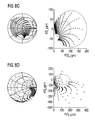
- FIGS. 8A to 8G show the optimum load impedances for a circuit for impedance matching as shown in FIG. 3 for various frequencies.
- FIG. 1 schematically shows a generator G which is connected to a load L via a circuit for impedance matching A.
- the circuit for impedance matching A is also called a matching network.
- the generator G corresponds to the output of a power amplifier and the load L corresponds to an antenna, for example.
- the generator G delivers an AC voltage u G and can be described by the complex generator impedance Z G .
- the load L is described by its complex load impedance Z L .
- the generator outputs a first real power P 1 to the matching network via the input IN.
- the matching network outputs a second real power P 2 to load L via the output OUT.
- the circuit for impedance matching is intended to be used to maximize the real power P 2 which is output to the load and hence to minimize the reflected power.
- the reflected power can be described by an input reflection factor R IN and an output reflection factor R OUT .
- On the generator side there is a whole circuit with the input impedance Z IN and a normalized input reflection factor R IN .
- the input reflection factor R IN is normalized to the generator impedance Z G .
- On the load side there is accordingly an output impedance Z OUT and a whole circuit with an output reflection factor R OUT .
- the output reflection factor R OUT is usually based on the output impedance Z OUT .
- reflectionless matching at the output of the matching network can be required.
- the load impedance Z L and hence the output impedance Z OUT are constant.
- FIG. 2 shows a circuit for impedance matching A, in which an input IN and an output OUT have two impedance elements Z 1 and Z 2 connected in series between them in a main path. These impedance elements form a T configuration together with a third impedance element Z 3 . A fourth impedance element Z 4 is connected in parallel with the main path between the input IN and the output OUT.
- the impedance elements Z 1 , Z 2 , Z 3 , Z 4 are capacitances, inductances or lines.
- Each impedance element may also be made up of a plurality of such elements which can be described by an effective total impedance.
- FIG. 3 shows a circuit for impedance matching A in which the impedance elements Z 1 , Z 2 connected in series in the main path are embodied as capacitances C 1 , C 2 .
- the third and further impedance elements are inductances L 1 and L 2 .
- the capacitances C 1 and C 2 are elements with adjustable capacitance values.
- the use of variable impedance elements allows the properties of the matching network A and particularly the tuning range thereof to be altered.
- Complex generator impedances are also possible.
- the output has a load with a load impedance Z L applied to it, for example.
- FIGS. 4A , 4 B, 6 A, 6 B, 7 A, 7 B and 8 A- 8 G have optimum load impedances Z L, OPT , at which reflectionless matching appears at the input, plotted for differently dimensioned matching networks as shown in FIG. 3 .
- FIGS. 5A and 5B have optimum load impedances Z L, OPT plotted which arise for a circuit which only comprises a T configuration without a further parallel impedance element.
- the optimum load impedances Z L, OPT are respectively plotted in a Smith diagram and in a Cartesian coordinate system. From the presentation of an optimum load impedance Z L, OPT in the Smith diagram, it is possible to ascertain the associated reflection factor and the standing wave ratio VSWR (Voltage Standing Wave Ratio).
- the optimum load impedances Z L, OPT are respectively normalized to a reference impedance of 50 ⁇ , which may correspond to the generator impedance Z G , for example.
- the imaginary part I(Z L, OPT ) of an optimum load impedance Z L, OPT is plotted against the real part R(Z L, OPT ) thereof.
- FIGS. 4A and 4B are based on a circuit for impedance matching as shown in FIG. 3 , wherein the capacitances C 1 and C 2 have an adjustment range of between 0.125 pF and 2 pF. The capacitance values have each been adjusted in sixteen steps in this range.
- the inductance L 1 has an inductance value of 4.9 nH and the inductance L 2 has an inductance value of 12.3 nH.
- Optimum load impedances Z L, OPT have been ascertained for two frequency bands of the mobile radio range. The calculations have respectively been based on the center frequency of the uplink range.
- optimum load impedances Z L, OPT have been ascertained for UMTS band I, in which the center frequency is 1950 MHz. In this case, a broad distribution for the optimum load impedances and hence a large matchable impedance range are obtained.
- optimum load impedances Z L, OPT have been ascertained for the GSM 900 frequency band, in which the center frequency is 897.5 MHz.
- the ratio of the center frequencies of the UMTS-band and of the GSM 900 band is 2.17.
- impedances around 50 ⁇ are easily matched in the GSM 900 band.
- the matching network can also be used as a passage element for this frequency band without impedance matching.
- FIGS. 5A and 5B have the optimum load impedances Z L, OPT plotted which are obtained for a circuit with a T configuration, i.e., without the inductance L 2 .
- the capacitances C 1 and C 2 are designed like the capacitances shown in FIGS. 4A and 4B and are varied in the same range.
- the inductance L 1 has an inductance value of 7.35 nH.
- FIG. 5B has the optimum load impedances plotted for the center frequency of the GMS 900 band.
- generator impedances around 50 ⁇ can no longer be matched in reflectionless fashion. Therefore, this matching network cannot be used as a passage element in this frequency range.
- FIGS. 6A and 6B have optimum load impedances plotted for the frequency bands GSM 900 and GSM 1800.
- the capacitances C 1 and C 2 and the inductances L 1 and L 2 are chosen such that the largest possible tuning range is obtained in both frequency bands.
- the capacitances C 1 and C 2 have been adjusted in sixteen steps between 0.125 pF and 2 pF.
- the inductance L 1 has an inductance value of 5.5 nH and the inductance L 2 has an inductance value of 10.9 nH.
- the center frequency in the uplink range is 1747.5 MHz for the GSM 1800 band and 897.5 MHz for the GSM 900 band. This gives a ratio for the center frequencies of 1.95.
- FIG. 6A has the optimum load impedances Z L, OPT plotted for the GSM 1800 band. As can be seen from the presentation in the Cartesian coordinate system, a large matchable impedance range is obtained.
- FIG. 6B has the optimum load impedances Z L, OPT plotted for the center frequency of the GSM 900 band. With this circuit dimensioning, generator impedances around 50 ⁇ are easily matched. Alternatively, this matching network can be used as a passage element in the 897.5 MHZ range without impedance transformation.
- FIGS. 7A and 7B have optimum load impedances Z L, OPT plotted for the frequency bands GSM 900 and GSM 1800.
- the basis is a circuit for impedance matching as shown in FIG. 3 , wherein the capacitances C 1 and C 2 have different adjustment ranges.
- the capacitance C 1 can be adjusted in the range from 0.176 pF to 2.82 pF and the capacitance C 2 can be adjusted in the range from 0.125 pF to 2 pF. Both capacitances can be varied in sixteen steps.
- the inductance L 1 has a value of 6.8 nH and the inductance L 2 has a value of 13.7 nH.
- FIGS. 8A to 8G show the broadband properties of this matching network.
- FIG. 8A has optimum load impedances plotted for a frequency of 824 MHz. This corresponds to the lower frequency limit of the GSM 850 uplink band and to the lowest operating frequency of UMTS bands I to X.
- FIG. 8B has optimum load impedances plotted for a frequency of 880 MHz. This frequency is the lower frequency limit of the GSM 900 uplink band.
- FIG. 8C has optimum load impedances plotted for a frequency of 960 MHz. This corresponds to the upper frequency limit of the GSM 900 downlink band.
- the matching network can be used in the whole frequency range from 824 to 960 MHz for impedance transformation to a generator impedance of 50 ⁇ .
- this matching network can also be used as a passage element in this case. If the generator impedances differ from 50 ⁇ , an optimum tuning range can be attained by virtue of another choice of capacitances C 1 and C 2 and of inductances L 1 and L 2 .
- FIG. 8D has optimum load impedances plotted for a frequency of 1710 MHz. This corresponds to a lower frequency limit of the GSM 1800 uplink band.
- FIG. 8E has optimum load impedances plotted for a frequency of 1880 MHz. This corresponds to the upper frequency limit of the GSM 1800 downlink band and is at the same time the center frequency of the GSM 1900 uplink band.
- FIG. 8F has optimum load impedances plotted for a frequency of 1980 MHz. This corresponds to the upper frequency limit of the UMTS I uplink band and is 10 MHz below the upper frequency limit of the GSM 1900 downlink band.
- FIG. 8G has optimum load impedances plotted for a frequency of 2170 MHz. This corresponds to the upper frequency limit of the UMTS I downlink band and is at the same time the highest operating frequency of UMTS bands Ito VI and VIII to X.
- variable capacitances are used which can be altered continuously in an adjustment range.
- these are ferroelectric varactors or semiconductor varactors.
- the invention is not limited to the exemplary embodiments by virtue of the description thereof but rather comprises any new feature and any combination of features. This includes particularly any combination of features in the patent claims, even if this feature or this combination is itself not explicitly specified in the patent claims or exemplary embodiments.
Landscapes
- Engineering & Computer Science (AREA)
- Computer Networks & Wireless Communication (AREA)
- Signal Processing (AREA)
- Transmitters (AREA)
- Amplifiers (AREA)
- Networks Using Active Elements (AREA)
Priority Applications (1)
| Application Number | Priority Date | Filing Date | Title |
|---|---|---|---|
| US13/609,923 US20130005288A1 (en) | 2008-05-21 | 2012-09-11 | Circuit for Impedance Matching |
Applications Claiming Priority (4)
| Application Number | Priority Date | Filing Date | Title |
|---|---|---|---|
| DE102008024482.1A DE102008024482B4 (de) | 2008-05-21 | 2008-05-21 | Schaltungsanordnung zur Impedanzanpassung, elektronisches Bauelement und Mobilfunkgerät |
| DE102008024482.1 | 2008-05-21 | ||
| DE102008024482 | 2008-05-21 | ||
| PCT/EP2009/056092 WO2009141358A1 (de) | 2008-05-21 | 2009-05-19 | Schaltung zur impedanzanpassung |
Related Parent Applications (1)
| Application Number | Title | Priority Date | Filing Date |
|---|---|---|---|
| PCT/EP2009/056092 Continuation WO2009141358A1 (de) | 2008-05-21 | 2009-05-19 | Schaltung zur impedanzanpassung |
Related Child Applications (1)
| Application Number | Title | Priority Date | Filing Date |
|---|---|---|---|
| US13/609,923 Continuation US20130005288A1 (en) | 2008-05-21 | 2012-09-11 | Circuit for Impedance Matching |
Publications (2)
| Publication Number | Publication Date |
|---|---|
| US20110090021A1 US20110090021A1 (en) | 2011-04-21 |
| US8400233B2 true US8400233B2 (en) | 2013-03-19 |
Family
ID=41131671
Family Applications (2)
| Application Number | Title | Priority Date | Filing Date |
|---|---|---|---|
| US12/950,024 Active US8400233B2 (en) | 2008-05-21 | 2010-11-19 | Circuit for impedance matching |
| US13/609,923 Abandoned US20130005288A1 (en) | 2008-05-21 | 2012-09-11 | Circuit for Impedance Matching |
Family Applications After (1)
| Application Number | Title | Priority Date | Filing Date |
|---|---|---|---|
| US13/609,923 Abandoned US20130005288A1 (en) | 2008-05-21 | 2012-09-11 | Circuit for Impedance Matching |
Country Status (4)
| Country | Link |
|---|---|
| US (2) | US8400233B2 (ja) |
| JP (2) | JP2011521577A (ja) |
| DE (1) | DE102008024482B4 (ja) |
| WO (1) | WO2009141358A1 (ja) |
Families Citing this family (4)
| Publication number | Priority date | Publication date | Assignee | Title |
|---|---|---|---|---|
| DE102010008920A1 (de) * | 2010-02-23 | 2011-08-25 | Epcos Ag, 81669 | Breitbandig betreibbare Impedanzanpassschaltung |
| KR101778117B1 (ko) * | 2011-03-22 | 2017-09-27 | 숭실대학교산학협력단 | 메타 전자파 구조를 이용한 이중대역 Class- F GaN 전력증폭장치 |
| US9325355B2 (en) * | 2013-02-14 | 2016-04-26 | Blackberry Limited | Methods and apparatus for performing impedance matching |
| US10700666B2 (en) | 2017-02-08 | 2020-06-30 | Taiyo Yuden Co., Ltd. | Filter circuit, multiplexer, and module |
Citations (15)
| Publication number | Priority date | Publication date | Assignee | Title |
|---|---|---|---|---|
| US3116373A (en) * | 1962-09-07 | 1963-12-31 | Gen Electric | Bridged-t time delay network |
| US3474181A (en) | 1966-06-02 | 1969-10-21 | Hammond Corp | Electrical musical instrument animator of the scanned progressive phase shift type |
| US4443772A (en) * | 1981-12-10 | 1984-04-17 | Rca Corporation | Switching microwave integrated bridge T group delay equalizer |
| US4763087A (en) | 1986-05-27 | 1988-08-09 | Schrader Paul D | Impedance matching network |
| US5202651A (en) * | 1990-12-27 | 1993-04-13 | Sharp Kabushiki Kaisha | Band-stop filter circuit suitably made into monolithic microwave integrated circuits |
| US6531933B2 (en) * | 2001-03-23 | 2003-03-11 | Sanyo Electric Co., Ltd. | Filter unit having two attenuation poles |
| EP0685936B1 (en) | 1994-05-25 | 2003-09-24 | Nokia Corporation | Adaptive antenna matching |
| US6765540B2 (en) | 2001-04-11 | 2004-07-20 | Kyocera Wireless Corp. | Tunable antenna matching circuit |
| US6895225B1 (en) | 1999-03-29 | 2005-05-17 | Nokia Mobile Phones, Ltd. | System for matching an antenna for a wireless communication device |
| US7012483B2 (en) | 2003-04-21 | 2006-03-14 | Agile Materials And Technologies, Inc. | Tunable bridge circuit |
| US20060160501A1 (en) | 2000-07-20 | 2006-07-20 | Greg Mendolia | Tunable microwave devices with auto-adjusting matching circuit |
| WO2006083432A1 (en) | 2005-01-28 | 2006-08-10 | Northrop Grumman Corporation | Monolithically integrated switchable circuits with mems |
| US7176845B2 (en) | 2002-02-12 | 2007-02-13 | Kyocera Wireless Corp. | System and method for impedance matching an antenna to sub-bands in a communication band |
| US7202747B2 (en) | 2003-08-05 | 2007-04-10 | Agile Materials And Technologies, Inc. | Self-tuning variable impedance circuit for impedance matching of power amplifiers |
| WO2007103537A2 (en) | 2006-03-08 | 2007-09-13 | Wispry, Inc. | Tunable impedance matching networks and tunable diplexer matching systems |
Family Cites Families (17)
| Publication number | Priority date | Publication date | Assignee | Title |
|---|---|---|---|---|
| JPS63183727U (ja) * | 1987-05-19 | 1988-11-25 | ||
| JP2602039B2 (ja) * | 1987-12-09 | 1997-04-23 | セイコーエプソン株式会社 | アンテナ回路及びテレビジョン受信機 |
| JPH0344207A (ja) * | 1989-07-12 | 1991-02-26 | Fujitsu Ltd | 広帯域光受信器のt字型整合回路 |
| JPH04298122A (ja) * | 1991-03-26 | 1992-10-21 | Sumitomo Chem Co Ltd | 自動車用アンテナ装置 |
| JPH0536930U (ja) * | 1991-10-18 | 1993-05-18 | アルプス電気株式会社 | 平衡型発振器の共振回路 |
| JP2826433B2 (ja) * | 1993-02-26 | 1998-11-18 | 日本電気株式会社 | アンテナ用二周波整合回路 |
| JP2914104B2 (ja) * | 1993-06-30 | 1999-06-28 | 三菱電機株式会社 | 放電加工方法及びその装置、並びにこの放電加工装置に適用可能な、静電容量可変装置及びインダクタンス可変装置 |
| JP3336868B2 (ja) * | 1996-08-09 | 2002-10-21 | 株式会社村田製作所 | 周波数の異なる複数の信号に整合する高周波増幅器 |
| JP3436850B2 (ja) * | 1996-08-09 | 2003-08-18 | 株式会社村田製作所 | 周波数の異なる複数の信号に整合する無線通信機用の高周波増幅器 |
| US5999134A (en) * | 1996-12-19 | 1999-12-07 | Ppg Industries Ohio, Inc. | Glass antenna system with an impedance matching network |
| US5969582A (en) * | 1997-07-03 | 1999-10-19 | Ericsson Inc. | Impedance matching circuit for power amplifier |
| JP3883707B2 (ja) * | 1998-08-28 | 2007-02-21 | 三菱電機株式会社 | 2周波整合回路 |
| JP2001185962A (ja) * | 1999-12-27 | 2001-07-06 | Toshiba Corp | 増幅器 |
| JP4216124B2 (ja) * | 2002-12-12 | 2009-01-28 | 三菱電機株式会社 | 2周波整合回路 |
| JP4821224B2 (ja) * | 2005-09-08 | 2011-11-24 | 株式会社ケンウッド | アンテナ整合装置及びアンテナ整合方法 |
| CN101558560A (zh) * | 2007-04-09 | 2009-10-14 | 松下电器产业株式会社 | 双频匹配电路 |
| JP4308889B2 (ja) * | 2007-08-29 | 2009-08-05 | パナソニック株式会社 | 2周波整合回路及びそれを具備する携帯端末 |
-
2008
- 2008-05-21 DE DE102008024482.1A patent/DE102008024482B4/de active Active
-
2009
- 2009-05-19 WO PCT/EP2009/056092 patent/WO2009141358A1/de active Application Filing
- 2009-05-19 JP JP2011509968A patent/JP2011521577A/ja not_active Withdrawn
-
2010
- 2010-11-19 US US12/950,024 patent/US8400233B2/en active Active
-
2012
- 2012-09-11 US US13/609,923 patent/US20130005288A1/en not_active Abandoned
-
2014
- 2014-07-18 JP JP2014148274A patent/JP5908539B2/ja active Active
Patent Citations (17)
| Publication number | Priority date | Publication date | Assignee | Title |
|---|---|---|---|---|
| US3116373A (en) * | 1962-09-07 | 1963-12-31 | Gen Electric | Bridged-t time delay network |
| US3474181A (en) | 1966-06-02 | 1969-10-21 | Hammond Corp | Electrical musical instrument animator of the scanned progressive phase shift type |
| US4443772A (en) * | 1981-12-10 | 1984-04-17 | Rca Corporation | Switching microwave integrated bridge T group delay equalizer |
| US4763087A (en) | 1986-05-27 | 1988-08-09 | Schrader Paul D | Impedance matching network |
| US5202651A (en) * | 1990-12-27 | 1993-04-13 | Sharp Kabushiki Kaisha | Band-stop filter circuit suitably made into monolithic microwave integrated circuits |
| EP0685936B1 (en) | 1994-05-25 | 2003-09-24 | Nokia Corporation | Adaptive antenna matching |
| US6895225B1 (en) | 1999-03-29 | 2005-05-17 | Nokia Mobile Phones, Ltd. | System for matching an antenna for a wireless communication device |
| US20060160501A1 (en) | 2000-07-20 | 2006-07-20 | Greg Mendolia | Tunable microwave devices with auto-adjusting matching circuit |
| US6531933B2 (en) * | 2001-03-23 | 2003-03-11 | Sanyo Electric Co., Ltd. | Filter unit having two attenuation poles |
| US6765540B2 (en) | 2001-04-11 | 2004-07-20 | Kyocera Wireless Corp. | Tunable antenna matching circuit |
| US7009455B2 (en) | 2001-04-11 | 2006-03-07 | Kyocera Wireless Corp. | Tunable power amplifier matching circuit |
| US7221327B2 (en) | 2001-04-11 | 2007-05-22 | Kyocera Wireless Corp. | Tunable matching circuit |
| US7176845B2 (en) | 2002-02-12 | 2007-02-13 | Kyocera Wireless Corp. | System and method for impedance matching an antenna to sub-bands in a communication band |
| US7012483B2 (en) | 2003-04-21 | 2006-03-14 | Agile Materials And Technologies, Inc. | Tunable bridge circuit |
| US7202747B2 (en) | 2003-08-05 | 2007-04-10 | Agile Materials And Technologies, Inc. | Self-tuning variable impedance circuit for impedance matching of power amplifiers |
| WO2006083432A1 (en) | 2005-01-28 | 2006-08-10 | Northrop Grumman Corporation | Monolithically integrated switchable circuits with mems |
| WO2007103537A2 (en) | 2006-03-08 | 2007-09-13 | Wispry, Inc. | Tunable impedance matching networks and tunable diplexer matching systems |
Non-Patent Citations (3)
| Title |
|---|
| Arell, T., et al., "A Unique 2 to 6 GHz 1 Watt High Efficiency GaAs MMIC Amplifierdesign Using All-Pass Matching Networks," Gallium Arsenide Integrated Circuit Symposium, 14th Annual IEEE, Oct. 4-7, 1992, 5 pages, Miami Beach, FL. |
| Kurokawa, K. "Power Waves and the Scattering Matrix," IEEE Transactions on Microwave Theory and Techniques, Mar. 1965, pp. 194-202. |
| Scheele, P, et al., "Continuously Tunable Impedance Matching Network Using Ferroelectric Varactors," 2005 IEEE MTT-S International, Microwave Symposium Digest, Jun. 12-17, 2005, 5 pages. |
Also Published As
| Publication number | Publication date |
|---|---|
| JP5908539B2 (ja) | 2016-04-26 |
| JP2014239486A (ja) | 2014-12-18 |
| US20130005288A1 (en) | 2013-01-03 |
| DE102008024482A1 (de) | 2009-11-26 |
| DE102008024482B4 (de) | 2016-10-06 |
| WO2009141358A1 (de) | 2009-11-26 |
| JP2011521577A (ja) | 2011-07-21 |
| US20110090021A1 (en) | 2011-04-21 |
Similar Documents
| Publication | Publication Date | Title |
|---|---|---|
| US7633355B2 (en) | Variable matching circuit | |
| US10424841B2 (en) | Antenna matching circuit, antenna circuit, front-end circuit, and communication apparatus | |
| US10062629B2 (en) | Antenna impedance matching and aperture tuning circuitry | |
| US10193521B2 (en) | Adjustable impedance matching network | |
| US8395459B2 (en) | Methods for tuning an adaptive impedance matching network with a look-up table | |
| US9647631B2 (en) | Tunable impedance matching network | |
| TWI426746B (zh) | 射頻處理裝置、射頻處理方法及相關無線通訊裝置 | |
| CN1511357A (zh) | 可调双频天线系统 | |
| JP2016048937A (ja) | 平面アンテナ用のインピーダンス整合回路 | |
| EP1738472A2 (en) | Apparatus, methods and articles of manufacture for output impedance matching using multi-band signal processing | |
| US9680441B2 (en) | Impedance matching circuit and antenna system | |
| US8400233B2 (en) | Circuit for impedance matching | |
| US20230198558A1 (en) | Impedance tuning circuits, devices and methods | |
| JP5488962B2 (ja) | アンテナ回路 | |
| US20210376465A1 (en) | Method and apparatus for implementing reflection type phase shifters (rtps) in a communication system | |
| US7129907B2 (en) | Broadband tunable antenna and transceiver systems | |
| TW201445899A (zh) | 射頻匹配電路及無線通訊裝置 | |
| US9455686B1 (en) | Wireless communication device and tunable filter thereof | |
| RU2649050C1 (ru) | Микроволновый аналоговый фазовращатель и система, содержащая его | |
| US20220311461A1 (en) | Agile harmonic filtering | |
| US7683737B2 (en) | Broadband phase shifter | |
| KR101473717B1 (ko) | 광대역 모듈 및 이를 포함하는 통신 장치 | |
| JP2004532565A (ja) | 送信器の効率を向上させるための方法及び装置 | |
| US20220166447A1 (en) | Out-of-band noise optimization for dual-band front-end modules | |
| JPH10163916A (ja) | 携帯無線端末機用アンテナ |
Legal Events
| Date | Code | Title | Description |
|---|---|---|---|
| AS | Assignment |
Owner name: EPCOS AG, GERMANY Free format text: ASSIGNMENT OF ASSIGNORS INTEREST;ASSIGNORS:SCHEELE, PATRICK;SCHMIDT, MATTHIAS;SIGNING DATES FROM 20101217 TO 20101222;REEL/FRAME:025591/0940 |
|
| STCF | Information on status: patent grant |
Free format text: PATENTED CASE |
|
| AS | Assignment |
Owner name: QUALCOMM TECHNOLOGIES, INC., CALIFORNIA Free format text: ASSIGNMENT OF ASSIGNORS INTEREST;ASSIGNOR:EPCOS AG;REEL/FRAME:031590/0576 Effective date: 20131111 |
|
| FPAY | Fee payment |
Year of fee payment: 4 |
|
| MAFP | Maintenance fee payment |
Free format text: PAYMENT OF MAINTENANCE FEE, 8TH YEAR, LARGE ENTITY (ORIGINAL EVENT CODE: M1552); ENTITY STATUS OF PATENT OWNER: LARGE ENTITY Year of fee payment: 8 |