US8089615B2 - Substrate holding apparatus, exposure apparatus, exposing method, and device fabricating method - Google Patents
Substrate holding apparatus, exposure apparatus, exposing method, and device fabricating method Download PDFInfo
- Publication number
- US8089615B2 US8089615B2 US12/155,514 US15551408A US8089615B2 US 8089615 B2 US8089615 B2 US 8089615B2 US 15551408 A US15551408 A US 15551408A US 8089615 B2 US8089615 B2 US 8089615B2
- Authority
- US
- United States
- Prior art keywords
- circumferential wall
- substrate
- space
- holding apparatus
- substrate holding
- Prior art date
- Legal status (The legal status is an assumption and is not a legal conclusion. Google has not performed a legal analysis and makes no representation as to the accuracy of the status listed.)
- Expired - Fee Related, expires
Links
- 239000000758 substrate Substances 0.000 title claims abstract description 338
- 238000000034 method Methods 0.000 title claims description 36
- 239000012530 fluid Substances 0.000 claims abstract description 63
- 239000007788 liquid Substances 0.000 claims description 146
- 238000007654 immersion Methods 0.000 claims description 29
- 230000003287 optical effect Effects 0.000 description 61
- 239000000463 material Substances 0.000 description 52
- 238000011084 recovery Methods 0.000 description 20
- 230000008569 process Effects 0.000 description 12
- XLYOFNOQVPJJNP-UHFFFAOYSA-N water Substances O XLYOFNOQVPJJNP-UHFFFAOYSA-N 0.000 description 8
- 238000005259 measurement Methods 0.000 description 7
- 238000010586 diagram Methods 0.000 description 6
- 239000010408 film Substances 0.000 description 6
- PEDCQBHIVMGVHV-UHFFFAOYSA-N Glycerine Chemical compound OCC(O)CO PEDCQBHIVMGVHV-UHFFFAOYSA-N 0.000 description 5
- 238000001514 detection method Methods 0.000 description 5
- 238000005286 illumination Methods 0.000 description 5
- 230000002940 repellent Effects 0.000 description 5
- 239000005871 repellent Substances 0.000 description 5
- 239000004065 semiconductor Substances 0.000 description 5
- VYPSYNLAJGMNEJ-UHFFFAOYSA-N Silicium dioxide Chemical compound O=[Si]=O VYPSYNLAJGMNEJ-UHFFFAOYSA-N 0.000 description 4
- 230000009467 reduction Effects 0.000 description 4
- YCKRFDGAMUMZLT-UHFFFAOYSA-N Fluorine atom Chemical compound [F] YCKRFDGAMUMZLT-UHFFFAOYSA-N 0.000 description 3
- WUKWITHWXAAZEY-UHFFFAOYSA-L calcium difluoride Chemical compound [F-].[F-].[Ca+2] WUKWITHWXAAZEY-UHFFFAOYSA-L 0.000 description 3
- 229910052731 fluorine Inorganic materials 0.000 description 3
- 239000011737 fluorine Substances 0.000 description 3
- 230000007246 mechanism Effects 0.000 description 3
- VLKZOEOYAKHREP-UHFFFAOYSA-N n-Hexane Chemical compound CCCCCC VLKZOEOYAKHREP-UHFFFAOYSA-N 0.000 description 3
- 230000037361 pathway Effects 0.000 description 3
- KFZMGEQAYNKOFK-UHFFFAOYSA-N Isopropanol Chemical compound CC(C)O KFZMGEQAYNKOFK-UHFFFAOYSA-N 0.000 description 2
- IMNFDUFMRHMDMM-UHFFFAOYSA-N N-Heptane Chemical compound CCCCCCC IMNFDUFMRHMDMM-UHFFFAOYSA-N 0.000 description 2
- WCUXLLCKKVVCTQ-UHFFFAOYSA-M Potassium chloride Chemical compound [Cl-].[K+] WCUXLLCKKVVCTQ-UHFFFAOYSA-M 0.000 description 2
- NNBZCPXTIHJBJL-UHFFFAOYSA-N decalin Chemical compound C1CCCC2CCCCC21 NNBZCPXTIHJBJL-UHFFFAOYSA-N 0.000 description 2
- DIOQZVSQGTUSAI-UHFFFAOYSA-N decane Chemical compound CCCCCCCCCC DIOQZVSQGTUSAI-UHFFFAOYSA-N 0.000 description 2
- 210000003608 fece Anatomy 0.000 description 2
- 239000010436 fluorite Substances 0.000 description 2
- YBMRDBCBODYGJE-UHFFFAOYSA-N germanium dioxide Chemical compound O=[Ge]=O YBMRDBCBODYGJE-UHFFFAOYSA-N 0.000 description 2
- 235000011187 glycerol Nutrition 0.000 description 2
- PQXKHYXIUOZZFA-UHFFFAOYSA-M lithium fluoride Chemical compound [Li+].[F-] PQXKHYXIUOZZFA-UHFFFAOYSA-M 0.000 description 2
- 229920002120 photoresistant polymer Polymers 0.000 description 2
- -1 polytetrafluoroethylene Polymers 0.000 description 2
- 230000001681 protective effect Effects 0.000 description 2
- 239000010453 quartz Substances 0.000 description 2
- PUZPDOWCWNUUKD-UHFFFAOYSA-M sodium fluoride Chemical compound [F-].[Na+] PUZPDOWCWNUUKD-UHFFFAOYSA-M 0.000 description 2
- 239000010409 thin film Substances 0.000 description 2
- 238000013519 translation Methods 0.000 description 2
- 239000004925 Acrylic resin Substances 0.000 description 1
- 229920000178 Acrylic resin Polymers 0.000 description 1
- 238000000018 DNA microarray Methods 0.000 description 1
- 240000007594 Oryza sativa Species 0.000 description 1
- 235000007164 Oryza sativa Nutrition 0.000 description 1
- 239000004721 Polyphenylene oxide Substances 0.000 description 1
- XUIMIQQOPSSXEZ-UHFFFAOYSA-N Silicon Chemical compound [Si] XUIMIQQOPSSXEZ-UHFFFAOYSA-N 0.000 description 1
- 239000002253 acid Substances 0.000 description 1
- OYLGJCQECKOTOL-UHFFFAOYSA-L barium fluoride Chemical compound [F-].[F-].[Ba+2] OYLGJCQECKOTOL-UHFFFAOYSA-L 0.000 description 1
- 229910001632 barium fluoride Inorganic materials 0.000 description 1
- 229910001634 calcium fluoride Inorganic materials 0.000 description 1
- 238000001444 catalytic combustion detection Methods 0.000 description 1
- 239000010627 cedar oil Substances 0.000 description 1
- 239000000919 ceramic Substances 0.000 description 1
- 230000003749 cleanliness Effects 0.000 description 1
- 239000000470 constituent Substances 0.000 description 1
- WVIIMZNLDWSIRH-UHFFFAOYSA-N cyclohexylcyclohexane Chemical group C1CCCCC1C1CCCCC1 WVIIMZNLDWSIRH-UHFFFAOYSA-N 0.000 description 1
- 230000006866 deterioration Effects 0.000 description 1
- 239000010419 fine particle Substances 0.000 description 1
- 150000002222 fluorine compounds Chemical class 0.000 description 1
- 230000004907 flux Effects 0.000 description 1
- 239000002223 garnet Substances 0.000 description 1
- 229940119177 germanium dioxide Drugs 0.000 description 1
- 239000011521 glass Substances 0.000 description 1
- 230000031700 light absorption Effects 0.000 description 1
- 239000004973 liquid crystal related substance Substances 0.000 description 1
- 238000004519 manufacturing process Methods 0.000 description 1
- QSHDDOUJBYECFT-UHFFFAOYSA-N mercury Chemical compound [Hg] QSHDDOUJBYECFT-UHFFFAOYSA-N 0.000 description 1
- 229910052753 mercury Inorganic materials 0.000 description 1
- 229910052751 metal Inorganic materials 0.000 description 1
- 239000002184 metal Substances 0.000 description 1
- 239000003921 oil Substances 0.000 description 1
- 239000003960 organic solvent Substances 0.000 description 1
- TWNQGVIAIRXVLR-UHFFFAOYSA-N oxo(oxoalumanyloxy)alumane Chemical compound O=[Al]O[Al]=O TWNQGVIAIRXVLR-UHFFFAOYSA-N 0.000 description 1
- 238000012858 packaging process Methods 0.000 description 1
- 238000000206 photolithography Methods 0.000 description 1
- 238000005498 polishing Methods 0.000 description 1
- 229920000570 polyether Polymers 0.000 description 1
- 229920001343 polytetrafluoroethylene Polymers 0.000 description 1
- 239000004810 polytetrafluoroethylene Substances 0.000 description 1
- 239000001103 potassium chloride Substances 0.000 description 1
- 235000011164 potassium chloride Nutrition 0.000 description 1
- 235000009566 rice Nutrition 0.000 description 1
- 235000002020 sage Nutrition 0.000 description 1
- 229910052594 sapphire Inorganic materials 0.000 description 1
- 239000010980 sapphire Substances 0.000 description 1
- 238000005389 semiconductor device fabrication Methods 0.000 description 1
- 229910052710 silicon Inorganic materials 0.000 description 1
- 239000010703 silicon Substances 0.000 description 1
- 239000000377 silicon dioxide Substances 0.000 description 1
- 235000013024 sodium fluoride Nutrition 0.000 description 1
- 239000011775 sodium fluoride Substances 0.000 description 1
- 235000013599 spices Nutrition 0.000 description 1
- FVRNDBHWWSPNOM-UHFFFAOYSA-L strontium fluoride Chemical compound [F-].[F-].[Sr+2] FVRNDBHWWSPNOM-UHFFFAOYSA-L 0.000 description 1
- 229910001637 strontium fluoride Inorganic materials 0.000 description 1
- 239000000126 substance Substances 0.000 description 1
- 238000002834 transmittance Methods 0.000 description 1
- 238000009834 vaporization Methods 0.000 description 1
- 230000008016 vaporization Effects 0.000 description 1
- PXXNTAGJWPJAGM-UHFFFAOYSA-N vertaline Natural products C1C2C=3C=C(OC)C(OC)=CC=3OC(C=C3)=CC=C3CCC(=O)OC1CC1N2CCCC1 PXXNTAGJWPJAGM-UHFFFAOYSA-N 0.000 description 1
- 230000003313 weakening effect Effects 0.000 description 1
Images


Classifications
-
- H—ELECTRICITY
- H01—ELECTRIC ELEMENTS
- H01L—SEMICONDUCTOR DEVICES NOT COVERED BY CLASS H10
- H01L21/00—Processes or apparatus adapted for the manufacture or treatment of semiconductor or solid state devices or of parts thereof
- H01L21/67—Apparatus specially adapted for handling semiconductor or electric solid state devices during manufacture or treatment thereof; Apparatus specially adapted for handling wafers during manufacture or treatment of semiconductor or electric solid state devices or components ; Apparatus not specifically provided for elsewhere
- H01L21/683—Apparatus specially adapted for handling semiconductor or electric solid state devices during manufacture or treatment thereof; Apparatus specially adapted for handling wafers during manufacture or treatment of semiconductor or electric solid state devices or components ; Apparatus not specifically provided for elsewhere for supporting or gripping
- H01L21/687—Apparatus specially adapted for handling semiconductor or electric solid state devices during manufacture or treatment thereof; Apparatus specially adapted for handling wafers during manufacture or treatment of semiconductor or electric solid state devices or components ; Apparatus not specifically provided for elsewhere for supporting or gripping using mechanical means, e.g. chucks, clamps or pinches
- H01L21/68714—Apparatus specially adapted for handling semiconductor or electric solid state devices during manufacture or treatment thereof; Apparatus specially adapted for handling wafers during manufacture or treatment of semiconductor or electric solid state devices or components ; Apparatus not specifically provided for elsewhere for supporting or gripping using mechanical means, e.g. chucks, clamps or pinches the wafers being placed on a susceptor, stage or support
- H01L21/6875—Apparatus specially adapted for handling semiconductor or electric solid state devices during manufacture or treatment thereof; Apparatus specially adapted for handling wafers during manufacture or treatment of semiconductor or electric solid state devices or components ; Apparatus not specifically provided for elsewhere for supporting or gripping using mechanical means, e.g. chucks, clamps or pinches the wafers being placed on a susceptor, stage or support characterised by a plurality of individual support members, e.g. support posts or protrusions
-
- G—PHYSICS
- G03—PHOTOGRAPHY; CINEMATOGRAPHY; ANALOGOUS TECHNIQUES USING WAVES OTHER THAN OPTICAL WAVES; ELECTROGRAPHY; HOLOGRAPHY
- G03F—PHOTOMECHANICAL PRODUCTION OF TEXTURED OR PATTERNED SURFACES, e.g. FOR PRINTING, FOR PROCESSING OF SEMICONDUCTOR DEVICES; MATERIALS THEREFOR; ORIGINALS THEREFOR; APPARATUS SPECIALLY ADAPTED THEREFOR
- G03F7/00—Photomechanical, e.g. photolithographic, production of textured or patterned surfaces, e.g. printing surfaces; Materials therefor, e.g. comprising photoresists; Apparatus specially adapted therefor
- G03F7/70—Microphotolithographic exposure; Apparatus therefor
- G03F7/70216—Mask projection systems
- G03F7/70341—Details of immersion lithography aspects, e.g. exposure media or control of immersion liquid supply
-
- G—PHYSICS
- G03—PHOTOGRAPHY; CINEMATOGRAPHY; ANALOGOUS TECHNIQUES USING WAVES OTHER THAN OPTICAL WAVES; ELECTROGRAPHY; HOLOGRAPHY
- G03F—PHOTOMECHANICAL PRODUCTION OF TEXTURED OR PATTERNED SURFACES, e.g. FOR PRINTING, FOR PROCESSING OF SEMICONDUCTOR DEVICES; MATERIALS THEREFOR; ORIGINALS THEREFOR; APPARATUS SPECIALLY ADAPTED THEREFOR
- G03F7/00—Photomechanical, e.g. photolithographic, production of textured or patterned surfaces, e.g. printing surfaces; Materials therefor, e.g. comprising photoresists; Apparatus specially adapted therefor
- G03F7/70—Microphotolithographic exposure; Apparatus therefor
- G03F7/70691—Handling of masks or workpieces
- G03F7/707—Chucks, e.g. chucking or un-chucking operations or structural details
-
- G—PHYSICS
- G03—PHOTOGRAPHY; CINEMATOGRAPHY; ANALOGOUS TECHNIQUES USING WAVES OTHER THAN OPTICAL WAVES; ELECTROGRAPHY; HOLOGRAPHY
- G03F—PHOTOMECHANICAL PRODUCTION OF TEXTURED OR PATTERNED SURFACES, e.g. FOR PRINTING, FOR PROCESSING OF SEMICONDUCTOR DEVICES; MATERIALS THEREFOR; ORIGINALS THEREFOR; APPARATUS SPECIALLY ADAPTED THEREFOR
- G03F7/00—Photomechanical, e.g. photolithographic, production of textured or patterned surfaces, e.g. printing surfaces; Materials therefor, e.g. comprising photoresists; Apparatus specially adapted therefor
- G03F7/70—Microphotolithographic exposure; Apparatus therefor
- G03F7/708—Construction of apparatus, e.g. environment aspects, hygiene aspects or materials
- G03F7/70858—Environment aspects, e.g. pressure of beam-path gas, temperature
- G03F7/70866—Environment aspects, e.g. pressure of beam-path gas, temperature of mask or workpiece
- G03F7/70875—Temperature, e.g. temperature control of masks or workpieces via control of stage temperature
-
- G—PHYSICS
- G03—PHOTOGRAPHY; CINEMATOGRAPHY; ANALOGOUS TECHNIQUES USING WAVES OTHER THAN OPTICAL WAVES; ELECTROGRAPHY; HOLOGRAPHY
- G03F—PHOTOMECHANICAL PRODUCTION OF TEXTURED OR PATTERNED SURFACES, e.g. FOR PRINTING, FOR PROCESSING OF SEMICONDUCTOR DEVICES; MATERIALS THEREFOR; ORIGINALS THEREFOR; APPARATUS SPECIALLY ADAPTED THEREFOR
- G03F7/00—Photomechanical, e.g. photolithographic, production of textured or patterned surfaces, e.g. printing surfaces; Materials therefor, e.g. comprising photoresists; Apparatus specially adapted therefor
- G03F7/70—Microphotolithographic exposure; Apparatus therefor
- G03F7/708—Construction of apparatus, e.g. environment aspects, hygiene aspects or materials
- G03F7/70908—Hygiene, e.g. preventing apparatus pollution, mitigating effect of pollution or removing pollutants from apparatus
-
- H—ELECTRICITY
- H01—ELECTRIC ELEMENTS
- H01L—SEMICONDUCTOR DEVICES NOT COVERED BY CLASS H10
- H01L21/00—Processes or apparatus adapted for the manufacture or treatment of semiconductor or solid state devices or of parts thereof
- H01L21/67—Apparatus specially adapted for handling semiconductor or electric solid state devices during manufacture or treatment thereof; Apparatus specially adapted for handling wafers during manufacture or treatment of semiconductor or electric solid state devices or components ; Apparatus not specifically provided for elsewhere
- H01L21/683—Apparatus specially adapted for handling semiconductor or electric solid state devices during manufacture or treatment thereof; Apparatus specially adapted for handling wafers during manufacture or treatment of semiconductor or electric solid state devices or components ; Apparatus not specifically provided for elsewhere for supporting or gripping
- H01L21/687—Apparatus specially adapted for handling semiconductor or electric solid state devices during manufacture or treatment thereof; Apparatus specially adapted for handling wafers during manufacture or treatment of semiconductor or electric solid state devices or components ; Apparatus not specifically provided for elsewhere for supporting or gripping using mechanical means, e.g. chucks, clamps or pinches
- H01L21/68714—Apparatus specially adapted for handling semiconductor or electric solid state devices during manufacture or treatment thereof; Apparatus specially adapted for handling wafers during manufacture or treatment of semiconductor or electric solid state devices or components ; Apparatus not specifically provided for elsewhere for supporting or gripping using mechanical means, e.g. chucks, clamps or pinches the wafers being placed on a susceptor, stage or support
- H01L21/68735—Apparatus specially adapted for handling semiconductor or electric solid state devices during manufacture or treatment thereof; Apparatus specially adapted for handling wafers during manufacture or treatment of semiconductor or electric solid state devices or components ; Apparatus not specifically provided for elsewhere for supporting or gripping using mechanical means, e.g. chucks, clamps or pinches the wafers being placed on a susceptor, stage or support characterised by edge profile or support profile
-
- Y—GENERAL TAGGING OF NEW TECHNOLOGICAL DEVELOPMENTS; GENERAL TAGGING OF CROSS-SECTIONAL TECHNOLOGIES SPANNING OVER SEVERAL SECTIONS OF THE IPC; TECHNICAL SUBJECTS COVERED BY FORMER USPC CROSS-REFERENCE ART COLLECTIONS [XRACs] AND DIGESTS
- Y10—TECHNICAL SUBJECTS COVERED BY FORMER USPC
- Y10T—TECHNICAL SUBJECTS COVERED BY FORMER US CLASSIFICATION
- Y10T279/00—Chucks or sockets
- Y10T279/11—Vacuum
Definitions
- the present invention relates to: a substrate holding apparatus that holds a substrate; an exposure apparatus and an exposing method a expose the substrate through a liquid, and a device fabricating method.
- a liquid immersion type exposure apparatus that exposes a substrate through a liquid, as disclosed in PCT International Publication WO99/49504, and Japanese Patent Application Publication No. 2004-289127 A.
- a purpose of some aspects of the present invention is to provide: a substrate holding apparatus that can prevent a liquid from adhering to a prescribed area of a rear surface of a substrate; an exposure apparatus and an exposing method that expose the substrate through the liquid; and a device fabricating method that uses the exposure apparatus and the exposing method.
- a first aspect of the invention provides a substrate holding apparatus that holds a substrate, which is irradiated by exposure light, and comprises: a base part; a support part that is formed on the base part and supports a rear surface of the substrate; a first circumferential wall that: is formed on the base part; has a first upper surface that opposes the rear surface of the substrate, which is supported by the support part; and surrounds a first space that is between the substrate, which is supported by the support park and the base part; a second circumferential wall that: is formed on the base part; has a second upper surface that opposes the rear surface of the substrate, which is supported by the support part, with a gap interposed therebetween; and surrounds the first circumferential wall; a third circumferential wall that: is formed on the base part; has a third upper surface that opposes the rear surface of the substrate, which is supported by the support part; and surrounds the support part and the second circumferential wall; a fluid flow port that is capable of supplying gas to a
- the first aspect of the invention it is possible to prevent a liquid from adhering to a prescribed area of the rear surface of the substrate.
- a second aspect of the invention provides an exposure apparatus that comprises: a substrate holding apparatus according to the abovementioned aspect; wherein, a substrate, which is held by the substrate holding apparatus, is exposed trough a liquid.
- the second aspect of the invention it is possible to prevent the liquid from adhering to the prescribed area of the rear surface of the substrate, and thereby to expose the substrate satisfactorily.
- a third aspect of the invention provides a device fabricating method, comprising the steps of: exposing a substrate using an exposure apparatus according to the abovementioned aspects; and developing the exposed substrate.
- the third aspect of the invention it is possible to fabricate a device using an exposure apparatus that can expose a substrate satisfactorily.
- a fourth aspect of the invention provides an exposing method that performs an immersion exposure and comprises the steps of: holding a substrate with a substrate holding apparatus; and exposing the substrate, which is held by the substrate holding apparatus; wherein, the substrate holding apparatus comprises: a base part; a support part that is formed on the base part and supports a rear surface of the substrate; a first circumferential wall that: is formed on the base part has a first upper surface that opposes the rear surface of the substrate, which is supported by the support part; and surrounds a first space that is between the substrate, which is supported by the support part, and the base part; a second circumferential wall that: is formed on the base part has a second upper surface that opposes the rear surface of the substrate, which is supported by the support part, with a gap interposed therebetween; and surrounds the first circumferential wall; a third circumferential wall that: is formed on the base port; has a third upper surface that opposes the rear surface of the substrate, which is supported by the support part; and surrounds the
- the fourth aspect of the invention it is possible to prevent the liquid from adhering to the prescribed area of the rear surface of the substrate, and thereby to expose the substrate satisfactorily through the liquid.
- a fifth aspect of the invention provides a device fabricating method that comprises the steps of: exposing the substrate using an exposing method according to the abovementioned aspects; and developing the exposed substrate.
- the fifth aspect of the invention it is possible to fabricate a device using an exposing method that can expose a substrate satisfactorily.
- FIG. 1 is a schematic block diagram that shows the exposure apparatus according to the present embodiment.
- FIG. 2 is a side cross sectional view of a table according to the present embodiment.
- FIG. 3 is a plan view of the table in the state wherein it is holding a substrate.
- FIG. 4 is a plan view of the table in the state wherein the substrate has been removed.
- FIG. 5 is a plan view of the state wherein the substrate and a plate member have been removed.
- FIG. 6 is a side cross sectional view that shows the principal parts of the table according to the present embodiment.
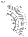
- FIG. 7 is a plan view that shows the principal parts of the table according to the present embodiment.
- FIG. 8 is a schematic drawing for explaining the operation of the table according to the present embodiment.
- FIG. 9 is a schematic diagram for explaining the flow of a gas.
- FIG. 10 is a schematic diagram for explaining the flow of the gas.
- FIG. 11 is a schematic diagram for explaining the flow of the gas.
- FIG. 12A shows the state wherein a transport apparatus holds a rear surface of the substrate.
- FIG. 12B shows the state wherein the transport apparatus holds the rear surface of the substrate.
- FIG. 13 is a flow chart diagram that depicts one example of a process of fabricating a microdevice.
- FIG. 1 is a schematic block diagram that shows the exposure apparatus EX according to the present embodiment.
- the exposure apparatus a comprises a mask stage 3 , which holds a mask M and is movable; a movable substrate stage 4 , which holds a substrate P and is movable; an illumination system IL, which illuminates the mask M held by the mask stage 3 with exposure light EL; a projection optical system PL, which projects an image of a pattern of the mask M that is illuminated by the exposure light EL onto the substrate A; an immersion system 1 , which forms an immersion region LR on an object (e.g., the substrate P) that opposes the projection optical system PL so that an optical path space K of the exposure light EL in the vicinity of the image plane of the projection optical system PL is filled with a liquid LQ; and a control apparatus 7 , which controls the operation of the entire exposure apparatus EX.
- the exposure apparatus EX comprises a transport apparatus 100 that loads and unloads the substrate P to and from the substrate stage
- the substrate P described herein includes one wherein a photosensitive material (photoresist) and a film, such as a protective film, are coated on a base material, e.g., a semiconductor wafer.
- the mask M includes a reticle wherein a device pattern is formed that is reduction projected onto the substrate P.
- a transmitting type mask is used as the mask M in the present embodiment, but a reflection type mask may also be used.
- the illumination system IL illuminates a prescribed illumination area on the mask M with the exposure light EL, which has a uniform luminous flux intensity distribution.
- Examples of light that can be used as the exposure light EL emitted from the illumination system IL include: deep ultraviolet (DUV) light such as bright line (g-line, h-line, or i-line) light emitted from, for example, a mercury lamp and KrF excimer laser light (248 nm wavelength); and vacuum ultraviolet (VUV) light such as ArF excimer laser light (193 nm wavelength) and F 2 laser light (157 nm wavelength).
- DUV deep ultraviolet
- ArF excimer laser light is used as the exposure light EL in the present embodiment.
- the mask stage 3 in the state wherein it holds the mask M, is movable in the X axial, Y axial, and ⁇ Z directions by a mask stage drive apparatus that comprises actuators, e.g., linear motors.
- Laser interferometers 3 L measure the positional information of the mask stage 3 (and, thus, the mask M).
- the laser interferometers 3 L use reflecting surfaces 3 K, which are provided on the mask stage 3 , to measure the positional information of the mask stage 3 .
- the control apparatus 7 controls the mask stage drive apparatus based on the measurement results of the laser interferometers 3 L so as to control the position of the mask M, which is held by the mask stage 3 .
- the reflecting mirrors 3 K need not simply be plane mirrors, but may include corner cubes (retroreflectors); furthermore, it is acceptable to form, for example, reflecting surfaces by minor polishing end surfaces (side surfaces) of the mask stage 3 instead of providing the reflecting mirrors 3 K so that they are fixed to the mask stage 3 .
- the mask stage 3 may be configured so that it is coarsely and finely movable, as disclosed in, for example, Japanese Patent Application Publication No. H8-130179 A (corresponding U.S. Pat. No. 6,721,034).
- the projection optical system PL projects the image of the pattern of the mask M to the substrate P at a prescribed projection magnification and comprises a plurality of optical elements, which are held by a lens barrel PK.
- the projection optical system PL of the present embodiment is a reduction system, the projection magnification of which is, for example, 1 ⁇ 4, 1 ⁇ 5, or 1 ⁇ 8, and forms a reduced image of the pattern of the mask M in a projection region, which is optically conjugate with the illumination area discussed above.
- the projection optical system PL may be a reduction system, a unity magnification system, or an enlargement system.
- an optical axis AX of the projection optical system PL is parallel to the Z axial directions.
- the projection optical system PL may be: a dioptric system that does not include catoptric elements; a catoptric system that does not include dioptic elements; or a catadioptric system that includes both catoptic elements and dioptric elements.
- the projection optical system PL may form either an inverted image or an erect image.
- the substrate stage 4 comprises: a sage main body 4 B; a table 4 T that is mounted on the stage main body 4 B; a tint holder HD 1 that is provided to the table 4 T and detachably holds the substrate P; a plate member T that is disposed so that it surrounds the circumference of the substrate P, which is held by the first holder HD 1 ; and a second holder HD 2 that is provided to the table 4 T and detachably holds the plate member T.
- the stage main body 4 B is noncontactally supported by air bearings 4 A with respect to the upper surface (guide surface) of a base member BP.
- the upper surface of the base member BP is substantially parallel to the XY plane, and the substrate stage 4 is capable of moving on the base member BP in the X and Y directions.
- the substrate stage 4 can be moved on the base member BP by a substrate stage drive apparatus, which comprises actuators such as linear motors, in the state wherein the first holder HD 1 holds the substrate P.
- the substrate stage drive apparatus comprises: a first drive system that is capable of moving the table 4 T, which is mounted on the stage main body 4 B, in the X axial; the Y axial, and the ⁇ Z directions by moving the stage main body 4 B on the base member BP in the X axial, the Y axial, and the ⁇ Z directions; and a second drive system, which is capable of moving the substrate table 4 T in the Z axial, the ⁇ X, and the ⁇ Y directions with respect to the stage main body 4 B.
- the first drive system comprises actuators such as linear motors.
- the second drive system comprises: actuators 4 V, such as voice coil motor; that are interposed between the stage main body 4 B and the table 4 T; and a apparatus (e.g., an encoder; not shown) that measures the amount of drive of each of the actuators 4 V.
- the table 4 T is supported on the stage main body 4 B by at least three actuators 4 V.
- Each of the actuators 4 V is capable of driving the table 4 T with respect to the stage main body 4 B independently in the Z axial directions, and the control apparatus 7 drives the table 4 T with respect to the stage main body 4 B in the Z axial directions, the ⁇ X directions, and the ⁇ Y directions by adjusting the amount of drive of each of the three actuators 4 V.
- the substrate stage drive apparatus which includes the first and second drive systems, is capable of moving the table 4 T of the substrate stage 4 with six degrees of freedom, i.e., in the X axial, the Y axial, the Z axial, the ⁇ X, the ⁇ Y, and the ⁇ Z directions.
- the control apparatus 7 can control the position of the front surface of the substrate P, which is held by the first holder HD 1 of the table 4 T, with six degrees of freedom, i.e., in the X axial, the Y axial, the Z axial, the ⁇ X, the ⁇ Y, and the ⁇ Z directions.
- Laser interferometers 4 L measure the positional information of the table 4 T of the substrate stage 4 (and, in turn, the substrate P).
- the laser interferometers 4 L use reflecting surfaces 4 K, which are provided to the table 4 T, to measure the positional information of the table 4 T in the X axial, the Y axial, and the ⁇ Z directions.
- a focus and level detection system (not shown) detects the surface position information (positional information in the Z arial, the ⁇ X and the ⁇ Y directions) of the front surface of the substrate P, which is held by the first holder HD 1 of the table 4 T.
- the control apparatus 7 controls the substrate stage drive apparatus based on the measurement results of the laser interferometers 4 L and the detection results of the focus and level detection system so as to control the position of the substrate P, which is held by the first holder HD 1 .
- the focus and level detection system detects inclination information (the rotational angle) of the substrate P in the ⁇ X and the ⁇ Y directions by measuring the positional information of the substrate P in the Z axial directions at a plurality of measurement points. Furthermore, if, for example, the laser interferometers 4 L are capable of measuring the positional information of the substrate P in the Z axial, the ⁇ X, and the ⁇ Y directions, then the focus and level detection system does not need to be provided so that the positional information of the substrate P can be measured in the Z axial directions du the exposure operation, and the position of the substrate P in the Z axial, the ⁇ X, and the ⁇ Y directions may be controlled using the measurement results of the laser interferometers 4 L at least dung the exposure operation.
- the immersion system 1 fills the optical path space K of the exposure light EL in the vicinity of the image plane of the projection optical system PL with the liquid LQ.
- the immersion system 1 forms the immersion region LR on the substrate P so that the optical path space K of the exposure light EL between the lower surface of a last optical element FL, which is the optical element of the plurality of optical elements of the projection optical system PL that is closest to the image plane thereof, and the front surface of the substrate P on the substrate stage 4 (the first holder HD 1 ), which is disposed at a position at which it opposes the last optical element FL, is filled with the liquid LQ.
- water pure water
- the immersion system 1 comprises: a nozzle member 70 , which is provided in the vicinity of the optical path space K of the exposure light EL and comprises supply ports 12 , which supply the liquid LQ to the optical path space K, and a recovery port 22 , which recovers the liquid LQ; supply pipes 13 ; a liquid supply apparatus 11 , which supplies the liquid LQ to the supply ports 12 via supply passageways that are formed inside the nozzle member 70 ; and a liquid recovery apparatus 21 , which recovers the liquid LQ that is recovered via the recovery port 22 of the nozzle member 70 via a recovery passageway 24 , which is formed inside the nozzle member 70 , and a recovery pipe 23 .
- the nozzle member 70 is annularly provided so that it surrounds the optical path space K of the exposure light EL.
- the supply ports 12 supply the liquid LQ are provided in the vicinity of the optical path space K of the exposure light EL.
- the recovery port 22 that recovers the liquid LQ is provided to a lower surface of the nozzle member 70 and opposes the front surface of the substrate P, for example, during the exposure of the substrate P.
- the recovery port 22 is provided so that it is further spaced apart from the optical path space K of the exposure light EL than the supply ports 12 are.
- a porous member (mesh) is disposed in the recovery port 22 .
- the liquid supply apparatus 11 comprises: a temperature adjusting apparatus, which adjusts the temperature of the liquid LQ that is to be supplied; a degasifier that reduces a gas component in the liquid LQ; and a filter unit, which eliminates foreign matter in the liquid LQ; in addition, the liquid supply apparatus 11 is capable of feeding the pure, temperature adjusted liquid LQ.
- the liquid recovery apparatus 21 comprises, for example, a vacuum system and is capable of recovering the liquid LQ.
- the control apparatus 7 controls the operation of the immersion system 1 , which includes the liquid supply apparatus 11 and the liquid recovery apparatus 21 .
- the liquid LQ that is fed from the liquid supply apparatus 11 flows through the supply pipes 13 and the supply passageways of the nozzle member 70 , it is supplied to the optical path space K of the exposure light EL via the supply ports 12 .
- the liquid LQ that is recovered via the recovery port 22 by the operation of the liquid recovery apparatus 21 flows through the recovery passageway 24 of the nozzle member 70 , and is then recovered by the liquid recovery apparatus 21 via the recovery pipe 23 .
- the control apparatus 7 forms the immersion region LR of the liquid LQ on the object (e.g., the substrate P) that opposes the last optical element FL so that the optical path space K of the exposure light EL is filled with the liquid LQ by controlling the liquid immersion system 1 so that the liquid supply operation, wherein the liquid supply apparatus 11 is used, and the liquid recovery operation, wherein the liquid recovery apparatus 21 is used, are performed in parallel.
- the exposure apparatus EX projects the image of the pattern of the mask M onto the substrate P, which is held by the first holder HD 1 , by radiating the exposure light EL that passes through the mask M onto the substrate P through the projection optical system PL and the liquid LQ that fills the optical path space K of the exposure light EL, and thereby exposes the substrate P.
- the exposure apparatus EX of the present embodiment employs a local liquid immersion system that, during the exposure of the substrate P, fills the optical path space K of the exposure light EL between the last optical element FL and the substrate P with the liquid LQ, and locally forms the immersion region LR of the liquid LQ, which is larger than the projection region AR of the projection optical system PL and smaller than the substrate P, in part of the area on the substrate P that includes the projection region AR.
- FIG. 2 is a side cross sectional view of the table 4 T in the state wherein the substrate P is held by the first holder HD 1 ;
- FIG. 3 is a plan view, viewed from above, of the table 4 T in the state wherein the substrate P is held by the first holder HD 1 ;
- FIG. 4 is a plan view, viewed from above, of the table 4 T in the state wherein the substrate P is removed from the first holder HD 1 ;
- FIG. 5 is a plan view of the state we the substrate P and the plate member T are removed from the first and second holders HD 1 , HD 2 ;
- FIG. 6 is an enlarged, side cross sectional view of part of the first holder HD 1 ;
- FIG. 7 is a plan view.
- the table 4 T comprises: a base material 30 ; the first holder HD 1 that is provided to the base material 30 and detachably holds the substrate P; and the second holder HD 2 that is provided to the base material 30 and detachably holds the plate member T.
- the plate member T, which is held by the second holder HD 2 is disposed so that it surrounds the circumference of the substrate P, which is held by the first holder HD 1 .
- the first holder HD 1 comprises: first support members 81 that are formed on the base material 30 and support a rear surface of the substrate P; a first circumferential wall 31 that is formed on the base material 30 , is provided so that it surrounds a first space 41 between the base material 30 and the substrate P, which is supported by the fit support members 81 , and has a first upper surface 31 A that opposes the rear surface of the substrate P, which is supported by the first support members 81 ; a second circumferential wall 32 that is formed on the base material 30 , is provided so that it surrounds the first circumferential wall 31 , and has a second upper surface 32 A that opposes the rear surface of the substrate P, which is supported by the first support members 81 ; a third circumferential wall 33 that is formed on the base material 30 , is provided so that it surrounds the first support members 81 and the second circumferential wall 32 , and has a third upper surface 33 A
- the first circumferential wall 31 is ring shaped (substantially circular) and is substantially the same shape as the external shape of the substrate P.
- the first upper surface 31 A of the first circumferential wall 31 is provided so that it opposes an area that is relatively close to the circumferential edge of the rear surface of the substrate P, which is supported by the first support members 81 .
- the first space 41 which is enclosed by the rear surface of the substrate P, the first circumferential wall 31 , and the base material 30 , is formed at the rear surface side of the substrate P, which is held by the first holder HD 1 .
- the second circumferential wall 32 is formed along and at the outer (lateral) side of the first circumferential wall 31 with respect to the first space 41 .
- the first circumferential wall 31 and the second circumferential wall 32 are spaced apart by a prescribed spacing (e.g., 1 mm).
- the second circumferential wall 32 is also ring shaped (substantially circular) and is substantially the same shape as the external shape of the substrate P.
- the second upper surface 32 A of the second circumferential wall 32 is provided so that it opposes an area that is relatively close to de circumferential edge of the rear surface of the substrate P, which is supported by the first support members 81 .
- the second space 42 which is enclosed by the rear rice of the substrate the first circumferential wall 31 , the second circumferential wall 32 , and the base material 30 , is formed at the rear surface side of the substrate P, which is held by the first holder HD 1 .
- the third circumferential wall 33 is formed at the outer side of the first circumferential wall 31 and the second circumferential wall 32 with respect to the first space 41 so that it is spaced apart from the second circumferential wall 32 by a prescribed distance.
- the third circumferential wall 33 is also ring shaped (substantially circular) and is substantially the same shape as external shape of the substrate P.
- the third upper surface 33 A of the third circumferential wall 33 is provided so that it opposes a circumferential edge area (edge area) of the rear surface of the substrate P, which is supported by the first support members 81 .
- the third space 43 which is enclosed by the rear surface of the substrate P, the second circumferential wall 32 , the third circumferential wall 33 , and the base material 30 , is formed at the rear surface side of the substrate P, which is held by the first holder HD 1 .
- first, second, and third circumferential walls 31 , 32 , 33 are all provided so that they oppose the edge area of the rear surface of the substrate P, which is supported by the first support members 81 , or an area that is close to that edge area.
- the first, second, and third circumferential walls 31 , 32 , 33 are disposed so that they are substantially concentric.
- the first holder HD 1 holds the substrate P so that the center of the first space 41 and the center of the rear surface of the substrate P substantially coincide.
- the outer diameter of the third circumferential wall 33 is smaller than that of the substrate.
- the third circumferential wall 33 is provided at the inner (medial) side of the edge (i.e., at the center side) of the substrate P, which is supported by the first support members 81 .
- Part of the edge area of the substrate P, which is supported by the first support members 81 hangs over the outer side of the third circumferential wall 33 by a prescribed amount.
- au overhang area H 1 (refer to FIG. 6 ).
- the width of the overhang area H 1 is approximately 1.5 mm.
- a first gap G 1 is formed between the rear surface of the substrate P, which is supported by the first holder HD 1 , and the first upper surface 31 A of the first circumferential wall 31 .
- a second gap G 2 is formed between the rear surface of the substrate P, which is supported by the first holder HD 1 , and the second upper surface 32 A of the second circumferential wall 32 .
- the third circumferential wall 33 is formed so that the rear surface of the substrate P, which is supported by the first holder HD 1 , and the third upper surface 33 A contact one another.
- the first gap G 1 and the second gap G 2 are each approximately 2-10 ⁇ m.
- the width of each of the first, second, and third upper surfaces 31 A, 32 A, 33 A is approximately 0.5 mm.
- the fluid flow ports 60 are connected to the second space 42 .
- multiple fluid flow ports 60 are formed in the base material 30 between the first circumferential wall 31 and the second circumferential wall 32 at prescribed intervals in the circumferential directions at the outer side of the first circumferential wall 31 so that they surround the first circumferential wall 31 , as shown in FIG. 4 , FIG. 5 , FIG. 7 , and the like.
- each of the fluid flow ports 60 is circular, but may be polygonal.
- the fluid flow ports 60 are disposed so that they are substantially equispaced.
- the second space 42 and the exterior space are connected via the fluid flow ports 60 .
- the gas can circulate between the second space 42 and the exterior space via the fluid flow ports 60 and a passageway 60 R, which is connected to the fluid flow ports 60 .
- the second space 42 is open to the atmosphere via the fluid flow ports 60 .
- annular first groove 51 is formed in the base material 30 between the first circumferential wall 31 and the second circumferential wall 32 and along and at the outer side of the first circumferential wall 31 so that it surrounds the first circumferential wall 31 .
- the fluid flow ports 60 are formed on the inner side of the first groove 51 (in a bottom part of the first groove 51 ).
- the first suction ports 61 which are formed between the second circumferential wall 32 of the base material 30 and the third circumferential wall 33 , are connected to a first suction apparatus 91 , which comprises a vacuum system and the like, via a passageway 61 R.
- the first suction ports 61 are connected to the third space 43 .
- the control apparatus 7 drives the first suction apparatus 91 in order to suction the fluid (including at least one of the gas and the liquid) from the third space 43 .
- first suction ports 61 are formed in the base material 30 between the second circumferential wall 32 and the third circumferential wall 33 at prescribed intervals in the circumferential directions at the outer side of the second circumferential wall 32 so that they surround the second circumferential wall 32 .
- each of the first suction ports 61 is circular, but may be polygonal.
- the first suction ports 61 are disposed so that they are substantially equispaced.
- annular second groove 52 is formed in the base material 30 between the second circumferential wall 32 and the third circumferential wall 33 along the second circumferential wall 32 so that it surrounds the second circumferential wall 32 .
- the first suction ports 61 are formed on the inner side of the second groove 52 (in the bottom part of the second groove 52 ).
- the first support members 81 are pin shaped projecting parts that are formed on the upper surface of the base material 30 , and multiple first port members 81 are disposed at prescribed positions of the upper surface of the base material 30 .
- the plurality of the first support members 81 is disposed at the inner side of the first circumferential wall 31 .
- the plurality of the first support members 81 is disposed between the second circumferential wall 32 and the second groove 52 and between the second groove 52 and the third circumferential wall 33 .
- the first support members 81 inside the third space 43 are not shown for the sake of simplicity. However, if the flatness of the front surface Pa of the substrate P can be ensured sufficiently, then the first support members 81 do not have to be provided in the third space 43 .
- Multiple second suction ports 62 which suction the fluid principally gas) in order to negatively pressurize the first space 41 and the third space 43 with respect to the atmospheric pressure, are provided in the base material 30 .
- the second suction ports 62 are provided at the inner side of the first circumferential wall 31 and between the second circumferential wall 32 and the third circumferential wall 33 .
- the second suction ports 62 are used solely to chuck the substrate P.
- the second suction ports 62 are formed at the inner side of the first circumferential wall 31 at a plurality of prescribed positions that are different than the positions of the first support members 81 .
- the second suction ports 62 are formed between the second circumferential wall 32 and the third circumferential wall 33 at positions that are more spaced apart from the second circumferential wall 32 than the first suction ports 61 are.
- the multiple second suction ports 62 are provided in the upper surface of the base material 30 between the second circumferential wall 32 and the third circumferential wall 33 at prescribed positions between the second groove 52 and the third circumferential wall 33 , and are not provided between the second circumferential wall 32 and the second groove 52 .
- the second suction ports 62 which are provided between the second groove 52 and the third circumferential wall 33 , are not shown for the sake of simplicity.
- the second suction ports 62 between the second groove 52 and the third circumferential wall 33 do not have to be provided if the flatness of the front surface Pa of the substrate P can be sufficiently ensured solely by the second suction ports 62 provided at the inner side of the first circumferential wall 31 , and the substrate P can be held so that it is does not move.
- the second suction ports 62 are connected to a second suction apparatus 92 , which comprises a vacuum system and the like, via a passageway 62 R, and are connected to the first space 41 and the third space 43 .
- the control apparatus 7 can suction the fluid (including at least one of the gas and the liquid) from the first and third spaces 41 , 43 by operating the second suction apparatus 92 .
- the control apparatus 7 negatively pressurizes the first space 41 and the third space 43 by operating the second suction apparatus 92 so as to suction the gas from the first space 41 , which is enclosed by the rear surface of the substrate P, the first circumferential wall 31 , and the base material 30 , as well as the fluid (principally gas) from the third space 43 , which is enclosed by the rear surface of the substrate P, the second circumferential wall 32 , the third circumferential wall 33 , and the base material 30 ; thereby, the substrate P is chucked to the first support members 81 .
- the substrate P can be removed from the first holder HD 1 by canceling the suction operation that is performed by the second suction apparatus 92 .
- the substrate P can be chucked to and dechucked from the first holder HD 1 by controlling the suction operation wherein the second suction ports 62 are used.
- the first holder HD 1 in the present embodiment is part of a so-called pin chuck mechanism.
- the table 4 T comprises: a fourth circumferential wall 34 that is formed at the base material 30 , is provided so that it surrounds the third circumferential wall 33 , and has a fourth upper surface 34 A that opposes the rear surface of the substrate P, which is supported by the first support members 81 ; and third suction ports 63 , which suction the fluid from the space between the third circumferential wall 33 and the fourth circumferential wall 34 .
- the fourth circumferential wall 34 is formed at the outer side of the third circumferential wall 33 with respect to the third space 43 , and is spaced apart from the third circumferential wall 33 by a prescribed distance.
- the fourth circumferential wall 34 is formed along the third circumferential wall 33 .
- the fourth circumferential wall 34 is also ring shaped (substantially circular) and is substantially the same shape as the external shape of the substrate P. However, as described below, the fourth circumferential wall 34 in the present embodiment is not formed continuously, and comprises a plurality of arcuate circumferential wall parts.
- the fourth upper surface 34 A of the fourth circumferential wall 34 opposes the overhang area H 1 of the rear surface of the substrate P, which is supported by the first support members 81 .
- a fourth gap G 4 is formed between the overhang area H 1 of the rear surface of the substrate P, which is supported by the first support members 81 , and the fourth upper surface 34 A of the fourth circumferential wall 34 .
- the fourth gap G 4 is set to, for example, approximately 1-10 ⁇ m.
- the width of the fourth upper surface 34 A is set to approximately 0-5 mm.
- the third suction ports 63 are connected to a third suction apparatus 93 , which comprises a vacuum system and the like, via a passageway 63 R.
- the third suction ports 63 are connected to a fourth space 44 between the third circumferential wall 33 and the fourth circumferential wall 34 .
- the fourth space 44 is enclosed by the overhang area H 1 of the rear surface of the substrate P, the third circumferential wall 33 , the fourth circumferential wall 34 , and the base material 30 .
- the control apparatus 7 is capable of suctioning the fluid (at least one of the gas and the liquid) of the fourth space 44 by operating the third suction apparatus 93 .
- multiple third suction ports 63 are formed in the base material 30 between the third circumferential wall 33 and the fourth circumferential wall 34 at the outer side of the third circumferential wall 33 at prescribed intervals in the circumferential directions so that they surround the third circumferential wall 33 .
- the third suction ports 63 are circular, but may be polygonal.
- the third suction ports 63 in the present embodiment are disposed along the third circumferential wall 33 at substantially equal intervals.
- annular third groove 53 is formed in the base material 30 between the third circumferential wall 33 and the fourth circumferential wall 34 and along and at the outer side of the third circumferential wall 33 so that it surrounds the third circumferential wall 33 .
- the third suction ports 63 are formed on the inner side of the third groove 53 (in the bottom part of the third groove 53 ).
- slits 37 are formed in parts of the fourth circumferential wall 34 .
- the slits 37 are formed at prescribed positions in the circumferential directions of the fourth circumferential wall 34 .
- the slits 37 are disposed at substantially equal intervals in the circumferential directions of the fourth circumferential wall 34 .
- the slits 37 are formed so that they extend in the vertical directions (the Z axial directions), and the lower ends thereof reach the base material 30 . Moreover, the upper ends of the slits 37 reach the fob upper surface 34 A of the fourth circumferential wall 34 .
- the fourth circumferential wall 34 in the present embodiment is configured by a combination of multiple protruding pan which are arcuate in a plan view; in addition, the provision of these arcuate protruding parts along the third circumferential wall 33 forms a substantially ring shape as a whole.
- third suction ports 63 are disposed between adjacent slits 37 .
- two third suction ports 63 are disposed between adjacent slits 37 .
- each of the fluid flow ports 60 is disposed between adjacent first suction ports 61 .
- the fluid flow ports 60 and the first suction ports 61 are provided at different positions in the circumferential directions. Imagining a set of straight lines that extend radially from the center of the first space 41 , which is circular in a plan view, the fluid flow ports 60 and the first suction ports 61 are disposed at positions such that none of the fluid flow ports 60 and the first suction ports 61 are formed along the same straight line.
- the plate member T and the second holder HD 2 which detachably holds the plate member T.
- the plate member T is a member that is separate from the table 4 T, and is detachable with respect to the base material 30 .
- a substantially circular hole JA in which the substrate P can be disposed, is formed at the center part of the plate member T.
- the plate member T, which is held by the second holder HD 2 is disposed so that it surrounds the substrate P, which is held by the first holder HD 1 .
- the front surface of the plate member T which is held by the second holder HD 2 is a flat surface that is configured so that it is substantially the same height as (flush with) the front surface of the substrate P, which is held by the first holder HD 1 . Furthermore, there may be a level difference between the front surface of the substrate P, which is held by the first holder HD 1 , and the front surface of the plate member T, which is held by the second holder HD 2 .
- a fifth gap G 5 is formed between the edge (outer side surface) of the substrate P, which is held by the first holder HD 1 , and the edge (inner side surface) on the inner side of the plate member-T, which is held by the second holder HD 2 .
- the fifth gap 65 is set to, for example, approximately 0.1-10 nm.
- the external shape of the plate member T is rectangular in a plan view and is substantially the same shape as the external shape of the base material 30 in the present embodiment.
- the plate member T is liquid repellent with respect to the liquid LQ.
- the plate member T is made of a liquid repellent material, e.g., a fluororesin such as polytetrafluoroethylene (TeflonTM), or an acrylic resin.
- the plate member T may be formed from, for example, a metal, and its surface may be coated with a liquid repellent material such as a fluororesin.
- the second holder HD 2 comprises second support members 82 that are formed on the base material 30 and support the rear surface of the plate member T.
- the second holder HD 2 comprises: a fifth circumferential wall 35 that is formed on the base material 30 , is provided so that it surrounds the fourth circumferential wall 34 , and has a fifth upper surface 35 A that opposes the rear spice of the plate member T, which is supported by the second support members 82 , and a sixth circumferential wall 36 that is formed on the base material 30 , is provided so that it surrounds the fifth circumferential wall 35 , and has a sixth upper surface 36 A that opposes the rear surface of the plate member T, which is supported by the second support members 82 .
- the second support members 82 are formed on the base material 30 between the fifth circumferential wall 35 and the sixth circumferential wall 36 .
- the fifth upper surface 35 A of the fifth circumferential wall 35 is provided so that it opposes an inner edge area (edge area onto inner side) of the rear surface of the plate member T, which is supported by the second support members 82 , in the vicinity of the hole TH.
- the sixth upper surface 36 A of the circumferential wall 36 is provided so that it opposes an outer edge area (edge area on the outer side) of the rear surface of the plate member T, which is supported by the second support members 82 .
- a fifth space 45 which is enclosed by the rear surface of the plate member T, the fifth circumferential wall 35 , the sixth circumferential wall 36 , and the base material 30 , is formed at the rear surface side of the plate member T, which is held by the second holder HD 2 .
- the plate member T is supported on the second support members 82 of the second holder HD 2 by negatively pressuring the fifth space 45 .
- the fifth circumferential wall 35 is formed so that the rear surface of the plate member T, which is supported by the second support members 82 , and the fifth upper surface 35 A contact one another.
- the sixth circumferential wall 36 is formed so that the rear surface of the plate member T, which is supported byte second support members 82 , and the sixth upper surface 36 A contact one another.
- the second support members 82 are pin shaped projecting parts that are formed on the upper surface of the base material 30 and are disposed at multiple prescribed positions on the upper surface of the base material 30 between the fifth circumferential wall 35 and the sixth circumferential wall 36 .
- Fourth suction ports 64 which suction the fluid (principally gas) from the interior of the fifth space 45 in order to negatively pressurize the fifth space 45 , are provided in the base mal 30 between the fifth circumferential wall 35 and to sixth circumferential wall 36 .
- the fourth suction ports 64 are used solely to chuck the plate member T.
- the fourth suction ports 64 are formed in the base material 30 between the fifth circumferential wall 35 and the sixth circumferential wall 36 at prescribed positions that are different than the positions of the second support members 82 .
- the fourth suction ports 64 are connected to the fifth space 45 and to a fourth suction apparatus 94 , which comp a vacuum system and the like, via a passageway 64 R.
- the control apparatus 7 is capable of suctioning the fluid (at least one of the gas and the liquid) of the fifth space 45 by operating the fourth suction apparatus 94 .
- the control apparatus 7 negatively pressurizes the fifth spa 45 by operating the fourth suction apparatus 94 so as to suction the fluid (principally gas) from the fifth space 45 , which is enclosed by the rear surface of the plate member T supported by the second support members 82 , the fifth circumferential wall 35 , the sixth circumferential wall 36 , and the base material 30 ; thereby, the plate member T is chucked to the second support members 82 .
- the plate member T can be chucked to and dechucked from the second holder HD 2 by controlling the suction operation wherein the fourth suction ports 64 are used.
- the second holder HD 2 is part of the so-called pin chuck mechanism.
- a sixth space 46 that is enclosed by the overhang area H 1 of the rear surface of the substrate P supported by the first support members 81 , the fourth circumferential wall 34 , the fifth circumferential wall 35 , and the base material 30 , is connected to the exterior space (the atmospheric space) via the fifth gap G 5 that is formed between the substrate P, which is supported by the first support members 81 , and the plate member T, which is supported by the second support members 82 .
- the fourth space 44 is connected to the external space via the fourth gap G 4 , the fifth gap G 5 , and the slits 37 .
- the fluid at least one of the gas and the liquid
- the fourth space 44 can circulate between the fourth space 44 and the exterior space via the slits 37 , the fourth gap G 4 , and the fifth gap G 5 .
- a sixth gap G 6 of approximately 1 mm is formed between the outer side surface of the third circumferential wall 33 and the inner side surface of the fourth circumferential wall 34 .
- a seventh gap G 7 of approximately 1 mm is formed between the outer side surface of the fourth circumferential wall 34 and the inner side surface of the fifth circumferential wall 35 .
- the control apparatus 7 disposes the substrate stage 4 at a prescribed substrate exchange position (loading position) and uses the transport apparatus 100 to load the substrate P, which is to undergo an exposing process, on the first holder HD 1 of the table 4 T of the substrate stage 4 .
- the control apparatus 7 uses the first support members 81 to chuck the substrate P by driving the second suction apparatus. 92 with a prescribed timing so as to negatively pressurize the first space 41 and the third space 43 via the second suction ports 62 .
- the control apparatus 7 drives the fourth suction apparatus 94 so as to negatively pressurize the fifth space 45 via the fourth suction ports 64 , and thereby the plate member T is held by the second holder HD 2 .
- control apparatus 7 starts the suction operation, wherein the first suction ports 61 are used, by driving the first suction apparatus 91 with a prescribed timing.
- the control apparatus 7 performs (continues) the suction operation, wherein the first suction ports 61 are used, while the immersion region LR is formed on at least one of the front surface of the subsume P and the front surface of the plate member T.
- the control apparatus 7 loads the substrate P on the first holder HD 1 ; immediately thereafter, starts the suction operation wherein the second suction ports 62 are used and, simultaneously therewith, starts the suction operation wherein the first suction ports 61 are used; exposes the substrate P, which is held by the first holder HD 1 ; and then continues the suction operation, wherein the first suction ports 61 are used, until immediately before the substrate P is unloaded from the first holder HD 1 after the exposure is complete. Furthermore, the suction operation, wherein the first suction ports 61 are used, may be started after the performance of the suction operation, wherein the second suction ports 62 are used, and the substrate P is held by the first holder HD 1 .
- the suction operation when the first suction ports 61 are used should be started before the immersion region LR is formed on at least part of the upper surface of the substrate P and the upper surface of the plate member T.
- the control apparatus 7 uses the immersion system 1 to form the immersion region LR of the liquid LQ on the substrate P in order to perform an immersion exposure on the substrate P, which is held by the first holder HD 1 .
- the control apparatus 7 exposes the substrate P, which is held by the first holder HD 1 of the table 4 T, through the liquid LQ of the immersion region LR.
- the immersion region LR of the liquid LQ is formed above the fifth gap G 5 .
- the fifth gap G 5 is set to 0.1-1.0 mm, which prevents the liquid LQ from leaking into the fifth gap G 5 caused by the surface tension of the liquid LQ.
- the plate member T is made liquid repellent which prevents the liquid LQ from leaking to the rear surface side of the substrate P via the fifth gap G 5 . Accordingly, the liquid LQ can be held below the projection optical system PL even if the area in the vicinity of the edge of the front surface of the substrate P is exposed.
- the liquid LQ is prevented from leaking via theft gap G 5 by, for example, reducing the size of the fifth gap G 5 and disposing the liquid repellent plate member T so that it surrounds the substrate P, there is a possibility that the liquid LQ will leak via the fifth gap G 5 , which is formed around the substrate P, because of, for example, pressure changes in the liquid LQ that forms the immersion region LR.
- the control apparatus 7 does not perform the suction operation, wherein the third suction ports 63 are used, at least during the exposure of the substrate P. Namely, the control apparatus 7 stops the operation of the third suction apparatus 93 at least during the exposure of the substrate P.
- the table 4 T of the present embodiment is configured so that it is difficult for the liquid LQ to leak into the space at the inner side of the third circumferential wall 33 even if the liquid LQ leaks into the fourth space 44 . Nevertheless, there is a possibility that the liquid LQ will leak into the space at the inner side of the third circumferential wall 33 as a result of the state wherein a rear surface of the substrate P and the upper surface 33 A of the third circumferential wall 33 contact one another.
- the fluid flow ports 60 which are capable of supplying the gas, are provided at the inner side of the third circumferential wall 33 , the first suction ports 61 are provided between the third circumferential wall 33 and the fluid flow ports 60 , and the suction operation, wherein the first suction ports 61 are used, is performed, which makes it possible to prevent the liquid LQ from leaking into the first space 41 and the second space 42 even if the liquid LQ were to leak into the space at the inner side of the third circumferential wall 33 .
- FIG. 8 schematically shows the state wherein the suction operation, wherein the first suction ports 61 are used, is performed.
- the suction operation wherein the first suction ports 61 are used, makes it possible to generate gas flows F 2 that flow from the second space 42 toward the third space 43 via the second gap G 2 .
- the second space 42 is open to the atmosphere via the fluid flow ports 60 ; consequently, by performing the suction operation wherein the first suction ports 61 are used, the gas is supplied (flows) from the exterior space (the atmospheric space) into the second space 42 via the fluid flow ports 60 ; thereby, it is possible to generate the gas flows F 2 that flow from the second space 42 toward the first suction ports 61 of the third space 43 via the second gap G 2 .
- the width of the second gap G 2 is optimized in order to generate the gas flows F 2 in the desired state.
- the second gap G 2 is 2-10 ⁇ m, which makes it possible to generate the gas flows F 2 that flow from the second space 42 toward the third space 43 at a high speed.
- the second gap G 2 is minute, i.e., approximately 2-10 ⁇ m, and the flow volume per unit of time of the gas that flows from the second space 42 into the third space 43 is optimized. Accordingly, the gas that flows from the second space 42 into the third space 43 presents virtually no obstacle to the negative pressurization of the third space 43 , thereby making it possible for the first holder HD 1 to perform the vacuum chucking operation smoothly. Namely, the second gap G 2 is optimized so that it is possible to generate the gas flows F 2 in the desired state and to use the first holder HD 1 to chuck the substrate P.
- the first gap G 1 is formed between the rear surface of the substrate P and the first upper surface 31 A of the first circumferential wall 31 , and thereby it is possible to prevent, for example, local deformation of the substrate P from occurring as a result of; for example, the contact between the first circumferential wall 31 and the substrate P.
- the first space 41 is negatively pressurized by the suction operation wherein the second suction ports 62 are used, and therefore a gas flow F 1 is also generated that flows from the second space 42 toward the first space 41 via the first gap G 1 ; however, the first gap G 1 is also optimized so that it is possible to generate the gas flow F 1 in the desired state and to use the fit holder HD 1 to vacuum chuck the substrate P.
- the gas that is supplied (that flows) from the fluid flow ports 60 in the second space 42 flows toward the second gap G 2 as it is guided to the first groove 51 and spreads in the circumferential directions. Namely, the speed and volume of the flow of the gas that is supplied from the fluid flow ports 60 to the second space 42 toward the second gap G 2 are uniformized in the circumferential directions by the first groove 51 .
- the second upper surface 32 A of the second circumferential wall 32 is annular, and the second gap G 2 is substantially the same in the circumferential directions of the second upper surface 32 A. Accordingly, the speed and volume of the flow of the gas that flows from the second space 42 to the third space 43 are uniformized over the entire area of the second gap G 2 .
- first suction ports 61 are formed at prescribed intervals in the circumferential directions at the outer side of the second circumferential wall 32 so that they surround the second circumferential wall 32 .
- first suction ports 61 are formed inside the second groove 52 , which is annularly formed so that it surrounds the second circumferential wall 32 .
- the gas that is supplied (that flows) from the second space 42 into the third space 43 flows toward the first suction ports 61 along the second groove 52 as it is guided to the second groove 52 and spreads in the circumferential directions.
- the gas flows F 2 that flow from the second space 42 toward the third space 43 via the second gap G 2 are uniformized in the circumferential directions.
- flows of the gas toward each of the first suction ports 61 are generated along the second groove 52 . Accordingly, even if the liquid LQ leaks into the third space 43 at the inner side of the third circumferential wall 33 from any portion between the rear surface of the substrate P, which is supported by the first support members 81 , and the third upper surface 33 A of the third circumferential wall 33 , the liquid LQ that does so is drawn inside the second groove 52 and can be recovered via the first suction ports 61 . As a result, it is possible to prevent that liquid LQ from reaching the space (the first space 41 and the second space 42 ) at the inner side of the second circumferential wall 32 .
- the control apparatus 7 stops the suction operation of the second suction apparatus 92 .
- the control apparatus 7 stops the suction operation of the second suction apparatus 92 , it continues the suction operation of the first suction apparatus 91 for a prescribed time, and then stops the suction operation of the first suction apparatus 91 . Stopping the suction operation of the first suction apparatus 91 after the suction operation of the second suction apparatus 92 is stopped makes it possible to prevent the liquid LQ inside the passageway 61 R, which is connected to the first suction apparatus 91 , from flowing in reverse and jetting out from the first suction ports 61 .
- the control apparatus 7 drives the third suction apparatus 93 in the state wherein the substrate P is held by the first holder HD 1 and starts the suction operation, wherein the third suction ports 63 are used, before stopping the suction operation of the second suction apparatus 92 .
- the control apparatus 7 performs the suction operation wherein the third suction ports 63 are used, which makes it possible to recover the liquid LQ that adheres to the overhang area H 1 of the rear surface of the substrate P and the liquid LQ that is present in the fourth space 44 .
- the control apparatus 7 recovers the liquid LQ that leaks into via the fifth gap G 5 by driving the third suction apparatus 93 for the prescribed time.
- the fourth gap G 4 which is formed between the fourth upper surface 34 A of the fourth circumferential wall 34 and the overhang area H 1 of the rear surface of the substrate P, forms a passageway through which the gas can circulate between the fourth space 44 and the exterior space. As shown in FIG.
- the third suction apparatus 93 suctions the fluid (principally gas) from the fourth space 44 via the third suction ports 63 , and thereby the fluid flows from the exterior space (the atmospheric space) into the fourth space 44 via the fifth gap G 5 and the fourth gap G 4 , and gas flows F 3 are generated that flow toward the third suction ports 63 .
- the slits 37 which are provided to pats of the fourth circumferential wall 34 , also form passageways through which the gas can circulate between the fourth space 44 and the exterior space. As shown in FIG.
- the third suction apparatus 93 suctions the fluid (principally gas) from the fourth space 44 via the third suction ports 63 , and therefore the fluid flows from the exterior space (the atmospheric space) into the fourth space 44 via the fifth gap G 5 and the slits 37 , and gas flows F 4 are generated toward the third suction ports 63 .
- the gas flows F 3 , F 4 which are generated by the suction operation wherein the third suction ports 63 are used, move the liquid LQ that adheres to the overhang area H 1 of the rear surface of the substrate P and the liquid LQ that leaks into the fourth space 44 (the liquid LQ that adheres to, for example, the outer side surface of the third circumferential wall 33 , the inner side surface of the fourth circumferential wall 34 , and the upper surface of the base material 30 ) to the third suction ports 63 where it is recovered via the third suction ports 63 .
- multiple third suction ports 63 are formed at prescribed intervals so that they surround the third circumferential wall 33 .
- the third suction ports 63 are formed inside the third groove 53 , which is annularly formed, so that they surround the third circumferential wall 33 .
- the gas that is supplied (that flows) from the slits 37 and the fourth gap G 4 into the fourth space 44 flows toward the third suction ports 63 while it is being guided to the third groove 53 , the outer side surface of the third circumferential wall 33 , and the inner side surface of the fourth circumferential wall 34 . Accordingly, it is possible to use the third suction ports 63 to recover the liquid LQ that is present in the fourth space 44 smoothly.
- the suction operation is performed after the exposure of the substrate P through the liquid LQ is complete. Stopping the suction operation, wherein the third suction ports 63 are used, during the exposure makes it possible to prevent vibrations caused by the suction operation (liquid recovery operation) wherein the third suction ports 63 , as well as to prevent a deterioration in the degree of flatness of the front surface of the substrate P. In addition, performing the suction operation, wherein the third suction ports 63 are used, in the state wherein the substrate P is held by the first holder HD 1 makes it possible to recover the liquid LQ smoothly.
- the suction operation (liquid recovery operation), wherein the third suction ports 63 are used, may be performed at any time provided it is after the exposure of the substrate P is complete and before the substrate P is unloaded from the first holder HD 1 . Furthermore, the suction operation, wherein the third suction ports 63 are used, may be performed during the exposure of the substrate P provided that there is no problem with, for example, vibrations, the flatness of the substrate P, or the heat of vaporization.
- control apparatus 7 stops the suction operation of the second suction apparatus 92 during the suction operation of the third suction apparatus 93 . Furthermore, after the operation, wherein the third suction ports 63 are used, of recovering the liquid from the fourth space 44 has continued for the prescribed time, the control apparatus 7 stops the suction operation of the first suction apparatus 91 and thereafter stops the suction operation of the third suction apparatus 93 . Thereby, it is possible to reliably prevent the liquid LQ from flowing from the fourth space 44 into the third space 43 at the inner side of the third circumferential wall 33 .
- the suction operations of the first suction apparatus 91 and the third suction apparatus 93 may be stopped simultaneously, or the suction operation of the first suction apparatus 91 may be stopped after the suction operation of the third suction apparatus 93 is stopped, provided that it is after the operation of recovering the liquid LQ from the fourth space 44 has been performed sufficiently.
- the control apparatus 7 uses a substrate lifting mechanism (not shown) to lift the substrate P off of the first: holder HD 1 and uses the port apparatus 100 to unload the substrate P from the first holder HD 1 at the prescribed substrate exchange position.
- FIGS. 12A and 12B show the state wherein the substrate P, which was unloaded from the first holder HD 1 , is transported by the transported apparatus 100 .
- the transport apparatus 100 comprises an arm member 101 and protruding members 102 , each of which is provided on the arm member 101 and has a contact surface 103 that contacts a prescribed area PA in the vicinity of the center of the rear surface of the substrate P.
- the first space 41 of the first holder HD 1 is set in accordance with the prescribed area PA of the rear surface of the substrate P that contacts the contact surfaces 103 of the transport apparatus 100 .
- the suction operation prevents the liquid LQ from leaking into the first space 41 and the second space 42 , and from adhering to the prescribed area PA on the rear surface of the substrate P. Accordingly, bringing the contact surfaces 103 of the transport apparatus 100 into contact with the prescribed area PA on the rear surface of the substrate P makes it possible to prevent the liquid LQ from adhering to the transport 100 .
- the gas flows F 2 which flow from the second space 42 toward the third space 43 via the second gap G 2 , are generated, and thereby it is possible to prevent the liquid LQ from adhering to the prescribed area PA (the area that corresponds to the first space 41 ) on the rear surface of the substrate P. Accordingly, it is possible to prevent the liquid LQ from adhering to the transport apparatus 100 even if the transport apparatus 100 contacts the prescribed area PA on the rear surface of the substrate P.
- the liquid LQ that adheres to the overhang area H 1 of the substrate P is recovered by the suction operation wherein the third suction ports 63 are used, which makes it possible to prevent the liquid LQ from scattering along the transport pathway even while that substrate P is being transported after it has been unloaded.
- providing an eliminating apparatus that is capable of eliminating the liquid LQ that adheres to the substrate P as needed along the path on which the substrate P is transported after it has been unloaded from the substrate stage 4 makes it possible to prevent the liquid LQ from scattering along the transport pathway.
- the eliminating apparatus may resupply the liquid LQ onto the substrate P and subsequently eliminate the liquid LQ that adheres to the substrate P.
- the first support members 81 are disposed between the second circumferential wall 32 and the second groove 52 as well as between the second groove 52 and the third circumferential wall 33 , thereby making it possible to support the substrate P satisfactorily while preventing, for example, the substrate P from warping.
- the second suction ports 62 are not disposed in the third space 43 between the second circumferential wall 32 and the first suction ports 61 (the first groove 51 ).
- the second suction ports 62 are not disposed in the third space 43 between the second circumferential wall 32 and the first suction ports 61 (the first groove 51 ).
- the second suction ports 62 that are provided at the inner side of the first circumferential wall 31 and the second suction ports that are provided between the second circumferential wall 32 and the third circumferential wall 33 may be connected to separate suction apparatuses (vacuum pumps and the like), and the suction operation, wherein the second suction ports 62 that are provided between the second circumferential wall 32 and the third circumferential wall 33 are used, may be started after the start of the suction operation wherein the second suction ports 62 that are provided at the inner side of the first circumferential wall 31 are used.
- one end of the passageway 62 R may be connected to a connection port that is provided at the inner side of the first circumferential wall 31 , and the suction operation, wherein the second suction ports 62 that are provided between the second circumferential wall 32 and the third circumferential wall 33 are used, may be performed via the connection port and the second suction ports 62 that are provided at the inner side of the first circumferential wall 31 .
- a gas supply apparatus which comprises a pressure pump and the like, may be connected to the fluid flow ports 60 and may be used to supply gas actively to the second space 42 via the fluid flow ports 60 .
- the fluid flow ports 60 may be formed at prescribed positions on the upper surface of the base material 30 without forming the first groove 51 , provided that an even, desired flow of gas can be generated by optimizing, for example, the arrangement, number, and shapes of the fluid flow ports 60 .
- the second groove 52 and the third groove 53 may be omitted and the first suction ports 61 and the third suction ports 63 can be formed at prescribed positions on the upper surface of the base material 30 , provided that the desired gas flows can be generated.
- the second circumferential wall 32 may be omitted, provided that the gas flows F 2 that flow from the fluid flow ports 60 to the first suction ports 61 can be formed with a uniform speed and volume of flow by providing numerous fluid flow ports 60 in the circumferential directions.
- the first gap G 1 is formed between the first upper surface 31 A of the first circumferential wall 31 and the rear surface of the substrate P, but the first upper surface 31 A of the first circumferential wall 31 and the rear surface of the substrate P may contact one another.
- At least one annular circumferential wall may be additionally provided at the inner side of the first circumferential wall 31 so that a prescribed gap is formed between that additional wall and the rear surface of the substrate P.
- the second space 42 is open to the atmosphere, and therefore there is a possibility that the negative pressure (chucking force) in the first space 41 may be insufficient; however, the addition of the at least one annular circumferential wall at the inner side of the first circumferential wall 31 makes it possible to maintain strong chucking force at the space at the inner side of that added circumferential wall.
- the chucking force at the space at the inner side of the added circumferential wall is stronger than the chucking force at the space at the outer side thereof, which makes it possible to bold the substrate P stably.
- the fluid flow ports ( 60 ), which are capable of supplying the gas to the first holder HD 1 , and the suction ports ( 61 ), which recover the liquid LQ that flows thereinto, are provided in order to recover the liquid LQ that flows into the space at the inner side of the third circumferential wall 33 ; however, fluid flow ports that are capable of supplying the gas to the second holder HD 2 and suction ports that recover the liquid LQ that flows thereinto may be provided in order to recover the liquid LQ that leaks into the space at the inner side of the fifth circumferential wall 35 (the fifth space 45 at the rear surface side of the plate member T).
- the flat part around the substrate P is formed by the detachable plate member T, but it may be formed by a member that is integral to the base material 30 .
- the optical path space at the image plane side of the last optical element is filled with the liquid, but it is possible to adopt a projection optical system wherein the optical path space at the object plane side of the last optical element is also filled with the liquid, as disclosed in PCT International Publication WO2004/019128.
- the liquid LQ in the present embodiment is water, it may be a liquid other than water; for example, if the light source of the exposure light EL is an F 2 laser, the light of which does not transmit through water, then it is acceptable to use a fluorine based fluid that is capable of transmitting F 2 a light, such as perfluorinated polyether (PFPE) or fluorine based oil, as the liquid LQ.
- PFPE perfluorinated polyether
- portions that contact the liquid LQ are lyophilically treated by forming a tins film with, for example, a substance that has a molecular structure that contains fluorine or the like and has low polarity.
- liquid LQ a liquid (e.g., cedar oil) that is transparent to the exposure light EL, has the highest possible refractive index, and is stable with respect to the projection optical system PL and the photoresist that is coated on the front surface of the substrate P.
- a liquid e.g., cedar oil
- liquid LQ a liquid that has a refractive index of approximately 1.6 to 1.8
- liquids that can be used as the liquid LQ include: a prescribed liquid that has an O—H bond or a C—H bond such as isopropanol, which has a refractive index of approximately 1.50, or glycerol (glycerin), which has a refractive index of approximately 1.61; a prescribed liquid (organic solvent) such as hexane, heptane, or decane; and a prescribed liquid such as decalin or bicyclohexyl.
- a prescribed liquid that has an O—H bond or a C—H bond such as isopropanol, which has a refractive index of approximately 1.50, or glycerol (glycerin), which has a refractive index of approximately 1.61
- a prescribed liquid (organic solvent) such as hexane, heptane, or decane
- a prescribed liquid such as decalin
- the liquid LQ may be a liquid wherein a base, such as H + , Cs + , K + , Cl ⁇ , SO 4 2 ⁇ , PO 4 2 ⁇ , or an acid is added to (mixed with) pure water.
- the liquid LQ may be a liquid wherein fine particles of aluminum oxide or the like are added to (mixed with) pure water.
- the liquid LQ preferably has a small light absorption coefficient, low temperature dependency, and is stable with respect to the photosensitive material (a protective film such as a topcoat film, an antireflection film, or the like) that is coated on the projection optical system PL and/or the front surface of the substrate P.
- a protective film such as a topcoat film, an antireflection film, or the like
- the optical element LS 1 can be formed from, for example, quart (silica). Alternatively, it may be formed from a monocrystalline fluorine compound material such as calcium fluoride (fluorite), barium fluoride, strontium fluoride, lithium fluoride, sodium fluoride, and BaLiF 3 . Furthermore, the last optical element FL may be formed from lutetium aluminum garnet (LuAG).
- At least one of the optical elements of the projection optical system FL may be formed from a material that has a refractive index that is hiker than that of quartz and/or fluorite (e.g., 1.6 or greater).
- a material that has a refractive index that is hiker than that of quartz and/or fluorite e.g., 1.6 or greater.
- sapphire, germanium dioxide, or the like as disclosed in PCT International Publication WO2005/059617, or potassium chloride (which has a refractive index of approximately 1.75) or the like as disclosed in PCT International Publication WO2005/059618.
- the substrate P in each of the abovementioned embodiments is not limited to a semiconductor wafer for fabricating semiconductor devices; for example, a glass substrate for a display device, a ceramic wafer for a thin film magnetic head, or the original plate of a mask or a reticle (synthetic quartz, silicon wafer) that is used by an exposure apparatus can be employed as the substrate P.
- the shape of the substrate P is not limited to a circle, and may be another shape, e.g., a rectangle.
- the exposure apparatus EX may also be adapted to a step-and-scan type scanning exposure apparatus (a scanning stepper) that scans and exposes the pattern of the mask M while synchronously moving the mask M and the substrate P, as well as to a step-and-repeat type projection exposure apparatus (a stepper) that performs full field exposure of the pattern of the mask M with the mask M and the substrate P in a stationary state, and sequentially steps the substrate P.
- a scanning stepper that scans and exposes the pattern of the mask M while synchronously moving the mask M and the substrate P
- a step-and-repeat type projection exposure apparatus a stepper
- the exposure apparatus EX can also be adapted to an exposure apt that uses a projection optical system (e.g., a dioptric projection optical system that does not include a catoptric element and has a 1 ⁇ 8 reduction magnification) to expose the substrate P with a reduced image of the full field of a first pattern in a state wherein the first patter and the substrate P are substantially stationary.
- a projection optical system e.g., a dioptric projection optical system that does not include a catoptric element and has a 1 ⁇ 8 reduction magnification
- it can also be adapted to a stitching type full-field exposure apparatus that subsequently further uses that projection optical system to expose the substrate P with a reduced image of the full field of a second pattern, in a state wherein the second pattern and the substrate P are substantially stationary, so that the second pattern partially overlaps the first pattern.
- the stitching type exposure apparatus can also be adapted to a step-and-stitch type exposure apparatus that transfers at least two patterns onto the substrate P so that they are
- the present invention can also be adapted to a multistage type exposure apparatus that is provided with a plurality of substrate stages, as disclosed in for example, Japanese Patent Application Publication No. H10-163099A, Japanese Patent Application Publication No. H10-214783A, Published Japanese Translation No. 2000-505958 of the PCT International Publication, U.S. Pat. Nos. 6,341,007, 6,400,441, 6,549,269, 6,590,634, 6,208,407, and U.S. Pat. No. 6,262,796.
- the present invention can also be adapted to an exposure apparatus that is provided with a substrate stage that holds the substrate and a measurement stage whereon a fiducial member (wherein a fiducial mark is formed) and various photoelectric sensors are mounted, as disclosed in Japanese Patent Application Publication No. H11-135400A, Japanese Patent Application Publication No. 2000-164504A, and U.S. Pat. No. 6,897,963.
- positional information about the mask stage and the substrate stage are each measured using an interferometer system, but the present invention is not limited thereto and, for example, an encoder system may be used that detects a scale (diffraction grating) that is provided to the upper surface of the substrate stage.
- an encoder system may be used that detects a scale (diffraction grating) that is provided to the upper surface of the substrate stage.
- the position of the substrate stage may be controlled by switching between the interferometer system and the encoder system, or by using both.
- each of the abovementioned embodiments explained an example of an exposure apparatus that comprises a projection optical system that has a plurality of optical elements, but a projection optical system that comprises one optical element may be used.
- the present invention can be adapted to an exposure apparatus and an exposing method wherein a projection optical system is not used. Even if a projection optical system is not used, exposure light is radiated to the substrate through an optical member, such as a mask or a lens, and an immersion region is formed in a prescribed space between the substrate and such an optical member.
- the type of exposure apparatus EX is not limited to a semiconductor device fabrication exposure apparatus that exposes the pattern of a semiconductor device on the substrate P, but can also be widely adapted to exposure apparatuses that are used for fabricating, for example, liquid crystal devices or displays, and exposure apparatuses that are used for fabricating thin film magnetic heads, image capturing devices (CCDs), micromachines (MEMS), DNA chips, or reticles and masks.
- exposure apparatuses that are used for fabricating, for example, liquid crystal devices or displays, and exposure apparatuses that are used for fabricating thin film magnetic heads, image capturing devices (CCDs), micromachines (MEMS), DNA chips, or reticles and masks.
- a light transmitting type mask is used wherein a probed shielding pattern (or a phase pattern or a dimming pattern) is formed on a light transmitting substrate; however, instead of such a mask, it is also possible to use an electronic mask wherein a transmittance pattern, a reflected patter, or a light emitting pattern is formed based on electronic data of the pattern to be exposed, as disclosed in, for example, U.S. Pat. No. 6,778,257; here, an electronic mask, which is also called a viable forming mask includes, for example, a digital micromirror device (DMD), which is one type of a non light emitting image display device (a spatial light modulator).
- DMD digital micromirror device
- the present invention can also be adapted to an exposure apparatus (a lithographic system) that exposes the substrate P with a line-and-space pattern.
- the present invention can also be adapted to an exposure apparatus that combines, through a projection optical system, the patterns of two masks on a substrate, and double exposes, substantially simultaneously, a single shot region on that substrate with a single scanning exposure, as disclosed in, for example, Published Japanese Translation No. 2004-519850 of the PCT International Publication (corresponding U.S. Pat. No. 6,611,316).
- the exposure apparatus EX is manufactured by assembling various subsystems, including each constituent element, so that prescribed mechanical, electrical, and optical accuracies as maintained. To ensure these various accuracies, adjustments are performed before and after this assembly, including an adjustment to achieve optical accuracy for the various optical systems, an adjustment to achieve mechanical accuracy for the various mechanical systems, and an adjustment to achieve electrical accuracy for the various electrical systems.
- the process of assembling the exposure apparatus EX from the various subsystems includes, for example, the mechanical interconnection of the various subsystems, the wiring and connection of electrical circuits, and the piping and connection of the atmospheric pressure circuit.
- the process of assembling the exposure apparatus EX from the various subsystems is complete, a comprehensive adjustment is performed to ensure the various accuracies of the exposure apparatus EX as a whole. Furthermore, it is preferable to manufacture the exposure apparatus EC in a clean room wherein, for example, the temperature and the cleanliness level are controlled.
- a micro-device such as a semiconductor device, is manufactured by, for example: a step 201 that designs the functions and performance of the micro-device; a step 202 that fabricates a mask (reticle) based on this designing step; a step 203 that fabricates a substrate, which is the base material of the device; a step 204 that includes substrate treatment processes, such as the process of exposing the pattern of the mask onto the substrate by using the exposure apparatus EX of the embodiments discussed above, a process that develops the exposed substrate, and a process that heats (cures) and etches the developed substrate; a device assembling step 205 (comprising a dicing process, a bonding process, and a packaging process); and an inspecting step 206 .
- a step 201 that designs the functions and performance of the micro-device
- a step 202 that fabricates a mask (reticle) based on this designing step
- a step 203 that fabricates a substrate, which is the
Applications Claiming Priority (3)
| Application Number | Priority Date | Filing Date | Title |
|---|---|---|---|
| JP2005354463 | 2005-12-08 | ||
| JP2005-354463 | 2005-12-08 | ||
| PCT/JP2006/324552 WO2007066758A1 (ja) | 2005-12-08 | 2006-12-08 | 基板保持装置、露光装置、露光方法、及びデバイス製造方法 |
Related Parent Applications (1)
| Application Number | Title | Priority Date | Filing Date |
|---|---|---|---|
| PCT/JP2006/324552 Continuation WO2007066758A1 (ja) | 2005-12-08 | 2006-12-08 | 基板保持装置、露光装置、露光方法、及びデバイス製造方法 |
Publications (2)
| Publication Number | Publication Date |
|---|---|
| US20080239275A1 US20080239275A1 (en) | 2008-10-02 |
| US8089615B2 true US8089615B2 (en) | 2012-01-03 |
Family
ID=38122903
Family Applications (1)
| Application Number | Title | Priority Date | Filing Date |
|---|---|---|---|
| US12/155,514 Expired - Fee Related US8089615B2 (en) | 2005-12-08 | 2008-06-05 | Substrate holding apparatus, exposure apparatus, exposing method, and device fabricating method |
Country Status (7)
| Country | Link |
|---|---|
| US (1) | US8089615B2 (ja) |
| EP (3) | EP1962329B1 (ja) |
| JP (1) | JP4968076B2 (ja) |
| KR (3) | KR101704310B1 (ja) |
| HK (2) | HK1123627A1 (ja) |
| TW (2) | TWI538014B (ja) |
| WO (1) | WO2007066758A1 (ja) |
Cited By (5)
| Publication number | Priority date | Publication date | Assignee | Title |
|---|---|---|---|---|
| US20100013169A1 (en) * | 2008-07-17 | 2010-01-21 | Bjorn Monteen | Thin wafer chuck |
| US20100133735A1 (en) * | 2008-11-28 | 2010-06-03 | Canon Kabushiki Kaisha | Substrate holding apparatus, substrate holding method, exposure apparatus, and device manufacturing method |
| US20110241298A1 (en) * | 2010-04-01 | 2011-10-06 | Topcon 3D Inspection Laboratories Inc. | Wafer flattening apparatus and method |
| US20170345702A1 (en) * | 2016-05-26 | 2017-11-30 | Ngk Spark Plug Co., Ltd. | Substrate holding device and method of manufacturing the same |
| US11056378B2 (en) * | 2019-01-07 | 2021-07-06 | Disco Corporation | Workpiece holding method and workpiece processing method |
Families Citing this family (30)
| Publication number | Priority date | Publication date | Assignee | Title |
|---|---|---|---|---|
| EP2270597B1 (en) | 2003-04-09 | 2017-11-01 | Nikon Corporation | Exposure method and apparatus and device manufacturing method |
| TWI569308B (zh) | 2003-10-28 | 2017-02-01 | 尼康股份有限公司 | 照明光學裝置、曝光裝置、曝光方法以及元件製造 方法 |
| TWI385414B (zh) | 2003-11-20 | 2013-02-11 | 尼康股份有限公司 | 光學照明裝置、照明方法、曝光裝置、曝光方法以及元件製造方法 |
| TWI609410B (zh) | 2004-02-06 | 2017-12-21 | 尼康股份有限公司 | 光學照明裝置、曝光裝置、曝光方法以及元件製造方法 |
| KR101524964B1 (ko) | 2005-05-12 | 2015-06-01 | 가부시키가이샤 니콘 | 투영 광학계, 노광 장치 및 노광 방법 |
| US8451427B2 (en) | 2007-09-14 | 2013-05-28 | Nikon Corporation | Illumination optical system, exposure apparatus, optical element and manufacturing method thereof, and device manufacturing method |
| JP5267029B2 (ja) | 2007-10-12 | 2013-08-21 | 株式会社ニコン | 照明光学装置、露光装置及びデバイスの製造方法 |
| WO2009050976A1 (en) | 2007-10-16 | 2009-04-23 | Nikon Corporation | Illumination optical system, exposure apparatus, and device manufacturing method |
| CN101681125B (zh) | 2007-10-16 | 2013-08-21 | 株式会社尼康 | 照明光学系统、曝光装置以及元件制造方法 |
| US8379187B2 (en) | 2007-10-24 | 2013-02-19 | Nikon Corporation | Optical unit, illumination optical apparatus, exposure apparatus, and device manufacturing method |
| US9116346B2 (en) | 2007-11-06 | 2015-08-25 | Nikon Corporation | Illumination apparatus, illumination method, exposure apparatus, and device manufacturing method |
| CN101910817B (zh) | 2008-05-28 | 2016-03-09 | 株式会社尼康 | 照明光学系统、曝光装置以及器件制造方法 |
| JP5517171B2 (ja) * | 2009-11-25 | 2014-06-11 | Nskテクノロジー株式会社 | 露光ユニット及び基板の露光方法 |
| NL2009189A (en) | 2011-08-17 | 2013-02-19 | Asml Netherlands Bv | Support table for a lithographic apparatus, lithographic apparatus and device manufacturing method. |
| US9835957B2 (en) | 2013-09-27 | 2017-12-05 | Asml Netherlands B.V. | Support table for a lithographic apparatus, lithographic apparatus and device manufacturing method |
| US10527092B2 (en) | 2014-10-23 | 2020-01-07 | Asml Netherlands B.V. | Support table for a lithographic apparatus, method of loading a substrate, lithographic apparatus and device manufacturing method |
| CN107004574B (zh) * | 2014-12-12 | 2020-06-30 | 佳能株式会社 | 基板保持装置、光刻设备以及物品制造方法 |
| JP6496255B2 (ja) * | 2016-01-29 | 2019-04-03 | 日本特殊陶業株式会社 | 基板保持装置 |
| NL2018051A (en) | 2016-02-08 | 2017-08-11 | Asml Netherlands Bv | Lithographic apparatus, method for unloading a substrate and method for loading a substrate |
| US10534271B2 (en) * | 2017-01-26 | 2020-01-14 | Asml Netherlands B.V. | Lithography apparatus and a method of manufacturing a device |
| JP6946134B2 (ja) * | 2017-09-27 | 2021-10-06 | 日本特殊陶業株式会社 | 基板保持部材および基板保持方法 |
| CN111213093A (zh) * | 2017-10-12 | 2020-05-29 | Asml荷兰有限公司 | 用于在光刻设备中使用的衬底支架 |
| EP3707747A4 (en) | 2017-11-10 | 2021-07-28 | Applied Materials, Inc. | DOUBLE-SIDED PATTERN CHUCK |
| CN113075865B (zh) * | 2020-01-06 | 2022-11-08 | 夏泰鑫半导体(青岛)有限公司 | 一种用于处理半导体衬底的装置和方法 |
| KR102405676B1 (ko) | 2022-02-24 | 2022-06-08 | 주식회사 필라이즈 | 인공지능 기반의 맞춤형 건강기능식품 추천 정보를 제공하는 방법, 장치 및 시스템 |
| KR102405675B1 (ko) | 2022-02-24 | 2022-06-08 | 주식회사 필라이즈 | 인공지능 기반의 맞춤형 건강기능식품 상태 및 복용 정보를 제공하는 방법, 장치 및 시스템 |
| KR102405673B1 (ko) | 2022-02-24 | 2022-06-08 | 주식회사 필라이즈 | 인공지능 기반의 개인화된 건강기능식품 정보를 제공하는 방법, 장치 및 시스템 |
| KR102405677B1 (ko) | 2022-02-24 | 2022-06-08 | 주식회사 필라이즈 | 인공지능을 이용한 이미지 인식 기반 맞춤형 건강기능식품 정보를 제공하는 방법, 장치 및 시스템 |
| KR102405674B1 (ko) | 2022-02-24 | 2022-06-08 | 주식회사 필라이즈 | 인공지능을 이용한 코호트 분석 기반 건강기능식품 정보 제공 방법, 장치 및 시스템 |
| KR102545551B1 (ko) | 2022-11-16 | 2023-06-21 | 주식회사 바디버디 | 인공지능 기반 맞춤형 건강기능식품 큐레이션 서비스 제공 방법, 장치 및 시스템 |
Citations (33)
| Publication number | Priority date | Publication date | Assignee | Title |
|---|---|---|---|---|
| JPH08130179A (ja) | 1994-11-01 | 1996-05-21 | Nikon Corp | ステージ装置 |
| JPH10163099A (ja) | 1996-11-28 | 1998-06-19 | Nikon Corp | 露光方法及び露光装置 |
| JPH10214783A (ja) | 1996-11-28 | 1998-08-11 | Nikon Corp | 投影露光装置及び投影露光方法 |
| US5850280A (en) | 1994-06-16 | 1998-12-15 | Nikon Corporation | Stage unit, drive table, and scanning exposure and apparatus using same |
| JPH11135400A (ja) | 1997-10-31 | 1999-05-21 | Nikon Corp | 露光装置 |
| WO1999049504A1 (fr) | 1998-03-26 | 1999-09-30 | Nikon Corporation | Procede et systeme d'exposition par projection |
| US5969441A (en) | 1996-12-24 | 1999-10-19 | Asm Lithography Bv | Two-dimensionally balanced positioning device with two object holders, and lithographic device provided with such a positioning device |
| JP2000164504A (ja) | 1998-11-30 | 2000-06-16 | Nikon Corp | ステージ装置、露光装置、及び前記ステージ装置を用いた位置決め方法 |
| US6208407B1 (en) | 1997-12-22 | 2001-03-27 | Asm Lithography B.V. | Method and apparatus for repetitively projecting a mask pattern on a substrate, using a time-saving height measurement |
| WO2001035168A1 (en) | 1999-11-10 | 2001-05-17 | Massachusetts Institute Of Technology | Interference lithography utilizing phase-locked scanning beams |
| US6262796B1 (en) | 1997-03-10 | 2001-07-17 | Asm Lithography B.V. | Positioning device having two object holders |
| US6341007B1 (en) | 1996-11-28 | 2002-01-22 | Nikon Corporation | Exposure apparatus and method |
| WO2002069049A2 (en) | 2001-02-27 | 2002-09-06 | Asml Us, Inc. | Simultaneous imaging of two reticles |
| WO2004019128A2 (en) | 2002-08-23 | 2004-03-04 | Nikon Corporation | Projection optical system and method for photolithography and exposure apparatus and method using same |
| US6721034B1 (en) | 1994-06-16 | 2004-04-13 | Nikon Corporation | Stage unit, drive table, and scanning exposure apparatus using the same |
| US6778257B2 (en) | 2001-07-24 | 2004-08-17 | Asml Netherlands B.V. | Imaging apparatus |
| JP2004289127A (ja) | 2002-11-12 | 2004-10-14 | Asml Netherlands Bv | リソグラフィ装置およびデバイス製造方法 |
| WO2004093160A2 (en) | 2003-04-10 | 2004-10-28 | Nikon Corporation | Run-off path to collect liquid for an immersion lithography apparatus |
| WO2004112108A1 (ja) | 2003-06-13 | 2004-12-23 | Nikon Corporation | 露光方法、基板ステージ、露光装置、及びデバイス製造方法 |
| US6897963B1 (en) | 1997-12-18 | 2005-05-24 | Nikon Corporation | Stage device and exposure apparatus |
| US20050122505A1 (en) | 2003-12-08 | 2005-06-09 | Canon Kabushiki Kaisha | Substrate-holding technique |
| WO2005059618A2 (en) | 2003-12-19 | 2005-06-30 | Carl Zeiss Smt Ag | Microlithography projection objective with crystal lens |
| WO2005059617A2 (en) | 2003-12-15 | 2005-06-30 | Carl Zeiss Smt Ag | Projection objective having a high aperture and a planar end surface |
| US20050219499A1 (en) | 2004-04-01 | 2005-10-06 | Asml Netherlands B.V. | Lithographic apparatus and device manufacturing method |
| US20050219488A1 (en) | 2002-12-10 | 2005-10-06 | Nikon Corporation | Exposure apparatus and method for producing device |
| JP2005310933A (ja) | 2004-04-20 | 2005-11-04 | Nikon Corp | 基板保持部材、露光装置及びデバイス製造方法 |
| WO2006077859A1 (ja) * | 2005-01-18 | 2006-07-27 | Nikon Corporation | 液体除去装置、露光装置、及びデバイス製造方法 |
| US20070146665A1 (en) * | 2005-12-27 | 2007-06-28 | Asml Netherlands B.V. | Lithographic apparatus and substrate edge seal |
| US20070177125A1 (en) | 2004-06-09 | 2007-08-02 | Nikon Corporation | Substrate holding unit, exposure apparatus having same, exposure method, method for producing device, and liquid repellent plate |
| US20070269294A1 (en) | 2004-09-17 | 2007-11-22 | Nikon Corporation | Substrate Holding Device, Exposure Apparatus, and Device Manufacturing Method |
| US20080043210A1 (en) | 2004-06-21 | 2008-02-21 | Nikon Corporation | Exposure Apparatus and Device Manufacturing Method |
| US20080202555A1 (en) * | 2006-09-08 | 2008-08-28 | Nikon Corporation | Cleaning member, cleaning method, and device manufacturing method |
| US20090135382A1 (en) * | 2005-04-28 | 2009-05-28 | Nikon Corporation | Exposure method, exposure apparatus, and method for producing device |
Family Cites Families (5)
| Publication number | Priority date | Publication date | Assignee | Title |
|---|---|---|---|---|
| JP3312164B2 (ja) * | 1995-04-07 | 2002-08-05 | 日本電信電話株式会社 | 真空吸着装置 |
| KR20010045963A (ko) | 1999-11-09 | 2001-06-05 | 박종섭 | 반도체 소자의 캐패시터 제조방법 |
| JP4529433B2 (ja) | 2002-12-10 | 2010-08-25 | 株式会社ニコン | 露光装置及び露光方法、デバイス製造方法 |
| JP2004310933A (ja) * | 2003-04-09 | 2004-11-04 | Sony Corp | ディスクドライブ装置 |
| TW201816844A (zh) * | 2004-03-25 | 2018-05-01 | 日商尼康股份有限公司 | 曝光裝置、曝光方法、及元件製造方法 |
-
2006
- 2006-12-08 KR KR1020157002535A patent/KR101704310B1/ko active IP Right Grant
- 2006-12-08 TW TW102119096A patent/TWI538014B/zh not_active IP Right Cessation
- 2006-12-08 KR KR1020087016430A patent/KR101340138B1/ko active IP Right Grant
- 2006-12-08 KR KR1020137021783A patent/KR101539517B1/ko active IP Right Grant
- 2006-12-08 JP JP2007549191A patent/JP4968076B2/ja active Active
- 2006-12-08 EP EP06834307.8A patent/EP1962329B1/en not_active Not-in-force
- 2006-12-08 TW TW095146184A patent/TWI406321B/zh not_active IP Right Cessation
- 2006-12-08 WO PCT/JP2006/324552 patent/WO2007066758A1/ja active Application Filing
- 2006-12-08 EP EP14166620.6A patent/EP2768016B1/en not_active Not-in-force
- 2006-12-08 EP EP17195426.6A patent/EP3327759A1/en not_active Withdrawn
-
2008
- 2008-06-05 US US12/155,514 patent/US8089615B2/en not_active Expired - Fee Related
-
2009
- 2009-01-07 HK HK09100117.9A patent/HK1123627A1/xx not_active IP Right Cessation
-
2015
- 2015-01-02 HK HK15100027.0A patent/HK1199771A1/xx not_active IP Right Cessation
Patent Citations (45)
| Publication number | Priority date | Publication date | Assignee | Title |
|---|---|---|---|---|
| US6721034B1 (en) | 1994-06-16 | 2004-04-13 | Nikon Corporation | Stage unit, drive table, and scanning exposure apparatus using the same |
| US5850280A (en) | 1994-06-16 | 1998-12-15 | Nikon Corporation | Stage unit, drive table, and scanning exposure and apparatus using same |
| JPH08130179A (ja) | 1994-11-01 | 1996-05-21 | Nikon Corp | ステージ装置 |
| JPH10163099A (ja) | 1996-11-28 | 1998-06-19 | Nikon Corp | 露光方法及び露光装置 |
| JPH10214783A (ja) | 1996-11-28 | 1998-08-11 | Nikon Corp | 投影露光装置及び投影露光方法 |
| US6590634B1 (en) | 1996-11-28 | 2003-07-08 | Nikon Corporation | Exposure apparatus and method |
| US6400441B1 (en) | 1996-11-28 | 2002-06-04 | Nikon Corporation | Projection exposure apparatus and method |
| US6549269B1 (en) | 1996-11-28 | 2003-04-15 | Nikon Corporation | Exposure apparatus and an exposure method |
| US6341007B1 (en) | 1996-11-28 | 2002-01-22 | Nikon Corporation | Exposure apparatus and method |
| US5969441A (en) | 1996-12-24 | 1999-10-19 | Asm Lithography Bv | Two-dimensionally balanced positioning device with two object holders, and lithographic device provided with such a positioning device |
| JP2000505958A (ja) | 1996-12-24 | 2000-05-16 | コーニンクレッカ フィリップス エレクトロニクス エヌ ヴィ | 2個の物品ホルダを有する二次元バランス位置決め装置及びこの位置決め装置を有するリソグラフ装置 |
| US6262796B1 (en) | 1997-03-10 | 2001-07-17 | Asm Lithography B.V. | Positioning device having two object holders |
| JPH11135400A (ja) | 1997-10-31 | 1999-05-21 | Nikon Corp | 露光装置 |
| US6897963B1 (en) | 1997-12-18 | 2005-05-24 | Nikon Corporation | Stage device and exposure apparatus |
| US6208407B1 (en) | 1997-12-22 | 2001-03-27 | Asm Lithography B.V. | Method and apparatus for repetitively projecting a mask pattern on a substrate, using a time-saving height measurement |
| WO1999049504A1 (fr) | 1998-03-26 | 1999-09-30 | Nikon Corporation | Procede et systeme d'exposition par projection |
| JP2000164504A (ja) | 1998-11-30 | 2000-06-16 | Nikon Corp | ステージ装置、露光装置、及び前記ステージ装置を用いた位置決め方法 |
| WO2001035168A1 (en) | 1999-11-10 | 2001-05-17 | Massachusetts Institute Of Technology | Interference lithography utilizing phase-locked scanning beams |
| WO2002069049A2 (en) | 2001-02-27 | 2002-09-06 | Asml Us, Inc. | Simultaneous imaging of two reticles |
| US6611316B2 (en) | 2001-02-27 | 2003-08-26 | Asml Holding N.V. | Method and system for dual reticle image exposure |
| JP2004519850A (ja) | 2001-02-27 | 2004-07-02 | エイエスエムエル ユーエス, インコーポレイテッド | デュアルレチクルイメージを露光する方法および装置 |
| US6778257B2 (en) | 2001-07-24 | 2004-08-17 | Asml Netherlands B.V. | Imaging apparatus |
| WO2004019128A2 (en) | 2002-08-23 | 2004-03-04 | Nikon Corporation | Projection optical system and method for photolithography and exposure apparatus and method using same |
| JP2004289127A (ja) | 2002-11-12 | 2004-10-14 | Asml Netherlands Bv | リソグラフィ装置およびデバイス製造方法 |
| US7199858B2 (en) | 2002-11-12 | 2007-04-03 | Asml Netherlands B.V. | Lithographic apparatus and device manufacturing method |
| US20050219488A1 (en) | 2002-12-10 | 2005-10-06 | Nikon Corporation | Exposure apparatus and method for producing device |
| WO2004093160A2 (en) | 2003-04-10 | 2004-10-28 | Nikon Corporation | Run-off path to collect liquid for an immersion lithography apparatus |
| US20060139614A1 (en) * | 2003-06-13 | 2006-06-29 | Nikon Corporation | Exposure method, substrate stage, exposure apparatus, and device manufacturing method |
| EP1641028A1 (en) | 2003-06-13 | 2006-03-29 | Nikon Corporation | Exposure method, substrate stage, exposure apparatus and method for manufacturing device |
| WO2004112108A1 (ja) | 2003-06-13 | 2004-12-23 | Nikon Corporation | 露光方法、基板ステージ、露光装置、及びデバイス製造方法 |
| JP2005175016A (ja) | 2003-12-08 | 2005-06-30 | Canon Inc | 基板保持装置およびそれを用いた露光装置ならびにデバイス製造方法 |
| US20050122505A1 (en) | 2003-12-08 | 2005-06-09 | Canon Kabushiki Kaisha | Substrate-holding technique |
| WO2005059617A2 (en) | 2003-12-15 | 2005-06-30 | Carl Zeiss Smt Ag | Projection objective having a high aperture and a planar end surface |
| WO2005059618A2 (en) | 2003-12-19 | 2005-06-30 | Carl Zeiss Smt Ag | Microlithography projection objective with crystal lens |
| US20050219499A1 (en) | 2004-04-01 | 2005-10-06 | Asml Netherlands B.V. | Lithographic apparatus and device manufacturing method |
| JP2005310933A (ja) | 2004-04-20 | 2005-11-04 | Nikon Corp | 基板保持部材、露光装置及びデバイス製造方法 |
| US20070177125A1 (en) | 2004-06-09 | 2007-08-02 | Nikon Corporation | Substrate holding unit, exposure apparatus having same, exposure method, method for producing device, and liquid repellent plate |
| US20080043210A1 (en) | 2004-06-21 | 2008-02-21 | Nikon Corporation | Exposure Apparatus and Device Manufacturing Method |
| US20070269294A1 (en) | 2004-09-17 | 2007-11-22 | Nikon Corporation | Substrate Holding Device, Exposure Apparatus, and Device Manufacturing Method |
| WO2006077859A1 (ja) * | 2005-01-18 | 2006-07-27 | Nikon Corporation | 液体除去装置、露光装置、及びデバイス製造方法 |
| US20080165330A1 (en) * | 2005-01-18 | 2008-07-10 | Nikon Corporation | Liquid Removing Apparatus, Exposure Apparatus and Device Fabricating Method |
| US20090135382A1 (en) * | 2005-04-28 | 2009-05-28 | Nikon Corporation | Exposure method, exposure apparatus, and method for producing device |
| US20070146665A1 (en) * | 2005-12-27 | 2007-06-28 | Asml Netherlands B.V. | Lithographic apparatus and substrate edge seal |
| US20080202555A1 (en) * | 2006-09-08 | 2008-08-28 | Nikon Corporation | Cleaning member, cleaning method, and device manufacturing method |
| US20100195068A1 (en) * | 2006-09-08 | 2010-08-05 | Yuichi Shibazaki | Cleaning member, cleaning method, and device manufacturing method |
Non-Patent Citations (3)
| Title |
|---|
| International Search Report mailed on Mar. 6, 2007 in corresponding PCT Application No. PCT/JP2006/324552. (with English language translation). |
| Search report mailed on May 9, 2011 in corresponding European Application No. 06834307.8. |
| Written Opinion mailed on Mar. 6, 2007 in corresponding PCT Application No. PCT/JP2006/324552. (with English language translation). |
Cited By (9)
| Publication number | Priority date | Publication date | Assignee | Title |
|---|---|---|---|---|
| US20100013169A1 (en) * | 2008-07-17 | 2010-01-21 | Bjorn Monteen | Thin wafer chuck |
| US8336188B2 (en) * | 2008-07-17 | 2012-12-25 | Formfactor, Inc. | Thin wafer chuck |
| US20100133735A1 (en) * | 2008-11-28 | 2010-06-03 | Canon Kabushiki Kaisha | Substrate holding apparatus, substrate holding method, exposure apparatus, and device manufacturing method |
| US20110241298A1 (en) * | 2010-04-01 | 2011-10-06 | Topcon 3D Inspection Laboratories Inc. | Wafer flattening apparatus and method |
| US8695990B2 (en) * | 2010-04-01 | 2014-04-15 | Nidec-Read Corporation | Wafer flattening apparatus and method |
| US20170345702A1 (en) * | 2016-05-26 | 2017-11-30 | Ngk Spark Plug Co., Ltd. | Substrate holding device and method of manufacturing the same |
| TWI694539B (zh) * | 2016-05-26 | 2020-05-21 | 日商日本特殊陶業股份有限公司 | 基板保持裝置及其製造方法 |
| US10755959B2 (en) * | 2016-05-26 | 2020-08-25 | Ngk Spark Plug Co., Ltd. | Substrate holding device and method of manufacturing the same |
| US11056378B2 (en) * | 2019-01-07 | 2021-07-06 | Disco Corporation | Workpiece holding method and workpiece processing method |
Also Published As
| Publication number | Publication date |
|---|---|
| EP1962329A1 (en) | 2008-08-27 |
| TW200737298A (en) | 2007-10-01 |
| TWI406321B (zh) | 2013-08-21 |
| KR101704310B1 (ko) | 2017-02-07 |
| KR20130105920A (ko) | 2013-09-26 |
| EP2768016B1 (en) | 2017-10-25 |
| EP1962329A4 (en) | 2011-06-08 |
| KR20150023915A (ko) | 2015-03-05 |
| HK1123627A1 (en) | 2009-06-19 |
| JPWO2007066758A1 (ja) | 2009-05-21 |
| KR20080075906A (ko) | 2008-08-19 |
| EP3327759A1 (en) | 2018-05-30 |
| KR101340138B1 (ko) | 2013-12-10 |
| JP4968076B2 (ja) | 2012-07-04 |
| TW201342427A (zh) | 2013-10-16 |
| EP2768016A1 (en) | 2014-08-20 |
| TWI538014B (zh) | 2016-06-11 |
| WO2007066758A1 (ja) | 2007-06-14 |
| HK1199771A1 (en) | 2015-07-17 |
| US20080239275A1 (en) | 2008-10-02 |
| KR101539517B1 (ko) | 2015-07-24 |
| EP1962329B1 (en) | 2014-08-06 |
Similar Documents
| Publication | Publication Date | Title |
|---|---|---|
| US8089615B2 (en) | Substrate holding apparatus, exposure apparatus, exposing method, and device fabricating method | |
| US9964860B2 (en) | Substrate holding apparatus, exposure apparatus, and device fabricating method | |
| US8004651B2 (en) | Liquid recovery system, immersion exposure apparatus, immersion exposing method, and device fabricating method | |
| US8345217B2 (en) | Liquid recovery member, exposure apparatus, exposing method, and device fabricating method | |
| US7927428B2 (en) | Cleaning member, cleaning method, and device manufacturing method | |
| US8134685B2 (en) | Liquid recovery system, immersion exposure apparatus, immersion exposing method, and device fabricating method | |
| US8508714B2 (en) | Exposure apparatus, exposure method, and method for producing device | |
| US20100045949A1 (en) | Exposure apparatus, maintaining method and device fabricating method | |
| US20080239256A1 (en) | Exposure apparatus, exposing method, and device fabricating method | |
| US8013975B2 (en) | Exposure apparatus, exposure method, and method for producing device | |
| US8040490B2 (en) | Liquid immersion exposure apparatus, exposure method, and method for producing device | |
| US8654306B2 (en) | Exposure apparatus, cleaning method, and device fabricating method | |
| WO2008059916A1 (fr) | Appareil et procédé d'exposition et procédé de fabrication de dispositif | |
| US8451425B2 (en) | Exposure apparatus, exposure method, cleaning apparatus, and device manufacturing method |
Legal Events
| Date | Code | Title | Description |
|---|---|---|---|
| AS | Assignment |
Owner name: NIKON CORPORATION, JAPAN Free format text: ASSIGNMENT OF ASSIGNORS INTEREST;ASSIGNORS:MIZUTANI, TAKEYUKI;SHIBAZAKI, YUICHI;SHIBUTA, MAKOTO;REEL/FRAME:021115/0213 Effective date: 20080527 |
|
| ZAAA | Notice of allowance and fees due |
Free format text: ORIGINAL CODE: NOA |
|
| ZAAB | Notice of allowance mailed |
Free format text: ORIGINAL CODE: MN/=. |
|
| STCF | Information on status: patent grant |
Free format text: PATENTED CASE |
|
| FEPP | Fee payment procedure |
Free format text: PAYOR NUMBER ASSIGNED (ORIGINAL EVENT CODE: ASPN); ENTITY STATUS OF PATENT OWNER: LARGE ENTITY |
|
| FPAY | Fee payment |
Year of fee payment: 4 |
|
| MAFP | Maintenance fee payment |
Free format text: PAYMENT OF MAINTENANCE FEE, 8TH YEAR, LARGE ENTITY (ORIGINAL EVENT CODE: M1552); ENTITY STATUS OF PATENT OWNER: LARGE ENTITY Year of fee payment: 8 |
|
| FEPP | Fee payment procedure |
Free format text: MAINTENANCE FEE REMINDER MAILED (ORIGINAL EVENT CODE: REM.); ENTITY STATUS OF PATENT OWNER: LARGE ENTITY |
|
| LAPS | Lapse for failure to pay maintenance fees |
Free format text: PATENT EXPIRED FOR FAILURE TO PAY MAINTENANCE FEES (ORIGINAL EVENT CODE: EXP.); ENTITY STATUS OF PATENT OWNER: LARGE ENTITY |
|
| STCH | Information on status: patent discontinuation |
Free format text: PATENT EXPIRED DUE TO NONPAYMENT OF MAINTENANCE FEES UNDER 37 CFR 1.362 |
|
| FP | Lapsed due to failure to pay maintenance fee |
Effective date: 20240103 |