US8089598B2 - Liquid crystal display device having delay compensation - Google Patents
Liquid crystal display device having delay compensation Download PDFInfo
- Publication number
- US8089598B2 US8089598B2 US11/843,980 US84398007A US8089598B2 US 8089598 B2 US8089598 B2 US 8089598B2 US 84398007 A US84398007 A US 84398007A US 8089598 B2 US8089598 B2 US 8089598B2
- Authority
- US
- United States
- Prior art keywords
- gate
- liquid crystal
- substrate
- display device
- crystal display
- Prior art date
- Legal status (The legal status is an assumption and is not a legal conclusion. Google has not performed a legal analysis and makes no representation as to the accuracy of the status listed.)
- Active, expires
Links
Images


Classifications
-
- G—PHYSICS
- G02—OPTICS
- G02F—OPTICAL DEVICES OR ARRANGEMENTS FOR THE CONTROL OF LIGHT BY MODIFICATION OF THE OPTICAL PROPERTIES OF THE MEDIA OF THE ELEMENTS INVOLVED THEREIN; NON-LINEAR OPTICS; FREQUENCY-CHANGING OF LIGHT; OPTICAL LOGIC ELEMENTS; OPTICAL ANALOGUE/DIGITAL CONVERTERS
- G02F1/00—Devices or arrangements for the control of the intensity, colour, phase, polarisation or direction of light arriving from an independent light source, e.g. switching, gating or modulating; Non-linear optics
- G02F1/01—Devices or arrangements for the control of the intensity, colour, phase, polarisation or direction of light arriving from an independent light source, e.g. switching, gating or modulating; Non-linear optics for the control of the intensity, phase, polarisation or colour
- G02F1/13—Devices or arrangements for the control of the intensity, colour, phase, polarisation or direction of light arriving from an independent light source, e.g. switching, gating or modulating; Non-linear optics for the control of the intensity, phase, polarisation or colour based on liquid crystals, e.g. single liquid crystal display cells
- G02F1/133—Constructional arrangements; Operation of liquid crystal cells; Circuit arrangements
- G02F1/136—Liquid crystal cells structurally associated with a semi-conducting layer or substrate, e.g. cells forming part of an integrated circuit
- G02F1/1362—Active matrix addressed cells
- G02F1/136286—Wiring, e.g. gate line, drain line
-
- G—PHYSICS
- G02—OPTICS
- G02F—OPTICAL DEVICES OR ARRANGEMENTS FOR THE CONTROL OF LIGHT BY MODIFICATION OF THE OPTICAL PROPERTIES OF THE MEDIA OF THE ELEMENTS INVOLVED THEREIN; NON-LINEAR OPTICS; FREQUENCY-CHANGING OF LIGHT; OPTICAL LOGIC ELEMENTS; OPTICAL ANALOGUE/DIGITAL CONVERTERS
- G02F1/00—Devices or arrangements for the control of the intensity, colour, phase, polarisation or direction of light arriving from an independent light source, e.g. switching, gating or modulating; Non-linear optics
- G02F1/01—Devices or arrangements for the control of the intensity, colour, phase, polarisation or direction of light arriving from an independent light source, e.g. switching, gating or modulating; Non-linear optics for the control of the intensity, phase, polarisation or colour
- G02F1/13—Devices or arrangements for the control of the intensity, colour, phase, polarisation or direction of light arriving from an independent light source, e.g. switching, gating or modulating; Non-linear optics for the control of the intensity, phase, polarisation or colour based on liquid crystals, e.g. single liquid crystal display cells
- G02F1/137—Devices or arrangements for the control of the intensity, colour, phase, polarisation or direction of light arriving from an independent light source, e.g. switching, gating or modulating; Non-linear optics for the control of the intensity, phase, polarisation or colour based on liquid crystals, e.g. single liquid crystal display cells characterised by the electro-optical or magneto-optical effect, e.g. field-induced phase transition, orientation effect, guest-host interaction or dynamic scattering
- G02F1/139—Devices or arrangements for the control of the intensity, colour, phase, polarisation or direction of light arriving from an independent light source, e.g. switching, gating or modulating; Non-linear optics for the control of the intensity, phase, polarisation or colour based on liquid crystals, e.g. single liquid crystal display cells characterised by the electro-optical or magneto-optical effect, e.g. field-induced phase transition, orientation effect, guest-host interaction or dynamic scattering based on orientation effects in which the liquid crystal remains transparent
- G02F1/1393—Devices or arrangements for the control of the intensity, colour, phase, polarisation or direction of light arriving from an independent light source, e.g. switching, gating or modulating; Non-linear optics for the control of the intensity, phase, polarisation or colour based on liquid crystals, e.g. single liquid crystal display cells characterised by the electro-optical or magneto-optical effect, e.g. field-induced phase transition, orientation effect, guest-host interaction or dynamic scattering based on orientation effects in which the liquid crystal remains transparent the birefringence of the liquid crystal being electrically controlled, e.g. ECB-, DAP-, HAN-, PI-LC cells
-
- G—PHYSICS
- G09—EDUCATION; CRYPTOGRAPHY; DISPLAY; ADVERTISING; SEALS
- G09G—ARRANGEMENTS OR CIRCUITS FOR CONTROL OF INDICATING DEVICES USING STATIC MEANS TO PRESENT VARIABLE INFORMATION
- G09G3/00—Control arrangements or circuits, of interest only in connection with visual indicators other than cathode-ray tubes
- G09G3/20—Control arrangements or circuits, of interest only in connection with visual indicators other than cathode-ray tubes for presentation of an assembly of a number of characters, e.g. a page, by composing the assembly by combination of individual elements arranged in a matrix no fixed position being assigned to or needed to be assigned to the individual characters or partial characters
- G09G3/34—Control arrangements or circuits, of interest only in connection with visual indicators other than cathode-ray tubes for presentation of an assembly of a number of characters, e.g. a page, by composing the assembly by combination of individual elements arranged in a matrix no fixed position being assigned to or needed to be assigned to the individual characters or partial characters by control of light from an independent source
- G09G3/36—Control arrangements or circuits, of interest only in connection with visual indicators other than cathode-ray tubes for presentation of an assembly of a number of characters, e.g. a page, by composing the assembly by combination of individual elements arranged in a matrix no fixed position being assigned to or needed to be assigned to the individual characters or partial characters by control of light from an independent source using liquid crystals
- G09G3/3611—Control of matrices with row and column drivers
- G09G3/3648—Control of matrices with row and column drivers using an active matrix
-
- G—PHYSICS
- G02—OPTICS
- G02F—OPTICAL DEVICES OR ARRANGEMENTS FOR THE CONTROL OF LIGHT BY MODIFICATION OF THE OPTICAL PROPERTIES OF THE MEDIA OF THE ELEMENTS INVOLVED THEREIN; NON-LINEAR OPTICS; FREQUENCY-CHANGING OF LIGHT; OPTICAL LOGIC ELEMENTS; OPTICAL ANALOGUE/DIGITAL CONVERTERS
- G02F1/00—Devices or arrangements for the control of the intensity, colour, phase, polarisation or direction of light arriving from an independent light source, e.g. switching, gating or modulating; Non-linear optics
- G02F1/01—Devices or arrangements for the control of the intensity, colour, phase, polarisation or direction of light arriving from an independent light source, e.g. switching, gating or modulating; Non-linear optics for the control of the intensity, phase, polarisation or colour
- G02F1/13—Devices or arrangements for the control of the intensity, colour, phase, polarisation or direction of light arriving from an independent light source, e.g. switching, gating or modulating; Non-linear optics for the control of the intensity, phase, polarisation or colour based on liquid crystals, e.g. single liquid crystal display cells
- G02F1/133—Constructional arrangements; Operation of liquid crystal cells; Circuit arrangements
- G02F1/136—Liquid crystal cells structurally associated with a semi-conducting layer or substrate, e.g. cells forming part of an integrated circuit
- G02F1/1362—Active matrix addressed cells
- G02F1/136204—Arrangements to prevent high voltage or static electricity failures
-
- G—PHYSICS
- G09—EDUCATION; CRYPTOGRAPHY; DISPLAY; ADVERTISING; SEALS
- G09G—ARRANGEMENTS OR CIRCUITS FOR CONTROL OF INDICATING DEVICES USING STATIC MEANS TO PRESENT VARIABLE INFORMATION
- G09G2320/00—Control of display operating conditions
- G09G2320/02—Improving the quality of display appearance
- G09G2320/0219—Reducing feedthrough effects in active matrix panels, i.e. voltage changes on the scan electrode influencing the pixel voltage due to capacitive coupling
-
- G—PHYSICS
- G09—EDUCATION; CRYPTOGRAPHY; DISPLAY; ADVERTISING; SEALS
- G09G—ARRANGEMENTS OR CIRCUITS FOR CONTROL OF INDICATING DEVICES USING STATIC MEANS TO PRESENT VARIABLE INFORMATION
- G09G2320/00—Control of display operating conditions
- G09G2320/02—Improving the quality of display appearance
- G09G2320/0223—Compensation for problems related to R-C delay and attenuation in electrodes of matrix panels, e.g. in gate electrodes or on-substrate video signal electrodes
-
- G—PHYSICS
- G09—EDUCATION; CRYPTOGRAPHY; DISPLAY; ADVERTISING; SEALS
- G09G—ARRANGEMENTS OR CIRCUITS FOR CONTROL OF INDICATING DEVICES USING STATIC MEANS TO PRESENT VARIABLE INFORMATION
- G09G2320/00—Control of display operating conditions
- G09G2320/02—Improving the quality of display appearance
- G09G2320/0233—Improving the luminance or brightness uniformity across the screen
-
- G—PHYSICS
- G09—EDUCATION; CRYPTOGRAPHY; DISPLAY; ADVERTISING; SEALS
- G09G—ARRANGEMENTS OR CIRCUITS FOR CONTROL OF INDICATING DEVICES USING STATIC MEANS TO PRESENT VARIABLE INFORMATION
- G09G2330/00—Aspects of power supply; Aspects of display protection and defect management
- G09G2330/04—Display protection
Definitions
- the present disclosure of invention relates to a liquid crystal display (LCD) device, and more particularly, to a liquid crystal display device in which delay differences of gate signal transmission paths are reduced and brightness uniformity is thereby improved.
- LCD liquid crystal display
- a typical liquid crystal display device includes a first substrate (TFT-containing substrate) which has a plurality of thin film transistors (TFT's), a second substrate (common electrode substrate) which is in spaced apart facing relation with the first substrate and a liquid crystal material layer which is disposed between the first and second substrates.
- TFT-containing substrate which has a plurality of thin film transistors (TFT's)
- second substrate common electrode substrate
- liquid crystal material layer which is disposed between the first and second substrates.
- Pixel areas of the TFT-containing substrate are typically defined as rectangular areas having corners located at or near where a corresponding gate line and a data line disposed in the TFT substrate cross each other.
- Light transmission through each pixel area is typically controlled by a thin film transistor (TFT) having its gate connected to the gate line, its source connected to the data line and its drain connected to a corresponding pixel-electrode of the pixel area.
- TFT thin film transistor
- a pixel-activating gate signal i.e., a gate turn-on voltage (Von)
- Von gate turn-on voltage
- the polarity of the data voltage Vd supplied on the data lines flips with every frame or with predefined numbered ones of frames so as to reduce undesired effects of unidirectional current flow.
- Vp voltage appearing on the pixel-electrode
- Vd voltage supplied on the data lines
- Cp parasitic capacitances
- the rising and falling edges of the data voltage pulse, Vd supplied to the pixel areas via the TFT are stunted (caused to change more slowly) due to negative feedback through the parasitic capacitances Cp, thereby causing a different pixel voltage, Vp to appear on the charged pixel-electrode as compared to the Vd magnitude of the data voltage pulse appearing on the data line.
- the difference between the magnitude of data voltage Vd supplied on the data line and the pixel voltage Vp developed on the pixel-electrode is referred to as a kick back voltage, Vkb.
- Vp is the magnitude of the gate turn-on voltage applied to the gate of the TFT.
- the gate line receives its gate signal from a wider gate signal origination pad, where multiple pads crowd together in a region where a corresponding driving chip (integrated circuit chip) may be disposed and each gate line functions as a separate signal transmission strip for coupling the gate signal from its IC connection pad to individual TFT's distributed along each gate line.
- Pixel areas which are positioned closer to their respective gate distribution pad generally receive a short-delayed gate signal (delayed due to RC factors) while pixel areas which are positioned farther from the gate pad receive a longer-delayed gate signal due to the cumulative resistance (R) and/or other transmission line effects (i.e., C and/or L) of the gate line.
- R cumulative resistance
- C and/or L transmission line effects
- the size of the kick back voltage Vkb depends, among other things, on the delay-producing cumulative resistance of the gate signal.
- the resulting pixel voltage, Vp is affected by the variation of the kick back voltage Vkb, thereby causing irregular brightness in an image due to distance of pixel area from its corresponding gate signal originating pad. These effects may cause undesirable degradation of image quality.
- One embodiment of the present disclosure provides a liquid crystal display device which reduces brightness irregularity due to delay differences between gate signals.
- a delay ballasting resistor is provided where the resistor includes a same material as that used to form the light-transmitting pixel electrode. More specifically in one embodiment, the delay ballasting resistor includes indium tin oxide (ITO) or indium zinc oxide (IZO).
- ITO indium tin oxide
- IZO indium zinc oxide
- the delay ballasting resistor has a smaller resistance value if a distance between the gate and the gate pad as measured along a gate main line and fan-out line connected by the resistor to the gate becomes larger and a greater resistance value if the separation distance is smaller.
- the liquid crystal display device further includes a signal fan-out part which is disposed between the gate pad and the delay ballasting resistor.
- the gate main line, the gate pad and the fan-out part are formed as parts of a same layer.
- the first substrate further includes an electrostatic bar which crosses a gate outer circumference, the gate outer circumference disposed out of the resistor and having the gate pad and the gate fan-out part, and an anti-static diode which is electrically connected with the gate outer circumference and the electrostatic bar.
- the first substrate further includes a storage electrode line which is formed within the display region and is elongated in parallel with the gate main line, and a common voltage line which is formed out of the display region and crosses the gate circumference, and supplies a common voltage to the storage electrode line, and the electrostatic bar includes the common voltage line.
- the anti-static diode includes a first anti-static diode which has the gate outer circumference as a control terminal and an input terminal, and the electrostatic bar as an output terminal, and a second anti-static diode which has the gate outer circumference as an output terminal, and the electrostatic bar as a control terminal and an input terminal.
- the liquid crystal display device further includes a sealant which is formed on the fan-out part and combines the first substrate and the second substrate.
- the liquid crystal display device further includes a fan-out part which is disposed between the gate pad and the resistor.
- the gate pad, the fan-out part and the resistor are formed as the same layer.
- At least a part of the resistor has a zigzag pattern.
- the liquid crystal layer is a vertical alignment mode.
- the pixel electrode includes a pixel electrode cutting pattern and the second substrate includes a common electrode which is formed with a common electrode cutting pattern.
- the pixel electrode includes a first pixel electrode and a second pixel electrode which are separated from each other, and the first and second pixel electrodes receive different pixel voltages.
- the thin film transistor includes a drain electrode which includes a first drain electrode supplying a data voltage directly to the first pixel electrode and a second drain electrode forming a coupling capacitance together with the second pixel electrode.
- the thin film transistor includes a first thin film transistor which is connected with the first pixel electrode and a second thin film transistor which is connected with the second pixel electrode.
- a total resistance of the resistor is 10% to 50% of a total resistance of the gate main line.
- a variation of a gate signal delay in the gate main line occurs within 100%.
- a liquid crystal display device including: a first substrate having a display region; a second substrate facing the first substrate; and a liquid crystal layer disposed between the first substrate and the second substrate, the first substrate including: a gate main line which is disposed in the display region; a gate pad which is disposed out of the display region; a resistor which electrically connects the gate main line and the gate pad, and includes a material having a larger resistance than the gate main line; a thin film transistor which is connected with the gate main line; and a pixel electrode which is electrically connected with the thin film transistor and includes a same material as the resistor, the liquid crystal layer is a vertically aligned (VA) mode.
- VA vertically aligned
- a thin film transistor array substrate including: a substrate which has a display region and a non-display region; a gate main line which is disposed in the display region; a gate pad which is disposed out of the display region; a resistor which electrically connects the gate main line and the gate pad and includes a material having a larger resistance than the gate main line; a thin film transistor which is connected with the gate main line; and a pixel electrode which is electrically connected with the thin film transistor and includes a same material as the resistor.
- FIG. 1 illustrates plan view of a first substrate in a liquid crystal display device according to a first embodiment
- FIG. 2 is an enlarged view of a part A in FIG. 1 according to the first embodiment
- FIG. 3 is a sectional view, taken along III-III in FIG. 1 ;
- FIG. 4 graphs a transmissivity attribute as a function of pixel voltage in the liquid crystal display device according to the first embodiment
- FIG. 5 shows a schematic of an equivalent circuit of a pixel of the liquid crystal display device according to the first embodiment
- FIGS. 6A to 6C illustrate brightness irregularity due to delayed gate signals
- FIG. 7 is an enlarged view of a part B in FIG. 1 according to the first embodiment
- FIG. 8 is a sectional view, taken along line VIII-VIII in FIG. 7 ;
- FIG. 9 illustrates an improvement of brightness irregularity in the liquid crystal display device according to the first embodiment
- FIG. 10 illustrates a relation between delayed gate signals and brightness
- FIG. 11 illustrates a variation of a parasitic capacitance and brightness
- FIG. 12 illustrates a delay of the gate signal due to a resistance value of a resistor
- FIG. 13 illustrates a pixel voltage depending on the resistance value of the resistor
- FIG. 14 illustrates a circuit diagram of main parts in a liquid crystal display device according to a second exemplary embodiment
- FIG. 15 is an enlarged view of a part C in FIG. 14 ;
- FIG. 16 illustrates a liquid crystal display device according to a third embodiment
- FIG. 17 is a sectional view, taken along line XVII-XVII in FIG. 16 ;
- FIG. 18 is an equivalent circuit of a pixel in a liquid crystal display device according to a fourth embodiment.
- FIG. 19 illustrates a principle of improving visibility in the liquid crystal display device according to the fourth embodiment
- FIG. 21 illustrates an arrangement of a liquid crystal display device according to a fifth embodiment.
- first film i.e., a layer
- second film i.e., a layer
- discussion regarding forming a first film (i.e., a layer) “on” or “above” a second film (i.e., a layer) is to be understood as covering situations where a third layer is disposed between the two films (i.e., layers) as well as that where the two films (i.e., layers) directly contact each other.
- a liquid crystal display device will be described with reference to FIGS. 1 to 3 .
- a liquid crystal display device 1 ( FIG. 3 ) includes a first substrate 100 which has a thin film transistor T, a second substrate 200 which is spaced apart from and faces the first substrate 100 , a liquid crystal material layer 300 which is disposed between the first and second substrates 100 and 200 and a sealant ring 400 ( FIG. 1 ) which sealably joins the first and second substrates 100 and 200 to one another in spaced apart relation.
- the first substrate 100 includes a display region and a non-display region which surrounds the display region.
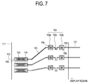
- a gate main line 121 of the display region is connected with a gate pad 124 through a fan-out part 123 of the non-display region.
- a gate signal is transmitted from a signal origination pad (e.g., IC connection pad, see 124 of FIG. 7 ) to gate electrode over a gate wire where the latter wire is formed on a first insulating substrate 111 .
- the gate wire may include a single or plural metal layers.
- the gate wire generally includes the gate main line 121 which is disposed in the display region and extends transversely, the gate electrode 122 which is connected with the gate main line 121 , the fan-out part 123 which extends from the gate main line 121 to the non-display region, and the gate pad 124 which is connected with an end part of the fan-out part 123 .
- a storage electrode line 125 often extends in parallel with the gate main line 121 as seen for example in FIG. 2 .
- the gate signal origination pad 124 is often connected with a packaging terminal or IC pin of a gate driver circuit (not shown) that outputs the gate signal to the pad end of the gate wire.
- the gate pad 124 has a substantially wider width than the gate main line 121 that connects that signal sourcing pad 124 to the gates of TFT's distributed along the gate main line 121 .
- a gate insulating layer 131 which in one embodiment is made of a silicon nitride (SiN x ) overlaps the gate electrode 122 and the gate wire 121 where the latter ( 121 , 122 ) are disposed on the first insulating substrate 111 .
- a semiconductor layer 132 which in one embodiment includes amorphous silicon (a-Si) is formed on the gate insulating layer 131 overlapping the gate electrode 122 .
- An ohmic contact layer 133 which in one embodiment includes n+hydrogenated amorphous silicon highly doped with an n-type dopant is formed on the semiconductor layer 132 .
- the ohmic contact layer 133 is selectively removed (etched away) from a channel between a source electrode 142 and a drain electrode 143 of the TFT (T).
- a data carrying wire is formed to extend over the drain's ohmic contact layer 133 and on top of the gate insulating layer 131 .
- the data wire may include a single or multiple layers of metal.
- the data wire includes a data line 141 which is shown extending vertically in FIG. 2 and crosses the gate main line 121 at a corner portion of the pixel area.
- the source electrode 142 branches out from the data line 141 and extends over the ohmic contact layer 133 .
- the drain electrode 143 which is separated from the source electrode 142 , extends over the ohmic contact layer 133 opposite to the source electrode 142 .
- a fan-out part 144 of the source line extends from the data main line 141 to the non-display region and a data drive pad 145 (belonging to a data driving circuit or IC, not shown) which is connected with an end of the fan-out part 144 .
- the data pad 145 is connected with a data driver circuit (not shown) and receives a data driving signal.
- the data pad 145 has a wider width than the data main line 141 .
- a passivation layer 151 is formed on the data wire and the semiconductor layer 132 that is not covered by the data wire.
- a contact hole 152 is formed on the passivation layer 151 to expose the drain electrode 143 therethrough.
- contact holes 153 , 154 and 155 are also formed on the passivation layer 151 .
- the gate insulating layer 131 is removed from the contact holes 153 , 154 and 155 .
- a pixel electrode 161 is formed on the passivation layer 151 .
- the pixel electrode 161 is typically made of a transparent conductive material such as indium tin oxide (ITO), indium zinc oxide (IZO), etc.
- the pixel electrode 161 is connected with the drain electrode 143 through the contact hole 152 .
- a pixel electrode splitting pattern 166 is defined (cut through) the pixel electrode 161 as shown.
- the pixel electrode cutting pattern 166 of the pixel electrode 161 divides the liquid crystal layer 300 into a plurality of regions, together with a common electrode cutting pattern 252 (to be described later).
- a black matrix 221 is formed on a second insulating substrate 211 .
- the black matrix 221 generally outlines a corresponding red, green or blue filter 231 and blocks light from being directly emitted through the area of the underlying thin film transistor (T) of the first substrate 100 .
- the black matrix 221 may include a photoresist organic material added with a black pigment.
- the black pigment may include carbon black or titanium oxide.
- a color filter 231 may include a bandpassing optical material such as one of red, green and blue filters that are repeatedly formed between areas of the black matrix 221 .
- the color filter 231 assigns color to light emitted from a backlight unit (not shown) and traveling through the liquid crystal layer 300 .
- the color filter 231 typically includes a photoresist organic material.
- An overcoat, planarizing layer 241 is typically formed on the color filter 231 and the black matrix 221 .
- the overcoat layer 241 provides planar surface even though the filter and matrix are of different thicknesses and the overcoat layer 241 protects the color filter 231 .
- the overcoat layer 241 may include a photoresist acrylic resin.
- a common electrode 251 is formed on the overcoat layer 241 .
- the common electrode 251 includes a transparent conductive material such as indium tin oxide (ITO), indium zinc oxide (IZO), etc.
- ITO indium tin oxide
- IZO indium zinc oxide
- the common electrode 251 supplies a voltage to one side of the liquid crystal material layer 300 , while the pixel electrode 161 of the thin film transistor substrate provides a second voltage to the other side so as to establish one or more electric filed patterns through the liquid crystal material layer 300 .
- the common electrode cutting pattern 252 is formed on the common electrode 251 .
- the common electrode cutting pattern 252 divides the liquid crystal layer 300 into a plurality of regions together with the pixel electrode cutting pattern 166 of the pixel electrode 161 .
- the pixel electrode cutting pattern 166 and the common electrode cutting pattern 252 are not limited to the V-shaped ones illustrated for the first embodiment, and may be, otherwise, formed in various shapes. In another embodiment of the present disclosure, a protrusion may be provided to divide the liquid crystal layer 300 into a plurality of regions instead of the cutting patterns 166 and 252 .
- the liquid crystal layer 300 is disposed between the first and second substrates 100 and 200 .
- the liquid crystal material layer 300 is a vertically aligned (VA) mode, in which a long axis of liquid crystal molecules is perpendicular to the first and second substrates 100 and 200 if not receiving a voltage.
- VA vertically aligned
- the liquid crystal molecules may lie irregularly in all directions since the lying direction is not determined by boundary conditions, thereby creating a disclination line on a boundary between different lying directions.
- the cutting patterns are organized 166 and 252 to form a fringe electric field when a voltage is supplied to the liquid crystal layer 300 and to thereby determine the lying direction of the liquid crystal molecules.
- the liquid crystal layer 300 is divided into plural regions by the cutting patterns 166 and 252 .
- the liquid crystal display device 1 has a normally black mode when no substantial voltage is applied across the liquid crystal material, and a transmissivity that is a function of the pixel voltage as is illustrated in the plot of FIG. 4 .
- the transmissivity variation in a low gradation shown in a part C in FIG. 4 is three times more drastic for the VA material than a twisted nematic liquid crystal.
- the gate main line 121 receives a gate signal through the gate pad 124 connected with the end part thereof. Due to a resistance of the gate main line 121 , the thin film transistor T adjacent to the gate pad 124 , i.e., a left thin film transistor T receives a short-delayed gate signal but the thin film transistor T far from the gate pad 123 , i.e., a right thin film transistor T receives a longer-delayed gate signal.
- the kick back voltage Vkb may be expressed by a formula 1 as follows.
- V kb ( V on ⁇ V off )* C p /( C lc +C st +C p ) Formula 1
- Cp refers to combined parasitic capacitance Cgs between the gate electrode and the source electrode and a parasitic capacitance Cgd between the gate electrode and the drain electrode
- Clc is a liquid crystal capacitance
- Cst is a storage capacitance
- Von is a gate on voltage
- Voff means a gate turn-off voltage.
- the gate-on voltage (Von) is not supplied in time, thereby decreasing the kick back voltage Vkb.
- the kick back voltage Vkb becomes larger when a negative pixel voltage is supplied rather than when a positive pixel voltage is supplied.
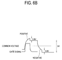
- FIGS. 6A and 6B respectively illustrate a kick back voltage Vkb of a pixel in a left-side display region having a short-delayed gate signal, and a pixel in a right-side display region having a longer-delayed gate signal.
- the kick back voltage is about 1.0V when the positive pixel voltage is supplied while it is about 1.2V when the negative pixel voltage is supplied.
- the kick back voltage is about 0.8V when both the positive pixel voltage and the negative pixel voltage are supplied.
- the left-side pixel has a larger root mean square pixel voltage that remains ultimately, and an image corresponding to the left-side pixel is seen as being comparatively brighter.
- the gate signal is shorter-delayed and the kick back voltage Vkb becomes larger if they are closer to the gate pad 124 . Conversely, the gate signal is longer-delayed and the kick back voltage Vkb becomes smaller if they are farther from the gate pad 124 .
- the left-side pixel has a larger root mean square pixel voltage than the right pixel to brighten the image corresponding to the left pixel more than that corresponding to the right pixel.
- the liquid crystal display device 1 according to the first embodiment of the present disclosure provides a compensating resistor 163 disposed between the gate main line 121 and the fan-out line 123 (and the gate pad 124 ) to reduce the above-mentioned problem.
- the resistor 163 is disposed between the fan-out part 123 and the gate main line 121 in the non-display region.
- the primary resistive material of resistor 163 is provided by the same layer that provides the primary material of the pixel electrode 161 .
- the resistor 163 includes a first part 163 a which is connected with the fan-out part 123 , a second part 163 b which is connected with the gate main line 121 and a third part 163 c which is electrically disposed between the first and second parts 163 a and 163 b.
- the first part 163 a contacts the fan-out part 123 through the contact hole 154 .
- the second part 163 b contacts the gate main line 121 through the contact hole 155 .
- the gate pad 124 exposed by the contact hole 153 is covered by a contact member 162 , where member 162 is comprised of the same material as that of the pixel electrode 161 and where member 162 is disposed in the same layer with the pixel electrode 161 .
- the resistor 163 can include one or more of optically transmissive electrical conductors such as indium tin oxide (ITO), indium zinc oxide (IZO), etc., which have a larger resistance than an optically opaque electrical conductor such as the metal material used in the gate main line 121 . Due to the resistor 163 having a substantially large resistance, the gate signal is substantially delayed before entering the display region, as shown in FIG. 9 and the difference in delay as shown by FIGS. 6A-6B is no longer a substantial factor in determining kick back.
- optically transmissive electrical conductors such as indium tin oxide (ITO), indium zinc oxide (IZO), etc.
- total resistance of the gate main line 121 is typically 4000 ⁇ to 7000 ⁇ while a total resistance of the resistor 163 may be 10% to 50% of the total resistance of the gate main line 121 .
- the resistance value of the resistor 163 may vary by changing one or more of a thickness, width and length attribute of the resistor 163 .
- the resistance value of the resistor 163 be set so that the gate signal delay variation due to resistance of the main gate line is substantially less than gate signal delay to total wire resistance.
- the gate signal delay value of a far right pixel of the display region is no more than about twice the gate signal delay value of the far left pixel in the display region (the one closest to the gate signal originating pad 124 .
- the distance between the gate main line 121 and the gate pad 124 is various, thereby causing a different resistance therebetween and irregular brightness.
- the length of the third part 163 c in the resistor 163 is in inverse proportion to the distance between the corresponding gate main line 121 and the gate pad 124 .
- brightness irregularity due to variation in distance between the gate main line 121 and the gate pad 124 decreases.
- the sealant 400 is disposed on the fan-out part 123 while the resistor 163 is provided inside the liquid crystal material containing area of the sealant 400 . Because the resistor 163 is not exposed to the outside, it is safe from being corroded.
- a flow of static electricity from the outside may damage the thin film transistor T.
- a substantial portion of the energy of the static electricity flow introduced from the gate pad 124 is dissipated in the resistor 163 having the larger resistance, thereby reducing problems due to static electricity.
- a resistor 163 according to another embodiment of the present disclosure may include other materials having a larger resistance than the gate main line 121 and being different from the material of the pixel electrode 161 .
- the shape of the resistor 163 is identical and the distance differences between the gate main line 121 and the gate pad 124 may be dealt with by changing the shape of the fan-out part 123 .
- FIG. 10 illustrates a brightness variation ratio depending on the gate signal delay value in the display region.
- BVR (Brightness of the left display region ⁇ Brightness of central display region)/(Brightness of central display region)*100.
- a large value means a large brightness difference.
- the brightness variation ratio (BVR) increases around 64% (from 30.6% to 50.3%).
- FIG. 11 illustrates a brightness variation ratio according to Cp/(Clc+Cst+Cp) in proportion to the kick back voltage. As shown therein, if Cp/(Clc+Cst+Cp) increases 24% (from 0.037 to 0.046), the brightness variation ratio rises approximately 26.4% (from 35.6% to 45%).
- brightness irregularity gets worse as variation in the gate signal delay value gets larger and/or as comparative contribution to kickback from the parasitic capacitance gets larger.
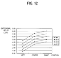
- the comparative amount of gate signal delay relative to position of the pixel electrode can be made to vary by changing a compensating or ballasting resistance in the non-display region, i.e., a resistance from the gate pad to the gate main line, which will be described with reference to the examples of FIGS. 12 and 13 .
- the resistance in the non-display region was switched over the following four values: 1 ⁇ 6 k ⁇ , 1 ⁇ 3 k ⁇ , 1 ⁇ 2 k ⁇ and 2 ⁇ 3 k ⁇ .
- the bottom most data plot having 0 k ⁇ is the case where there is no ballasting resistor and a gate main line and a gate pad are integrally formed in the same layer.
- the increased resistance of the ballasting resistor in the non-display region decreases the positionally-related differences in the gate signal delay and the positionally-related differences in the pixel voltage between the left-side display region and the right-side display region.
- the resistance of the ballasting resistor in the non-display region becomes larger, it also becomes more difficult to transmit a strong gate signal to each TFT.
- the resistance of the ballasting resistor should be determined as a compromise and in consideration of the total resistance of the gate main line 121 .
- FIG. 14 illustrates a part corresponding B area in FIG. 1 .
- an anti-static set of diode-connected MOSFETs 170 is formed on an outer circumference portion of each ballasting resistor 163 .
- the anti-static set 170 is electrically connected with a gate outer circumference and a common voltage line 146 . If static electricity is introduced through a gate pad 124 during a manufacturing process, the resistor 163 having a large resistance may be damaged, thereby causing disconnection. However, the anti-static set of diode-connected MOSFETs 170 is activated when the absolute value of voltage of the static exceed a predefined threshold and the activated set 170 scatters the introduced static electricity to the common voltage line (e.g., ground) 146 to prevent the resistor 163 from being damaged.
- the gate outer circumference portion refers a gate wire connected with the gate main line 121 and formed outside of the resistor 163 . That is, the gate outer circumference portion includes the gate pad 124 and the fan-out part 123 .
- the anti-static diode means 170 includes a plurality of thin film MOSFET transistors.
- the anti-static diode means 170 includes a first diode-connected MOSFET 171 and a second diode-connected MOSFET 172 coupled for carrying differently directed current flows.
- the first diode-connected MOSFET 171 is provided so that a negative going current flows from the gate outer circumference to the common voltage line 146 .
- the second diode-connected MOSFET 172 is provided so that a positive-going current flows from the common voltage line 146 to the gate outer circumference portion.
- the common voltage line 146 serves as an electrostatic bar with respect to the anti-static diode means 170 .
- a control terminal (gate) 1711 and an input terminal (drain) 1712 of the first diode-connected MOSFET 171 are connected with each other and with the gate line outer circumference ( 121 ).
- An output terminal (source) 1713 of the first diode-connected MOSFET 171 is connected with the common voltage line 146 .
- a bridge 1714 connects the input terminal (drain) 1712 to the gate outer circumference ( 121 ).
- MOSFET 171 If static electricity is inputted to the gate outer circumference and the static exceeds the predefined threshold (Vt) of MOSFET 171 , the control terminal 1711 connected with the gate outer circumference is switched to a turned on state, MOSFET 171 becomes conductive and thereby diverts the static electricity to the common voltage line 146 connected with the output terminal 1713 .
- Vt predefined threshold
- a control terminal (gate) 1721 and an input terminal (drain) 1722 of the second diode-connected MOSFET 172 are connected with the common voltage line 146 .
- An output terminal (source) 1723 of the second diode-connected MOSFET 172 is connected with the gate outer circumference ( 121 ).
- a second bridge 1724 connects the common voltage line 146 and the control terminal 1721 while a third bridge 1725 connects the output terminal 1723 and the gate outer circumference.
- MOSFET 172 If static electricity is inputted to the gate outer circumference and the static exceeds the predefined threshold (Vt) of MOSFET 172 , the control terminal 1721 connected with the gate outer circumference through the bridge 1724 is switched to a turned-on state, MOSFET 172 becomes conductive and thereby diverts the static electricity to the common voltage line 146 connected with the input terminal (drain) 1722 .
- Vt predefined threshold
- the anti-static diode means 170 may include only a first anti-static diode-connected MOSFET 171 without the second anti-static diode-connected MOSFET 172 .
- a gate pad 164 and a fan-out part 165 according to the third embodiment are integrally formed in a same layer with the ballasting resistor 163 .
- the gate pad 164 and the fan-out part 165 may include indium tin oxide (ITO) or indium zinc oxide (IZO).
- ITO indium tin oxide
- IZO indium zinc oxide
- the resistor 163 is connected with a gate main line 121 through a contact hole 156 .
- the gate pad 164 and the fan-out part 165 perform the same operation as the resistor 163 according to the first embodiment.
- the resistance of the ballasting resistor 163 is in inverse proportion to a distance between the corresponding gate main line 121 and the gate pad 164 as was the case for one version of the first embodiment.
- brightness irregularity due to a distance difference between the gate main line 121 and the gate pad 164 decreases.
- only a fan-out part 165 composed of a substantially resistive material such as indium tin oxide (ITO) or indium zinc oxide (IZO) may be provided to delay a corresponding gate signal, without forming a separate ballasting resistor 163 in the shape of the square waves such as shown in the lower two lines of FIG. 16 .
- ITO indium tin oxide
- IZO indium zinc oxide
- a liquid crystal display device according to a fourth embodiment will be described with reference to FIGS. 18 to 20 .
- a thin film transistor T is connected with two liquid crystal capacitances C LC1 and C LC2 .
- the first liquid crystal capacitance C LC1 is formed between a first pixel electrode PE 1 and a common electrode CE.
- the first pixel electrode PE 1 is directly connected with the thin film transistor T.
- the second liquid crystal capacitance C LC2 is formed between the second pixel electrode PE 2 and the common electrode CE.
- the second pixel electrode PE 2 is indirectly connected with the thin film transistor T through a coupling capacitance C CP .
- first pixel electrode PE 1 and the second pixel electrode PE 2 are electrically separated from each other due to the presence of coupling capacitance C CP and the second liquid crystal capacitance C LC2 .
- the liquid crystal display device according to the fourth embodiment can improve visibility per a mechanism which will be described with reference to FIG. 19 .
- the first pixel electrode PE 1 receives a data signal through the thin film transistor T.
- the second pixel electrode PE 2 receives a data signal by a voltage through a coupling capacitance C CP formed in an insulating layer between the second pixel electrode PE and the thin film transistor T, instead of directly receiving the data signal from the thin film transistor T.
- the second pixel electrode PE 2 receives a weaker signal than the first pixel electrode PE 1 , thereby causing a difference in brightness of the pixel region corresponding to the first pixel electrode PE 1 and the pixel region corresponding to the second pixel electrode PE 2 .
- the voltage supplied to the second pixel electrode PE 2 is 50% to 90% of the voltage supplied to the first pixel electrode PE 1 .
- a single pixel has a plurality of regions that have different gamma curves.
- the brightness and color in a front and lateral parts are compensated to improve lateral visibility.
- the pixel electrode 161 includes a first pixel electrode 161 a and a second pixel electrode 161 b which are separated from each other by a pixel electrode separating pattern 167 .
- the second pixel electrode 161 b has a trapezoid shape whose three sides are surrounded by the first pixel electrode 161 a .
- a pixel electrode cutting pattern 166 which is side by side with the pixel electrode separating pattern 167 is formed on the first and second pixel electrodes 161 a and 161 b.
- a drain electrode 143 includes a first drain electrode 143 a which is connected with the first pixel electrode 161 a and supplies an electrical signal thereto and a second drain electrode 143 b which extends below the second pixel electrode 161 b .
- the second drain electrode 143 b forms a coupling capacitance C CP together with the second pixel electrode 161 b.
- the pixel electrode separating pattern 167 and the pixel electrode cutting pattern 166 divide a liquid crystal layer 300 into a plurality of regions together with a common electrode cutting pattern 252 .
- a storage electrode line 125 is formed along the boundary of the pixel electrode 161 .
- Upper and lower storage electrode lines 125 are connected with each other through a contact hole 157 and a bridge electrode 168 .
- a liquid crystal display device according to a fifth embodiment of the present disclosure will be described with reference to FIG. 21 .
- a pixel electrode 161 has a rectangular shape as a whole.
- the pixel electrode 161 is elongated in an extension direction of a data line 141 .
- the pixel electrode 161 includes a first pixel electrode 161 a and a second pixel electrode 161 b which are separated from each other by a pixel electrode separating pattern 167 .
- the first pixel electrode 161 a is disposed in a center of a pixel and has a chevron-shape.
- the second pixel electrode 161 b surrounds an inside, an upper part and a lower part of the first pixel electrode 161 a .
- the second pixel electrode 161 b is larger than the first pixel electrode 161 a.
- a thin film transistor T includes a first thin film transistor TFT 1 which is connected with the first pixel electrode 161 a and a second thin film transistor TFT 2 which is connected with the second pixel electrode 161 b.
- a drain electrode 143 of the respective thin film transistors TFT 1 and TFT 2 overlaps the pixel electrode 161 to form a storage capacitance Cst.
- the storage capacitance Cst is proportional to an overlapping size of the drain electrode 143 and the pixel electrode 161 .
- respective pixel electrodes 161 a and 161 b receive different pixel voltages by using independent thin film transistors TFT 1 and TFT 2 .
- the method of improving visibility in the fifth embodiment is the same as that in the fourth embodiment. Thus the detailed description will not be provided here.
- the configuration of the non-display region in the fourth and fifth embodiments can be the same as that in the first to third embodiment of the present disclosure.
- the liquid crystal capacitance Clc and the storage capacitance Cst are small.
- the kick back voltage Vkb becomes larger, thereby making the brightness difference (refer to Formula 1) more significant.
- the present disclosure of invention provides a liquid crystal display device which reduces a brightness irregularity due to a gate signal delay difference.
Landscapes
- Physics & Mathematics (AREA)
- Nonlinear Science (AREA)
- Engineering & Computer Science (AREA)
- Crystallography & Structural Chemistry (AREA)
- General Physics & Mathematics (AREA)
- Chemical & Material Sciences (AREA)
- Optics & Photonics (AREA)
- Microelectronics & Electronic Packaging (AREA)
- Mathematical Physics (AREA)
- Computer Hardware Design (AREA)
- Theoretical Computer Science (AREA)
- Liquid Crystal (AREA)
- Devices For Indicating Variable Information By Combining Individual Elements (AREA)
Applications Claiming Priority (6)
| Application Number | Priority Date | Filing Date | Title |
|---|---|---|---|
| KR10-2006-0081056 | 2006-08-25 | ||
| KR20060081056 | 2006-08-25 | ||
| KR1020060124754A KR101392160B1 (ko) | 2006-08-25 | 2006-12-08 | 액정표시장치 |
| KR10-2006-0124754 | 2006-12-08 | ||
| KR10-2007-0015821 | 2007-02-15 | ||
| KR1020070015821A KR20080076196A (ko) | 2007-02-15 | 2007-02-15 | 액정표시장치 |
Publications (2)
| Publication Number | Publication Date |
|---|---|
| US20080049156A1 US20080049156A1 (en) | 2008-02-28 |
| US8089598B2 true US8089598B2 (en) | 2012-01-03 |
Family
ID=38669798
Family Applications (1)
| Application Number | Title | Priority Date | Filing Date |
|---|---|---|---|
| US11/843,980 Active 2029-04-13 US8089598B2 (en) | 2006-08-25 | 2007-08-23 | Liquid crystal display device having delay compensation |
Country Status (3)
| Country | Link |
|---|---|
| US (1) | US8089598B2 (ja) |
| EP (1) | EP1892697B1 (ja) |
| JP (1) | JP5727120B2 (ja) |
Cited By (7)
| Publication number | Priority date | Publication date | Assignee | Title |
|---|---|---|---|---|
| US20100296015A1 (en) * | 2009-05-19 | 2010-11-25 | Samsung Electronics Co., Ltd. | Liquid crystal display |
| US20140159204A1 (en) * | 2012-12-11 | 2014-06-12 | Beijing Boe Display Technology Co., Ltd. | Array substrate, fabrication method thereof and display device |
| US20140301001A1 (en) * | 2013-04-04 | 2014-10-09 | Samsung Electronics Co., Ltd. | Source Driving Integrated Circuits Including an Electrostatic Discharge Circuit and Related Layout Method |
| US20160148549A1 (en) * | 2014-11-26 | 2016-05-26 | Mitsubishi Electric Corporation | Liquid crystal display apparatus |
| US20160284298A1 (en) * | 2015-03-25 | 2016-09-29 | JVC Kenwood Corporation | Liquid crystal display device |
| US9678371B2 (en) | 2015-06-01 | 2017-06-13 | Apple Inc. | Display with delay compensation to prevent block dimming |
| US11024246B2 (en) * | 2018-11-09 | 2021-06-01 | Sakai Display Products Corporation | Display apparatus and method for driving display panel with scanning line clock signal or scanning line signal correcting unit |
Families Citing this family (29)
| Publication number | Priority date | Publication date | Assignee | Title |
|---|---|---|---|---|
| JP5131525B2 (ja) * | 2007-11-16 | 2013-01-30 | Nltテクノロジー株式会社 | アクティブマトリクス型液晶表示装置 |
| KR101574127B1 (ko) * | 2008-09-29 | 2015-12-04 | 삼성디스플레이 주식회사 | 액정 표시 장치 |
| KR101490485B1 (ko) * | 2008-10-30 | 2015-02-05 | 삼성디스플레이 주식회사 | 액정 표시 장치 및 그 제조 방법 |
| KR102020739B1 (ko) * | 2009-12-18 | 2019-09-10 | 가부시키가이샤 한도오따이 에네루기 켄큐쇼 | 광 센서를 포함하는 표시 장치 및 그 구동 방법 |
| JP5736895B2 (ja) * | 2011-03-28 | 2015-06-17 | 三菱電機株式会社 | 横電界方式の液晶表示装置 |
| TWI454811B (zh) * | 2011-05-20 | 2014-10-01 | Innolux Display Corp | 顯示面板 |
| JP5901007B2 (ja) * | 2011-09-12 | 2016-04-06 | 株式会社ジャパンディスプレイ | 表示装置 |
| KR102043624B1 (ko) * | 2012-12-17 | 2019-11-12 | 엘지디스플레이 주식회사 | 액정표시장치 및 그 구동방법 |
| US9835856B2 (en) * | 2013-05-24 | 2017-12-05 | Raytheon Company | Adaptive optic having meander resistors |
| JP6207341B2 (ja) * | 2013-10-24 | 2017-10-04 | 株式会社ジャパンディスプレイ | 表示装置 |
| CN103838049B (zh) * | 2014-03-10 | 2017-02-22 | 深圳市华星光电技术有限公司 | 阵列基板及液晶显示面板 |
| KR102219516B1 (ko) * | 2014-04-10 | 2021-02-25 | 삼성디스플레이 주식회사 | 표시 기판 |
| CN103956132B (zh) * | 2014-04-23 | 2017-02-15 | 京东方科技集团股份有限公司 | 驱动电路、显示装置及实现多条传输线路等电阻的方法 |
| CN104166284B (zh) * | 2014-08-27 | 2018-01-09 | 深圳市华星光电技术有限公司 | 液晶显示面板及其扇形区域 |
| KR102238639B1 (ko) * | 2014-10-14 | 2021-04-12 | 엘지디스플레이 주식회사 | 게이트신호의 딜레이 편차를 경감할 수 있는 액정표시장치 |
| KR102196101B1 (ko) * | 2014-10-23 | 2020-12-30 | 삼성디스플레이 주식회사 | 표시 장치 |
| TWI504969B (zh) * | 2014-10-27 | 2015-10-21 | Au Optronics Corp | 顯示面板以及顯示裝置 |
| CN104391411B (zh) * | 2014-12-16 | 2017-06-06 | 深圳市华星光电技术有限公司 | 一种液晶显示面板 |
| JPWO2016152492A1 (ja) * | 2015-03-26 | 2017-12-28 | 富士フイルム株式会社 | マトリクス装置およびマトリクス装置の製造方法 |
| CN105047156B (zh) * | 2015-08-18 | 2017-08-04 | 青岛海信电器股份有限公司 | 液晶面板驱动方法、装置与液晶显示器 |
| CN107561799B (zh) * | 2017-08-25 | 2021-07-20 | 厦门天马微电子有限公司 | 一种阵列基板、显示面板及显示装置 |
| CN107611142B (zh) * | 2017-09-11 | 2020-06-09 | 上海天马有机发光显示技术有限公司 | 显示面板及显示装置 |
| CN107634072B (zh) * | 2017-10-25 | 2020-04-03 | 厦门天马微电子有限公司 | 阵列基板及显示面板 |
| CN107610636B (zh) * | 2017-10-30 | 2021-02-02 | 武汉天马微电子有限公司 | 一种显示面板及显示装置 |
| CN108598088B (zh) * | 2018-04-27 | 2019-10-11 | 武汉华星光电技术有限公司 | Tft阵列基板及显示装置 |
| JP7181824B2 (ja) * | 2019-03-22 | 2022-12-01 | 株式会社ジャパンディスプレイ | 表示装置 |
| CN110322856A (zh) * | 2019-07-18 | 2019-10-11 | 深圳市华星光电半导体显示技术有限公司 | 一种液晶显示面板及其驱动方法 |
| CN110853511B (zh) * | 2019-10-24 | 2021-07-06 | Tcl华星光电技术有限公司 | 一种阵列基板 |
| CN111445831B (zh) * | 2020-04-24 | 2021-08-03 | 深圳市华星光电半导体显示技术有限公司 | 一种显示面板 |
Citations (22)
| Publication number | Priority date | Publication date | Assignee | Title |
|---|---|---|---|---|
| JPS63198022A (ja) | 1987-02-13 | 1988-08-16 | Fujitsu Ltd | アクテイブマトリクス型液晶表示装置 |
| JPH04313733A (ja) | 1991-03-22 | 1992-11-05 | Mitsubishi Electric Corp | マトリックス型表示装置 |
| JPH07218896A (ja) | 1994-02-02 | 1995-08-18 | Sanyo Electric Co Ltd | アクティブマトリックス型液晶表示装置 |
| US5598178A (en) * | 1993-12-22 | 1997-01-28 | Sharp Kabushiki Kaisha | Liquid crystal display |
| US6072550A (en) * | 1996-06-11 | 2000-06-06 | Samsung Electronics Co., Ltd. | Liquid crystal display having resistive electrostatic discharge protection devices with resistance no greater than 1 MOHM and method of fabrication |
| US6104465A (en) * | 1995-12-30 | 2000-08-15 | Samsung Electronics Co., Ltd. | Liquid crystal display panels having control lines with uniforms resistance |
| US20030227078A1 (en) * | 2002-06-07 | 2003-12-11 | Samsung Electronics Co., Ltd. | Thin film transistor array panel for a liquid crystal display |
| JP2004125895A (ja) * | 2002-09-30 | 2004-04-22 | Victor Co Of Japan Ltd | アクティブマトリクス型表示装置 |
| US20040114059A1 (en) | 2001-09-26 | 2004-06-17 | Lee Chang-Hun | Thin film transistor array panel for liquid crystal display and method for manufacturing the same |
| US20040135956A1 (en) | 2002-08-07 | 2004-07-15 | Samsung Electronics Co., Ltd. | Integrated circuit and display device including integrated circuit |
| US20050018121A1 (en) | 2003-07-23 | 2005-01-27 | Tean-Sen Jen | Liquid crystal display panel with reduced flicker |
| US20050179631A1 (en) | 2003-12-30 | 2005-08-18 | Samsung Electronics Co., Ltd. | Liquid crystal display |
| US20060001640A1 (en) * | 1998-09-19 | 2006-01-05 | Hyun Chang Lee | Active matrix liquid crystal display |
| US20060066792A1 (en) * | 2002-12-13 | 2006-03-30 | Sung-Hun Oh | Liquid crystal display device having variable viewing angle |
| US20060114209A1 (en) | 2004-11-26 | 2006-06-01 | Samsung Electronics Co., Ltd. | Gate line driving circuit, display device having the same, and apparatus and method for driving the display device |
| EP1674922A1 (en) | 2004-12-27 | 2006-06-28 | Samsung Electronics Co., Ltd. | Liquid crystal display |
| US20060186913A1 (en) * | 2005-02-22 | 2006-08-24 | Dong-Gyu Kim | Liquid crystal display and test method thereof |
| US20060208658A1 (en) * | 2005-03-18 | 2006-09-21 | Lg Electronics Inc. | Light emitting device |
| US20060286703A1 (en) * | 2005-05-25 | 2006-12-21 | Yoon-Sung Um | Thin film transistor array panel and liquid crystal display including the same |
| US20070080433A1 (en) * | 2005-10-06 | 2007-04-12 | Au Optronics Corp. | Display panels |
| US7206057B2 (en) * | 2003-11-10 | 2007-04-17 | Lg.Philips Lcd Co., Ltd. | Liquid crystal display panel and fabricating method thereof |
| US20070085963A1 (en) * | 2005-10-18 | 2007-04-19 | Au Optronics Corporation | Electrical connectors between electronic devices |
Family Cites Families (8)
| Publication number | Priority date | Publication date | Assignee | Title |
|---|---|---|---|---|
| JP2846351B2 (ja) * | 1989-07-27 | 1999-01-13 | 株式会社日立製作所 | 液晶表示装置 |
| JPH07253596A (ja) * | 1994-03-16 | 1995-10-03 | Fujitsu Ltd | 表示装置 |
| JPH08179360A (ja) * | 1994-12-20 | 1996-07-12 | Casio Comput Co Ltd | アクティブマトリックスパネル |
| JPH11218782A (ja) * | 1998-02-03 | 1999-08-10 | Casio Comput Co Ltd | アクティブマトリックス型液晶表示装置 |
| JP4777500B2 (ja) * | 2000-06-19 | 2011-09-21 | 三菱電機株式会社 | アレイ基板およびそれを用いた表示装置ならびにアレイ基板の製造方法 |
| US6842200B1 (en) * | 2003-06-18 | 2005-01-11 | Hannstar Display Corporation | Liquid crystal panel having compensation capacitors for balancing RC delay effect |
| TWI236184B (en) * | 2004-05-06 | 2005-07-11 | Quanta Display Inc | Wiring structure and flat panel display |
| JP5143362B2 (ja) * | 2005-02-07 | 2013-02-13 | 三星電子株式会社 | 液晶表示装置 |
-
2007
- 2007-07-06 JP JP2007179002A patent/JP5727120B2/ja active Active
- 2007-08-23 US US11/843,980 patent/US8089598B2/en active Active
- 2007-08-24 EP EP07016646A patent/EP1892697B1/en active Active
Patent Citations (23)
| Publication number | Priority date | Publication date | Assignee | Title |
|---|---|---|---|---|
| JPS63198022A (ja) | 1987-02-13 | 1988-08-16 | Fujitsu Ltd | アクテイブマトリクス型液晶表示装置 |
| JPH04313733A (ja) | 1991-03-22 | 1992-11-05 | Mitsubishi Electric Corp | マトリックス型表示装置 |
| US5598178A (en) * | 1993-12-22 | 1997-01-28 | Sharp Kabushiki Kaisha | Liquid crystal display |
| JPH07218896A (ja) | 1994-02-02 | 1995-08-18 | Sanyo Electric Co Ltd | アクティブマトリックス型液晶表示装置 |
| US6104465A (en) * | 1995-12-30 | 2000-08-15 | Samsung Electronics Co., Ltd. | Liquid crystal display panels having control lines with uniforms resistance |
| US6072550A (en) * | 1996-06-11 | 2000-06-06 | Samsung Electronics Co., Ltd. | Liquid crystal display having resistive electrostatic discharge protection devices with resistance no greater than 1 MOHM and method of fabrication |
| US20060001640A1 (en) * | 1998-09-19 | 2006-01-05 | Hyun Chang Lee | Active matrix liquid crystal display |
| US7209192B2 (en) * | 2001-09-26 | 2007-04-24 | Samsung Electronics Co., Ltd. | Thin film transistor array panel for liquid crystal display and method for manufacturing the same |
| US20040114059A1 (en) | 2001-09-26 | 2004-06-17 | Lee Chang-Hun | Thin film transistor array panel for liquid crystal display and method for manufacturing the same |
| US20030227078A1 (en) * | 2002-06-07 | 2003-12-11 | Samsung Electronics Co., Ltd. | Thin film transistor array panel for a liquid crystal display |
| US20040135956A1 (en) | 2002-08-07 | 2004-07-15 | Samsung Electronics Co., Ltd. | Integrated circuit and display device including integrated circuit |
| JP2004125895A (ja) * | 2002-09-30 | 2004-04-22 | Victor Co Of Japan Ltd | アクティブマトリクス型表示装置 |
| US20060066792A1 (en) * | 2002-12-13 | 2006-03-30 | Sung-Hun Oh | Liquid crystal display device having variable viewing angle |
| US20050018121A1 (en) | 2003-07-23 | 2005-01-27 | Tean-Sen Jen | Liquid crystal display panel with reduced flicker |
| US7206057B2 (en) * | 2003-11-10 | 2007-04-17 | Lg.Philips Lcd Co., Ltd. | Liquid crystal display panel and fabricating method thereof |
| US20050179631A1 (en) | 2003-12-30 | 2005-08-18 | Samsung Electronics Co., Ltd. | Liquid crystal display |
| US20060114209A1 (en) | 2004-11-26 | 2006-06-01 | Samsung Electronics Co., Ltd. | Gate line driving circuit, display device having the same, and apparatus and method for driving the display device |
| EP1674922A1 (en) | 2004-12-27 | 2006-06-28 | Samsung Electronics Co., Ltd. | Liquid crystal display |
| US20060186913A1 (en) * | 2005-02-22 | 2006-08-24 | Dong-Gyu Kim | Liquid crystal display and test method thereof |
| US20060208658A1 (en) * | 2005-03-18 | 2006-09-21 | Lg Electronics Inc. | Light emitting device |
| US20060286703A1 (en) * | 2005-05-25 | 2006-12-21 | Yoon-Sung Um | Thin film transistor array panel and liquid crystal display including the same |
| US20070080433A1 (en) * | 2005-10-06 | 2007-04-12 | Au Optronics Corp. | Display panels |
| US20070085963A1 (en) * | 2005-10-18 | 2007-04-19 | Au Optronics Corporation | Electrical connectors between electronic devices |
Non-Patent Citations (2)
| Title |
|---|
| European Application No. EP0716646.7, Examination Report, Apr. 26, 2010, 9 pp. |
| European Application No. EP0716646.7, Search Report, Apr. 26, 2010, 12 pp. |
Cited By (14)
| Publication number | Priority date | Publication date | Assignee | Title |
|---|---|---|---|---|
| US8427594B2 (en) * | 2009-05-19 | 2013-04-23 | Samsung Display Co., Ltd. | Liquid crystal display |
| US20130215344A1 (en) * | 2009-05-19 | 2013-08-22 | Samsung Display Co., Ltd. | Liquid crystal display |
| US8964140B2 (en) * | 2009-05-19 | 2015-02-24 | Samsung Display Co., Ltd. | Liquid crystal display |
| US20100296015A1 (en) * | 2009-05-19 | 2010-11-25 | Samsung Electronics Co., Ltd. | Liquid crystal display |
| US9673225B2 (en) * | 2012-12-11 | 2017-06-06 | Boe Technology Group Co., Ltd. | Array substrate, fabrication method thereof and display device |
| US20140159204A1 (en) * | 2012-12-11 | 2014-06-12 | Beijing Boe Display Technology Co., Ltd. | Array substrate, fabrication method thereof and display device |
| US20140301001A1 (en) * | 2013-04-04 | 2014-10-09 | Samsung Electronics Co., Ltd. | Source Driving Integrated Circuits Including an Electrostatic Discharge Circuit and Related Layout Method |
| US9735053B2 (en) * | 2013-04-04 | 2017-08-15 | Samsung Electronics Co., Ltd. | Source driving integrated circuits including an electrostatic discharge circuit and related layout method |
| US20160148549A1 (en) * | 2014-11-26 | 2016-05-26 | Mitsubishi Electric Corporation | Liquid crystal display apparatus |
| US9875675B2 (en) * | 2014-11-26 | 2018-01-23 | Mitsubishi Electric Corporation | Liquid crystal display apparatus |
| US20160284298A1 (en) * | 2015-03-25 | 2016-09-29 | JVC Kenwood Corporation | Liquid crystal display device |
| US9824654B2 (en) * | 2015-03-25 | 2017-11-21 | JVC Kenwood Corporation | Liquid crystal display device |
| US9678371B2 (en) | 2015-06-01 | 2017-06-13 | Apple Inc. | Display with delay compensation to prevent block dimming |
| US11024246B2 (en) * | 2018-11-09 | 2021-06-01 | Sakai Display Products Corporation | Display apparatus and method for driving display panel with scanning line clock signal or scanning line signal correcting unit |
Also Published As
| Publication number | Publication date |
|---|---|
| EP1892697B1 (en) | 2012-10-10 |
| EP1892697A1 (en) | 2008-02-27 |
| JP5727120B2 (ja) | 2015-06-03 |
| JP2008052258A (ja) | 2008-03-06 |
| US20080049156A1 (en) | 2008-02-28 |
Similar Documents
| Publication | Publication Date | Title |
|---|---|---|
| US8089598B2 (en) | Liquid crystal display device having delay compensation | |
| US10453869B2 (en) | Display apparatus | |
| KR101392160B1 (ko) | 액정표시장치 | |
| US9341907B2 (en) | Liquid crystal display | |
| KR101319347B1 (ko) | 터치 패널 일체형 액정 표시 장치 | |
| KR101439268B1 (ko) | 횡전계 방식 액정표시장치용 어레이 기판 | |
| US7952674B2 (en) | Display device having counter-twisting liquid crystal areas and method of operating and manufacturing the same | |
| US7626649B2 (en) | Liquid crystal display device | |
| US20180067357A1 (en) | Display device | |
| KR102329979B1 (ko) | 액정표시장치 | |
| KR101310309B1 (ko) | 표시패널 | |
| KR102367963B1 (ko) | 액정 표시 장치 | |
| US11366540B2 (en) | Display device | |
| JP5429776B2 (ja) | 液晶表示パネル | |
| KR20060114921A (ko) | 액정 표시 장치 | |
| TW201633092A (zh) | 位置輸入裝置及具有位置輸入功能之顯示裝置 | |
| KR20130042242A (ko) | 액정 표시 장치 | |
| KR20080022355A (ko) | 액정표시장치 | |
| KR20160142443A (ko) | 액정 표시 장치 | |
| KR20060062908A (ko) | 액정 표시 패널 | |
| KR20080076196A (ko) | 액정표시장치 | |
| US20240105735A1 (en) | Array substrate and display device | |
| KR101471144B1 (ko) | 스토리지 전압의 검출 방법, 검출된 스토리지 전압을이용하는 표시 장치 및 이의 구동 방법 | |
| KR20080011598A (ko) | 액정표시장치와 이의 제조방법 | |
| KR20080030877A (ko) | 액정표시장치 |
Legal Events
| Date | Code | Title | Description |
|---|---|---|---|
| AS | Assignment |
Owner name: SAMSUNG ELECTRONICS CO., LTD., KOREA, REPUBLIC OF Free format text: ASSIGNMENT OF ASSIGNORS INTEREST;ASSIGNORS:KIM, DONG-GYU;NA, BYOUNG-SUN;REEL/FRAME:019738/0430 Effective date: 20070822 |
|
| FEPP | Fee payment procedure |
Free format text: PAYOR NUMBER ASSIGNED (ORIGINAL EVENT CODE: ASPN); ENTITY STATUS OF PATENT OWNER: LARGE ENTITY |
|
| STCF | Information on status: patent grant |
Free format text: PATENTED CASE |
|
| AS | Assignment |
Owner name: SAMSUNG DISPLAY CO., LTD., KOREA, REPUBLIC OF Free format text: ASSIGNMENT OF ASSIGNORS INTEREST;ASSIGNOR:SAMSUNG ELECTRONICS CO., LTD.;REEL/FRAME:028991/0677 Effective date: 20120904 |
|
| FPAY | Fee payment |
Year of fee payment: 4 |
|
| MAFP | Maintenance fee payment |
Free format text: PAYMENT OF MAINTENANCE FEE, 8TH YEAR, LARGE ENTITY (ORIGINAL EVENT CODE: M1552); ENTITY STATUS OF PATENT OWNER: LARGE ENTITY Year of fee payment: 8 |
|
| MAFP | Maintenance fee payment |
Free format text: PAYMENT OF MAINTENANCE FEE, 12TH YEAR, LARGE ENTITY (ORIGINAL EVENT CODE: M1553); ENTITY STATUS OF PATENT OWNER: LARGE ENTITY Year of fee payment: 12 |