EP1892697B1 - Liquid crystal display device having delay compensation - Google Patents
Liquid crystal display device having delay compensation Download PDFInfo
- Publication number
- EP1892697B1 EP1892697B1 EP07016646A EP07016646A EP1892697B1 EP 1892697 B1 EP1892697 B1 EP 1892697B1 EP 07016646 A EP07016646 A EP 07016646A EP 07016646 A EP07016646 A EP 07016646A EP 1892697 B1 EP1892697 B1 EP 1892697B1
- Authority
- EP
- European Patent Office
- Prior art keywords
- gate
- liquid crystal
- display device
- crystal display
- pixel electrode
- Prior art date
- Legal status (The legal status is an assumption and is not a legal conclusion. Google has not performed a legal analysis and makes no representation as to the accuracy of the status listed.)
- Active
Links
- 239000004973 liquid crystal related substance Substances 0.000 title claims description 73
- 239000000758 substrate Substances 0.000 claims description 39
- 239000010409 thin film Substances 0.000 claims description 29
- 239000000463 material Substances 0.000 claims description 18
- 238000003860 storage Methods 0.000 claims description 9
- 239000000565 sealant Substances 0.000 claims description 7
- 239000004020 conductor Substances 0.000 claims description 6
- 230000008878 coupling Effects 0.000 claims description 6
- 238000010168 coupling process Methods 0.000 claims description 6
- 238000005859 coupling reaction Methods 0.000 claims description 6
- AMGQUBHHOARCQH-UHFFFAOYSA-N indium;oxotin Chemical compound [In].[Sn]=O AMGQUBHHOARCQH-UHFFFAOYSA-N 0.000 claims description 6
- YVTHLONGBIQYBO-UHFFFAOYSA-N zinc indium(3+) oxygen(2-) Chemical compound [O--].[Zn++].[In+3] YVTHLONGBIQYBO-UHFFFAOYSA-N 0.000 claims description 6
- 239000010410 layer Substances 0.000 description 45
- 238000005520 cutting process Methods 0.000 description 14
- 230000003068 static effect Effects 0.000 description 12
- 230000005611 electricity Effects 0.000 description 9
- 230000007423 decrease Effects 0.000 description 8
- 239000011159 matrix material Substances 0.000 description 6
- 230000003071 parasitic effect Effects 0.000 description 6
- 230000003111 delayed effect Effects 0.000 description 5
- 239000010408 film Substances 0.000 description 4
- 238000002161 passivation Methods 0.000 description 4
- 101100489584 Solanum lycopersicum TFT1 gene Proteins 0.000 description 3
- 101100214488 Solanum lycopersicum TFT2 gene Proteins 0.000 description 3
- 229910021417 amorphous silicon Inorganic materials 0.000 description 3
- 230000001186 cumulative effect Effects 0.000 description 3
- 230000000694 effects Effects 0.000 description 3
- 230000005684 electric field Effects 0.000 description 3
- 229920002120 photoresistant polymer Polymers 0.000 description 3
- 239000004065 semiconductor Substances 0.000 description 3
- 230000005540 biological transmission Effects 0.000 description 2
- 230000008859 change Effects 0.000 description 2
- 230000000052 comparative effect Effects 0.000 description 2
- 239000013256 coordination polymer Substances 0.000 description 2
- 230000001788 irregular Effects 0.000 description 2
- 238000004519 manufacturing process Methods 0.000 description 2
- 229910052751 metal Inorganic materials 0.000 description 2
- 239000002184 metal Substances 0.000 description 2
- 230000003287 optical effect Effects 0.000 description 2
- 239000011368 organic material Substances 0.000 description 2
- 239000000049 pigment Substances 0.000 description 2
- 230000008054 signal transmission Effects 0.000 description 2
- 239000004925 Acrylic resin Substances 0.000 description 1
- 229920000178 Acrylic resin Polymers 0.000 description 1
- 239000004988 Nematic liquid crystal Substances 0.000 description 1
- 229910052581 Si3N4 Inorganic materials 0.000 description 1
- 229910004205 SiNX Inorganic materials 0.000 description 1
- GWEVSGVZZGPLCZ-UHFFFAOYSA-N Titan oxide Chemical compound O=[Ti]=O GWEVSGVZZGPLCZ-UHFFFAOYSA-N 0.000 description 1
- 239000006229 carbon black Substances 0.000 description 1
- 230000015556 catabolic process Effects 0.000 description 1
- 230000003247 decreasing effect Effects 0.000 description 1
- 238000006731 degradation reaction Methods 0.000 description 1
- 230000001419 dependent effect Effects 0.000 description 1
- 238000010586 diagram Methods 0.000 description 1
- 238000009826 distribution Methods 0.000 description 1
- 239000002019 doping agent Substances 0.000 description 1
- 230000006872 improvement Effects 0.000 description 1
- 230000007246 mechanism Effects 0.000 description 1
- 239000007769 metal material Substances 0.000 description 1
- 238000000034 method Methods 0.000 description 1
- 238000004806 packaging method and process Methods 0.000 description 1
- 230000003252 repetitive effect Effects 0.000 description 1
- 230000000630 rising effect Effects 0.000 description 1
- HQVNEWCFYHHQES-UHFFFAOYSA-N silicon nitride Chemical compound N12[Si]34N5[Si]62N3[Si]51N64 HQVNEWCFYHHQES-UHFFFAOYSA-N 0.000 description 1
- 239000002356 single layer Substances 0.000 description 1
- 238000012358 sourcing Methods 0.000 description 1
- OGIDPMRJRNCKJF-UHFFFAOYSA-N titanium oxide Inorganic materials [Ti]=O OGIDPMRJRNCKJF-UHFFFAOYSA-N 0.000 description 1
Images


Classifications
-
- G—PHYSICS
- G02—OPTICS
- G02F—OPTICAL DEVICES OR ARRANGEMENTS FOR THE CONTROL OF LIGHT BY MODIFICATION OF THE OPTICAL PROPERTIES OF THE MEDIA OF THE ELEMENTS INVOLVED THEREIN; NON-LINEAR OPTICS; FREQUENCY-CHANGING OF LIGHT; OPTICAL LOGIC ELEMENTS; OPTICAL ANALOGUE/DIGITAL CONVERTERS
- G02F1/00—Devices or arrangements for the control of the intensity, colour, phase, polarisation or direction of light arriving from an independent light source, e.g. switching, gating or modulating; Non-linear optics
- G02F1/01—Devices or arrangements for the control of the intensity, colour, phase, polarisation or direction of light arriving from an independent light source, e.g. switching, gating or modulating; Non-linear optics for the control of the intensity, phase, polarisation or colour
- G02F1/13—Devices or arrangements for the control of the intensity, colour, phase, polarisation or direction of light arriving from an independent light source, e.g. switching, gating or modulating; Non-linear optics for the control of the intensity, phase, polarisation or colour based on liquid crystals, e.g. single liquid crystal display cells
- G02F1/133—Constructional arrangements; Operation of liquid crystal cells; Circuit arrangements
- G02F1/136—Liquid crystal cells structurally associated with a semi-conducting layer or substrate, e.g. cells forming part of an integrated circuit
- G02F1/1362—Active matrix addressed cells
- G02F1/136286—Wiring, e.g. gate line, drain line
-
- G—PHYSICS
- G02—OPTICS
- G02F—OPTICAL DEVICES OR ARRANGEMENTS FOR THE CONTROL OF LIGHT BY MODIFICATION OF THE OPTICAL PROPERTIES OF THE MEDIA OF THE ELEMENTS INVOLVED THEREIN; NON-LINEAR OPTICS; FREQUENCY-CHANGING OF LIGHT; OPTICAL LOGIC ELEMENTS; OPTICAL ANALOGUE/DIGITAL CONVERTERS
- G02F1/00—Devices or arrangements for the control of the intensity, colour, phase, polarisation or direction of light arriving from an independent light source, e.g. switching, gating or modulating; Non-linear optics
- G02F1/01—Devices or arrangements for the control of the intensity, colour, phase, polarisation or direction of light arriving from an independent light source, e.g. switching, gating or modulating; Non-linear optics for the control of the intensity, phase, polarisation or colour
- G02F1/13—Devices or arrangements for the control of the intensity, colour, phase, polarisation or direction of light arriving from an independent light source, e.g. switching, gating or modulating; Non-linear optics for the control of the intensity, phase, polarisation or colour based on liquid crystals, e.g. single liquid crystal display cells
- G02F1/137—Devices or arrangements for the control of the intensity, colour, phase, polarisation or direction of light arriving from an independent light source, e.g. switching, gating or modulating; Non-linear optics for the control of the intensity, phase, polarisation or colour based on liquid crystals, e.g. single liquid crystal display cells characterised by the electro-optical or magneto-optical effect, e.g. field-induced phase transition, orientation effect, guest-host interaction or dynamic scattering
- G02F1/139—Devices or arrangements for the control of the intensity, colour, phase, polarisation or direction of light arriving from an independent light source, e.g. switching, gating or modulating; Non-linear optics for the control of the intensity, phase, polarisation or colour based on liquid crystals, e.g. single liquid crystal display cells characterised by the electro-optical or magneto-optical effect, e.g. field-induced phase transition, orientation effect, guest-host interaction or dynamic scattering based on orientation effects in which the liquid crystal remains transparent
- G02F1/1393—Devices or arrangements for the control of the intensity, colour, phase, polarisation or direction of light arriving from an independent light source, e.g. switching, gating or modulating; Non-linear optics for the control of the intensity, phase, polarisation or colour based on liquid crystals, e.g. single liquid crystal display cells characterised by the electro-optical or magneto-optical effect, e.g. field-induced phase transition, orientation effect, guest-host interaction or dynamic scattering based on orientation effects in which the liquid crystal remains transparent the birefringence of the liquid crystal being electrically controlled, e.g. ECB-, DAP-, HAN-, PI-LC cells
-
- G—PHYSICS
- G09—EDUCATION; CRYPTOGRAPHY; DISPLAY; ADVERTISING; SEALS
- G09G—ARRANGEMENTS OR CIRCUITS FOR CONTROL OF INDICATING DEVICES USING STATIC MEANS TO PRESENT VARIABLE INFORMATION
- G09G3/00—Control arrangements or circuits, of interest only in connection with visual indicators other than cathode-ray tubes
- G09G3/20—Control arrangements or circuits, of interest only in connection with visual indicators other than cathode-ray tubes for presentation of an assembly of a number of characters, e.g. a page, by composing the assembly by combination of individual elements arranged in a matrix no fixed position being assigned to or needed to be assigned to the individual characters or partial characters
- G09G3/34—Control arrangements or circuits, of interest only in connection with visual indicators other than cathode-ray tubes for presentation of an assembly of a number of characters, e.g. a page, by composing the assembly by combination of individual elements arranged in a matrix no fixed position being assigned to or needed to be assigned to the individual characters or partial characters by control of light from an independent source
- G09G3/36—Control arrangements or circuits, of interest only in connection with visual indicators other than cathode-ray tubes for presentation of an assembly of a number of characters, e.g. a page, by composing the assembly by combination of individual elements arranged in a matrix no fixed position being assigned to or needed to be assigned to the individual characters or partial characters by control of light from an independent source using liquid crystals
- G09G3/3611—Control of matrices with row and column drivers
- G09G3/3648—Control of matrices with row and column drivers using an active matrix
-
- G—PHYSICS
- G02—OPTICS
- G02F—OPTICAL DEVICES OR ARRANGEMENTS FOR THE CONTROL OF LIGHT BY MODIFICATION OF THE OPTICAL PROPERTIES OF THE MEDIA OF THE ELEMENTS INVOLVED THEREIN; NON-LINEAR OPTICS; FREQUENCY-CHANGING OF LIGHT; OPTICAL LOGIC ELEMENTS; OPTICAL ANALOGUE/DIGITAL CONVERTERS
- G02F1/00—Devices or arrangements for the control of the intensity, colour, phase, polarisation or direction of light arriving from an independent light source, e.g. switching, gating or modulating; Non-linear optics
- G02F1/01—Devices or arrangements for the control of the intensity, colour, phase, polarisation or direction of light arriving from an independent light source, e.g. switching, gating or modulating; Non-linear optics for the control of the intensity, phase, polarisation or colour
- G02F1/13—Devices or arrangements for the control of the intensity, colour, phase, polarisation or direction of light arriving from an independent light source, e.g. switching, gating or modulating; Non-linear optics for the control of the intensity, phase, polarisation or colour based on liquid crystals, e.g. single liquid crystal display cells
- G02F1/133—Constructional arrangements; Operation of liquid crystal cells; Circuit arrangements
- G02F1/136—Liquid crystal cells structurally associated with a semi-conducting layer or substrate, e.g. cells forming part of an integrated circuit
- G02F1/1362—Active matrix addressed cells
- G02F1/136204—Arrangements to prevent high voltage or static electricity failures
-
- G—PHYSICS
- G09—EDUCATION; CRYPTOGRAPHY; DISPLAY; ADVERTISING; SEALS
- G09G—ARRANGEMENTS OR CIRCUITS FOR CONTROL OF INDICATING DEVICES USING STATIC MEANS TO PRESENT VARIABLE INFORMATION
- G09G2320/00—Control of display operating conditions
- G09G2320/02—Improving the quality of display appearance
- G09G2320/0219—Reducing feedthrough effects in active matrix panels, i.e. voltage changes on the scan electrode influencing the pixel voltage due to capacitive coupling
-
- G—PHYSICS
- G09—EDUCATION; CRYPTOGRAPHY; DISPLAY; ADVERTISING; SEALS
- G09G—ARRANGEMENTS OR CIRCUITS FOR CONTROL OF INDICATING DEVICES USING STATIC MEANS TO PRESENT VARIABLE INFORMATION
- G09G2320/00—Control of display operating conditions
- G09G2320/02—Improving the quality of display appearance
- G09G2320/0223—Compensation for problems related to R-C delay and attenuation in electrodes of matrix panels, e.g. in gate electrodes or on-substrate video signal electrodes
-
- G—PHYSICS
- G09—EDUCATION; CRYPTOGRAPHY; DISPLAY; ADVERTISING; SEALS
- G09G—ARRANGEMENTS OR CIRCUITS FOR CONTROL OF INDICATING DEVICES USING STATIC MEANS TO PRESENT VARIABLE INFORMATION
- G09G2320/00—Control of display operating conditions
- G09G2320/02—Improving the quality of display appearance
- G09G2320/0233—Improving the luminance or brightness uniformity across the screen
-
- G—PHYSICS
- G09—EDUCATION; CRYPTOGRAPHY; DISPLAY; ADVERTISING; SEALS
- G09G—ARRANGEMENTS OR CIRCUITS FOR CONTROL OF INDICATING DEVICES USING STATIC MEANS TO PRESENT VARIABLE INFORMATION
- G09G2330/00—Aspects of power supply; Aspects of display protection and defect management
- G09G2330/04—Display protection
Definitions
- the present disclosure of invention relates to a liquid crystal display (LCD) device, and more particularly, to a liquid crystal display device in which delay differences of gate signal transmission paths are reduced and brightness uniformity is thereby improved.
- LCD liquid crystal display
- a typical liquid crystal display device includes a first substrate (TFT-containing substrate) which has a plurality of thin film transistors (TFT's), a second substrate (common electrode substrate) which is in spaced apart facing relation with the first substrate and a liquid crystal material layer which is disposed between the first and second substrates.
- TFT-containing substrate which has a plurality of thin film transistors (TFT's)
- second substrate common electrode substrate
- liquid crystal material layer which is disposed between the first and second substrates.
- Pixel areas of the TFT-containing substrate are typically defined as rectangular areas having corners located at or near where a corresponding gate line and a data line disposed in the TFT substrate cross each other.
- Light transmission through each pixel area is typically controlled by a thin film transistor (TFT) having its gate connected to the gate line, its source connected to the data line and its drain connected to a corresponding pixel-electrode of the pixel area.
- TFT thin film transistor
- a pixel-activating gate signal i.e., a gate turn-on voltage (Von)
- Von gate turn-on voltage
- the polarity of the data voltage Vd supplied on the data lines flips with every frame or with predefined numbered ones of frames so as to reduce undesired effects of unidirectional current flow.
- Vp voltage appearing on the pixel-electrode
- Vd voltage supplied on the data lines
- Cp parasitic capacitances
- the rising and falling edges of the data voltage pulse, Vd supplied to the pixel areas via the TFT are stunted (caused to change more slowly) due to negative feedback through the parasitic capacitances Cp, thereby causing a different pixel voltage, Vp to appear on the charged pixel-electrode as compared to the Vd magnitude of the data voltage pulse appearing on the data line.
- the difference between the magnitude of data voltage Vd supplied on the data line and the pixel voltage Vp developed on the pixel-electrode is referred to as a kick back voltage, Vkb.
- Vp is the magnitude of the gate turn-on voltage applied to the gate of the TFT.
- the gate line receives its gate signal from a wider gate signal origination pad, where multiple pads crowd together in a region where a corresponding driving chip (integrated circuit chip) may be disposed and each gate line functions as a separate signal transmission strip for coupling the gate signal from its IC connection pad to individual TFT's distributed along each gate line.
- Pixel areas which are positioned closer to their respective gate distribution pad generally receive a short-delayed gate signal (delayed due to RC factors) while pixel areas which are positioned farther from the gate pad receive a longer-delayed gate signal due to the cumulative resistance (R) and/or other transmission line effects (i.e., C and/or L) of the gate line.
- R cumulative resistance
- C and/or L transmission line effects
- the size of the kick back voltage Vkb depends, among other things, on the delay-producing cumulative resistance of the gate signal.
- the resulting pixel voltage, Vp is affected by the variation of the kick back voltage Vkb, thereby causing irregular brightness in an image due to distance of pixel area from its corresponding gate signal originating pad. These effects may cause undesirable degradation of image quality.
- JP 04313733 discloses a liquid crystal display device according to the preamble of appended claim 1.
- US 2003/0227078 A1 discloses a liquid crystal display device with capacitive or resistive means to compensate the difference in gate lines resistances caused by varying lengths of the fan-out parts from the gate main lines to the respective gate pads.
- US2006/0114209 A1 , US2005/0018121 A1 and US 2004/0135956 A1 each disclose an LCD device having a ballast electric resistor of a zigzag pattern in the fan-out parts from the gate main lines to the respectitive gate pads in order to compensate the difference in lengths of the gate lines.
- the present invention provides a liquid crystal display device according to appended claim 1 in order to reduce brightness irregularity due to delay differences between gate signals.
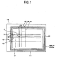
- FIG. 1 illustrates plan view of a first substrate in a liquid crystal display device according to a first embodiment
- FIG. 2 is an enlarged view of a part A in FIG. 1 according to the first embodiment
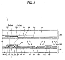
- FIG. 3 is a sectional view , taken along III-III in FIG 1 ;
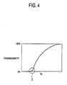
- FIG. 4 graphs a transmissivity attribute as a function of pixel voltage in the liquid crystal display device according to the first embodiment
- FIG. 5 shows a schematic of an equivalent circuit of a pixel of the liquid crystal display device according to the first embodiment
- FIGS. 6A to 6C illustrate brightness irregularity due to delayed gate signals
- FIG. 7 is an enlarged view of a part B in FIG. 1 according to the first embodiment
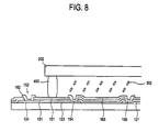
- FIG. 8 is a sectional view, taken along line VIII-VIII in FIG. 7 ;
- FIG. 9 illustrates an improvement of brightness irregularity in the liquid crystal display device according to the first embodiment
- FIG. 10 illustrates a relation between delayed gate signals and brightness
- FIG. 11 illustrates a variation of a parasitic capacitance and brightness
- FIG. 12 illustrates a delay of the gate signal due to a resistance value of a resistor
- FIG. 13 illustrates a pixel voltage depending on the resistance value of the resistor
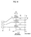
- FIG. 14 illustrates a circuit diagram of main parts in a liquid crystal display device according to a second exemplary embodiment
- FIG. 15 is an enlarged view of a part C in FIG. 14 ;
- FIG. 16 illustrates a liquid crystal display device according to a third embodiment
- FIG. 17 is a sectional view, taken along line XVII-XVII in FIG. 16 ;
- FIG. 18 is an equivalent circuit of a pixel in a liquid crystal display device according to a fourth embodiment.
- FIG. 19 illustrates a principle of improving visibility in the liquid crystal display device according to the fourth embodiment
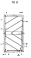
- FIG. 20 illustrates an arrangement of the liquid crystal display device according to the fourth embodiment.
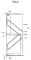
- FIG. 21 illustrates an arrangement of a liquid crystal display device according to a fifth embodiment.
- first film i.e., a layer
- second film i.e., a layer
- discussion regarding forming a first film (i.e., a layer) "on” or “above” a second film (i.e., a layer) is to be understood as covering situations where a third layer is disposed between the two films (i.e., layers) as well as that where the two films (i.e., layers) directly contact each other.
- a liquid crystal display device will be described with reference to FIGS. 1 to 3 .
- a liquid crystal display device 1 ( Fig. 3 ) includes a first substrate 100 which has a thin film transistor T, a second substrate 200 which is spaced apart from and faces the first substrate 100, a liquid crystal material layer 300 which is disposed between the first and second substrates 100 and 200 and a sealant ring 400 ( Fig. 1 ) which sealably joins the first and second substrates 100 and 200 to one another in spaced apart relation.
- the first substrate 100 includes a display region and a non-display region which surrounds the display region.
- a gate main line 121 of the display region is connected with a gate pad 124 through a fan-out part 123 of the non-display region.
- a gate signal is transmitted from a signal origination pad (e.g., IC connection pad, see 124 of Fig. 7 ) to.gate electrode over a gate wire where the latter wire is formed on a first insulating substrate 111.
- the gate wire may include a single or plural metal layers.
- the gate wire generally includes the gate main line 121 which is disposed in the display region and extends transversely, the gate electrode 122 which is connected with the gate main line 121, the fan-out part 123 which extends from the gate main line 121 to the non-display region, and the gate pad 124 which is connected with an end part of the fan-out part 123.
- a storage electrode line 125 often extends in parallel with the gate main line 121 as seen for example in Fig. 2 .
- the gate signal origination pad 124 is often connected with a packaging terminal or IC pin of a gate driver circuit (not shown) that outputs the gate signal to the pad end of the gate wire.
- the gate pad 124 has a substantially wider width than the gate main line 121 that connects that signal sourcing pad 124 to the gates of TFT's distributed along the gate main line 121.
- a gate insulating layer 131 which in one embodiment is made of a silicon nitride (SiN x ) overlaps the gate electrode 122 and the gate wire 121 where the latter (121, 122) are disposed on the first insulating substrate 111.
- a semiconductor layer 132 which in one embodiment includes amorphous silicon (a-Si) is formed on the gate insulating layer 131 overlapping the gate electrode 122.
- An ohmic contact layer 133 which in one embodiment includes n+ hydrogenated amorphous silicon highly doped with an n-type dopant is formed on the semiconductor layer 132. The ohmic contact layer 133 is selectively removed (etched away) from a channel between a source electrode 142 and a drain electrode 143 of the TFT (T).
- a data carrying wire is formed to extend over the drain's ohmic contact layer 133 and on top of the gate insulating layer 131.
- the data wire may include a single or multiple layers of metal.
- the data wire includes a data line 141 which is shown extending vertically in Fig. 2 and crosses the gate main line 121 at a corner portion of the pixel area.
- the source electrode 142 branches out from the data line 141 and extends over the ohmic contact layer 133.
- the drain electrode 143 which is separated from the source electrode 142, extends over the ohmic contact layer 133 opposite to the source electrode 142.
- a fan-out part 144 of the source line extends from the data main line 141 to the non-display region and a data drive pad 145 (belonging to a data driving circuit or IC, not shown) which is connected with an end of the fan-out part 144.
- the data pad 145 is connected with a data driver circuit (not shown) and receives a data driving signal.
- the data pad 145 has a wider width than the data main line 141.
- a passivation layer 151 is formed on the data wire and the semiconductor layer 132 that is not covered by the data wire.
- a contact hole 152 is formed on the passivation layer 151 to expose the drain electrode 143 therethrough.
- contact holes 153, 154 and 155 are also formed on the passivation layer 151.
- the gate insulating layer 131 is removed from the contact holes 153, 154 and 155.
- a pixel electrode 161 is formed on the passivation layer 151.
- the pixel electrode 161 is typically made of a transparent conductive material such as indium tin oxide (ITO), indium zinc oxide (IZO), etc.
- the pixel electrode 161 is connected with the drain electrode 143 through the contact hole 152.
- a pixel electrode splitting pattern 166 is defined (cut through) the pixel electrode 161 as shown.
- the pixel electrode cutting pattern 166 of the pixel electrode 161 divides the liquid crystal layer 300 into a plurality of regions, together with a common electrode cutting pattern 252 (to be described later).
- a black matrix 221 is formed on a second insulating substrate 211.
- the black matrix 221 generally outlines a corresponding red, green or blue filter 231 and blocks light from being directly emitted through the area of the underlying thin film transistor (T) of the first substrate 100.
- the black matrix 221 may include a photoresist organic material added with a black pigment.
- the black pigment may include carbon black or titanium oxide.
- a color filter 231 may include a bandpassing optical material such as one of red, green and blue filters that are repeatedly formed between areas of the black matrix 221.
- the color filter 231 assigns color to light emitted from a backlight unit (not shown) and traveling through the liquid crystal layer 300.
- the color filter 231 typically includes a photoresist organic material.
- An overcoat, planarizing layer 241 is typically formed on the color filter 231 and the black matrix 221.
- the overcoat layer 241 provides planar surface even though the filter and matrix are of different thicknesses and the overcoat layer 241 protects the color filter 231.
- the overcoat layer 241 may include a photoresist acrylic resin.
- a common electrode 251 is formed on the overcoat layer 241.
- the common electrode 251 includes a transparent conductive material such as indium tin oxide (ITO), indium zinc oxide (IZO), etc.
- ITO indium tin oxide
- IZO indium zinc oxide
- the common electrode 251 supplies a voltage to one side of the liquid crystal material layer 300, while the pixel electrode 161 of the thin film transistor substrate provides a second voltage to the other side so as to establish one or more electric filed patterns through the liquid crystal material layer 300.
- the common electrode cutting pattern 252 is formed on the common electrode 251.
- the common electrode cutting pattern 252 divides the liquid crystal layer 300 into a plurality of regions together with the pixel electrode cutting pattern 166 of the pixel electrode 161.
- the pixel electrode cutting pattern 166 and the common electrode cutting pattern 252 are not limited to the V-shaped ones illustrated for the first embodiment, and may be, otherwise, formed in various shapes. In another embodiment of the present disclosure, a protrusion may be provided to divide the liquid crystal layer 300 into a plurality of regions instead of the cutting patterns 166 and 252.
- the liquid crystal layer 300 is disposed between the first and second substrates 100 and 200.
- the liquid crystal material layer 300 is a vertically aligned (VA) mode, in which a long axis of liquid crystal molecules is perpendicular to the first and second substrates 100 and 200 if not receiving a voltage.
- VA vertically aligned
- the liquid crystal molecules may lie irregularly in all directions since the lying direction is not determined by boundary conditions, thereby creating a disclination line on a boundary between different lying directions.
- the cutting patterns are organized 166 and 252 to form a fringe electric field when a voltage is supplied to the liquid crystal layer 300 and to thereby determine the lying direction of the liquid crystal molecules.
- the liquid crystal layer 300 is divided into plural regions by the cutting patterns 166 and 252.
- the liquid crystal display device 1 has a normally black mode when no substantial voltage is applied across the liquid crystal material, and a transmissivity that is a function of the pixel voltage as is illustrated in the plot of FIG. 4 .
- the transmissivity variation in a low gradation shown in a part C in FIG. 4 is three times more drastic for the VA material than a twisted nematic liquid crystal.
- the gate main line 121 receives a gate signal through the gate pad 124 connected with the end part thereof. Due to a resistance of the gate main line 121, the thin film transistor T adjacent to the gate pad 124, i.e., a left thin film transistor T receives a short-delayed gate signal but the thin film transistor T far from the gate pad 123, i.e., a right thin film transistor T receives a longer-delayed gate signal.
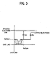
- the kick back voltage Vkb may be expressed by a formula 1 as follows.
- V kb V on - V off * C p / C lc + C st + C p
- Cp refers to combined parasitic capacitance Cgs between the gate electrode and the source electrode and a parasitic capacitance Cgd between the gate electrode and the drain electrode
- Clc is a liquid crystal capacitance
- Cst is a storage capacitance
- Von is a gate on voltage
- Voff means a gate turn-off voltage.
- the gate-on voltage (Von) is not supplied in time, thereby decreasing the kick back voltage Vkb.
- the kick back voltage Vkb becomes larger when a negative pixel voltage is supplied rather than when a positive pixel voltage is supplied.
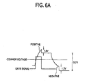
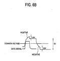
- FIGS. 6A and 6B respectively illustrate a kick back voltage Vkb of a pixel in a left-side display region having a short-delayed gate signal, and a pixel in a right-side display region having a longer-delayed gate signal.
- the kick back voltage is about 1.0V when the positive pixel voltage is supplied while it is about 1.2V when the negative pixel voltage is supplied.
- the kick back voltage is about 0.8V when both the positive pixel voltage and the negative pixel voltage are supplied.
- the left-side pixel has a larger root mean square pixel voltage that remains ultimately, and an image corresponding to the left-side pixel is seen as being comparatively brighter.
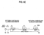
- the gate signal is shorter-delayed and the kick back voltage Vkb becomes larger if they are closer to the gate pad 124. Conversely, the gate signal is longer-delayed and the kick back voltage Vkb becomes smaller if they are farther from the gate pad 124.
- the left-side pixel has a larger root mean square pixel voltage than the right pixel to brighten the image corresponding to the left pixel more than that corresponding to the right pixel.
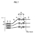
- the liquid crystal display device 1 according to the first embodiment of the present disclosure provides a compensating resistor 163 disposed between the gate main line 121 and the fanout line 123 (and the gate pad 124) to reduce the above-mentioned problem.
- the resistor 163 is disposed between the fan-out part 123 and the gate main line 121 in the non-display region.
- the primary resistive material of resistor 163 is provided by the same layer that provides the primary material of the pixel electrode 161.
- the resistor 163 includes a first part 163a which is connected with the fan-out part 123, a second part 163b which is connected with the gate main line 121 and a third part 163c which is electrically disposed between the first and second parts 163a and 163b.
- the first part 163a contacts the fan-out part 123 through the contact hole 154.
- the second part 163b contacts the gate main line 121 through the contact hole 155.
- the gate pad 124 exposed by the contact hole 153 is covered by a contact member 162, where member 162 is comprised of the same material as that of the pixel electrode 161 and where member 162 is disposed in the same layer with the pixel electrode 161.
- the resistor 163 can include one or more of optically transmissive electrical conductors such as indium tin oxide (ITO), indium zinc oxide (IZO), etc., which have a larger resistance than an optically opaque electrical conductor such as the metal material used in the gate main line 121. Due to the resistor 163 having a substantially large resistance, the gate signal is substantially delayed before entering the display region, as shown in FIG. 9 and the difference in delay as shown by Figs. 6A-6B is no longer a substantial factor in determining kick back.
- optically transmissive electrical conductors such as indium tin oxide (ITO), indium zinc oxide (IZO), etc.
- total resistance of the gate main line 121 is typically 4000 ⁇ to 7000 ⁇ while a total resistance of the resistor 163 may be 10% to 50% of the total resistance of the gate main line 121.
- the resistance value of the resistor 163 may vary by changing one or more of a thickness, width and length attribute of the resistor 163.
- the resistance value of the resistor 163 be set so that the gate signal delay variation due to resistance of the main gate line is substantially less than gate signal delay to total wire resistance.
- the gate signal delay value of a far right pixel of the display region is no more than about twice the gate signal delay value of the far left pixel in the display region (the one closest to the gate signal originating pad 124.
- the distance between the gate main line 121 and the gate pad 124 is various, thereby causing a different resistance therebetween and irregular brightness.
- the length of the third part 163c in the resistor 163 is in inverse proportion to the distance between the corresponding gate main line 121 and the gate pad 124.
- brightness irregularity due to variation in distance between the gate main line 121 and the gate pad 124 decreases.
- the sealant 400 is disposed on the fan-out part 123 while the resistor 163 is provided inside the liquid crystal material containing area of the sealant 400. Because the resistor 163 is not exposed to the outside, it is safe from being corroded.
- a flow of static electricity from the outside may damage the thin film transistor T.
- a substantial portion of the energy of the static electricity flow introduced from the gate pad 124 is dissipated in the resistor 163 having the larger resistance, thereby reducing problems due to static electricity.
- a resistor 163 according to another embodiment of the present disclosure may include other materials having a larger resistance than the gate main line 121 and being different from the material of the pixel electrode 161.
- the shape of the resistor 163 is identical and the distance differences between the gate main line 121 and the gate pad 124 may be dealt with by changing the shape of the fan-out part 123.
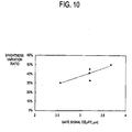
- FIG. 10 illustrates a brightness variation ratio depending on the gate signal delay value in the display region.
- BVR (Brightness of the left display region - Brightness of central display region)/(Brightness of central display region)*100.
- a large value means a large brightness difference.
- the brightness variation ratio (BVR) increases around 64% (from 30.6% to 50.3%)
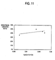
- FIG. 11 illustrates a brightness variation ratio according to Cp/(C1c+Cst+Cp) in proportion to the kick back voltage. As shown therein, if Cp/(C1c+Cst+Cp) increases 24% (from 0.037 to 0.046), the brightness variation ratio rises approximately 26.4% (from 35.6% to 45%).
- brightness irregularity gets worse as variation in the gate signal delay value gets larger and/or as comparative contribution to kickback from the parasitic capacitance gets larger.
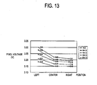
- the comparative amount of gate signal delay relative to position of the pixel electrode can be made to vary by changing a compensating or ballasting resistance in the non-display region, i.e., a resistance from the gate pad to the gate main line, which will be described with reference to the examples of FIGS. 12 and 13 .
- the resistance in the non-display region was switched over the following four values: 1/6k ⁇ , 1/3k ⁇ , 1/2k ⁇ and 2/3k ⁇ .
- the bottom most data plot having 0k ⁇ is the case where there is no ballasting resistor and a gate main line and a gate pad are integrally formed in the same layer.
- the increased resistance of the ballasting resistor in the non-display region decreases the positionally-related differences in the gate signal delay and the positionally-related differences in the pixel voltage between the left-side display region and the right-side display region.
- the resistance of the ballasting resistor in the non-display region becomes larger, it also becomes more difficult to transmit a strong gate signal to each TFT.
- the resistance of the ballasting resistor should be determined as a compromise and in consideration of the total resistance of the gate main line 121.
- FIG. 14 illustrates a part corresponding B area in FIG. 1 .
- an anti-static set of diode-connected MOSFETs 170 is formed on an outer circumference portion of each ballasting resistor 163.
- the anti-static set 170 is electrically connected with a gate outer circumference and a common voltage line 146. If static electricity is introduced through a gate pad 124 during a manufacturing process, the resistor 163 having a large resistance may be damaged, thereby causing disconnection. However, the anti-static set of diode-connected MOSFETs 170 is activated when the absolute value of voltage of the static exceed a predefined threshold and the activated set 170 scatters the introduced static electricity to the common voltage line (e.g., ground) 146 to prevent the resistor 163 from being damaged.
- the gate outer circumference portion refers a gate wire connected with the gate main line 121 and formed outside of the resistor 163. That is, the gate outer circumference portion includes the gate pad 124 and the fan-out part 123.
- the anti-static diode means 170 includes a plurality of thin film MOSFET transistors.
- the anti-static diode means 170 includes a first diode-connected MOSFET 171 and a second diode-connected MOSFET 172 coupled for carrying differently directed current flows.
- the first diode-connected MOSFET 171 is provided so that a negative going current flows from the gate outer circumference to the common voltage line 146.
- the second diode-connected MOSFET 172 is provided so that a positive-going current flows from the common voltage line 146 to the gate outer circumference portion.
- the common voltage line 146 serves as an electrostatic bar with respect to the anti-static diode means 170.
- a control terminal (gate) 1711 and an input terminal (drain) 1712 of the first diode-connected MOSFET 171 are connected with each other and with the gate line outer circumference (121).
- An output terminal (source) 1713 of the first diode-connected MOSFET 171 is connected with the common voltage line 146.
- a bridge 1714 connects the input terminal (drain) 1712 to the gate outer circumference (121). If static electricity is inputted to the gate outer circumference and the static exceeds the predefined threshold (Vt) of MOSFET 171, the control terminal 1711 connected with the gate outer circumference is switched to a turned on state, MOSFET 171 becomes conductive and thereby diverts the static electricity to the common voltage line 146 connected with the output terminal 1713.
- a control terminal (gate) 1721 and an input terminal (drain) 1722 of the second diode-connected MOSFET 172 are connected with the common voltage line 146.
- An output terminal (source) 1723 of the second diode-connected MOSFET 172 is connected with the gate outer circumference (121).
- a second bridge 1724 connects the common voltage line 146 and the control terminal 1721 while a third bridge 1725 connects the output terminal 1723 and the gate outer circumference.
- MOSFET 172 If static electricity is inputted to the gate outer circumference and the static exceeds the predefined threshold (Vt) of MOSFET 172, the control terminal 1721 connected with the gate outer circumference through the bridge 1724 is switched to a turned-on state, MOSFET 172 becomes conductive and thereby diverts the static electricity to the common voltage line 146 connected with the input terminal (drain) 1722.
- Vt predefined threshold
- the anti-static diode means 170 may include only a first anti-static diode-connected MOSFET 171 without the second anti-static diode-connected MOSFET 172.
- a gate pad 164 and a fan-out part 165 according to the third embodiment are integrally formed in a same layer with the ballasting resistor 163.
- the gate pad 164 and the fan-out part 165 may include indium tin oxide (ITO) or indium zinc oxide (IZO).
- the resistor 163 is connected with a gate main line 121 through a contact hole 156.
- the gate pad 164 and the fan-out part 165 perform the same operation as the resistor 163 according to the first embodiment.
- the resistance of the ballasting resistor 163 is in inverse proportion to a distance between the corresponding gate main line 121 and the gate pad 164 as was the case for one version of the first embodiment.
- brightness irregularity due to a distance difference between the gate main line 121 and the gate pad 164 decreases.
- only a fan-out part 165 composed of a substantially resistive material such as indium tin oxide (ITO) or indium zinc oxide (IZO) may be provided to delay a corresponding gate signal, without forming a separate ballasting resistor 163 in the shape of the square waves such as shown in the lower two lines of Fig. 16 .
- ITO indium tin oxide
- IZO indium zinc oxide
- a liquid crystal display device according to a fourth embodiment will be described with reference to FIGS. 18 to 20 .
- a thin film transistor T is connected with two liquid crystal capacitances C LC1 and C LC2 .
- the first liquid crystal capacitance C LC1 is formed between a first pixel electrode PE1 and a common electrode CE.
- the fist pixel electrode PE1 is directly connected with the thin film transistor T.
- the second liquid crystal capacitance C LC2 is formed between the second pixel electrode PE2 and the common electrode CE.
- the second pixel electrode PE2 is indirectly connected with the thin film transistor T through a coupling capacitance C CP .
- first pixel electrode PE1 and the second pixel electrode PE2 are electrically separated from each other due to the presence of coupling capacitance C cp and the second liquid crystal capacitance C LC2 .
- the liquid crystal display device according to the fourth embodiment can improve visibility per a mechanism which will be described with reference to FIG. 19 .
- the first pixel electrode PE1 receives a data signal through the thin film transistor T.
- the second pixel electrode PE2 receives a data signal by a voltage through a coupling capacitance C CP formed in an insulating layer between the second pixel electrode PE and the thin film transistor T, instead of directly receiving the data signal from the thin film transistor T.
- the second pixel electrode PE2 receives a weaker signal than the first pixel electrode PE1, thereby causing a difference in brightness of the pixel region corresponding to the first pixel electrode PE1 and the pixel region corresponding to the second pixel electrode PE2.
- the voltage supplied to the second pixel electrode PE2 is 50% to 90% of the voltage supplied to the first pixel electrode PE1.
- a single pixel has a plurality of regions that have different gamma curves.
- the brightness and color in a front and lateral parts are compensated to improve lateral visibility.
- the pixel electrode 161 includes a first pixel electrode 161a and a second pixel electrode 161b which are separated from each other by a pixel electrode separating pattern 167.
- the second pixel electrode 161b has a trapezoid shape whose three sides are surrounded by the first pixel electrode 161a.
- a pixel electrode cutting pattern 166 which is side by side with the pixel electrode separating pattern 167 is formed on the first and second pixel electrodes 161a and 161b.
- a drain electrode 143 includes a first drain electrode 143a which is connected with the first pixel electrode 161a and supplies an electrical signal thereto and a second drain electrode 143b which extends below the second pixel electrode 161b.
- the second drain electrode 143b forms a coupling capacitance C cp together with the second pixel electrode 161b.
- the pixel electrode separating pattern 167 and the pixel electrode cutting pattern 166 divide a liquid crystal layer 300 into a plurality of regions together with a common electrode cutting pattern 252.
- a storage electrode line 125 is formed along the boundary of the pixel electrode 161. Upper and lower storage electrode lines 125 are connected with each other through a contact hole 157 and a bridge electrode 168.
- a liquid crystal display device according to a fifth embodiment of the present disclosure will be described with reference to FIG. 21 .
- a pixel electrode 161 has a rectangular shape as a whole.
- the pixel electrode 161 is elongated in an extension direction of a data line 141.
- the pixel electrode 161 includes a first pixel electrode 161a and a second pixel electrode 161b which are separated from each other by a pixel electrode separating pattern 167.
- the first pixel electrode 161a is disposed in a center of a pixel and has a chevron-shape.
- the second pixel electrode 161b surrounds an inside, an upper part and a lower part of the first pixel electrode 161a.
- the second pixel electrode 161b is larger than the first pixel electrode 161a.
- a thin film transistor T includes a first thin film transistor TFT1 which is connected with the first pixel electrode 161a and a second thin film transistor TFT2 which is connected with the second pixel electrode 161b.
- a drain electrode 143 of the respective thin film transistors TFT1 and TFT2 overlaps the pixel electrode 161 to form a storage capacitance Cst.
- the storage capacitance Cst is proportional to an overlapping size of the drain electrode 143 and the pixel electrode 161.
- respective pixel electrodes 161a and 161b receive different pixel voltages by using independent thin film transistors TFT1 and TFT2.
- the method of improving visibility in the fifth embodiment is the same as that in the fourth embodiment. Thus the detailed description will not be provided here.
- the configuration of the non-display region in the fourth and fifth embodiments can be the same as that in the first to third embodiment of the present disclosure.
- the liquid crystal capacitance Clc and the storage capacitance Cst are small.
- the kick back voltage Vkb becomes larger, thereby making the brightness difference (refer to Formula 1) more significant.
- the present disclosure of invention provides a liquid crystal display device which reduces a brightness irregularity due to a gate signal delay difference.
Description
- The present disclosure of invention relates to a liquid crystal display (LCD) device, and more particularly, to a liquid crystal display device in which delay differences of gate signal transmission paths are reduced and brightness uniformity is thereby improved.
- A typical liquid crystal display device includes a first substrate (TFT-containing substrate) which has a plurality of thin film transistors (TFT's), a second substrate (common electrode substrate) which is in spaced apart facing relation with the first substrate and a liquid crystal material layer which is disposed between the first and second substrates.
- Pixel areas of the TFT-containing substrate (first substrate) are typically defined as rectangular areas having corners located at or near where a corresponding gate line and a data line disposed in the TFT substrate cross each other. Light transmission through each pixel area is typically controlled by a thin film transistor (TFT) having its gate connected to the gate line, its source connected to the data line and its drain connected to a corresponding pixel-electrode of the pixel area. When a pixel-activating gate signal, i.e., a gate turn-on voltage (Von), is supplied to the gate line, the thin film transistor is turned on and a data voltage (Vd) appearing at its source is charged to the pixel electrode through the conductive channel region of the TFT.
- An electric field which is formed due to the difference between a pixel voltage Vp appearing on the pixel electrode and a common voltage Vcom appearing on the spaced apart common electrode of the second substrate, drives the liquid crystal material in between to a corresponding optical orientation. In some embodiments, the polarity of the data voltage Vd supplied on the data lines flips with every frame or with predefined numbered ones of frames so as to reduce undesired effects of unidirectional current flow.
- A number of factors can cause the Vp voltage appearing on the pixel-electrode to be different than the Vd voltage supplied on the data lines. So-called Miller capacitances or parasitic capacitances, Cp are often present between the gate of each TFT and each of its source and drain electrodes. The rising and falling edges of the data voltage pulse, Vd supplied to the pixel areas via the TFT are stunted (caused to change more slowly) due to negative feedback through the parasitic capacitances Cp, thereby causing a different pixel voltage, Vp to appear on the charged pixel-electrode as compared to the Vd magnitude of the data voltage pulse appearing on the data line. The difference between the magnitude of data voltage Vd supplied on the data line and the pixel voltage Vp developed on the pixel-electrode is referred to as a kick back voltage, Vkb.
- Another factor that affects the pixel-electrode voltage, Vp is the magnitude of the gate turn-on voltage applied to the gate of the TFT. In one class of embodiments, the gate line receives its gate signal from a wider gate signal origination pad, where multiple pads crowd together in a region where a corresponding driving chip (integrated circuit chip) may be disposed and each gate line functions as a separate signal transmission strip for coupling the gate signal from its IC connection pad to individual TFT's distributed along each gate line. Pixel areas which are positioned closer to their respective gate distribution pad generally receive a short-delayed gate signal (delayed due to RC factors) while pixel areas which are positioned farther from the gate pad receive a longer-delayed gate signal due to the cumulative resistance (R) and/or other transmission line effects (i.e., C and/or L) of the gate line.
- The size of the kick back voltage Vkb depends, among other things, on the delay-producing cumulative resistance of the gate signal. The resulting pixel voltage, Vp is affected by the variation of the kick back voltage Vkb, thereby causing irregular brightness in an image due to distance of pixel area from its corresponding gate signal originating pad. These effects may cause undesirable degradation of image quality.
JP 04313733 claim 1.
US 2003/0227078 A1 discloses a liquid crystal display device with capacitive or resistive means to compensate the difference in gate lines resistances caused by varying lengths of the fan-out parts from the gate main lines to the respective gate pads.
US2006/0114209 A1 ,US2005/0018121 A1 andUS 2004/0135956 A1 each disclose an LCD device having a ballast electric resistor of a zigzag pattern in the fan-out parts from the gate main lines to the respectitive gate pads in order to compensate the difference in lengths of the gate lines. - The present invention provides a liquid crystal display device according to appended
claim 1 in order to reduce brightness irregularity due to delay differences between gate signals. - Additional aspects of the invention are set forth in the appended dependent claims 2-14.
- The above and/or other aspects and advantages of the disclosure will become more readily appreciated from the following detailed description taken in conjunction with the accompanying drawings of which:
-
FIG. 1 illustrates plan view of a first substrate in a liquid crystal display device according to a first embodiment; -
FIG. 2 is an enlarged view of a part A inFIG. 1 according to the first embodiment; -
FIG. 3 is a sectional view , taken along III-III inFIG 1 ; -
FIG. 4 graphs a transmissivity attribute as a function of pixel voltage in the liquid crystal display device according to the first embodiment; -
FIG. 5 shows a schematic of an equivalent circuit of a pixel of the liquid crystal display device according to the first embodiment; -
FIGS. 6A to 6C illustrate brightness irregularity due to delayed gate signals; -
FIG. 7 is an enlarged view of a part B inFIG. 1 according to the first embodiment; -
FIG. 8 is a sectional view, taken along line VIII-VIII inFIG. 7 ; -
FIG. 9 illustrates an improvement of brightness irregularity in the liquid crystal display device according to the first embodiment; -
FIG. 10 illustrates a relation between delayed gate signals and brightness; -
FIG. 11 illustrates a variation of a parasitic capacitance and brightness; -
FIG. 12 illustrates a delay of the gate signal due to a resistance value of a resistor; -
FIG. 13 illustrates a pixel voltage depending on the resistance value of the resistor; -
FIG. 14 illustrates a circuit diagram of main parts in a liquid crystal display device according to a second exemplary embodiment; -
FIG. 15 is an enlarged view of a part C inFIG. 14 ; -
FIG. 16 illustrates a liquid crystal display device according to a third embodiment; -
FIG. 17 is a sectional view, taken along line XVII-XVII inFIG. 16 ; -
FIG. 18 is an equivalent circuit of a pixel in a liquid crystal display device according to a fourth embodiment; -
FIG. 19 illustrates a principle of improving visibility in the liquid crystal display device according to the fourth embodiment; -
FIG. 20 illustrates an arrangement of the liquid crystal display device according to the fourth embodiment; and -
FIG. 21 illustrates an arrangement of a liquid crystal display device according to a fifth embodiment. - DETAILED DESCRIPTION OF EMBODIMENTS
- Hereinafter, embodiments in accordance with the disclosure will be described with reference to accompanying drawings, wherein like numerals often refer to like elements and repetitive descriptions may then be avoided where practical.
- Hereinafter, discussion regarding forming a first film (i.e., a layer) "on" or "above" a second film (i.e., a layer) is to be understood as covering situations where a third layer is disposed between the two films (i.e., layers) as well as that where the two films (i.e., layers) directly contact each other.
- A liquid crystal display device according to the present disclosure will be described with reference to
FIGS. 1 to 3 . - A liquid crystal display device 1 (
Fig. 3 ) includes afirst substrate 100 which has a thin film transistor T, asecond substrate 200 which is spaced apart from and faces thefirst substrate 100, a liquidcrystal material layer 300 which is disposed between the first andsecond substrates Fig. 1 ) which sealably joins the first andsecond substrates - The
first substrate 100 includes a display region and a non-display region which surrounds the display region. A gatemain line 121 of the display region is connected with agate pad 124 through a fan-outpart 123 of the non-display region. - Hereinafter, the
first substrate 100 according to the first embodiment will be described. - A gate signal is transmitted from a signal origination pad (e.g., IC connection pad, see 124 of
Fig. 7 ) to.gate electrode over a gate wire where the latter wire is formed on a firstinsulating substrate 111. The gate wire may include a single or plural metal layers. The gate wire generally includes the gatemain line 121 which is disposed in the display region and extends transversely, thegate electrode 122 which is connected with the gatemain line 121, the fan-outpart 123 which extends from the gatemain line 121 to the non-display region, and thegate pad 124 which is connected with an end part of the fan-outpart 123. Astorage electrode line 125 often extends in parallel with the gatemain line 121 as seen for example inFig. 2 . - The gate
signal origination pad 124 is often connected with a packaging terminal or IC pin of a gate driver circuit (not shown) that outputs the gate signal to the pad end of the gate wire. Thegate pad 124 has a substantially wider width than the gatemain line 121 that connects that signal sourcingpad 124 to the gates of TFT's distributed along the gatemain line 121. - A
gate insulating layer 131 which in one embodiment is made of a silicon nitride (SiNx) overlaps thegate electrode 122 and thegate wire 121 where the latter (121, 122) are disposed on the firstinsulating substrate 111. - A
semiconductor layer 132 which in one embodiment includes amorphous silicon (a-Si) is formed on thegate insulating layer 131 overlapping thegate electrode 122. Anohmic contact layer 133 which in one embodiment includes n+ hydrogenated amorphous silicon highly doped with an n-type dopant is formed on thesemiconductor layer 132. Theohmic contact layer 133 is selectively removed (etched away) from a channel between asource electrode 142 and adrain electrode 143 of the TFT (T). - A data carrying wire is formed to extend over the drain's
ohmic contact layer 133 and on top of thegate insulating layer 131. The data wire may include a single or multiple layers of metal. The data wire includes adata line 141 which is shown extending vertically inFig. 2 and crosses the gatemain line 121 at a corner portion of the pixel area. The source electrode 142 branches out from thedata line 141 and extends over theohmic contact layer 133. Thedrain electrode 143 which is separated from thesource electrode 142, extends over theohmic contact layer 133 opposite to thesource electrode 142. A fan-outpart 144 of the source line extends from the datamain line 141 to the non-display region and a data drive pad 145 (belonging to a data driving circuit or IC, not shown) which is connected with an end of the fan-outpart 144. - The
data pad 145 is connected with a data driver circuit (not shown) and receives a data driving signal. Thedata pad 145 has a wider width than the datamain line 141. - A
passivation layer 151 is formed on the data wire and thesemiconductor layer 132 that is not covered by the data wire. Acontact hole 152 is formed on thepassivation layer 151 to expose thedrain electrode 143 therethrough. As shown inFIGS. 7 and8 , contact holes 153, 154 and 155 are also formed on thepassivation layer 151. Thegate insulating layer 131 is removed from the contact holes 153, 154 and 155. - A
pixel electrode 161 is formed on thepassivation layer 151. Thepixel electrode 161 is typically made of a transparent conductive material such as indium tin oxide (ITO), indium zinc oxide (IZO), etc. Thepixel electrode 161 is connected with thedrain electrode 143 through thecontact hole 152. A pixelelectrode splitting pattern 166 is defined (cut through) thepixel electrode 161 as shown. - The pixel
electrode cutting pattern 166 of thepixel electrode 161 divides theliquid crystal layer 300 into a plurality of regions, together with a common electrode cutting pattern 252 (to be described later). - Hereinafter, the
second substrate 200 of the liquidcrystal display device 1 according to the first embodiment will be described. - A
black matrix 221 is formed on a second insulatingsubstrate 211. Theblack matrix 221 generally outlines a corresponding red, green orblue filter 231 and blocks light from being directly emitted through the area of the underlying thin film transistor (T) of thefirst substrate 100. Theblack matrix 221 may include a photoresist organic material added with a black pigment. The black pigment may include carbon black or titanium oxide. - A
color filter 231 may include a bandpassing optical material such as one of red, green and blue filters that are repeatedly formed between areas of theblack matrix 221. Thecolor filter 231 assigns color to light emitted from a backlight unit (not shown) and traveling through theliquid crystal layer 300. Thecolor filter 231 typically includes a photoresist organic material. - An overcoat,
planarizing layer 241 is typically formed on thecolor filter 231 and theblack matrix 221. Theovercoat layer 241 provides planar surface even though the filter and matrix are of different thicknesses and theovercoat layer 241 protects thecolor filter 231. Theovercoat layer 241 may include a photoresist acrylic resin. - A
common electrode 251 is formed on theovercoat layer 241. Thecommon electrode 251 includes a transparent conductive material such as indium tin oxide (ITO), indium zinc oxide (IZO), etc. Thecommon electrode 251 supplies a voltage to one side of the liquidcrystal material layer 300, while thepixel electrode 161 of the thin film transistor substrate provides a second voltage to the other side so as to establish one or more electric filed patterns through the liquidcrystal material layer 300. - The common
electrode cutting pattern 252 is formed on thecommon electrode 251. The commonelectrode cutting pattern 252 divides theliquid crystal layer 300 into a plurality of regions together with the pixelelectrode cutting pattern 166 of thepixel electrode 161. The pixelelectrode cutting pattern 166 and the commonelectrode cutting pattern 252 are not limited to the V-shaped ones illustrated for the first embodiment, and may be, otherwise, formed in various shapes. In another embodiment of the present disclosure, a protrusion may be provided to divide theliquid crystal layer 300 into a plurality of regions instead of the cuttingpatterns - The
liquid crystal layer 300 is disposed between the first andsecond substrates crystal material layer 300 is a vertically aligned (VA) mode, in which a long axis of liquid crystal molecules is perpendicular to the first andsecond substrates - If the cutting
patterns liquid crystal layer 300 and to thereby determine the lying direction of the liquid crystal molecules. Theliquid crystal layer 300 is divided into plural regions by the cuttingpatterns - The liquid
crystal display device 1 according to the first embodiment has a normally black mode when no substantial voltage is applied across the liquid crystal material, and a transmissivity that is a function of the pixel voltage as is illustrated in the plot ofFIG. 4 . The transmissivity variation in a low gradation shown in a part C inFIG. 4 is three times more drastic for the VA material than a twisted nematic liquid crystal. - In the liquid
crystal display device 1 according to the first embodiment, the gatemain line 121 receives a gate signal through thegate pad 124 connected with the end part thereof. Due to a resistance of the gatemain line 121, the thin film transistor T adjacent to thegate pad 124, i.e., a left thin film transistor T receives a short-delayed gate signal but the thin film transistor T far from thegate pad 123, i.e., a right thin film transistor T receives a longer-delayed gate signal. - Variations in image brightness depending on delay differences of the gate signals are described with reference to
FIGS. 5 to 6C . - The kick back voltage Vkb may be expressed by a
formula 1 as follows. -
Formula 1 -

- As shown in
FIGS. 3 and5 , Cp refers to combined parasitic capacitance Cgs between the gate electrode and the source electrode and a parasitic capacitance Cgd between the gate electrode and the drain electrode, Clc is a liquid crystal capacitance, Cst is a storage capacitance, Von is a gate on voltage and Voff means a gate turn-off voltage. - If the gate signal is delayed longer relative to a data pulse on the data line, the gate-on voltage (Von) is not supplied in time, thereby decreasing the kick back voltage Vkb. The kick back voltage Vkb becomes larger when a negative pixel voltage is supplied rather than when a positive pixel voltage is supplied.
-
FIGS. 6A and6B respectively illustrate a kick back voltage Vkb of a pixel in a left-side display region having a short-delayed gate signal, and a pixel in a right-side display region having a longer-delayed gate signal. - Regarding the left-side pixel in
FIG. 6A , the kick back voltage is about 1.0V when the positive pixel voltage is supplied while it is about 1.2V when the negative pixel voltage is supplied. Concerning the right-side pixel inFIG. 6B , the kick back voltage is about 0.8V when both the positive pixel voltage and the negative pixel voltage are supplied. - As a result, the left-side pixel has a larger root mean square pixel voltage that remains ultimately, and an image corresponding to the left-side pixel is seen as being comparatively brighter.
- As shown in
FIG. 6C , the gate signal is shorter-delayed and the kick back voltage Vkb becomes larger if they are closer to thegate pad 124. Conversely, the gate signal is longer-delayed and the kick back voltage Vkb becomes smaller if they are farther from thegate pad 124. Thus, the left-side pixel has a larger root mean square pixel voltage than the right pixel to brighten the image corresponding to the left pixel more than that corresponding to the right pixel. - As described above, brightness is different from left and right sides, thereby sometimes showing as an unintended vertical line. Such a problem is more serious in a large-sized liquid crystal display device which has a long gate
main line 121 and causes a longer-delayed gate signal. - Referring to
Fig. 7 , the liquidcrystal display device 1 according to the first embodiment of the present disclosure provides a compensatingresistor 163 disposed between the gatemain line 121 and the fanout line 123 (and the gate pad 124) to reduce the above-mentioned problem. - Hereinafter, the
resistor 163 of the liquidcrystal display device 1 according to the first embodiment will be described with reference toFIGS. 7 to 9 . - The
resistor 163 is disposed between the fan-outpart 123 and the gatemain line 121 in the non-display region. The primary resistive material ofresistor 163 is provided by the same layer that provides the primary material of thepixel electrode 161. Theresistor 163 includes afirst part 163a which is connected with the fan-outpart 123, asecond part 163b which is connected with the gatemain line 121 and athird part 163c which is electrically disposed between the first andsecond parts - The
first part 163a contacts the fan-outpart 123 through thecontact hole 154. Thesecond part 163b contacts the gatemain line 121 through thecontact hole 155. - The
gate pad 124 exposed by thecontact hole 153 is covered by acontact member 162, wheremember 162 is comprised of the same material as that of thepixel electrode 161 and wheremember 162 is disposed in the same layer with thepixel electrode 161. - The
resistor 163 can include one or more of optically transmissive electrical conductors such as indium tin oxide (ITO), indium zinc oxide (IZO), etc., which have a larger resistance than an optically opaque electrical conductor such as the metal material used in the gatemain line 121. Due to theresistor 163 having a substantially large resistance, the gate signal is substantially delayed before entering the display region, as shown inFIG. 9 and the difference in delay as shown byFigs. 6A-6B is no longer a substantial factor in determining kick back. - Thus, the scope of delay differences between gate signals and the variation of the kick back voltage are reduced. Also, the brightness differences between the left and right sides of the display region decreases.
- In one class of embodiments, total resistance of the gate
main line 121 is typically 4000Ω to 7000Ω while a total resistance of theresistor 163 may be 10% to 50% of the total resistance of the gatemain line 121. The resistance value of theresistor 163 may vary by changing one or more of a thickness, width and length attribute of theresistor 163. - It is preferable but not necessary that the resistance value of the
resistor 163 be set so that the gate signal delay variation due to resistance of the main gate line is substantially less than gate signal delay to total wire resistance. In other words, the gate signal delay value of a far right pixel of the display region is no more than about twice the gate signal delay value of the far left pixel in the display region (the one closest to the gatesignal originating pad 124. - The distance between the gate
main line 121 and thegate pad 124 is various, thereby causing a different resistance therebetween and irregular brightness. - The length of the
third part 163c in theresistor 163 is in inverse proportion to the distance between the corresponding gatemain line 121 and thegate pad 124. Thus, brightness irregularity due to variation in distance between the gatemain line 121 and thegate pad 124 decreases. - As seen in
Fig. 8 , thesealant 400 is disposed on the fan-outpart 123 while theresistor 163 is provided inside the liquid crystal material containing area of thesealant 400. Because theresistor 163 is not exposed to the outside, it is safe from being corroded. - During a manufacturing process, a flow of static electricity from the outside may damage the thin film transistor T. According to the first embodiment, a substantial portion of the energy of the static electricity flow introduced from the
gate pad 124 is dissipated in theresistor 163 having the larger resistance, thereby reducing problems due to static electricity. - A
resistor 163 according to another embodiment of the present disclosure may include other materials having a larger resistance than the gatemain line 121 and being different from the material of thepixel electrode 161. In another embodiment of the present disclosure, the shape of theresistor 163 is identical and the distance differences between the gatemain line 121 and thegate pad 124 may be dealt with by changing the shape of the fan-outpart 123. - Hereinafter, the reason why the gate signal delay is adjusted to improve the brightness irregularity will be described.
-
FIG. 10 illustrates a brightness variation ratio depending on the gate signal delay value in the display region. The brightness variation ratio is defined by the mathematical expression, BVR= (Brightness of the left display region - Brightness of central display region)/(Brightness of central display region)*100. Here, a large value means a large brightness difference. - As shown in the example of
FIG. 10 , if the gate signal delay value rises 43% (from 2.55µs to 3.67µs), the brightness variation ratio (BVR) increases around 64% (from 30.6% to 50.3%) -
FIG. 11 illustrates a brightness variation ratio according to Cp/(C1c+Cst+Cp) in proportion to the kick back voltage. As shown therein, if Cp/(C1c+Cst+Cp) increases 24% (from 0.037 to 0.046), the brightness variation ratio rises approximately 26.4% (from 35.6% to 45%). - As shown in
FIGS. 10 and11 , brightness irregularity (BVR) gets worse as variation in the gate signal delay value gets larger and/or as comparative contribution to kickback from the parasitic capacitance gets larger. - The comparative amount of gate signal delay relative to position of the pixel electrode can be made to vary by changing a compensating or ballasting resistance in the non-display region, i.e., a resistance from the gate pad to the gate main line, which will be described with reference to the examples of
FIGS. 12 and13 . - As shown therein, the resistance in the non-display region was switched over the following four values: 1/6kΩ, 1/3kΩ, 1/2kΩ and 2/3kΩ. The bottom most data plot having 0kΩ is the case where there is no ballasting resistor and a gate main line and a gate pad are integrally formed in the same layer.
- As shown in
FIG. 12 , the larger the resistance of the ballasting resistor in the non-display region was, the higher was the cumulative gate signal delay value when moving from the left side of the main line (closest to the gate pad) to the right side of the main line (farthest from the gate signal originating pad). If the resistance of the ballasting resistor in the non-display region becomes larger, the ratio of the right gate signal delay value over the left gate signal delay value decrease. In other words, change in brightness from left to right decreases. - If the resistance is 0kΩ, the positional delay ratio, PDR=(right gate signal delay value)/(left gate signal delay value) is 6.53 (calculated from 4.18/0.64). Meanwhile, if the resistance is 2/3kΩ, the PDR value is 1.77 (calculated from 8.12/4.57). Thus it is seen that PDR (the positional delay ratio) decreases substantially as the ballasting resistance becomes a more predominant factor in total line resistance seen between the gate pad and the gate electrode.
- As shown in
FIG. 13 , the larger the resistance of the ballasting resistor in the non-display region is, the smaller the overall pixel voltage is. As the resistance of the ballasting resistor becomes larger, the positional voltage ratio, PVR= (left pixel voltage) / (right pixel voltage) decreases. That is, if the resistance is OkΩ, the ratio, (left pixel voltage)/(right pixel voltage) is 1.028 (calculated from 3.3/3.21), if the resistance is 2/3kΩ, the PVR is 1.012 (calculated from 3.19/3.15). - As shown in
FIGS. 12 and13 , the increased resistance of the ballasting resistor in the non-display region decreases the positionally-related differences in the gate signal delay and the positionally-related differences in the pixel voltage between the left-side display region and the right-side display region. However, if the resistance of the ballasting resistor in the non-display region becomes larger, it also becomes more difficult to transmit a strong gate signal to each TFT. Thus, the resistance of the ballasting resistor should be determined as a compromise and in consideration of the total resistance of the gatemain line 121. - Hereinafter, a liquid crystal display device according to a second exemplary embodiment of the present disclosure will be described with reference to
FIGS. 14 and15 .FIG. 14 illustrates a part corresponding B area inFIG. 1 . - As shown in
FIG. 14 , an anti-static set of diode-connectedMOSFETs 170 is formed on an outer circumference portion of each ballastingresistor 163. Theanti-static set 170 is electrically connected with a gate outer circumference and acommon voltage line 146. If static electricity is introduced through agate pad 124 during a manufacturing process, theresistor 163 having a large resistance may be damaged, thereby causing disconnection. However, the anti-static set of diode-connectedMOSFETs 170 is activated when the absolute value of voltage of the static exceed a predefined threshold and the activated set 170 scatters the introduced static electricity to the common voltage line (e.g., ground) 146 to prevent theresistor 163 from being damaged. The gate outer circumference portion refers a gate wire connected with the gatemain line 121 and formed outside of theresistor 163. That is, the gate outer circumference portion includes thegate pad 124 and the fan-outpart 123. - In one embodiment, the anti-static diode means 170 includes a plurality of thin film MOSFET transistors. The anti-static diode means 170 includes a first diode-connected
MOSFET 171 and a second diode-connectedMOSFET 172 coupled for carrying differently directed current flows. The first diode-connectedMOSFET 171 is provided so that a negative going current flows from the gate outer circumference to thecommon voltage line 146. The second diode-connectedMOSFET 172 is provided so that a positive-going current flows from thecommon voltage line 146 to the gate outer circumference portion. - Hereinafter, an embodiment of the anti-static diode means 170 will be described in more detail with reference to
FIG. 15 . Thecommon voltage line 146 serves as an electrostatic bar with respect to the anti-static diode means 170. - A control terminal (gate) 1711 and an input terminal (drain) 1712 of the first diode-connected
MOSFET 171 are connected with each other and with the gate line outer circumference (121). An output terminal (source) 1713 of the first diode-connectedMOSFET 171 is connected with thecommon voltage line 146. Abridge 1714 connects the input terminal (drain) 1712 to the gate outer circumference (121). If static electricity is inputted to the gate outer circumference and the static exceeds the predefined threshold (Vt) ofMOSFET 171, the control terminal 1711 connected with the gate outer circumference is switched to a turned on state,MOSFET 171 becomes conductive and thereby diverts the static electricity to thecommon voltage line 146 connected with theoutput terminal 1713. - A control terminal (gate) 1721 and an input terminal (drain) 1722 of the second diode-connected
MOSFET 172 are connected with thecommon voltage line 146. An output terminal (source) 1723 of the second diode-connectedMOSFET 172 is connected with the gate outer circumference (121). Asecond bridge 1724 connects thecommon voltage line 146 and thecontrol terminal 1721 while athird bridge 1725 connects theoutput terminal 1723 and the gate outer circumference. If static electricity is inputted to the gate outer circumference and the static exceeds the predefined threshold (Vt) ofMOSFET 172, thecontrol terminal 1721 connected with the gate outer circumference through thebridge 1724 is switched to a turned-on state,MOSFET 172 becomes conductive and thereby diverts the static electricity to thecommon voltage line 146 connected with the input terminal (drain) 1722. - In another exemplary embodiment, the anti-static diode means 170 may include only a first anti-static diode-connected
MOSFET 171 without the second anti-static diode-connectedMOSFET 172. - Hereinafter, a liquid crystal display device according to a third embodiment of the present disclosure will be described with reference to
FIGS. 16 and17 . - A
gate pad 164 and a fan-outpart 165 according to the third embodiment are integrally formed in a same layer with the ballastingresistor 163. Thegate pad 164 and the fan-outpart 165 may include indium tin oxide (ITO) or indium zinc oxide (IZO). Theresistor 163 is connected with a gatemain line 121 through acontact hole 156. Thegate pad 164 and the fan-outpart 165 perform the same operation as theresistor 163 according to the first embodiment. - In one embodiment, the resistance of the ballasting
resistor 163 is in inverse proportion to a distance between the corresponding gatemain line 121 and thegate pad 164 as was the case for one version of the first embodiment. Thus, brightness irregularity due to a distance difference between the gatemain line 121 and thegate pad 164 decreases. - In another embodiment of the present disclosure, only a fan-out
part 165 composed of a substantially resistive material such as indium tin oxide (ITO) or indium zinc oxide (IZO) may be provided to delay a corresponding gate signal, without forming aseparate ballasting resistor 163 in the shape of the square waves such as shown in the lower two lines ofFig. 16 . - A liquid crystal display device according to a fourth embodiment will be described with reference to
FIGS. 18 to 20 . - As shown in
FIG. 18 , a thin film transistor T is connected with two liquid crystal capacitances CLC1 and CLC2. The first liquid crystal capacitance CLC1 is formed between a first pixel electrode PE1 and a common electrode CE. The fist pixel electrode PE1 is directly connected with the thin film transistor T. The second liquid crystal capacitance CLC2 is formed between the second pixel electrode PE2 and the common electrode CE. The second pixel electrode PE2 is indirectly connected with the thin film transistor T through a coupling capacitance CCP. - Here, the first pixel electrode PE1 and the second pixel electrode PE2 are electrically separated from each other due to the presence of coupling capacitance Ccp and the second liquid crystal capacitance CLC2.
- The liquid crystal display device according to the fourth embodiment can improve visibility per a mechanism which will be described with reference to
FIG. 19 . - The first pixel electrode PE1 receives a data signal through the thin film transistor T. Meanwhile, the second pixel electrode PE2 receives a data signal by a voltage through a coupling capacitance CCP formed in an insulating layer between the second pixel electrode PE and the thin film transistor T, instead of directly receiving the data signal from the thin film transistor T.
- Thus, the second pixel electrode PE2 receives a weaker signal than the first pixel electrode PE1, thereby causing a difference in brightness of the pixel region corresponding to the first pixel electrode PE1 and the pixel region corresponding to the second pixel electrode PE2. In one embodiment, the voltage supplied to the second pixel electrode PE2 is 50% to 90% of the voltage supplied to the first pixel electrode PE1.
- Thus, a single pixel has a plurality of regions that have different gamma curves. The brightness and color in a front and lateral parts are compensated to improve lateral visibility.
- As shown in
FIG. 20 , thepixel electrode 161 includes afirst pixel electrode 161a and asecond pixel electrode 161b which are separated from each other by a pixelelectrode separating pattern 167. Thesecond pixel electrode 161b has a trapezoid shape whose three sides are surrounded by thefirst pixel electrode 161a. A pixelelectrode cutting pattern 166 which is side by side with the pixelelectrode separating pattern 167 is formed on the first andsecond pixel electrodes - A
drain electrode 143 includes afirst drain electrode 143a which is connected with thefirst pixel electrode 161a and supplies an electrical signal thereto and asecond drain electrode 143b which extends below thesecond pixel electrode 161b. Thesecond drain electrode 143b forms a coupling capacitance Ccp together with thesecond pixel electrode 161b. - The pixel
electrode separating pattern 167 and the pixelelectrode cutting pattern 166 divide aliquid crystal layer 300 into a plurality of regions together with a commonelectrode cutting pattern 252. - A
storage electrode line 125 is formed along the boundary of thepixel electrode 161. Upper and lowerstorage electrode lines 125 are connected with each other through acontact hole 157 and abridge electrode 168. - A liquid crystal display device according to a fifth embodiment of the present disclosure will be described with reference to
FIG. 21 . - A
pixel electrode 161 has a rectangular shape as a whole. Thepixel electrode 161 is elongated in an extension direction of adata line 141. - The
pixel electrode 161 includes afirst pixel electrode 161a and asecond pixel electrode 161b which are separated from each other by a pixelelectrode separating pattern 167. Thefirst pixel electrode 161a is disposed in a center of a pixel and has a chevron-shape. Thesecond pixel electrode 161b surrounds an inside, an upper part and a lower part of thefirst pixel electrode 161a. Thesecond pixel electrode 161b is larger than thefirst pixel electrode 161a. - A thin film transistor T includes a first thin film transistor TFT1 which is connected with the
first pixel electrode 161a and a second thin film transistor TFT2 which is connected with thesecond pixel electrode 161b. - A
drain electrode 143 of the respective thin film transistors TFT1 and TFT2 overlaps thepixel electrode 161 to form a storage capacitance Cst. The storage capacitance Cst is proportional to an overlapping size of thedrain electrode 143 and thepixel electrode 161. - In the fifth embodiment,
respective pixel electrodes - The configuration of the non-display region in the fourth and fifth embodiments can be the same as that in the first to third embodiment of the present disclosure.
- As the
pixel electrode 161 is divided in the fourth and fifth embodiments, the liquid crystal capacitance Clc and the storage capacitance Cst are small. Thus, the kick back voltage Vkb becomes larger, thereby making the brightness difference (refer to Formula 1) more significant. - As described above, the present disclosure of invention provides a liquid crystal display device which reduces a brightness irregularity due to a gate signal delay difference.
- Although a number of embodiments have been shown and described, it will be appreciated by those skilled in the art after studying the above that changes may be made in these embodiments without departing from the scope of the appended claims.
Claims (14)
- A liquid crystal display device (1) comprising:a first substrate (100) having a display region surrounded by a non-display region;a second substrate (200) spaced apart from and facing the first substrate (100);a sealant ring (400) sealably joining the first and second substrates (100, 200) to one another in said spaced apart relation; anda liquid crystal material layer (300) disposed between the first substrate (100), the second substrate (200) and the sealant ring (400);the first substrate (100) comprising:gate main lines (121) which are disposed in the display region;gate pads (124; 164) which are disposed in the non-display region outside the display region; andeach gate main line (121) being connected to a corresponding gate pad (124; 164) via a respective conductive fan-out line (123; 144; 165) and a respective electric ballast resistor (163) both disposed in the non-display region,wherein each electric ballast resistor (163) is formed of one or more optically transmissive and electrically conductive materials having a larger electrical resistivity than that of the optically opaque and electrically conductive material used for forming the gate main lines (121);characterized in thatthe gate main lines (121), the gate pads (124; 164) and the fan-out lines (123; 144; 165) are formed in the same layer, andthe sealant ring (400) is formed on the fan-out lines (123), and each electric ballast resistor (163) is provided inside an area of the first substrate (100) surrounded by the sealant ring (400) in plan-view.
- The liquid crystal display device (1) according to Claim 1, wherein the first substrate (100) further comprises thin film transistors (T) each of which is electrically connected with a respective gate main line (121), and pixel electrodes (161) each of which is electrically connected with a respective thin film transistor (T).
- The liquid crystal display device (1) according to claim 2, wherein each electric ballast resistor (163) comprises the same material as the pixel electrodes (161).
- The liquid crystal display device (1) according to claim 3, wherein each electric ballast resistor (163) comprises indium tin oxide (ITO) or indium zinc oxide (IZO).
- The liquid crystal display device (1) according to claim 1, wherein the first substrate (100) further comprises an electrostatic bar (146) which crosses the gate outer circumference, the gate outer circumference denoting the gate wiring connected to the gate main lines (121) except for the electric ballast resistors (163) but including the gate pads (124; 164) and the gate fan-out lines (123; 144; 165), wherein the first substrate (100) further comprises an anti-static diode (170) which is electrically connected with the gate outer circumference and the electrostatic bar (146).
- The liquid crystal display device (1) according to claim 5, wherein the first substrate (100) further comprises a storage electrode line (125) which is formed within the display region and is elongated in parallel with the gate main lines (121), and a common voltage line (146) which is formed outside the display region and crosses the gate circumference, and is arranged to supply a common voltage to the storage electrode line (125), and the electrostatic bar (146) comprises the common voltage line (146).
- The liquid crystal display device (1) according to claim 5, wherein the anti-static diode (170) comprises a first anti-static diode (171) which has the gate outer circumference as a control terminal (1711) and an input terminal (1712), and the electrostatic bar as an output terminal (1713), and a second anti-static diode (172) which has the gate outer circumference as an output terminal (1723), and the electrostatic bar as a control terminal (1721) and an input terminal (1722).
- The liquid crystal display device (1) according to claim 2, wherein the liquid crystal layer (300) is vertically aligned.
- The liquid crystal display device (1) according to claim 8, wherein each pixel electrode (161) comprises a pixel electrode cut-out pattern (166) and the second substrate (200) comprises a common electrode (251) which is formed with a common electrode cut-out pattern (252).
- The liquid crystal display device (1) according to claim 9, wherein each pixel electrode (161) comprises a first pixel electrode (161a) and a second pixel electrode(161b) which are separated from each other, and the first and second pixel electrodes (161 a; 161b) are arranged to receive different pixel voltages.
- The liquid crystal display device (1) according to claim 10, wherein each thin film transistor (T) comprises a drain electrode (143) which comprises a first drain electrode (143a) supplying a data voltage directly to the first pixel electrode (161a) and a second drain electrode (143b) forming a coupling capacitance together with the second pixel electrode (161b).
- The liquid crystal display device (1) according to claim 10, wherein each thin film transistor (T) comprises a first thin film transistor (TFT1) which is connected with the first pixel electrode (161a) and a second thin film transistor (TFT2) which is connected with the second pixel electrode (161b).
- The liquid crystal display device (1) according to claim 1, wherein a total resistance of each electric ballast resistor (163) is 10% to 50% of a total resistance of the respective gate main line (121).
- The liquid crystal display device (1) according to claim 1, wherein the resistance value of each electric ballast resistor (163) is set so that the variation of a gate signal delay due to resistance of the respective gate main line (121) is substantially less than the gate signal delay due to total wire resistance.
Applications Claiming Priority (3)
| Application Number | Priority Date | Filing Date | Title |
|---|---|---|---|
| KR20060081056 | 2006-08-25 | ||
| KR1020060124754A KR101392160B1 (en) | 2006-08-25 | 2006-12-08 | Liquid crystal display device |
| KR1020070015821A KR20080076196A (en) | 2007-02-15 | 2007-02-15 | Liquid crystal display device |
Publications (2)
| Publication Number | Publication Date |
|---|---|
| EP1892697A1 EP1892697A1 (en) | 2008-02-27 |
| EP1892697B1 true EP1892697B1 (en) | 2012-10-10 |
Family
ID=38669798
Family Applications (1)
| Application Number | Title | Priority Date | Filing Date |
|---|---|---|---|
| EP07016646A Active EP1892697B1 (en) | 2006-08-25 | 2007-08-24 | Liquid crystal display device having delay compensation |
Country Status (3)
| Country | Link |
|---|---|
| US (1) | US8089598B2 (en) |
| EP (1) | EP1892697B1 (en) |
| JP (1) | JP5727120B2 (en) |
Families Citing this family (36)
| Publication number | Priority date | Publication date | Assignee | Title |
|---|---|---|---|---|
| JP5131525B2 (en) * | 2007-11-16 | 2013-01-30 | Nltテクノロジー株式会社 | Active matrix liquid crystal display device |
| KR101574127B1 (en) * | 2008-09-29 | 2015-12-04 | 삼성디스플레이 주식회사 | liquid crystal display |
| KR101490485B1 (en) * | 2008-10-30 | 2015-02-05 | 삼성디스플레이 주식회사 | Liquid crystal display and method of manufacturing the same |
| KR101668380B1 (en) * | 2009-05-19 | 2016-10-24 | 삼성디스플레이 주식회사 | Liquid crsytal display |
| KR102020739B1 (en) | 2009-12-18 | 2019-09-10 | 가부시키가이샤 한도오따이 에네루기 켄큐쇼 | Display device including optical sensor and driving method thereof |
| JP5736895B2 (en) * | 2011-03-28 | 2015-06-17 | 三菱電機株式会社 | Horizontal electric field type liquid crystal display device |
| TWI454811B (en) * | 2011-05-20 | 2014-10-01 | Innolux Display Corp | Display panel |
| JP5901007B2 (en) * | 2011-09-12 | 2016-04-06 | 株式会社ジャパンディスプレイ | Display device |
| CN103022033B (en) * | 2012-12-11 | 2015-09-09 | 京东方科技集团股份有限公司 | Array base palte, manufacture method and display unit |
| KR102043624B1 (en) * | 2012-12-17 | 2019-11-12 | 엘지디스플레이 주식회사 | Liquid crystal display device and driving method thereof |
| KR102051628B1 (en) * | 2013-04-04 | 2019-12-03 | 삼성전자주식회사 | Source driver integrated circuit including an electrostatic discharge circuit, and layout method of the same |
| WO2014189522A1 (en) * | 2013-05-24 | 2014-11-27 | Raytheon Company | Adaptive - optics liquid - crystal array device having meander resistors |
| JP6207341B2 (en) * | 2013-10-24 | 2017-10-04 | 株式会社ジャパンディスプレイ | Display device |
| CN103838049B (en) * | 2014-03-10 | 2017-02-22 | 深圳市华星光电技术有限公司 | Array substrate and liquid crystal display panel |
| KR102219516B1 (en) * | 2014-04-10 | 2021-02-25 | 삼성디스플레이 주식회사 | Display substrate |
| CN103956132B (en) * | 2014-04-23 | 2017-02-15 | 京东方科技集团股份有限公司 | Driving circuit, display device and method for achieving equal resistance of multiple transmission lines |
| CN104166284B (en) * | 2014-08-27 | 2018-01-09 | 深圳市华星光电技术有限公司 | Liquid crystal display panel and its sector region |
| KR102238639B1 (en) * | 2014-10-14 | 2021-04-12 | 엘지디스플레이 주식회사 | Liquid Crystal Display For Reducing A Delay Variation Of Gate Signal |
| KR102196101B1 (en) * | 2014-10-23 | 2020-12-30 | 삼성디스플레이 주식회사 | Display apparatus |
| TWI504969B (en) * | 2014-10-27 | 2015-10-21 | Au Optronics Corp | Display panel and display device |
| JP6415271B2 (en) * | 2014-11-26 | 2018-10-31 | 三菱電機株式会社 | Liquid crystal display |
| CN104391411B (en) * | 2014-12-16 | 2017-06-06 | 深圳市华星光电技术有限公司 | A kind of liquid crystal display panel |
| JP6380186B2 (en) * | 2015-03-25 | 2018-08-29 | 株式会社Jvcケンウッド | Liquid crystal display |
| JPWO2016152492A1 (en) * | 2015-03-26 | 2017-12-28 | 富士フイルム株式会社 | Matrix device and manufacturing method of matrix device |
| US9678371B2 (en) | 2015-06-01 | 2017-06-13 | Apple Inc. | Display with delay compensation to prevent block dimming |
| CN105047156B (en) * | 2015-08-18 | 2017-08-04 | 青岛海信电器股份有限公司 | liquid crystal panel drive method, device and liquid crystal display |
| CN107561799B (en) * | 2017-08-25 | 2021-07-20 | 厦门天马微电子有限公司 | Array substrate, display panel and display device |
| CN107611142B (en) * | 2017-09-11 | 2020-06-09 | 上海天马有机发光显示技术有限公司 | Display panel and display device |
| CN107634072B (en) * | 2017-10-25 | 2020-04-03 | 厦门天马微电子有限公司 | Array substrate and display panel |
| CN107610636B (en) * | 2017-10-30 | 2021-02-02 | 武汉天马微电子有限公司 | Display panel and display device |
| CN108598088B (en) * | 2018-04-27 | 2019-10-11 | 武汉华星光电技术有限公司 | Tft array substrate and display device |
| US11024246B2 (en) * | 2018-11-09 | 2021-06-01 | Sakai Display Products Corporation | Display apparatus and method for driving display panel with scanning line clock signal or scanning line signal correcting unit |
| JP7181824B2 (en) * | 2019-03-22 | 2022-12-01 | 株式会社ジャパンディスプレイ | Display device |
| CN110322856A (en) * | 2019-07-18 | 2019-10-11 | 深圳市华星光电半导体显示技术有限公司 | A kind of liquid crystal display panel and its driving method |
| CN110853511B (en) * | 2019-10-24 | 2021-07-06 | Tcl华星光电技术有限公司 | Array substrate |
| CN111445831B (en) * | 2020-04-24 | 2021-08-03 | 深圳市华星光电半导体显示技术有限公司 | Display panel |
Citations (3)
| Publication number | Priority date | Publication date | Assignee | Title |
|---|---|---|---|---|
| US20040135956A1 (en) * | 2002-08-07 | 2004-07-15 | Samsung Electronics Co., Ltd. | Integrated circuit and display device including integrated circuit |
| US20050018121A1 (en) * | 2003-07-23 | 2005-01-27 | Tean-Sen Jen | Liquid crystal display panel with reduced flicker |
| US20060114209A1 (en) * | 2004-11-26 | 2006-06-01 | Samsung Electronics Co., Ltd. | Gate line driving circuit, display device having the same, and apparatus and method for driving the display device |
Family Cites Families (27)
| Publication number | Priority date | Publication date | Assignee | Title |
|---|---|---|---|---|
| JPH0833532B2 (en) | 1987-02-13 | 1996-03-29 | 富士通株式会社 | Active matrix liquid crystal display device |
| JP2846351B2 (en) * | 1989-07-27 | 1999-01-13 | 株式会社日立製作所 | Liquid crystal display |
| JP2947299B2 (en) * | 1991-03-22 | 1999-09-13 | 三菱電機株式会社 | Matrix display device |
| JP2962985B2 (en) * | 1993-12-22 | 1999-10-12 | シャープ株式会社 | Liquid crystal display |
| JPH07218896A (en) * | 1994-02-02 | 1995-08-18 | Sanyo Electric Co Ltd | Active matrix type liquid crystal display device |
| JPH07253596A (en) * | 1994-03-16 | 1995-10-03 | Fujitsu Ltd | Display device |
| JPH08179360A (en) * | 1994-12-20 | 1996-07-12 | Casio Comput Co Ltd | Active matrix panel |
| KR100237679B1 (en) * | 1995-12-30 | 2000-01-15 | 윤종용 | Liquid crystal display panel |
| KR980003731A (en) * | 1996-06-11 | 1998-03-30 | 김광호 | Electrostatic destruction protection device for display panel and manufacturing method thereof |
| JPH11218782A (en) * | 1998-02-03 | 1999-08-10 | Casio Comput Co Ltd | Active matrix type liquid crystal display device |
| US7002542B2 (en) * | 1998-09-19 | 2006-02-21 | Lg.Philips Lcd Co., Ltd. | Active matrix liquid crystal display |
| JP4777500B2 (en) * | 2000-06-19 | 2011-09-21 | 三菱電機株式会社 | Array substrate, display device using the same, and method of manufacturing array substrate |
| JP2005506575A (en) | 2001-09-26 | 2005-03-03 | サムスン エレクトロニクス カンパニー リミテッド | THIN FILM TRANSISTOR SUBSTRATE, ITS MANUFACTURING METHOD, AND LIQUID CRYSTAL DISPLAY DEVICE |
| KR100831235B1 (en) * | 2002-06-07 | 2008-05-22 | 삼성전자주식회사 | A thin film transistor array panel |
| JP2004125895A (en) * | 2002-09-30 | 2004-04-22 | Victor Co Of Japan Ltd | Active matrix display device |
| US7068336B2 (en) * | 2002-12-13 | 2006-06-27 | Lg.Philips Lcd Co., Ltd. | Liquid crystal display device having variable viewing angle |
| US6842200B1 (en) * | 2003-06-18 | 2005-01-11 | Hannstar Display Corporation | Liquid crystal panel having compensation capacitors for balancing RC delay effect |
| KR100682358B1 (en) * | 2003-11-10 | 2007-02-15 | 엘지.필립스 엘시디 주식회사 | Liquid Crystal Dispaly Panel And Method For Fabricating The Same |
| KR101026810B1 (en) | 2003-12-30 | 2011-04-04 | 삼성전자주식회사 | Multi-domain liquid crystal display |
| TWI236184B (en) * | 2004-05-06 | 2005-07-11 | Quanta Display Inc | Wiring structure and flat panel display |
| TWI399598B (en) | 2004-12-27 | 2013-06-21 | Samsung Display Co Ltd | Liquid crystal display |
| JP5143362B2 (en) * | 2005-02-07 | 2013-02-13 | 三星電子株式会社 | Liquid crystal display |
| US7705924B2 (en) * | 2005-02-22 | 2010-04-27 | Samsung Electronics Co., Ltd. | Liquid crystal display and test method thereof |
| KR100689798B1 (en) * | 2005-03-18 | 2007-03-09 | 엘지전자 주식회사 | Organic electroluminescent device |
| KR20060122118A (en) * | 2005-05-25 | 2006-11-30 | 삼성전자주식회사 | Thin film transistor array panel and liquid crystal display including the same |
| TWI318698B (en) * | 2005-10-06 | 2009-12-21 | Au Optronics Corp | Display panels |
| US7267555B2 (en) * | 2005-10-18 | 2007-09-11 | Au Optronics Corporation | Electrical connectors between electronic devices |
-
2007
- 2007-07-06 JP JP2007179002A patent/JP5727120B2/en active Active
- 2007-08-23 US US11/843,980 patent/US8089598B2/en active Active
- 2007-08-24 EP EP07016646A patent/EP1892697B1/en active Active
Patent Citations (3)
| Publication number | Priority date | Publication date | Assignee | Title |
|---|---|---|---|---|
| US20040135956A1 (en) * | 2002-08-07 | 2004-07-15 | Samsung Electronics Co., Ltd. | Integrated circuit and display device including integrated circuit |
| US20050018121A1 (en) * | 2003-07-23 | 2005-01-27 | Tean-Sen Jen | Liquid crystal display panel with reduced flicker |
| US20060114209A1 (en) * | 2004-11-26 | 2006-06-01 | Samsung Electronics Co., Ltd. | Gate line driving circuit, display device having the same, and apparatus and method for driving the display device |
Also Published As
| Publication number | Publication date |
|---|---|
| US8089598B2 (en) | 2012-01-03 |
| JP5727120B2 (en) | 2015-06-03 |
| US20080049156A1 (en) | 2008-02-28 |
| EP1892697A1 (en) | 2008-02-27 |
| JP2008052258A (en) | 2008-03-06 |
Similar Documents
| Publication | Publication Date | Title |
|---|---|---|
| EP1892697B1 (en) | Liquid crystal display device having delay compensation | |
| KR101392160B1 (en) | Liquid crystal display device | |
| US10453869B2 (en) | Display apparatus | |
| KR101319347B1 (en) | Liquid Crystal Display Panel Associated with Touch Panel | |
| EP2447934B1 (en) | Liquid crystal display | |
| US10989952B2 (en) | Display device | |
| US7738066B2 (en) | Display device having counter-twisting liquid crystal areas and method of operating and manufacturing the same | |
| KR101359915B1 (en) | Liquid crystal display device | |
| US7956945B2 (en) | Array substrate for liquid crystal display device | |
| KR101439268B1 (en) | Array Substrate of In-Plane Switching Mode Liquid Crystal Display Device | |
| US8339557B2 (en) | Liquid crystal display panel | |
| US20090096761A1 (en) | Display apparatus | |
| JPH1010493A (en) | Liquid crystal display device and liquid crystal display substrate | |
| KR102367963B1 (en) | Liquid crystal display device | |
| US20190318702A1 (en) | Display device | |
| JP5429776B2 (en) | LCD panel | |
| US11366540B2 (en) | Display device | |
| US10564502B1 (en) | Display device | |
| JP2007310131A (en) | Active matrix substrate and active matrix display device | |
| KR20130042242A (en) | Liquid crystal display | |
| EP1063564A1 (en) | Liquid crystal display | |
| US11169405B2 (en) | Display device comprising a first display electrode, a first electrode, and an insulating film including an inorganic insulating film and an organic insulating film | |
| US20040109103A1 (en) | Liquid crystal display device | |
| KR20060062908A (en) | Liquid crystal display panel | |
| KR20080076196A (en) | Liquid crystal display device |
Legal Events
| Date | Code | Title | Description |
|---|---|---|---|
| PUAI | Public reference made under article 153(3) epc to a published international application that has entered the european phase |
Free format text: ORIGINAL CODE: 0009012 |
|
| AK | Designated contracting states |
Kind code of ref document: A1 Designated state(s): AT BE BG CH CY CZ DE DK EE ES FI FR GB GR HU IE IS IT LI LT LU LV MC MT NL PL PT RO SE SI SK TR |
|
| AX | Request for extension of the european patent |
Extension state: AL BA HR MK YU |
|
| 17P | Request for examination filed |
Effective date: 20080617 |
|
| 17Q | First examination report despatched |
Effective date: 20080718 |
|
| AKX | Designation fees paid |
Designated state(s): DE FR GB NL |
|
| GRAP | Despatch of communication of intention to grant a patent |
Free format text: ORIGINAL CODE: EPIDOSNIGR1 |
|
| RIN1 | Information on inventor provided before grant (corrected) |
Inventor name: NA, BYOUNG-SUN Inventor name: KIM, DONG-GYU |
|
| GRAS | Grant fee paid |
Free format text: ORIGINAL CODE: EPIDOSNIGR3 |
|
| GRAA | (expected) grant |
Free format text: ORIGINAL CODE: 0009210 |
|
| RAP1 | Party data changed (applicant data changed or rights of an application transferred) |
Owner name: SAMSUNG ELECTRONICS CO., LTD. |
|
| AK | Designated contracting states |
Kind code of ref document: B1 Designated state(s): DE FR GB NL |
|
| REG | Reference to a national code |
Ref country code: GB Ref legal event code: FG4D |
|
| RAP2 | Party data changed (patent owner data changed or rights of a patent transferred) |
Owner name: SAMSUNG DISPLAY CO., LTD. |
|
| REG | Reference to a national code |
Ref country code: DE Ref legal event code: R082 Ref document number: 602007025962 Country of ref document: DE Representative=s name: DR. WEITZEL & PARTNER PATENT- UND RECHTSANWAEL, DE Ref country code: DE Ref legal event code: R082 Ref document number: 602007025962 Country of ref document: DE Representative=s name: DR. WEITZEL & PARTNER, DE |
|
| REG | Reference to a national code |
Ref country code: NL Ref legal event code: T3 |
|
| REG | Reference to a national code |
Ref country code: DE Ref legal event code: R096 Ref document number: 602007025962 Country of ref document: DE Effective date: 20121213 |
|
| PLBE | No opposition filed within time limit |
Free format text: ORIGINAL CODE: 0009261 |
|
| STAA | Information on the status of an ep patent application or granted ep patent |
Free format text: STATUS: NO OPPOSITION FILED WITHIN TIME LIMIT |
|
| 26N | No opposition filed |
Effective date: 20130711 |
|
| REG | Reference to a national code |
Ref country code: DE Ref legal event code: R097 Ref document number: 602007025962 Country of ref document: DE Effective date: 20130711 |
|
| REG | Reference to a national code |
Ref country code: FR Ref legal event code: PLFP Year of fee payment: 10 |
|
| REG | Reference to a national code |
Ref country code: FR Ref legal event code: PLFP Year of fee payment: 11 |
|
| REG | Reference to a national code |
Ref country code: FR Ref legal event code: PLFP Year of fee payment: 12 |
|
| P01 | Opt-out of the competence of the unified patent court (upc) registered |
Effective date: 20230516 |
|
| PGFP | Annual fee paid to national office [announced via postgrant information from national office to epo] |
Ref country code: NL Payment date: 20230721 Year of fee payment: 17 |
|
| PGFP | Annual fee paid to national office [announced via postgrant information from national office to epo] |
Ref country code: GB Payment date: 20230720 Year of fee payment: 17 |
|
| PGFP | Annual fee paid to national office [announced via postgrant information from national office to epo] |
Ref country code: FR Payment date: 20230725 Year of fee payment: 17 Ref country code: DE Payment date: 20230720 Year of fee payment: 17 |