US8004022B2 - Field effect transistor - Google Patents
Field effect transistor Download PDFInfo
- Publication number
- US8004022B2 US8004022B2 US12/348,927 US34892709A US8004022B2 US 8004022 B2 US8004022 B2 US 8004022B2 US 34892709 A US34892709 A US 34892709A US 8004022 B2 US8004022 B2 US 8004022B2
- Authority
- US
- United States
- Prior art keywords
- dielectric film
- field plate
- drain electrode
- effect transistor
- electrode
- Prior art date
- Legal status (The legal status is an assumption and is not a legal conclusion. Google has not performed a legal analysis and makes no representation as to the accuracy of the status listed.)
- Active, expires
Links
- 230000005669 field effect Effects 0.000 title claims abstract description 13
- 239000000758 substrate Substances 0.000 claims abstract description 50
- 239000010410 layer Substances 0.000 claims description 58
- 230000005684 electric field Effects 0.000 claims description 39
- 239000004065 semiconductor Substances 0.000 claims description 23
- VYPSYNLAJGMNEJ-UHFFFAOYSA-N Silicium dioxide Chemical compound O=[Si]=O VYPSYNLAJGMNEJ-UHFFFAOYSA-N 0.000 claims description 14
- 229910003070 TaOx Inorganic materials 0.000 claims description 12
- 229910004205 SiNX Inorganic materials 0.000 claims description 11
- 239000002344 surface layer Substances 0.000 claims description 9
- 229910052681 coesite Inorganic materials 0.000 claims description 7
- 229910052906 cristobalite Inorganic materials 0.000 claims description 7
- 239000000377 silicon dioxide Substances 0.000 claims description 7
- 229910052682 stishovite Inorganic materials 0.000 claims description 7
- 229910052905 tridymite Inorganic materials 0.000 claims description 7
- 230000002093 peripheral effect Effects 0.000 claims 1
- QZZYPHBVOQMBAT-JTQLQIEISA-N (2s)-2-amino-3-[4-(2-fluoroethoxy)phenyl]propanoic acid Chemical compound OC(=O)[C@@H](N)CC1=CC=C(OCCF)C=C1 QZZYPHBVOQMBAT-JTQLQIEISA-N 0.000 description 38
- 238000000034 method Methods 0.000 description 31
- 229910052751 metal Inorganic materials 0.000 description 25
- 239000002184 metal Substances 0.000 description 25
- 230000015556 catabolic process Effects 0.000 description 16
- 238000005530 etching Methods 0.000 description 16
- 238000004544 sputter deposition Methods 0.000 description 12
- 238000001312 dry etching Methods 0.000 description 11
- 238000004519 manufacturing process Methods 0.000 description 11
- PXHVJJICTQNCMI-UHFFFAOYSA-N Nickel Chemical compound [Ni] PXHVJJICTQNCMI-UHFFFAOYSA-N 0.000 description 10
- 238000005229 chemical vapour deposition Methods 0.000 description 8
- PBCFLUZVCVVTBY-UHFFFAOYSA-N tantalum pentoxide Inorganic materials O=[Ta](=O)O[Ta](=O)=O PBCFLUZVCVVTBY-UHFFFAOYSA-N 0.000 description 8
- 238000001020 plasma etching Methods 0.000 description 7
- PCHJSUWPFVWCPO-UHFFFAOYSA-N gold Chemical compound [Au] PCHJSUWPFVWCPO-UHFFFAOYSA-N 0.000 description 5
- 229910052737 gold Inorganic materials 0.000 description 5
- 239000010931 gold Substances 0.000 description 5
- 229910052759 nickel Inorganic materials 0.000 description 5
- 238000007740 vapor deposition Methods 0.000 description 5
- 239000012141 concentrate Substances 0.000 description 4
- 230000000694 effects Effects 0.000 description 4
- 229910002704 AlGaN Inorganic materials 0.000 description 3
- 125000005842 heteroatom Chemical group 0.000 description 3
- 239000000463 material Substances 0.000 description 3
- 230000015572 biosynthetic process Effects 0.000 description 2
- 239000007788 liquid Substances 0.000 description 2
- 238000012986 modification Methods 0.000 description 2
- 230000004048 modification Effects 0.000 description 2
- 238000001451 molecular beam epitaxy Methods 0.000 description 2
- -1 nitride compound Chemical class 0.000 description 2
- 229910052594 sapphire Inorganic materials 0.000 description 2
- 239000010980 sapphire Substances 0.000 description 2
- 229910000838 Al alloy Inorganic materials 0.000 description 1
- 229910001218 Gallium arsenide Inorganic materials 0.000 description 1
- 229910001182 Mo alloy Inorganic materials 0.000 description 1
- 229910001069 Ti alloy Inorganic materials 0.000 description 1
- RTAQQCXQSZGOHL-UHFFFAOYSA-N Titanium Chemical compound [Ti] RTAQQCXQSZGOHL-UHFFFAOYSA-N 0.000 description 1
- XAGFODPZIPBFFR-UHFFFAOYSA-N aluminium Chemical compound [Al] XAGFODPZIPBFFR-UHFFFAOYSA-N 0.000 description 1
- 238000000137 annealing Methods 0.000 description 1
- 238000004380 ashing Methods 0.000 description 1
- 239000004020 conductor Substances 0.000 description 1
- 239000012212 insulator Substances 0.000 description 1
- 239000010936 titanium Substances 0.000 description 1
Images


Classifications
-
- H—ELECTRICITY
- H01—ELECTRIC ELEMENTS
- H01L—SEMICONDUCTOR DEVICES NOT COVERED BY CLASS H10
- H01L29/00—Semiconductor devices specially adapted for rectifying, amplifying, oscillating or switching and having potential barriers; Capacitors or resistors having potential barriers, e.g. a PN-junction depletion layer or carrier concentration layer; Details of semiconductor bodies or of electrodes thereof ; Multistep manufacturing processes therefor
- H01L29/66—Types of semiconductor device ; Multistep manufacturing processes therefor
- H01L29/68—Types of semiconductor device ; Multistep manufacturing processes therefor controllable by only the electric current supplied, or only the electric potential applied, to an electrode which does not carry the current to be rectified, amplified or switched
- H01L29/76—Unipolar devices, e.g. field effect transistors
- H01L29/772—Field effect transistors
- H01L29/80—Field effect transistors with field effect produced by a PN or other rectifying junction gate, i.e. potential-jump barrier
- H01L29/812—Field effect transistors with field effect produced by a PN or other rectifying junction gate, i.e. potential-jump barrier with a Schottky gate
-
- H—ELECTRICITY
- H01—ELECTRIC ELEMENTS
- H01L—SEMICONDUCTOR DEVICES NOT COVERED BY CLASS H10
- H01L29/00—Semiconductor devices specially adapted for rectifying, amplifying, oscillating or switching and having potential barriers; Capacitors or resistors having potential barriers, e.g. a PN-junction depletion layer or carrier concentration layer; Details of semiconductor bodies or of electrodes thereof ; Multistep manufacturing processes therefor
- H01L29/02—Semiconductor bodies ; Multistep manufacturing processes therefor
- H01L29/06—Semiconductor bodies ; Multistep manufacturing processes therefor characterised by their shape; characterised by the shapes, relative sizes, or dispositions of the semiconductor regions ; characterised by the concentration or distribution of impurities within semiconductor regions
- H01L29/0684—Semiconductor bodies ; Multistep manufacturing processes therefor characterised by their shape; characterised by the shapes, relative sizes, or dispositions of the semiconductor regions ; characterised by the concentration or distribution of impurities within semiconductor regions characterised by the shape, relative sizes or dispositions of the semiconductor regions or junctions between the regions
- H01L29/0692—Surface layout
-
- H—ELECTRICITY
- H01—ELECTRIC ELEMENTS
- H01L—SEMICONDUCTOR DEVICES NOT COVERED BY CLASS H10
- H01L29/00—Semiconductor devices specially adapted for rectifying, amplifying, oscillating or switching and having potential barriers; Capacitors or resistors having potential barriers, e.g. a PN-junction depletion layer or carrier concentration layer; Details of semiconductor bodies or of electrodes thereof ; Multistep manufacturing processes therefor
- H01L29/40—Electrodes ; Multistep manufacturing processes therefor
- H01L29/402—Field plates
-
- H—ELECTRICITY
- H01—ELECTRIC ELEMENTS
- H01L—SEMICONDUCTOR DEVICES NOT COVERED BY CLASS H10
- H01L29/00—Semiconductor devices specially adapted for rectifying, amplifying, oscillating or switching and having potential barriers; Capacitors or resistors having potential barriers, e.g. a PN-junction depletion layer or carrier concentration layer; Details of semiconductor bodies or of electrodes thereof ; Multistep manufacturing processes therefor
- H01L29/40—Electrodes ; Multistep manufacturing processes therefor
- H01L29/41—Electrodes ; Multistep manufacturing processes therefor characterised by their shape, relative sizes or dispositions
- H01L29/423—Electrodes ; Multistep manufacturing processes therefor characterised by their shape, relative sizes or dispositions not carrying the current to be rectified, amplified or switched
- H01L29/42312—Gate electrodes for field effect devices
- H01L29/42316—Gate electrodes for field effect devices for field-effect transistors
-
- H—ELECTRICITY
- H01—ELECTRIC ELEMENTS
- H01L—SEMICONDUCTOR DEVICES NOT COVERED BY CLASS H10
- H01L29/00—Semiconductor devices specially adapted for rectifying, amplifying, oscillating or switching and having potential barriers; Capacitors or resistors having potential barriers, e.g. a PN-junction depletion layer or carrier concentration layer; Details of semiconductor bodies or of electrodes thereof ; Multistep manufacturing processes therefor
- H01L29/66—Types of semiconductor device ; Multistep manufacturing processes therefor
- H01L29/66007—Multistep manufacturing processes
- H01L29/66075—Multistep manufacturing processes of devices having semiconductor bodies comprising group 14 or group 13/15 materials
- H01L29/66227—Multistep manufacturing processes of devices having semiconductor bodies comprising group 14 or group 13/15 materials the devices being controllable only by the electric current supplied or the electric potential applied, to an electrode which does not carry the current to be rectified, amplified or switched, e.g. three-terminal devices
- H01L29/66409—Unipolar field-effect transistors
- H01L29/66446—Unipolar field-effect transistors with an active layer made of a group 13/15 material, e.g. group 13/15 velocity modulation transistor [VMT], group 13/15 negative resistance FET [NERFET]
- H01L29/66462—Unipolar field-effect transistors with an active layer made of a group 13/15 material, e.g. group 13/15 velocity modulation transistor [VMT], group 13/15 negative resistance FET [NERFET] with a heterojunction interface channel or gate, e.g. HFET, HIGFET, SISFET, HJFET, HEMT
-
- H—ELECTRICITY
- H01—ELECTRIC ELEMENTS
- H01L—SEMICONDUCTOR DEVICES NOT COVERED BY CLASS H10
- H01L29/00—Semiconductor devices specially adapted for rectifying, amplifying, oscillating or switching and having potential barriers; Capacitors or resistors having potential barriers, e.g. a PN-junction depletion layer or carrier concentration layer; Details of semiconductor bodies or of electrodes thereof ; Multistep manufacturing processes therefor
- H01L29/66—Types of semiconductor device ; Multistep manufacturing processes therefor
- H01L29/66007—Multistep manufacturing processes
- H01L29/66075—Multistep manufacturing processes of devices having semiconductor bodies comprising group 14 or group 13/15 materials
- H01L29/66227—Multistep manufacturing processes of devices having semiconductor bodies comprising group 14 or group 13/15 materials the devices being controllable only by the electric current supplied or the electric potential applied, to an electrode which does not carry the current to be rectified, amplified or switched, e.g. three-terminal devices
- H01L29/66409—Unipolar field-effect transistors
- H01L29/66848—Unipolar field-effect transistors with a Schottky gate, i.e. MESFET
- H01L29/66856—Unipolar field-effect transistors with a Schottky gate, i.e. MESFET with an active layer made of a group 13/15 material
- H01L29/66863—Lateral single gate transistors
- H01L29/66871—Processes wherein the final gate is made after the formation of the source and drain regions in the active layer, e.g. dummy-gate processes
-
- H—ELECTRICITY
- H01—ELECTRIC ELEMENTS
- H01L—SEMICONDUCTOR DEVICES NOT COVERED BY CLASS H10
- H01L29/00—Semiconductor devices specially adapted for rectifying, amplifying, oscillating or switching and having potential barriers; Capacitors or resistors having potential barriers, e.g. a PN-junction depletion layer or carrier concentration layer; Details of semiconductor bodies or of electrodes thereof ; Multistep manufacturing processes therefor
- H01L29/66—Types of semiconductor device ; Multistep manufacturing processes therefor
- H01L29/68—Types of semiconductor device ; Multistep manufacturing processes therefor controllable by only the electric current supplied, or only the electric potential applied, to an electrode which does not carry the current to be rectified, amplified or switched
- H01L29/76—Unipolar devices, e.g. field effect transistors
- H01L29/772—Field effect transistors
- H01L29/778—Field effect transistors with two-dimensional charge carrier gas channel, e.g. HEMT ; with two-dimensional charge-carrier layer formed at a heterojunction interface
- H01L29/7786—Field effect transistors with two-dimensional charge carrier gas channel, e.g. HEMT ; with two-dimensional charge-carrier layer formed at a heterojunction interface with direct single heterostructure, i.e. with wide bandgap layer formed on top of active layer, e.g. direct single heterostructure MIS-like HEMT
- H01L29/7787—Field effect transistors with two-dimensional charge carrier gas channel, e.g. HEMT ; with two-dimensional charge-carrier layer formed at a heterojunction interface with direct single heterostructure, i.e. with wide bandgap layer formed on top of active layer, e.g. direct single heterostructure MIS-like HEMT with wide bandgap charge-carrier supplying layer, e.g. direct single heterostructure MODFET
-
- H—ELECTRICITY
- H01—ELECTRIC ELEMENTS
- H01L—SEMICONDUCTOR DEVICES NOT COVERED BY CLASS H10
- H01L29/00—Semiconductor devices specially adapted for rectifying, amplifying, oscillating or switching and having potential barriers; Capacitors or resistors having potential barriers, e.g. a PN-junction depletion layer or carrier concentration layer; Details of semiconductor bodies or of electrodes thereof ; Multistep manufacturing processes therefor
- H01L29/02—Semiconductor bodies ; Multistep manufacturing processes therefor
- H01L29/12—Semiconductor bodies ; Multistep manufacturing processes therefor characterised by the materials of which they are formed
- H01L29/20—Semiconductor bodies ; Multistep manufacturing processes therefor characterised by the materials of which they are formed including, apart from doping materials or other impurities, only AIIIBV compounds
- H01L29/2003—Nitride compounds
Definitions
- the present invention relates to a field effect transistor (hereinafter denoted as an “FET”) in which a prescribed electrode has a field-plate structure.
- FET field effect transistor
- a nitride compound semiconductor material such as GaN, InGaN, AlGaN and AlInGaN has higher band gap energy than GaAs material and, hence, it has high breakdown voltage. Therefore, a device using a nitride compound semiconductor material is superior in operation under high voltage.
- HEMT high electron mobility transistor
- the HEMT as such includes an FET having a source electrode, a drain electrode and a gate electrode formed on the above-described layer having hetero junction. On a device surface, a highly insulating dielectric film is deposited.
- an FET In order to alleviate the electric field concentration, an FET has been proposed in which a field plate is formed on the dielectric film to alleviate electric field concentration.
- FETs as such are disclosed, for example, in US2003-006437 (hereinafter referred to as '437 reference), JP2001-230263 (hereinafter referred to as '263 reference) and US2006-102929 (hereinafter referred to as '929 reference).
- the FETs disclosed in '437 and '263 references have a combined structure of a dielectric film and a step-shaped gate field plate.
- the dielectric film is adapted to have a two-layered structure to attain both high breakdown voltage and high gain.
- the FET disclosed in '929 reference has a combination of two types of dielectric films and a gate field plate structure. This structure is to realize higher breakdown voltage and to prevent collapsing.
- the dielectric film only exists immediately below the field plate, and creeping distance of the dielectric film is the same as the field plate length. Therefore, high electric field concentrates to the terminal end of field plate.
- the dielectric film exists not only directly below the field plate but it is extended to the side of drain electrode to overlap with the drain electrode. Therefore, the entire length of dielectric film is longer than the length of field plate. There is a corner, however, at a boundary between the dielectric film and the terminal end of field plate and, therefore, high electric field concentrates at the corner.
- the present invention provides an FET including, on a surface layer of a semiconductor substrate, a source electrode and a drain electrode arranged spaced apart by a prescribed distance on opposite sides of a gate electrode.
- the FET includes a field plate protruding like a visor to the side of the drain electrode, formed at an upper portion of the gate electrode.
- a dielectric film is formed between the field plate and a surface layer of the semiconductor substrate to which the source electrode and the drain electrode are in ohmic contact. The dielectric film is partially removed at a region immediately below the field plate to be flush with a terminal end surface of the field plate and extends from a lower end of the removed portion to the drain electrode to be connected to the drain electrode.
- the present invention provides an FET including, on a surface layer of a semiconductor substrate, a source electrode and a drain electrode arranged spaced apart by a prescribed distance on opposite sides of a gate electrode.
- the FET includes a field plate protruding like a visor passing above the gate electrode and to the side of the drain electrode, formed at an upper portion of the source electrode.
- a dielectric film is formed between the field plate and a surface layer of the semiconductor substrate to which the source electrode and the drain electrode are in ohmic contact. The dielectric film is partially removed at a region immediately below the field plate to be flush with a terminal end surface of the field plate and extends from a lower end of the removed portion to the drain electrode to be connected to the drain electrode.
- the removed portion of the dielectric film has its depth set such that, when a prescribed gate voltage is applied to the gate electrode and a prescribed drain voltage is applied to the drain electrode with a voltage applied to the source electrode being ground potential, electric field strength at an upper end portion forming a boundary to the terminal end of the field plate and electric field strength at a lower end become equal to each other.
- the depth of the removed portion is set as described above, from the following reason.
- the depth of removed portion is shallower than the depth described above, the electric field strength at an upper end portion of the removed portion exceeds the electric field strength at a lower end, resulting in breakdown of the FET. If the depth of removed portion is deeper than the depth described above, the electric field strength at the lower end of the removed portion exceeds the electric field strength at the upper end, resulting in breakdown of the FET. This is the reason why the depth of removed portion of dielectric film is set as described above.
- the optimal depth of removed portion of dielectric film should be determined in consideration of relations among dielectric constant of dielectric film, film thickness of dielectric film immediately below the field plate, length of the field plate, thickness of the field plate and the like.
- the depth t 1 is preferably set in a range larger than 1 ⁇ 4 of film thickness t 0 and smaller than 3 ⁇ 4 of film thickness t 0 .
- a recess is formed at a portion of the dielectric film between the drain electrode and the terminal end surface of field plate.
- the dielectric film has a single-layered structure formed of TaOx, SiNx, SiO 2 or HfOx.
- the dielectric film has a two-layered structure, and dielectric constant of a first dielectric film as an upper layer is higher than dielectric constant of a second dielectric film as a lower layer.
- the second dielectric film may be interposed between the gate electrode and the surface layer of semiconductor substrate.
- FET adapted to be the MIS (Metal Insulator Semiconductor) type as described above is advantageous as the power transistor handling electric power, since switching speed increases and breakdown resistance is improved.
- the first dielectric film may be formed of TaOx, SiNx, SiO 2 or HfOx
- the second dielectric film may be formed of SiNx.
- the dielectric film immediately below the field plate is partially removed so as to be flush with the terminal end surface of the field plate, and from the lower end of the removed portion, extends to the drain electrode to be connected to the drain electrode. Therefore, the entire length of the dielectric film becomes longer than the field plate, and a corner is not formed at the boundary between the dielectric film and the terminal end of the field plate. As a result, high electric field concentration at the terminal end of field plate can be alleviated. As a result, the FET can be used as a high voltage semiconductor device.
- FIG. 1 is a cross-sectional view schematically showing a structure of an FET 30 in accordance with a first embodiment of the present invention.
- FIGS. 2 and 3 show, in order of process steps, a method of manufacturing FET 30 shown in FIG. 1 .
- FIG. 4 is a cross-sectional view schematically showing a structure of an FET 230 in accordance with a second embodiment.
- FIGS. 5 and 6 show, in order of process steps, a method of manufacturing FET 230 shown in FIG. 4 .
- FIG. 7 is a cross-sectional view schematically showing a structure of an FET 330 in accordance with a third embodiment.
- FIGS. 8 to 10 show, in order of process steps, a method of manufacturing FET 330 shown in FIG. 7 .
- FIG. 11 is a cross-sectional view schematically showing a structure of an FET 430 in accordance with a fourth embodiment.
- FIGS. 12 to 14 show, in order of process steps, a method of manufacturing FET 430 shown in FIG. 11 .
- FIG. 15 is a cross-sectional view schematically showing a structure of an FET 530 in accordance with a fifth embodiment.
- FIGS. 16 to 18 show, in order of process steps, a method of manufacturing FET 530 shown in FIG. 15 .
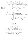
- FIG. 19 is a plan view of an FET 630 in accordance with a sixth embodiment.
- FIG. 20 is a cross-sectional view taken along the line X-X of FIG. 19 .
- FIGS. 21 and 22 show, in order of process steps, a method of manufacturing FET 630 shown in FIGS. 19 and 20 .
- FIGS. 23 and 24 show, in order of process steps, another method of manufacturing FET 630 shown in FIGS. 19 and 20 .
- an FET 30 in accordance with the first embodiment of the present invention is applied to a high voltage semiconductor device such as a high voltage switching element, and it includes a GaN epitaxial substrate 32 , a source electrode 34 , a drain electrode 36 and a gate electrode 38 .
- GaN epitaxial substrate 32 has a hetero junction structure including a buffer layer of GaN, an electron channel layer of undoped GaN, and an electron supplying layer of undoped AlGaN thinner than the electron channel layer, stacked successively on a semiconductor substrate such as a sapphire substrate. These buffer layer, electron channel layer and electron supplying layer are formed on the semiconductor substrate mentioned above, by an epitaxial growth method such as molecular beam epitaxy (MBE).
- MBE molecular beam epitaxy
- the buffer layer, the electron channel layer and the electro supplying layer have the film thickness set to 20 nm, 2 nm and 25 nm. It is noted that an epitaxial layer structure of GaN epitaxial substrate 32 is partially etched until the electron channel layer is exposed, so that an element separating mesa, not shown, is formed.
- Source electrode 34 and drain electrode 36 are spaced from each other by a prescribed distance on and in ohmic contact with the electron channel layer of the GaN epitaxial substrate 32 .
- Gate electrode 38 is in Schottky junction with the electron channel layer of epitaxial substrate 32 formed of GaN semiconductor, between source electrode 34 and drain electrode 36 .
- Gate electrode 38 has a field plate 40 at an upper portion, which protrudes like visors both to source electrode 34 and drain electrode 36 .
- the first visor portion 42 on the side of source electrode 34 of field plate 40 has its terminal end positioned closer to gate electrode 38 than an intermediate position between gate electrode 38 and source electrode 34 .
- the second visor portion 44 on the side of drain electrode 36 of field plate 40 has its terminal end positioned closer to the side of drain electrode 36 than the intermediate position between gate electrode 38 and drain electrode 36 .
- the protruding length of second visor portion 44 is set far longer than the protruding length of first visor portion 42 .
- Dielectric film 46 is formed of TaOx. In the present embodiment, as TaOx, Ta 2 O 5 is used.
- dielectric film 46 is partially removed to be flush with the terminal end surface of the first visor portion 42 , as shown by a first removed portion 48 , in a region immediately below the first visor portion 42 of field plate 40 , and it extends flat from the lower end of first removed portion 48 to source electrode 34 to be overlapped on source electrode 34 .
- dielectric film 46 is partially removed to be flush with the terminal end surface of the second visor portion 44 , as shown by a second removed portion 50 , in a region immediately below the second visor portion 44 of field plate 40 , and it extends flat from the lower end of second removed portion 50 to drain electrode 36 to be overlapped on drain electrode 36 .
- the second removed portion 50 of dielectric film 46 has its depth set such that, when a prescribed gate voltage VG is applied to gate electrode 38 and a prescribed drain voltage VD is applied to drain electrode 36 , with the voltage applied to source electrode 34 being the ground potential, electric field strength E 1 at an upper end 52 forming a boundary to the second visor portion 44 of field plate 40 and electric field strength E 2 at a lower end 54 are equal to each other.
- the depth of second removed portion 50 of dielectric film 46 has its depth set as described above, from the following reason. Specifically, if the depth of second removed portion 50 is shallower than that mentioned above, electric field strength E 1 at the upper end 52 of the second removed portion 50 exceeds the electric field strength E 2 at the lower end 54 , resulting in a breakdown of FET 30 . Similarly, if the depth of second removed portion 50 is deeper than that mentioned above, electric field strength E 2 at the lower end 54 of the second removed portion exceeds electric field strength E 1 at the upper end 52 , resulting in a breakdown of FET 30 . This is the reason why the depth of removed portion 50 is set to the thickness described above.
- the optimal depth of second removed portion 50 of dielectric film 46 should be determined in consideration of relations among dielectric constant of dielectric film 46 , film thickness of dielectric film 46 immediately below the second visor portion 44 of field plate 40 , length of the second visor portion 44 of field plate 40 , thickness of the field plate 40 and the like.
- the depth t 1 is in the range larger than 1 ⁇ 4 of film thickness t 0 and smaller than 3 ⁇ 4 of film thickness t 0 .
- the depth of first removed portion 48 of dielectric film 46 is set similar to the depth of second removed portion 50 .
- FIGS. 2 and 3 show, in the order of process steps, a method of manufacturing the FET 30 .
- preceding process steps of FIG. 2 are not shown.
- the buffer layer, the electron channel layer and the electron supplying layer are stacked successively on the semiconductor substrate by MBE, to form the epitaxial layer structure.
- the epitaxial layer structure is partially removed by etching until the electron channel layer is exposed, to form the element separating mesa described above.
- the preceding process steps are not shown.
- the step of attaining ohmic contact of source electrode 34 and drain electrode 36 , by lift-off, is performed. Specifically, first, a pattern is formed by using a resist, on GaN epitaxial substrate 32 , and on the electron channel layer of GaN epitaxial substrate 32 , a metal film formed of metal such as titanium, aluminum and molybdenum alloy is deposited. The resist pattern is removed by a resist releasing liquid, and the metal film formed on the resist film is also peeled and removed. In this manner, a metal film pattern is formed on GaN epitaxial substrate 32 at a space of resist pattern, and source electrode 34 and drain electrode 36 are formed on the electron channel layer of GaN epitaxial substrate 32 . Further, annealing is done at a prescribed temperature (in the present embodiment, 650° C.), to realize ohmic contact between substrate 32 and electrodes 34 and 36 .
- a prescribed temperature in the present embodiment, 650° C.
- dielectric film 46 of Ta 2 O 5 (for example, thickness: 350 nm) is formed on the entire surface of substrate 32 and on the structure formed on substrate 32 .
- the step of opening the gate is performed. Specifically, as shown in FIG. 2(C) , regions other than the gate forming region is masked by applying a resist 60 , and dry etching or RIE (Reactive Ion Etching) is performed. As a result, the dielectric film 46 in the gate forming region is removed by etching as shown in FIG. 2(D) , and an opening 62 is formed, through which the electron channel layer of GaN epitaxial substrate 32 is exposed. At this time point, resist 60 is removed. As to the method of removing resist 60 , ashing in O 2 plasma or a method using peeling liquid may be used. Similar method is used for removing resist in the subsequent process.
- RIE Reactive Ion Etching
- metal such as nickel and gold is successively deposited on the entire surface to fill the opening 62 , to form a gate metal film 70 , by a metal film forming technique such as vacuum vapor deposition or sputtering, as shown in FIG. 3(A) .
- the step of forming gate electrode is performed. Specifically, as shown in FIG. 3(B) , a field plate forming region is masked by applying a resist 72 , and dry etching is performed with the etching time adjusted. As a result, parts of gate metal film 70 and dielectric film 46 in the regions other than the region where the resist has been applied are removed by etching, and Schottky junction of gate electrode 38 having field plate 40 to the electron channel layer of GaN epitaxial substrate 32 is attained, as shown in FIG. 3(C) . At this time point, resist 72 is removed.
- FET 30 in accordance with the present embodiment is manufactured, as shown in FIG. 3(D) .
- a prescribed gate voltage VG is applied to gate electrode 38 and a prescribed drain voltage VD is applied to drain electrode 36 , with the voltage applied to source electrode 34 being the ground potential, and FET 30 operates thereby.
- the dielectric film 46 is partially removed as represented by a removed portion 50 , at a region immediately below the field plate 40 of gate electrode 38 , to be flush with the terminal end surface of field plate 40 .
- Dielectric film 46 extends from the lower end of removed portion 50 to the drain electrode 36 , to be overlapped on drain electrode 36 .
- the entire length of dielectric film 46 becomes longer than the field plate length, and there is no corner formed at the boundary to the terminal end of field plate 40 . Therefore, high electric field concentration at the terminal end of field plate 40 can be alleviated. As a result, it becomes possible to use FET 30 as a high voltage semiconductor device.
- an FET 230 in accordance with the second embodiment is characterized in that a recess 80 is formed at a portion of dielectric film 246 between source electrode 34 and a terminal end surface of a first visor portion 42 of field plate 40 , and at a portion between drain electrode 36 and a terminal end surface of a second visor portion 44 of field plate 40 , respectively. Except for this point, the structure is the same as that of the first embodiment.
- FET 230 is manufactured in the following manner.
- the process from the step of attaining ohmic contact of source electrode 34 and drain electrode 36 to the step of forming gate electrode 38 having field plate 40 shown in FIGS. 5(A) to 6(B) are the same as those of the first embodiment and, therefore, description of these process steps will not be repeated.
- regions other than the recess forming regions are masked by applying a resist 90 as shown in FIG. 6(C) , and dry etching is performed.
- FIG. 6(D) parts of dielectric film 246 in the recess forming regions where resist 90 is not applied are removed, and recesses 80 are formed between source electrode 34 and the terminal end surface of first visor portion 42 of field plate 40 and between drain electrode 36 and the terminal end surface of second visor portion 44 of field plate 40 .
- resist 90 is removed.
- FET 230 of the present embodiment shown in FIG. 4 is formed.
- recess 80 is formed between drain electrode 36 and the terminal end surface of field plate 40 and, therefore, electric field concentration is shifted to the side of drain electrode 36 , whereby the electric field concentration at the end portion of gate electrode 38 on the side of drain electrode 36 can effectively be dispersed and alleviated.
- Other functions and effects are the same as those of the first embodiment.
- an FET 330 in accordance with the third embodiment of the present invention is characterized in that dielectric film 346 has a two-layered structure including first and second dielectric films 100 and 102 having mutually different dielectric constants. Except for this point, the structure is the same as that of the first embodiment.
- Dielectric constant of the first dielectric film 100 as the upper layer is set to be higher than that of the second dielectric film 102 as the lower layer.
- the first dielectric film 100 is formed of TaOx
- the second dielectric film 102 is formed of SiNx.
- Ta 2 O 5 is used as the first dielectric film 100
- SiN is used as the second dielectric film 102 .
- FET 330 in accordance with the present embodiment is manufactured in the following manner.
- source electrode 34 and drain electrode 36 are formed on the electron channel layer of GaN epitaxial substrate 32 , to attain ohmic contact of these electrodes 34 and 36 .
- second dielectric film 102 (for example, film thickness: 50 nm) of SiN is formed on the electron channel layer of GaN epitaxial substrate 32 between source electrode 34 and drain electrode 36 .
- first dielectric film 100 (for example, film thickness: 150 nm) of Ta 2 O 5 is formed on the entire surface.
- regions other than the gate forming region are masked by applying a resist 110 , and dry etching or RIE is performed.
- FIG. 9(B) the first and second dielectric films 100 and 102 in the gate forming region are removed by etching, and an opening 112 is formed, through which electron channel layer of GaN epitaxial substrate 32 is exposed.
- resist 110 is removed.
- metal such as nickel and gold is successively deposited on the entire surface to fill the opening 112 by metal film forming technique such as vacuum vapor deposition or sputtering, whereby a gate metal film 114 is formed.
- a resist 120 is applied to the field plate forming region, and dry etching is performed with the etching time adjusted.
- FIG. 10 (B) parts of gate metal film 114 and first dielectric film 100 in the region other than the region where resist has been applied are removed by etching, and Schottky junction of gate electrode 38 having field plate 40 to the electron channel layer of GaN epitaxial substrate 32 is attained. At this time point, resist 120 is removed.
- FET 330 in accordance with the present embodiment shown in FIG. 7 is manufactured.
- dielectric film 346 is formed to have a two-layered structure, with the dielectric constant of the first dielectric film 100 as the upper layer set higher than that of the second dielectric film 102 as the lower layer. Therefore, the balance between collapsing and gate breakdown voltage can be improved, and even when surface state varies because of variations in the manufacturing process, good performance of FET 330 can be realized in a stable manner. Other functions and effects are the same as those of the first embodiment.
- an FET 430 in accordance with the fourth embodiment of the present invention is that at a portion of the dielectric film between source electrode 34 and the terminal end surface of first visor portion 42 of field plate 40 , and at a portion between drain electrode 36 and the terminal end surface of the second visor portion 44 of field plate 40 , recesses 130 are formed, respectively. Except for this point, the structure is the same as that of the third embodiment.
- FET 430 shown in FIG. 11 has, in place of dielectric film 346 shown in FIG. 7 , a dielectric film 446 having the two-layered structure including first and second dielectric films 400 and 402 having mutually different dielectric constants, similar to first and second dielectric films 100 and 102 of dielectric film 346 .
- FET 430 in accordance with the present embodiment is manufactured in the following manner.
- FET 430 in accordance with the present embodiment shown in FIG. 11 is formed.
- an FET 530 in accordance with the fifth embodiment of the present invention is characterized in that it has a dielectric film 546 having a two-layered structure including first and second dielectric films 500 and 502 in place of dielectric film 346 of the third embodiment, and that the second dielectric film 502 is interposed between gate electrode 38 and the electron channel layer of GaN epitaxial substrate 32 to realize MIS type structure. Except for these points, the structure is the same as that of the third embodiment.
- FET 530 in accordance with the present embodiment is manufactured in the following manner.
- source electrode 34 and drain electrode 36 are formed on the electron channel layer of GaN epitaxial substrate 32 by lift-off, and ohmic contact of these electrodes 34 and 36 are attained.
- second dielectric film 502 of SiN film is formed on the electron channel layer of GaN epitaxial substrate 32 between source electrode 34 and drain electrode 36 and, thereafter, as shown in FIG. 16(C) , by sputtering, CVD or the like, the first dielectric film 500 of Ta 2 O 5 is formed on the entire surface.
- regions other than the gate forming region are masked by applying a resist 150 , and dry etching or RIE is performed.
- the first dielectric film 500 in the gate forming region is removed by etching, and in the gate forming region, an opening 152 is formed, through which the second dielectric film 502 is exposed.
- the second dielectric film 502 serves as an etching stopper. Resist 150 is removed.
- metal such as nickel and gold is successively stacked on the entire surface to fill the opening 152 , by metal film forming technique such as vacuum vapor deposition or sputtering, to form a gate metal film 154 .
- a field plate forming region is masked by applying a resist 160 , and dry etching is performed with etching time adjusted.
- etching time adjusted As a result, as shown in FIG. 18(B) , part of gate metal film 154 and part of the first dielectric film 500 in the regions other than the region where resist has been applied are removed by etching, and Schottky junction of gate electrode 38 having field plate 40 to the electron channel layer of GaN epitaxial substrate 32 is attained. At this time point, resist 160 is removed.
- FET 530 in accordance with the present embodiment shown in FIG. 15 is manufactured.
- the second dielectric film 502 is interposed between gate electrode 38 and the electron channel layer of GaN epitaxial substrate 32 to realize MIS type structure. It is advantageous for a power transistor handling electric power, as the switching speed increases and breakdown resistance increases. Other functions and effects are the same as those of the third embodiment.
- FET 630 in accordance with the sixth embodiment of the present invention includes a drain electrode 636 having a circular shape, a gate electrode 638 arranged radially outward and spaced by a prescribed distance from drain electrode 636 and having an annular shape concentrical with drain electrode 636 , and a source electrode 634 arranged radially outward of gate electrode 638 and having an annular shape concentrical with drain electrode 636 .
- the diameter of gate electrode 638 is made smaller than the diameter of source electrode 634 .
- a field plate 170 is formed, passing above gate electrode 638 and protruding like a visor to the side of drain electrode 636 .
- Gate electrode 638 is connected through a conductor pattern 172 drawn outer than the source electrode 634 in the radial direction to a gate lead electrode 174 .
- Source electrode 634 and drain electrode 636 are in ohmic contact with GaN epitaxial substrate 32 .
- a dielectric film 646 of TaOx is formed between the electron channel layer of GaN epitaxial substrate 32 and field plate 170 .
- Ta 2 O 5 is used as TaOx.
- Dielectric film 646 is partially removed as represented by removed portion 176 in a region directly below field plate 170 to be flush with a terminal end surface of field plate 170 , and extends flat from the lower end of removed portion 176 to drain electrode 636 to be overlapped on drain electrode 636 .
- the depth of removed portion 176 of dielectric film 646 is set in the following manner. Specifically, assume that a prescribed gate voltage VG is applied to gate electrode 638 , with the voltage applied to source electrode 634 being the ground potential. At the same time, a prescribed drain voltage VD is applied to drain electrode 636 . The depth of removed portion 176 is set such that electric field strength E 1 at an upper end portion 178 forming a boundary to the terminal end of field plate 170 and electric field strength E 2 at a lower end at this time become equal to each other.
- the depth of removed portion 176 of dielectric film 646 is set as described above, from the following reason. Specifically, if the depth of removed portion 176 is shallower than the depth mentioned above, electric field strength E 1 at the upper end portion 178 of removed portion 176 exceeds electric field strength E 2 at the lower end portion 180 , resulting in breakdown of FET 630 . Similarly, if the depth of removed portion 176 is deeper than the depth mentioned above, electric field strength E 2 at the lower end portion 180 of removed portion 176 exceeds electric field strength E 1 at the upper end portion 178 , resulting in breakdown of FET 630 . Therefore, the depth of removed portion 176 is set as described above.
- the optimal depth of removed portion 176 of dielectric film 646 should be determined in consideration of relations among dielectric constant of dielectric film 646 , film thickness of dielectric film 646 immediately below field plate 170 , length of field plate 170 , thickness of field plate 170 and the like.
- the depth t 1 is set in the range larger than 1 ⁇ 4 of film thickness t 0 and smaller than 3 ⁇ 4 of film thickness t 0 .
- FET 630 in accordance with the present embodiment is manufactured in the following manner.
- source electrode 634 and drain electrode 636 are formed on the electron channel layer of GaN epitaxial substrate 32 by lift-off, and ohmic contact of these electrodes 634 and 636 are attained. Thereafter, gate electrode 638 is formed on the electron channel layer of GaN epitaxial substrate 32 .
- dielectric film 646 (for example, film thickness: 350 nm) of Ta 2 O 5 is formed.
- metal film forming technique such as vacuum vapor deposition, sputtering or the like, metal such as nickel and gold is successively stacked on the entire surface, to form a field plate metal film 190 .
- the field plate forming region is masked by applying a resist 200 , and dry etching or RIE is performed with etching time adjusted.
- etching time adjusted.
- part of field plate metal film 190 and part of dielectric film 646 in regions where resist 200 has not been applied are removed by etching, and source electrode 634 having field plate 170 is formed. At this time point, resist 200 is removed.
- FET 630 in accordance with the present embodiment shown in FIGS. 19 and 20 is manufactured.
- FET 630 of the present invention can also be manufactured by the manufacturing method shown in FIGS. 23 and 24 .
- drain electrode 636 is formed on the electron channel layer of GaN epitaxial substrate 32 by lift-off, and ohmic contact of this electrode 636 is attained. Thereafter, gate electrode 638 is formed on the electron channel layer of GaN epitaxial substrate 32 .
- dielectric film 646 (for example, film thickness: 350 nm) of Ta 2 O 5 is formed on the entire surface.
- regions other than the source forming region are masked by applying a resist 210 , and dry etching or RIE is performed to remove dielectric film 646 in the source forming region so that the electron channel layer of GaN epitaxial substrate 32 is exposed. At this time point, resist 210 is removed.
- metal film forming technique such as vacuum vapor deposition or sputtering
- metal such as nickel and gold is successively stacked on the entire surface, to form gate metal film 212 .
- the field plate forming region is masked by applying a resist 214 , and dry etching or RIE is performed with etching time adjusted.
- etching time adjusted.
- resist 214 is removed.
- a prescribed gate voltage VG is applied to gate electrode 638
- a prescribed drain voltage VD is applied to drain electrode 636 with the voltage applied to source electrode 634 being the ground potential, whereby FET 630 operates.
- gate breakdown voltage of FET 630 can be improved.
- the dielectric film 646 is removed at a region immediately below field plate 170 of source electrode 634 to be flush with the terminal end surface of field plate 170 , as represented by removed portion 176 .
- the dielectric film extends from the lower end to drain electrode 636 , to be overlapped on drain electrode 636 .
- the entire length of dielectric film 646 becomes longer than the length of field plate, and no corner is formed at the boundary between dielectric film 646 and the terminal end of field plate 170 .
- high electric field concentration can be alleviated at the terminal end of field plate 170 .
- FET 630 can be used as a high voltage semiconductor device.
- the present invention is not limited to the embodiments described above.
- the dielectric film has a single-layered structure formed of TaOx.
- the present invention is not limited to such a structure.
- the dielectric film may have a single-layered structure formed of SiNx, SiO 2 or HfOx.
- examples have been described in which the dielectric film has a two-layered structure, with the first dielectric film as the upper layer formed of TaOx and the second dielectric film as the lower layer formed of SiNx.
- the present invention is not limited to such a structure.
- the first dielectric film as the upper layer may be formed of SiNx, SiO 2 or HfOx.
- a recess may be formed between the terminal end of field plate of the source electrode and the drain electrode.
- electric field concentration is shifted to the side of drain electrode, and therefore, electric field concentration at an end portion of gate electrode on the side of drain electrode can effectively be dispersed and alleviated.
- shape of recess it is not limited to a rectangular trench, and it may be a multi-stage recess with a side wall etched stepwise.
Landscapes
- Engineering & Computer Science (AREA)
- Microelectronics & Electronic Packaging (AREA)
- Power Engineering (AREA)
- Physics & Mathematics (AREA)
- Ceramic Engineering (AREA)
- Condensed Matter Physics & Semiconductors (AREA)
- General Physics & Mathematics (AREA)
- Computer Hardware Design (AREA)
- Manufacturing & Machinery (AREA)
- Junction Field-Effect Transistors (AREA)
Applications Claiming Priority (2)
| Application Number | Priority Date | Filing Date | Title |
|---|---|---|---|
| JP2008000470A JP5134378B2 (ja) | 2008-01-07 | 2008-01-07 | 電界効果トランジスタ |
| JP2008-000470 | 2008-01-07 |
Publications (2)
| Publication Number | Publication Date |
|---|---|
| US20090206373A1 US20090206373A1 (en) | 2009-08-20 |
| US8004022B2 true US8004022B2 (en) | 2011-08-23 |
Family
ID=40954280
Family Applications (1)
| Application Number | Title | Priority Date | Filing Date |
|---|---|---|---|
| US12/348,927 Active 2029-08-01 US8004022B2 (en) | 2008-01-07 | 2009-01-06 | Field effect transistor |
Country Status (2)
| Country | Link |
|---|---|
| US (1) | US8004022B2 (ja) |
| JP (1) | JP5134378B2 (ja) |
Cited By (3)
| Publication number | Priority date | Publication date | Assignee | Title |
|---|---|---|---|---|
| US20130228788A1 (en) * | 2012-03-01 | 2013-09-05 | Kabushiki Kaisha Toshiba | Semiconductor device |
| US20130228789A1 (en) * | 2012-03-02 | 2013-09-05 | Kabushiki Kaisha Toshiba | Semiconductor device |
| US20140264588A1 (en) * | 2013-03-14 | 2014-09-18 | Taiwan Semiconductor Manufacturing Co. Ltd. | Metal Oxide Semiconductor Field-Effect Transistor (MOSFET) with Step Oxide |
Families Citing this family (14)
| Publication number | Priority date | Publication date | Assignee | Title |
|---|---|---|---|---|
| KR101118268B1 (ko) * | 2009-08-27 | 2012-03-20 | 한국산업기술대학교산학협력단 | 요철 패턴 기판 상의 고품질 비극성/반극성 반도체 소자 및 그 제조 방법 |
| JP2011142182A (ja) * | 2010-01-06 | 2011-07-21 | Sharp Corp | 電界効果トランジスタ |
| JP2011204780A (ja) * | 2010-03-24 | 2011-10-13 | Toshiba Corp | 半導体装置 |
| JP5691267B2 (ja) * | 2010-07-06 | 2015-04-01 | サンケン電気株式会社 | 半導体装置 |
| KR101652403B1 (ko) * | 2010-08-13 | 2016-08-31 | 삼성전자주식회사 | 전력 전자소자 및 그 제조방법 |
| JP6085442B2 (ja) * | 2012-09-28 | 2017-02-22 | トランスフォーム・ジャパン株式会社 | 化合物半導体装置及びその製造方法 |
| US20140319586A1 (en) | 2013-04-26 | 2014-10-30 | Raytheon Company | Photolithographic, thickness non-uniformity, compensation features for optical photolithographic semiconductor structure formation |
| JP2015056457A (ja) | 2013-09-10 | 2015-03-23 | 株式会社東芝 | 半導体装置 |
| CN103762234B (zh) * | 2014-01-22 | 2016-03-02 | 西安电子科技大学 | 基于超结漏场板的AlGaN/GaN MISHEMT高压器件及其制作方法 |
| CN103779411B (zh) * | 2014-01-22 | 2017-01-25 | 西安电子科技大学 | 基于超结槽栅的高压器件及其制作方法 |
| CN103779410B (zh) * | 2014-01-22 | 2018-02-27 | 西安电子科技大学 | 基于超结漏场板的槽栅高压器件及其制作方法 |
| US20190097001A1 (en) * | 2017-09-25 | 2019-03-28 | Raytheon Company | Electrode structure for field effect transistor |
| US10720497B2 (en) * | 2017-10-24 | 2020-07-21 | Raytheon Company | Transistor having low capacitance field plate structure |
| CN112864015B (zh) * | 2021-01-27 | 2022-07-05 | 浙江集迈科微电子有限公司 | GaN器件及制备方法 |
Citations (12)
| Publication number | Priority date | Publication date | Assignee | Title |
|---|---|---|---|---|
| JP2000003919A (ja) | 1998-06-16 | 2000-01-07 | Nec Corp | 電界効果型トランジスタ |
| JP2000100831A (ja) | 1998-09-22 | 2000-04-07 | Nec Corp | 電界効果型トランジスタ |
| JP2001230263A (ja) | 2001-01-29 | 2001-08-24 | Nec Corp | 電界効果型トランジスタ |
| JP2001237250A (ja) | 2000-02-22 | 2001-08-31 | Nec Corp | 半導体装置 |
| US6586813B2 (en) * | 2000-07-17 | 2003-07-01 | Fujitsu Quantum Devices Limited | High-speed compound semiconductor device operable at large output power with minimum leakage current |
| US20030132463A1 (en) * | 2002-01-08 | 2003-07-17 | Yosuke Miyoshi | Schottky gate field effect transistor |
| JP2004200248A (ja) | 2002-12-16 | 2004-07-15 | Nec Corp | 電界効果トランジスタ |
| US20050189559A1 (en) | 2004-02-27 | 2005-09-01 | Kabushiki Kaisha Toshiba | Semiconductor device |
| US7180103B2 (en) * | 2004-09-24 | 2007-02-20 | Agere Systems Inc. | III-V power field effect transistors |
| JP2007250950A (ja) | 2006-03-17 | 2007-09-27 | Nippon Telegr & Teleph Corp <Ntt> | 窒化物半導体を用いたヘテロ構造電界効果トランジスタ |
| US20070235761A1 (en) * | 2003-09-09 | 2007-10-11 | Cree, Inc. | Wide bandgap transistor devices with field plates |
| US20090200576A1 (en) * | 2008-02-13 | 2009-08-13 | Kabushiki Kaisha Toshiba | Semiconductor device |
Family Cites Families (3)
| Publication number | Priority date | Publication date | Assignee | Title |
|---|---|---|---|---|
| JP2006086398A (ja) * | 2004-09-17 | 2006-03-30 | Matsushita Electric Ind Co Ltd | 半導体装置及びその製造方法 |
| JP5065616B2 (ja) * | 2006-04-21 | 2012-11-07 | 株式会社東芝 | 窒化物半導体素子 |
| US7711212B2 (en) * | 2007-09-21 | 2010-05-04 | International Business Machines Corporation | Junction field effect transistor geometry for optical modulators |
-
2008
- 2008-01-07 JP JP2008000470A patent/JP5134378B2/ja active Active
-
2009
- 2009-01-06 US US12/348,927 patent/US8004022B2/en active Active
Patent Citations (18)
| Publication number | Priority date | Publication date | Assignee | Title |
|---|---|---|---|---|
| JP2000003919A (ja) | 1998-06-16 | 2000-01-07 | Nec Corp | 電界効果型トランジスタ |
| US6100571A (en) | 1998-06-16 | 2000-08-08 | Nec Corporation | Fet having non-overlapping field control electrode between gate and drain |
| JP2000100831A (ja) | 1998-09-22 | 2000-04-07 | Nec Corp | 電界効果型トランジスタ |
| US6483135B1 (en) * | 1998-09-22 | 2002-11-19 | Nec Compound Semiconductor Devices, Ltd. | Field effect transistor |
| US20030006437A1 (en) | 1998-09-22 | 2003-01-09 | Nec Corporation | Field effect transistor |
| JP2001237250A (ja) | 2000-02-22 | 2001-08-31 | Nec Corp | 半導体装置 |
| US6586813B2 (en) * | 2000-07-17 | 2003-07-01 | Fujitsu Quantum Devices Limited | High-speed compound semiconductor device operable at large output power with minimum leakage current |
| JP2001230263A (ja) | 2001-01-29 | 2001-08-24 | Nec Corp | 電界効果型トランジスタ |
| US20030132463A1 (en) * | 2002-01-08 | 2003-07-17 | Yosuke Miyoshi | Schottky gate field effect transistor |
| JP2004200248A (ja) | 2002-12-16 | 2004-07-15 | Nec Corp | 電界効果トランジスタ |
| US20060102929A1 (en) * | 2002-12-16 | 2006-05-18 | Yasuhiro Okamoto | Field-effect transistor |
| US20070235761A1 (en) * | 2003-09-09 | 2007-10-11 | Cree, Inc. | Wide bandgap transistor devices with field plates |
| US20050189559A1 (en) | 2004-02-27 | 2005-09-01 | Kabushiki Kaisha Toshiba | Semiconductor device |
| JP2005244072A (ja) | 2004-02-27 | 2005-09-08 | Toshiba Corp | 半導体装置 |
| US20060138454A1 (en) | 2004-02-27 | 2006-06-29 | Kabushiki Kaisha Toshiba | Semiconductor device using a nitride semiconductor |
| US7180103B2 (en) * | 2004-09-24 | 2007-02-20 | Agere Systems Inc. | III-V power field effect transistors |
| JP2007250950A (ja) | 2006-03-17 | 2007-09-27 | Nippon Telegr & Teleph Corp <Ntt> | 窒化物半導体を用いたヘテロ構造電界効果トランジスタ |
| US20090200576A1 (en) * | 2008-02-13 | 2009-08-13 | Kabushiki Kaisha Toshiba | Semiconductor device |
Cited By (4)
| Publication number | Priority date | Publication date | Assignee | Title |
|---|---|---|---|---|
| US20130228788A1 (en) * | 2012-03-01 | 2013-09-05 | Kabushiki Kaisha Toshiba | Semiconductor device |
| US20130228789A1 (en) * | 2012-03-02 | 2013-09-05 | Kabushiki Kaisha Toshiba | Semiconductor device |
| US8890263B2 (en) * | 2012-03-02 | 2014-11-18 | Kabushiki Kaisha Toshiba | Semiconductor device |
| US20140264588A1 (en) * | 2013-03-14 | 2014-09-18 | Taiwan Semiconductor Manufacturing Co. Ltd. | Metal Oxide Semiconductor Field-Effect Transistor (MOSFET) with Step Oxide |
Also Published As
| Publication number | Publication date |
|---|---|
| JP5134378B2 (ja) | 2013-01-30 |
| US20090206373A1 (en) | 2009-08-20 |
| JP2009164339A (ja) | 2009-07-23 |
Similar Documents
| Publication | Publication Date | Title |
|---|---|---|
| US8004022B2 (en) | Field effect transistor | |
| KR101992565B1 (ko) | 고 전자이동도 트랜지스터 및 그 제조 방법 | |
| US9831315B2 (en) | Semiconductor devices with field plates | |
| EP2080228B1 (en) | Single voltage supply pseudomorphic high electron mobility transistor (phemt) power device and process for manufacturing the same | |
| US8193561B2 (en) | Semiconductor device and method of manufacturing the same | |
| EP2840593B1 (en) | Enhanced switch device and manufacturing method therefor | |
| US10096702B2 (en) | Multi-step surface passivation structures and methods for fabricating same | |
| US8278688B2 (en) | Compound semiconductor device and manufacturing method thereof | |
| JP2018107462A (ja) | 半導体デバイスおよびその製造方法 | |
| JP2008112868A (ja) | 半導体装置およびその製造方法 | |
| US10840353B2 (en) | High electron mobility transistor with dual thickness barrier layer | |
| US20120280281A1 (en) | Gallium nitride or other group iii/v-based schottky diodes with improved operating characteristics | |
| US10134854B2 (en) | High electron mobility transistor and fabrication method thereof | |
| JP5596636B2 (ja) | 電界効果トランジスタ | |
| JP2012004573A (ja) | 電界効果トランジスタ | |
| CN113410285B (zh) | 半导体器件及其制备方法 | |
| US20230282727A1 (en) | Hemt device and manufacturing process thereof | |
| US20240154012A1 (en) | Semiconductor device and method for manufacturing the same | |
| JP2017208379A (ja) | 窒化物半導体装置 | |
| CN117293166A (zh) | 半导体器件及其制备方法 | |
| JP2018037567A (ja) | 半導体装置の製造方法、及び半導体装置 |
Legal Events
| Date | Code | Title | Description |
|---|---|---|---|
| AS | Assignment |
Owner name: SHARP KABUSHIKI KAISHA, JAPAN Free format text: ASSIGNMENT OF ASSIGNORS INTEREST;ASSIGNORS:YAFUNE, NORIMASA;TWYNAM, JOHN KEVIN;REEL/FRAME:022596/0898;SIGNING DATES FROM 20090216 TO 20090223 Owner name: SHARP KABUSHIKI KAISHA, JAPAN Free format text: ASSIGNMENT OF ASSIGNORS INTEREST;ASSIGNORS:YAFUNE, NORIMASA;TWYNAM, JOHN KEVIN;SIGNING DATES FROM 20090216 TO 20090223;REEL/FRAME:022596/0898 |
|
| STCF | Information on status: patent grant |
Free format text: PATENTED CASE |
|
| FEPP | Fee payment procedure |
Free format text: PAYOR NUMBER ASSIGNED (ORIGINAL EVENT CODE: ASPN); ENTITY STATUS OF PATENT OWNER: LARGE ENTITY |
|
| FEPP | Fee payment procedure |
Free format text: PAYER NUMBER DE-ASSIGNED (ORIGINAL EVENT CODE: RMPN); ENTITY STATUS OF PATENT OWNER: LARGE ENTITY Free format text: PAYOR NUMBER ASSIGNED (ORIGINAL EVENT CODE: ASPN); ENTITY STATUS OF PATENT OWNER: LARGE ENTITY |
|
| FPAY | Fee payment |
Year of fee payment: 4 |
|
| MAFP | Maintenance fee payment |
Free format text: PAYMENT OF MAINTENANCE FEE, 8TH YEAR, LARGE ENTITY (ORIGINAL EVENT CODE: M1552); ENTITY STATUS OF PATENT OWNER: LARGE ENTITY Year of fee payment: 8 |
|
| AS | Assignment |
Owner name: MURATA MANUFACTURING CO., LTD., JAPAN Free format text: ASSIGNMENT OF ASSIGNORS INTEREST;ASSIGNOR:SHARP KABUSHIKI KAISHA;REEL/FRAME:049403/0835 Effective date: 20190530 |
|
| MAFP | Maintenance fee payment |
Free format text: PAYMENT OF MAINTENANCE FEE, 12TH YEAR, LARGE ENTITY (ORIGINAL EVENT CODE: M1553); ENTITY STATUS OF PATENT OWNER: LARGE ENTITY Year of fee payment: 12 |