US7705486B2 - Integrated circuit having multiple power domains - Google Patents
Integrated circuit having multiple power domains Download PDFInfo
- Publication number
- US7705486B2 US7705486B2 US11/707,500 US70750007A US7705486B2 US 7705486 B2 US7705486 B2 US 7705486B2 US 70750007 A US70750007 A US 70750007A US 7705486 B2 US7705486 B2 US 7705486B2
- Authority
- US
- United States
- Prior art keywords
- power
- integrated circuit
- operating mode
- power line
- predetermined operating
- Prior art date
- Legal status (The legal status is an assumption and is not a legal conclusion. Google has not performed a legal analysis and makes no representation as to the accuracy of the status listed.)
- Active, expires
Links
Images


Classifications
-
- G—PHYSICS
- G06—COMPUTING OR CALCULATING; COUNTING
- G06F—ELECTRIC DIGITAL DATA PROCESSING
- G06F1/00—Details not covered by groups G06F3/00 - G06F13/00 and G06F21/00
- G06F1/26—Power supply means, e.g. regulation thereof
- G06F1/32—Means for saving power
- G06F1/3203—Power management, i.e. event-based initiation of a power-saving mode
-
- F—MECHANICAL ENGINEERING; LIGHTING; HEATING; WEAPONS; BLASTING
- F25—REFRIGERATION OR COOLING; COMBINED HEATING AND REFRIGERATION SYSTEMS; HEAT PUMP SYSTEMS; MANUFACTURE OR STORAGE OF ICE; LIQUEFACTION SOLIDIFICATION OF GASES
- F25D—REFRIGERATORS; COLD ROOMS; ICE-BOXES; COOLING OR FREEZING APPARATUS NOT OTHERWISE PROVIDED FOR
- F25D11/00—Self-contained movable devices, e.g. domestic refrigerators
- F25D11/02—Self-contained movable devices, e.g. domestic refrigerators with cooling compartments at different temperatures
-
- F—MECHANICAL ENGINEERING; LIGHTING; HEATING; WEAPONS; BLASTING
- F25—REFRIGERATION OR COOLING; COMBINED HEATING AND REFRIGERATION SYSTEMS; HEAT PUMP SYSTEMS; MANUFACTURE OR STORAGE OF ICE; LIQUEFACTION SOLIDIFICATION OF GASES
- F25D—REFRIGERATORS; COLD ROOMS; ICE-BOXES; COOLING OR FREEZING APPARATUS NOT OTHERWISE PROVIDED FOR
- F25D17/00—Arrangements for circulating cooling fluids; Arrangements for circulating gas, e.g. air, within refrigerated spaces
- F25D17/04—Arrangements for circulating cooling fluids; Arrangements for circulating gas, e.g. air, within refrigerated spaces for circulating air, e.g. by convection
- F25D17/06—Arrangements for circulating cooling fluids; Arrangements for circulating gas, e.g. air, within refrigerated spaces for circulating air, e.g. by convection by forced circulation
- F25D17/067—Evaporator fan units
-
- F—MECHANICAL ENGINEERING; LIGHTING; HEATING; WEAPONS; BLASTING
- F25—REFRIGERATION OR COOLING; COMBINED HEATING AND REFRIGERATION SYSTEMS; HEAT PUMP SYSTEMS; MANUFACTURE OR STORAGE OF ICE; LIQUEFACTION SOLIDIFICATION OF GASES
- F25D—REFRIGERATORS; COLD ROOMS; ICE-BOXES; COOLING OR FREEZING APPARATUS NOT OTHERWISE PROVIDED FOR
- F25D25/00—Charging, supporting, and discharging the articles to be cooled
- F25D25/02—Charging, supporting, and discharging the articles to be cooled by shelves
- F25D25/028—Cooled supporting means
-
- G—PHYSICS
- G06—COMPUTING OR CALCULATING; COUNTING
- G06F—ELECTRIC DIGITAL DATA PROCESSING
- G06F1/00—Details not covered by groups G06F3/00 - G06F13/00 and G06F21/00
- G06F1/26—Power supply means, e.g. regulation thereof
- G06F1/32—Means for saving power
- G06F1/3203—Power management, i.e. event-based initiation of a power-saving mode
- G06F1/3234—Power saving characterised by the action undertaken
- G06F1/3243—Power saving in microcontroller unit
-
- G—PHYSICS
- G06—COMPUTING OR CALCULATING; COUNTING
- G06F—ELECTRIC DIGITAL DATA PROCESSING
- G06F1/00—Details not covered by groups G06F3/00 - G06F13/00 and G06F21/00
- G06F1/26—Power supply means, e.g. regulation thereof
- G06F1/32—Means for saving power
- G06F1/3203—Power management, i.e. event-based initiation of a power-saving mode
- G06F1/3234—Power saving characterised by the action undertaken
- G06F1/3296—Power saving characterised by the action undertaken by lowering the supply or operating voltage
-
- F—MECHANICAL ENGINEERING; LIGHTING; HEATING; WEAPONS; BLASTING
- F25—REFRIGERATION OR COOLING; COMBINED HEATING AND REFRIGERATION SYSTEMS; HEAT PUMP SYSTEMS; MANUFACTURE OR STORAGE OF ICE; LIQUEFACTION SOLIDIFICATION OF GASES
- F25D—REFRIGERATORS; COLD ROOMS; ICE-BOXES; COOLING OR FREEZING APPARATUS NOT OTHERWISE PROVIDED FOR
- F25D2400/00—General features of, or devices for refrigerators, cold rooms, ice-boxes, or for cooling or freezing apparatus not covered by any other subclass
- F25D2400/28—Quick cooling
-
- Y—GENERAL TAGGING OF NEW TECHNOLOGICAL DEVELOPMENTS; GENERAL TAGGING OF CROSS-SECTIONAL TECHNOLOGIES SPANNING OVER SEVERAL SECTIONS OF THE IPC; TECHNICAL SUBJECTS COVERED BY FORMER USPC CROSS-REFERENCE ART COLLECTIONS [XRACs] AND DIGESTS
- Y02—TECHNOLOGIES OR APPLICATIONS FOR MITIGATION OR ADAPTATION AGAINST CLIMATE CHANGE
- Y02D—CLIMATE CHANGE MITIGATION TECHNOLOGIES IN INFORMATION AND COMMUNICATION TECHNOLOGIES [ICT], I.E. INFORMATION AND COMMUNICATION TECHNOLOGIES AIMING AT THE REDUCTION OF THEIR OWN ENERGY USE
- Y02D10/00—Energy efficient computing, e.g. low power processors, power management or thermal management
Definitions
- the present invention relates generally to integrated circuits, and more particularly, to an integrated circuit having multiple power domains with power lines that are connected together in a predetermined operating mode.
- a semiconductor integrated circuit fabricated as a conventional flash memory has generally used a power voltage of 5 Volts as an operating voltage.
- lower operating voltages are desired with higher integration and scaling-down of semiconductor integration circuits.
- an operating voltage of about 1.0 V is used for a memory device, and an operating voltage of from about 0.6 Volts to about 1.3 Volts is used for a logic circuit such as a central processing unit (CPU) depending on an operating mode thereof.
- CPU central processing unit
- multi-power domain technology is used for separating power domains among different functional blocks with control of turning on/off the power supplied to the multiple power domains depending on operating modes of the functional blocks.
- FIG. 1 is a block diagram of a semiconductor integrated circuit 10 according to the conventional art.
- the integrated circuit 10 includes a regulator 11 for generating internal operating voltages and two power domains 13 and 15 . Each of the power domains 13 and 15 independently receives a respective voltage from the regulator 11 .
- the power domain 13 receives a first operating voltage V from the regulator 11
- the power domain 11 receives a second operating voltage V′ from the regulator 11
- the first and second operating voltages V and V′ may each be set to a same voltage level or to different voltage levels, as disclosed in U.S. Pat. No. 6,650,589.
- power lines of the power domains 13 and 15 in the prior art remain separated (i.e., disconnected) from each-other.
- the IR voltage drops in the separated power domains 13 and 15 may be higher and more difficult to control than when the integrated circuit has one power domain.
- the IR voltage drop within one of the power domains 13 and 15 may become high enough for significantly degrading the operating frequency of the integrated circuit. Nevertheless, multiple power domains for an integrated circuit are desired for minimizing power consumption.
- an integrated circuit according to the present invention is implemented with multiple power domains with a mechanism for separating and coupling the multiple power domains depending on the operating mode of the integrated circuit.
- An integrated circuit includes first and second power domains, a power supply control unit, and a switch block.
- the power supply control unit supplies a first voltage to the first power domain and a second voltage to the second power domain.
- the switch block provides at least one current path between the first and second power domains during a predetermined operating mode.
- the switch block diverts current to the second power domain from the first power domain for increasing the total current in the second power domain during the predetermined operating mode.
- the integrated circuit further includes a first power line having the first voltage applied thereon within the first power domain, and a second power line having the second voltage applied thereon within the second power domain.
- the switch block connects the first power line to the second power line during the predetermined operating mode.
- the first and second voltages are set to a same voltage level during the predetermined operating mode.
- the switch block disconnects the first power line from the second power line when the integrated circuit is not in the predetermined operating mode.
- the first and second voltages are set to different voltage levels when the integrated circuit is not in the predetermined operating mode.
- the switch block includes a plurality of transistors, with each transistor being turned on for providing a respective current path between the first and second power domains during the predetermined operating mode.
- the integrated circuit further includes a third power domain and another switch block.
- the power supply control unit supplies a third voltage to the third power domain
- the other switch block provides at least one current path between the third and second power domains during the predetermined operating mode.
- the switch block connects the third power line to the second power line during the predetermined operating mode.
- the first, second, and third voltages are set to a same voltage level during the predetermined operating mode.
- the first power line is formed as a first power mesh within the first power domain
- the second power line is formed as a second power mesh within the second power domain.
- the switch block includes a plurality of transistors that are turned on for connecting the first power line to the second power line during the predetermined operating mode.
- the first and second power domains are separated for minimizing power consumption when the integrated circuit does not operate in the predetermined operating mode.
- the first and second power domains are connected for more flexible control of current flow therein during the predetermined operating mode when high frequency operation is more critical.
- FIG. 1 is a block diagram of a semiconductor integrated circuit with multiple power domains according to the conventional art
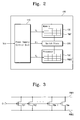
- FIG. 2 is a block diagram of a semiconductor integrated circuit with multiple power domains, according to an embodiment of the present invention
- FIG. 3 is a circuit diagram of a switch block in FIG. 2 , according to an embodiment of the present invention.
- FIG. 4 is a block diagram of a semiconductor integrated circuit with multiple power domains, according to another embodiment of the present invention.
- FIGS. 1 , 2 , 3 , and 4 refer to elements having similar structure and/or function.
- FIG. 2 is a block diagram of a semiconductor integrated circuit 100 according to an embodiment of the present invention.
- the integrated circuit 100 includes a power supply control unit 110 , a memory unit 130 , a processor 150 , and a switch block 200 .
- the memory unit 130 and the processor 150 are implemented as separate power domains that are physically separated. That is, the power domains 130 and 150 have separate physical power supply lines for receiving respective operating voltages applied thereon.
- the power supply control unit 110 provides respective operating voltages V 1 and V 2 to the multiple power domains 130 and 150 .
- the power supply control unit 110 may be fabricated as part of the integrated circuit 100 or may be formed outside the integrated circuit 100 . If formed outside the integrated circuit 100 , the integrated circuit 100 has separate pins receiving the operating voltages V 1 and V 2 from the external power supply control unit 110 .
- the power supply control unit 110 that is formed as part of the integrated circuit 100 uses an externally provided power voltage Vcc to generate internal power (i.e., operating) voltages V 1 and V 2 to the memory unit 130 and the processor 150 , respectively.
- the power supply control unit 110 supplies a first operating voltage V 1 to the first power domain 130 and supplies a second operating voltage V 2 to the second power domain 150 .
- the memory unit 130 as the first power domain includes a first power line PWR 1 implemented as a first power mesh having a network structure of meshes according to an example embodiment of the present invention.
- the processor 130 as the second power domain includes a second power line PWR 2 implemented as a second power mesh having a network structure of meshes according to an example embodiment of the present invention.
- the first operating voltage V 1 is applied on the first power line PWR 1 of the first power domain 130
- the second operating voltage V 2 is applied on the second power line PWR 2 of the second power domain 150
- the operating voltages V 1 and V 2 are set to the same voltage level or are set to different voltage levels depending on the operating mode of the integrated circuit 100 .
- the operating voltage V 2 supplied to the processor 150 is about 0.7 V (Volt) or less, while the operating voltage V 1 supplied to the memory unit 130 is in a range of from about 1.0 V to about 1.3 V, during a power save mode of the integrated circuit 100 .
- the first and second operating voltages V 1 and V 2 during a normal operating mode of the integrated circuit 100 are set to a same voltage level of 1.0 V.
- the second operating voltage V 2 supplied to the processor 150 is turned off for reducing power consumption, and the first operating voltage V 1 supplied to the memory unit 130 is set to about 1.0 V for minimizing wake-up time of the integrated circuit 100 .
- the memory unit 130 and the processor 150 are formed as separate power domains for separate control of the operating voltages V 1 and V 2 such that operating stability of the memory device 130 is maintained while simultaneously reducing power consumption of the processor 150 .
- the memory device 130 and the processor 150 were formed as one power domain receiving one operating voltage via one power line, such an operating voltage is limited by the memory device 130 . That is, the memory device 130 cannot operate properly under a predetermined voltage (e.g., about 1.0 V). However, logic circuits inside the processor 150 generally operate well even at a low voltage (about 0.7 V). Thus, the operating voltage to the processor 150 is lowered to such a low voltage level during a power save mode when the integrated circuit 100 does not need to operate at a maximum operating frequency.
- a predetermined voltage e.g., about 1.0 V
- logic circuits inside the processor 150 generally operate well even at a low voltage (about 0.7 V).
- the operating voltage to the processor 150 is lowered to such a low voltage level during a power save mode when the integrated circuit 100 does not need to operate at a maximum operating frequency.
- the memory device 130 and the processor 150 were to receive just one operating voltage, the higher operating voltage (of about 1.0 V) is also applied on the processor 150 increasing power consumption even during the power save mode.
- the memory 130 and the processor 150 are formed as separate power domains having separate power lines such that respective operating voltage V 1 and V 2 thereto may be independently controlled depending on the operating mode of the integrated circuit 100 .
- the power supply control unit 110 regulates an external power voltage Vcc to generate the first and second operating voltages V 1 and V 2 set to a same voltage level in a range of from about 1.0 V to about 1.3 V during the normal operating mode when the operating frequency of the processor 150 is more critical.
- the power supply control unit 110 sets the first operating voltage V 1 supplied to the memory 130 at about 1.0 V, but sets the second operating voltage V 2 supplied to the processor 150 to a lower voltage of about 0.7 V during a power save mode where the operating frequency of the integrated circuit 100 is not as critical.
- power consumption of the integrated circuit 100 may be minimized during the power save mode.
- IR current resistance
- the present invention reduces the IR voltage drops in the processor 150 during such a normal operating mode.
- the integrated circuit 100 includes the switch block 200 that is controlled by the power supply control unit 110 .
- the switch block 200 includes a plurality of PMOSFETs (P-channel metal oxide semiconductor field effect transistors) PM 1 , PM 2 , . . . , and PMm.
- PMOSFETs P-channel metal oxide semiconductor field effect transistors
- Each of the PMOSFETs PM 1 , PM 2 , . . . , and PMm has a respective drain and source coupled between the first and second power lines PWR 1 and PWR 2 .
- the gates of the PMOSFETs PM 1 , PM 2 , . . . , and PMm have an enable control signal En applied thereon.
- the enable control signal En is generated by the power supply control unit 110 .
- the enable control signal En is activated by the power supply control unit 110 to turn on each of the PMOSFETs PM 1 , PM 2 , . . . , and PMm of the switch block 200 .
- the PMOSFETs PM 1 , PM 2 , . . . , and PMm that are turned on connect the first power line PWR 1 of the first power domain 130 to the second power line PWR 2 of the second power domain 150 , during the normal operating mode of the integrated circuit 100 .
- the enable control signal En is deactivated by the power supply control unit 110 to turn off each of the PMOSFETs PM 1 , PM 2 , . . . , and PMm when the integrated circuit is not operating in the normal operating mode. In that case such as during the power save mode, the first power line PWR 1 of the first power domain 130 remains disconnected from the second power line PWR 2 of the second power domain 150 when the voltages applied on the power lines PWR 1 and PWR 2 are set to different voltage levels.
- each of the PMOSFETs PM 1 , PM 2 , . . . , and PMm forms a respective current path for diverting respective current to the processor 150 from the memory unit 130 .
- current diverted to the processor 150 from the memory unit 130 may be originated in the power supply control unit 110 .
- Such an increase of current to the processor 150 may decrease resistances in the processor 150 for reducing IR voltage drops in the processor 150 during the normal operating mode.
- the reduced IR voltage drops improve the operating frequency of the integrated circuit 100 .
- the increased current itself to the processor 150 also enhances the operating frequency of the processor 150 during the normal operating mode.
- the integrated circuit 100 is restored to the normal operating mode from the power save mode during a reset or a power-up.
- the power supply control unit 110 sets the first and second operating voltages V 1 and V 2 to a same voltage level such as about 1.0 V.
- the power supply control unit 110 raises the second operating voltage V 2 applied on the second power line PWR 2 from about 0.7 V to about 1.0 V which is same as the first operating voltage V 1 .
- the power supply control unit 110 activates the enable control signal En for turning on the PMOSFETs PM 1 , PM 2 , . . . , and PMm for connecting the first and second power meshes PWR 1 and PWR 2 of the memory device 130 and the processor 150 .
- FIG. 4 is a block diagram of a semiconductor integrated circuit 200 according to another embodiment of the present invention. Elements having the same reference number in FIGS. 2 and 4 refer to elements having similar structure and/or function. However, the integrated circuit 200 of FIG. 4 further includes a peripheral circuit 170 forming a third power domain and another switch block 210 .
- the third power domain 170 has a third power line PWR 3 which may be implemented as a third power mesh PWR 3 having a network structure of meshes.
- the power supply control unit 110 supplies a third operating voltage V 3 applied on the third power line PWR 3 of the third power domain 170 .
- the switch block 210 is implemented similarly as illustrated in FIG. 3 with multiple PMOSFETs between the processor 150 and the peripheral circuit 170 .
- Such PMOSFETs in the switch block 210 have gates with the enable control signal En applied thereon by the power supply control unit 110 similar to the switch block 200 .
- the PMOSFETs in the switch blocks 200 and 210 are turned on.
- the first power line PWR 1 is connected to the second power line PWR 2 via the switch block 200
- the third power line PWR 3 is connected to the second power lien PWR 2 via the switch block 210 .
- current paths are formed between the first and second power domains 130 and 150 and between the second and third power domains 150 and 170 , during the normal operating mode of the integrated circuit 200 .
- the operating voltages V 1 , V 2 , and V 3 to the power domains 130 , 150 , and 170 , respectively are set to different voltage levels since the processor 150 does not need to operate at maximum operating frequency.
- the PMOSFETs in the switch blocks 200 and 210 are turned off such that the power lines PWR 1 , PWR 2 , and PWR 3 of the power domains 130 , 150 , and 170 , respectively, remain disconnected from each other.
- the third operating voltage V 3 to the peripheral circuit 170 is set to a higher voltage than the second operating voltage V 2 or may be turned off.
- the peripheral circuit 170 may include an analog-to-digital converter (ADC).
- ADC analog-to-digital converter
- the present invention may also be practiced with the memory unit 130 being a flash memory device and with a dynamic random access memory (DRAM) being used instead of the peripheral circuit 170 .
- DRAM dynamic random access memory
- power consumption may be minimized during one operating mode while operating frequency is enhanced during another operating mode.
Landscapes
- Engineering & Computer Science (AREA)
- Theoretical Computer Science (AREA)
- Physics & Mathematics (AREA)
- General Engineering & Computer Science (AREA)
- General Physics & Mathematics (AREA)
- Chemical & Material Sciences (AREA)
- Combustion & Propulsion (AREA)
- Mechanical Engineering (AREA)
- Thermal Sciences (AREA)
- Semiconductor Integrated Circuits (AREA)
Applications Claiming Priority (2)
| Application Number | Priority Date | Filing Date | Title |
|---|---|---|---|
| KR1020060019485A KR101229508B1 (ko) | 2006-02-28 | 2006-02-28 | 복수의 파워도메인을 포함하는 반도체 집적 회로 |
| KR2006-19485 | 2006-02-28 |
Publications (2)
| Publication Number | Publication Date |
|---|---|
| US20070234083A1 US20070234083A1 (en) | 2007-10-04 |
| US7705486B2 true US7705486B2 (en) | 2010-04-27 |
Family
ID=38560895
Family Applications (1)
| Application Number | Title | Priority Date | Filing Date |
|---|---|---|---|
| US11/707,500 Active 2027-11-20 US7705486B2 (en) | 2006-02-28 | 2007-02-16 | Integrated circuit having multiple power domains |
Country Status (3)
| Country | Link |
|---|---|
| US (1) | US7705486B2 (ko) |
| KR (1) | KR101229508B1 (ko) |
| TW (1) | TWI342026B (ko) |
Cited By (2)
| Publication number | Priority date | Publication date | Assignee | Title |
|---|---|---|---|---|
| US9134777B2 (en) | 2012-06-06 | 2015-09-15 | Qualcomm Incorporated | Bi-modal power delivery scheme for an integrated circuit comprising multiple functional blocks on a single die to achieve desired average throughput for the integrated circuit |
| US10324521B2 (en) | 2012-10-17 | 2019-06-18 | Semiconductor Energy Laboratory Co., Ltd. | Microcontroller and method for manufacturing the same |
Families Citing this family (22)
| Publication number | Priority date | Publication date | Assignee | Title |
|---|---|---|---|---|
| JP5315617B2 (ja) * | 2007-02-21 | 2013-10-16 | 富士通セミコンダクター株式会社 | 多電源制御方法及び半導体集積回路 |
| JP4960813B2 (ja) * | 2007-09-14 | 2012-06-27 | 株式会社リコー | 電力制御システム |
| US8171323B2 (en) * | 2008-07-01 | 2012-05-01 | Broadcom Corporation | Integrated circuit with modular dynamic power optimization architecture |
| GB2472050B (en) * | 2009-07-22 | 2013-06-19 | Wolfson Microelectronics Plc | Power management apparatus and methods |
| US8769316B2 (en) | 2011-09-06 | 2014-07-01 | Intel Corporation | Dynamically allocating a power budget over multiple domains of a processor |
| US9074947B2 (en) | 2011-09-28 | 2015-07-07 | Intel Corporation | Estimating temperature of a processor core in a low power state without thermal sensor information |
| US8954770B2 (en) * | 2011-09-28 | 2015-02-10 | Intel Corporation | Controlling temperature of multiple domains of a multi-domain processor using a cross domain margin |
| US8832478B2 (en) | 2011-10-27 | 2014-09-09 | Intel Corporation | Enabling a non-core domain to control memory bandwidth in a processor |
| US9026815B2 (en) | 2011-10-27 | 2015-05-05 | Intel Corporation | Controlling operating frequency of a core domain via a non-core domain of a multi-domain processor |
| US8943340B2 (en) | 2011-10-31 | 2015-01-27 | Intel Corporation | Controlling a turbo mode frequency of a processor |
| US9158693B2 (en) | 2011-10-31 | 2015-10-13 | Intel Corporation | Dynamically controlling cache size to maximize energy efficiency |
| CN103197933A (zh) * | 2012-01-06 | 2013-07-10 | 华硕电脑股份有限公司 | 计算机及其快速启动方法 |
| TWI507843B (zh) * | 2012-04-27 | 2015-11-11 | Winbond Electronics Corp | 控制方法及運用該控制方法之電子裝置 |
| CN103390421B (zh) * | 2012-05-09 | 2016-08-17 | 华邦电子股份有限公司 | 控制方法及运用该控制方法的电子装置 |
| US9063727B2 (en) | 2012-08-31 | 2015-06-23 | Intel Corporation | Performing cross-domain thermal control in a processor |
| KR20170021402A (ko) * | 2015-08-17 | 2017-02-28 | 에스케이하이닉스 주식회사 | 메모리 시스템 및 그의 동작방법 |
| US20170293445A1 (en) * | 2016-04-07 | 2017-10-12 | Intel Corporation | Dynamic voltage regulator sensing and reference voltage setting techniques for multiple gated loads |
| CN113205845A (zh) | 2020-01-30 | 2021-08-03 | 台湾积体电路制造股份有限公司 | 电力控制系统 |
| US11361810B2 (en) * | 2020-01-30 | 2022-06-14 | Taiwan Semiconductor Manufacturing Company, Ltd. | Power mode wake-up for memory on different power domains |
| CN113889969B (zh) * | 2020-07-02 | 2024-12-27 | 瑞昱半导体股份有限公司 | 应用在多个电源域的电路 |
| CN114003079B (zh) * | 2020-07-28 | 2023-08-08 | 瑞昱半导体股份有限公司 | 应用在多个电源域的电路 |
| DE102022201643A1 (de) * | 2022-02-17 | 2023-08-17 | BSH Hausgeräte GmbH | Steuerung für ein Haushaltsgerät |
Citations (7)
| Publication number | Priority date | Publication date | Assignee | Title |
|---|---|---|---|---|
| US5945817A (en) * | 1998-05-26 | 1999-08-31 | Intel Corporation | Integrated circuit power status indicator and method of using the same |
| US6650589B2 (en) | 2001-11-29 | 2003-11-18 | Intel Corporation | Low voltage operation of static random access memory |
| US20060184808A1 (en) * | 2005-02-14 | 2006-08-17 | Chua-Eoan Lew G | Distributed supply current switch circuits for enabling individual power domains |
| US7180208B2 (en) * | 2003-12-15 | 2007-02-20 | Texas Instruments Incorporated | Switch structure for reduced voltage fluctuation in power domains and sub-domains |
| US7282905B2 (en) * | 2004-12-10 | 2007-10-16 | Texas Instruments Incorporated | System and method for IDDQ measurement in system on a chip (SOC) design |
| US20080067995A1 (en) * | 2006-09-14 | 2008-03-20 | Chua-Eoan Lew G | System and method of power distribution control of an integrated circuit |
| US20080074171A1 (en) * | 2006-09-26 | 2008-03-27 | Dipankar Bhattacharya | Method and Apparatus for Improving Reliability of an Integrated Circuit Having Multiple Power Domains |
Family Cites Families (7)
| Publication number | Priority date | Publication date | Assignee | Title |
|---|---|---|---|---|
| US6848055B1 (en) * | 2000-03-23 | 2005-01-25 | Intel Corporation | Integrated circuit having various operational modes and a method therefor |
| US6664775B1 (en) * | 2000-08-21 | 2003-12-16 | Intel Corporation | Apparatus having adjustable operational modes and method therefore |
| US6943587B2 (en) * | 2002-08-12 | 2005-09-13 | Broadcom Corporation | Switchable power domains for 1.2V and 3.3V pad voltages |
| WO2004109485A2 (en) * | 2003-06-10 | 2004-12-16 | Koninklijke Philips Electronics N.V. | Embedded computing system with reconfigurable power supply and/or clock frequency domains |
| US6954100B2 (en) * | 2003-09-12 | 2005-10-11 | Freescale Semiconductor, Inc. | Level shifter |
| US7002392B2 (en) * | 2004-02-20 | 2006-02-21 | Fujitsu Limited | Converting signals from a low voltage domain to a high voltage domain |
| DE102004016920B4 (de) * | 2004-04-06 | 2006-03-02 | Infineon Technologies Ag | Verfahren zum Schalten einer Spannungsversorgung von Spannungsdomänen einer Halbleiterschaltung und entsprechende Halbleiterschaltung |
-
2006
- 2006-02-28 KR KR1020060019485A patent/KR101229508B1/ko active Active
-
2007
- 2007-02-16 US US11/707,500 patent/US7705486B2/en active Active
- 2007-02-27 TW TW96106796A patent/TWI342026B/zh active
Patent Citations (7)
| Publication number | Priority date | Publication date | Assignee | Title |
|---|---|---|---|---|
| US5945817A (en) * | 1998-05-26 | 1999-08-31 | Intel Corporation | Integrated circuit power status indicator and method of using the same |
| US6650589B2 (en) | 2001-11-29 | 2003-11-18 | Intel Corporation | Low voltage operation of static random access memory |
| US7180208B2 (en) * | 2003-12-15 | 2007-02-20 | Texas Instruments Incorporated | Switch structure for reduced voltage fluctuation in power domains and sub-domains |
| US7282905B2 (en) * | 2004-12-10 | 2007-10-16 | Texas Instruments Incorporated | System and method for IDDQ measurement in system on a chip (SOC) design |
| US20060184808A1 (en) * | 2005-02-14 | 2006-08-17 | Chua-Eoan Lew G | Distributed supply current switch circuits for enabling individual power domains |
| US20080067995A1 (en) * | 2006-09-14 | 2008-03-20 | Chua-Eoan Lew G | System and method of power distribution control of an integrated circuit |
| US20080074171A1 (en) * | 2006-09-26 | 2008-03-27 | Dipankar Bhattacharya | Method and Apparatus for Improving Reliability of an Integrated Circuit Having Multiple Power Domains |
Non-Patent Citations (3)
| Title |
|---|
| Japanese Patent Application No. 2003-357324 to Toshiharu et al., having Publication date of May 12, 2005 (w/ English Abstract page). |
| Korean Patent Application No. 1019990060930 to Oh, having Publication date of Jul. 4, 2001 (w/ English Abstract page). |
| Korean Patent Application No. 1020030061089 to Choi, having Publication date of Mar. 10, 2005 (w/ English Abstract page). |
Cited By (2)
| Publication number | Priority date | Publication date | Assignee | Title |
|---|---|---|---|---|
| US9134777B2 (en) | 2012-06-06 | 2015-09-15 | Qualcomm Incorporated | Bi-modal power delivery scheme for an integrated circuit comprising multiple functional blocks on a single die to achieve desired average throughput for the integrated circuit |
| US10324521B2 (en) | 2012-10-17 | 2019-06-18 | Semiconductor Energy Laboratory Co., Ltd. | Microcontroller and method for manufacturing the same |
Also Published As
| Publication number | Publication date |
|---|---|
| KR101229508B1 (ko) | 2013-02-05 |
| KR20070089439A (ko) | 2007-08-31 |
| TW200733126A (en) | 2007-09-01 |
| US20070234083A1 (en) | 2007-10-04 |
| TWI342026B (en) | 2011-05-11 |
Similar Documents
| Publication | Publication Date | Title |
|---|---|---|
| US7705486B2 (en) | Integrated circuit having multiple power domains | |
| US7827427B2 (en) | System-on-chip embodying sleep mode by using retention input/out device | |
| USRE44229E1 (en) | Semiconductor integrated circuit device | |
| US9245592B2 (en) | Memory elements with elevated control signal levels for integrated circuits | |
| CN104160447B (zh) | 具有功率节省的混合电压非易失性存储器集成电路 | |
| US7383138B2 (en) | Semiconductor device | |
| JP2013528300A (ja) | 複数の低電力モードを有するデータプロセッサ | |
| US7882376B2 (en) | Power control for a core circuit area of a semiconductor integrated circuit device | |
| US7639041B1 (en) | Hotsocket-compatible body bias circuitry with power-up current reduction capabilities | |
| US20080117702A1 (en) | Integrated circuit having a memory with process-voltage-temperature control | |
| US20010010459A1 (en) | Drive power supplying method for semiconductor memory device and semiconductor memory device | |
| US20100085108A1 (en) | System and method for adjusting supply voltage levels to reduce sub-threshold leakage | |
| US10268250B2 (en) | Semiconductor device having active mode and standby mode | |
| JP4494390B2 (ja) | チップ及びシステム | |
| US11307644B2 (en) | Cross-domain power control circuit | |
| US6838927B2 (en) | Semiconductor integrated circuit with stabilizing capacity | |
| US7831845B2 (en) | Power-up circuit and semiconductor memory apparatus with the same | |
| US7366926B2 (en) | On-chip supply regulators | |
| US7321256B1 (en) | Highly reliable and zero static current start-up circuits | |
| US7920019B2 (en) | Microprocessor with substrate bias clamps | |
| US20070152706A1 (en) | Semiconductor integrated circuit | |
| US6700830B2 (en) | Semiconductor integrated circuit | |
| CN101222489B (zh) | 基于链路端口模式的链路电源的控制 | |
| JP2007171133A (ja) | 電源監視回路 | |
| HK1107208A (en) | On-chip supply regulators |
Legal Events
| Date | Code | Title | Description |
|---|---|---|---|
| AS | Assignment |
Owner name: SAMSUNG ELECTRONICS CO., LTD., KOREA, REPUBLIC OF Free format text: ASSIGNMENT OF ASSIGNORS INTEREST;ASSIGNOR:LEE, HOI-JIN;REEL/FRAME:018998/0347 Effective date: 20070213 Owner name: SAMSUNG ELECTRONICS CO., LTD.,KOREA, REPUBLIC OF Free format text: ASSIGNMENT OF ASSIGNORS INTEREST;ASSIGNOR:LEE, HOI-JIN;REEL/FRAME:018998/0347 Effective date: 20070213 |
|
| STCF | Information on status: patent grant |
Free format text: PATENTED CASE |
|
| FPAY | Fee payment |
Year of fee payment: 4 |
|
| MAFP | Maintenance fee payment |
Free format text: PAYMENT OF MAINTENANCE FEE, 8TH YEAR, LARGE ENTITY (ORIGINAL EVENT CODE: M1552) Year of fee payment: 8 |
|
| MAFP | Maintenance fee payment |
Free format text: PAYMENT OF MAINTENANCE FEE, 12TH YEAR, LARGE ENTITY (ORIGINAL EVENT CODE: M1553); ENTITY STATUS OF PATENT OWNER: LARGE ENTITY Year of fee payment: 12 |