US7579212B2 - Semiconductor device having tin-based solder layer and method for manufacturing the same - Google Patents
Semiconductor device having tin-based solder layer and method for manufacturing the same Download PDFInfo
- Publication number
- US7579212B2 US7579212B2 US11/707,961 US70796107A US7579212B2 US 7579212 B2 US7579212 B2 US 7579212B2 US 70796107 A US70796107 A US 70796107A US 7579212 B2 US7579212 B2 US 7579212B2
- Authority
- US
- United States
- Prior art keywords
- layer
- alloy
- metal
- tin
- metal layer
- Prior art date
- Legal status (The legal status is an assumption and is not a legal conclusion. Google has not performed a legal analysis and makes no representation as to the accuracy of the status listed.)
- Active, expires
Links
Images


Classifications
-
- H—ELECTRICITY
- H01—ELECTRIC ELEMENTS
- H01L—SEMICONDUCTOR DEVICES NOT COVERED BY CLASS H10
- H01L24/00—Arrangements for connecting or disconnecting semiconductor or solid-state bodies; Methods or apparatus related thereto
- H01L24/01—Means for bonding being attached to, or being formed on, the surface to be connected, e.g. chip-to-package, die-attach, "first-level" interconnects; Manufacturing methods related thereto
- H01L24/26—Layer connectors, e.g. plate connectors, solder or adhesive layers; Manufacturing methods related thereto
- H01L24/28—Structure, shape, material or disposition of the layer connectors prior to the connecting process
- H01L24/29—Structure, shape, material or disposition of the layer connectors prior to the connecting process of an individual layer connector
-
- H—ELECTRICITY
- H01—ELECTRIC ELEMENTS
- H01L—SEMICONDUCTOR DEVICES NOT COVERED BY CLASS H10
- H01L23/00—Details of semiconductor or other solid state devices
- H01L23/48—Arrangements for conducting electric current to or from the solid state body in operation, e.g. leads, terminal arrangements ; Selection of materials therefor
- H01L23/482—Arrangements for conducting electric current to or from the solid state body in operation, e.g. leads, terminal arrangements ; Selection of materials therefor consisting of lead-in layers inseparably applied to the semiconductor body
- H01L23/4827—Materials
-
- H—ELECTRICITY
- H01—ELECTRIC ELEMENTS
- H01L—SEMICONDUCTOR DEVICES NOT COVERED BY CLASS H10
- H01L24/00—Arrangements for connecting or disconnecting semiconductor or solid-state bodies; Methods or apparatus related thereto
- H01L24/01—Means for bonding being attached to, or being formed on, the surface to be connected, e.g. chip-to-package, die-attach, "first-level" interconnects; Manufacturing methods related thereto
- H01L24/26—Layer connectors, e.g. plate connectors, solder or adhesive layers; Manufacturing methods related thereto
- H01L24/31—Structure, shape, material or disposition of the layer connectors after the connecting process
- H01L24/32—Structure, shape, material or disposition of the layer connectors after the connecting process of an individual layer connector
-
- H—ELECTRICITY
- H01—ELECTRIC ELEMENTS
- H01L—SEMICONDUCTOR DEVICES NOT COVERED BY CLASS H10
- H01L24/00—Arrangements for connecting or disconnecting semiconductor or solid-state bodies; Methods or apparatus related thereto
- H01L24/80—Methods for connecting semiconductor or other solid state bodies using means for bonding being attached to, or being formed on, the surface to be connected
- H01L24/83—Methods for connecting semiconductor or other solid state bodies using means for bonding being attached to, or being formed on, the surface to be connected using a layer connector
-
- H—ELECTRICITY
- H01—ELECTRIC ELEMENTS
- H01L—SEMICONDUCTOR DEVICES NOT COVERED BY CLASS H10
- H01L2224/00—Indexing scheme for arrangements for connecting or disconnecting semiconductor or solid-state bodies and methods related thereto as covered by H01L24/00
- H01L2224/01—Means for bonding being attached to, or being formed on, the surface to be connected, e.g. chip-to-package, die-attach, "first-level" interconnects; Manufacturing methods related thereto
- H01L2224/02—Bonding areas; Manufacturing methods related thereto
- H01L2224/04—Structure, shape, material or disposition of the bonding areas prior to the connecting process
- H01L2224/04026—Bonding areas specifically adapted for layer connectors
-
- H—ELECTRICITY
- H01—ELECTRIC ELEMENTS
- H01L—SEMICONDUCTOR DEVICES NOT COVERED BY CLASS H10
- H01L2224/00—Indexing scheme for arrangements for connecting or disconnecting semiconductor or solid-state bodies and methods related thereto as covered by H01L24/00
- H01L2224/01—Means for bonding being attached to, or being formed on, the surface to be connected, e.g. chip-to-package, die-attach, "first-level" interconnects; Manufacturing methods related thereto
- H01L2224/26—Layer connectors, e.g. plate connectors, solder or adhesive layers; Manufacturing methods related thereto
- H01L2224/28—Structure, shape, material or disposition of the layer connectors prior to the connecting process
- H01L2224/29—Structure, shape, material or disposition of the layer connectors prior to the connecting process of an individual layer connector
- H01L2224/29001—Core members of the layer connector
- H01L2224/29099—Material
- H01L2224/291—Material with a principal constituent of the material being a metal or a metalloid, e.g. boron [B], silicon [Si], germanium [Ge], arsenic [As], antimony [Sb], tellurium [Te] and polonium [Po], and alloys thereof
- H01L2224/29101—Material with a principal constituent of the material being a metal or a metalloid, e.g. boron [B], silicon [Si], germanium [Ge], arsenic [As], antimony [Sb], tellurium [Te] and polonium [Po], and alloys thereof the principal constituent melting at a temperature of less than 400°C
- H01L2224/29109—Indium [In] as principal constituent
-
- H—ELECTRICITY
- H01—ELECTRIC ELEMENTS
- H01L—SEMICONDUCTOR DEVICES NOT COVERED BY CLASS H10
- H01L2224/00—Indexing scheme for arrangements for connecting or disconnecting semiconductor or solid-state bodies and methods related thereto as covered by H01L24/00
- H01L2224/01—Means for bonding being attached to, or being formed on, the surface to be connected, e.g. chip-to-package, die-attach, "first-level" interconnects; Manufacturing methods related thereto
- H01L2224/26—Layer connectors, e.g. plate connectors, solder or adhesive layers; Manufacturing methods related thereto
- H01L2224/28—Structure, shape, material or disposition of the layer connectors prior to the connecting process
- H01L2224/29—Structure, shape, material or disposition of the layer connectors prior to the connecting process of an individual layer connector
- H01L2224/29001—Core members of the layer connector
- H01L2224/29099—Material
- H01L2224/291—Material with a principal constituent of the material being a metal or a metalloid, e.g. boron [B], silicon [Si], germanium [Ge], arsenic [As], antimony [Sb], tellurium [Te] and polonium [Po], and alloys thereof
- H01L2224/29101—Material with a principal constituent of the material being a metal or a metalloid, e.g. boron [B], silicon [Si], germanium [Ge], arsenic [As], antimony [Sb], tellurium [Te] and polonium [Po], and alloys thereof the principal constituent melting at a temperature of less than 400°C
- H01L2224/29111—Tin [Sn] as principal constituent
-
- H—ELECTRICITY
- H01—ELECTRIC ELEMENTS
- H01L—SEMICONDUCTOR DEVICES NOT COVERED BY CLASS H10
- H01L2224/00—Indexing scheme for arrangements for connecting or disconnecting semiconductor or solid-state bodies and methods related thereto as covered by H01L24/00
- H01L2224/01—Means for bonding being attached to, or being formed on, the surface to be connected, e.g. chip-to-package, die-attach, "first-level" interconnects; Manufacturing methods related thereto
- H01L2224/26—Layer connectors, e.g. plate connectors, solder or adhesive layers; Manufacturing methods related thereto
- H01L2224/31—Structure, shape, material or disposition of the layer connectors after the connecting process
- H01L2224/32—Structure, shape, material or disposition of the layer connectors after the connecting process of an individual layer connector
- H01L2224/321—Disposition
- H01L2224/32151—Disposition the layer connector connecting between a semiconductor or solid-state body and an item not being a semiconductor or solid-state body, e.g. chip-to-substrate, chip-to-passive
- H01L2224/32221—Disposition the layer connector connecting between a semiconductor or solid-state body and an item not being a semiconductor or solid-state body, e.g. chip-to-substrate, chip-to-passive the body and the item being stacked
- H01L2224/32245—Disposition the layer connector connecting between a semiconductor or solid-state body and an item not being a semiconductor or solid-state body, e.g. chip-to-substrate, chip-to-passive the body and the item being stacked the item being metallic
-
- H—ELECTRICITY
- H01—ELECTRIC ELEMENTS
- H01L—SEMICONDUCTOR DEVICES NOT COVERED BY CLASS H10
- H01L2224/00—Indexing scheme for arrangements for connecting or disconnecting semiconductor or solid-state bodies and methods related thereto as covered by H01L24/00
- H01L2224/80—Methods for connecting semiconductor or other solid state bodies using means for bonding being attached to, or being formed on, the surface to be connected
- H01L2224/83—Methods for connecting semiconductor or other solid state bodies using means for bonding being attached to, or being formed on, the surface to be connected using a layer connector
- H01L2224/8319—Arrangement of the layer connectors prior to mounting
- H01L2224/83193—Arrangement of the layer connectors prior to mounting wherein the layer connectors are disposed on both the semiconductor or solid-state body and another item or body to be connected to the semiconductor or solid-state body
-
- H—ELECTRICITY
- H01—ELECTRIC ELEMENTS
- H01L—SEMICONDUCTOR DEVICES NOT COVERED BY CLASS H10
- H01L2224/00—Indexing scheme for arrangements for connecting or disconnecting semiconductor or solid-state bodies and methods related thereto as covered by H01L24/00
- H01L2224/80—Methods for connecting semiconductor or other solid state bodies using means for bonding being attached to, or being formed on, the surface to be connected
- H01L2224/83—Methods for connecting semiconductor or other solid state bodies using means for bonding being attached to, or being formed on, the surface to be connected using a layer connector
- H01L2224/838—Bonding techniques
- H01L2224/83801—Soldering or alloying
-
- H—ELECTRICITY
- H01—ELECTRIC ELEMENTS
- H01L—SEMICONDUCTOR DEVICES NOT COVERED BY CLASS H10
- H01L2224/00—Indexing scheme for arrangements for connecting or disconnecting semiconductor or solid-state bodies and methods related thereto as covered by H01L24/00
- H01L2224/80—Methods for connecting semiconductor or other solid state bodies using means for bonding being attached to, or being formed on, the surface to be connected
- H01L2224/84—Methods for connecting semiconductor or other solid state bodies using means for bonding being attached to, or being formed on, the surface to be connected using a strap connector
- H01L2224/848—Bonding techniques
- H01L2224/84801—Soldering or alloying
- H01L2224/8482—Diffusion bonding
-
- H—ELECTRICITY
- H01—ELECTRIC ELEMENTS
- H01L—SEMICONDUCTOR DEVICES NOT COVERED BY CLASS H10
- H01L2924/00—Indexing scheme for arrangements or methods for connecting or disconnecting semiconductor or solid-state bodies as covered by H01L24/00
- H01L2924/0001—Technical content checked by a classifier
- H01L2924/00014—Technical content checked by a classifier the subject-matter covered by the group, the symbol of which is combined with the symbol of this group, being disclosed without further technical details
-
- H—ELECTRICITY
- H01—ELECTRIC ELEMENTS
- H01L—SEMICONDUCTOR DEVICES NOT COVERED BY CLASS H10
- H01L2924/00—Indexing scheme for arrangements or methods for connecting or disconnecting semiconductor or solid-state bodies as covered by H01L24/00
- H01L2924/01—Chemical elements
- H01L2924/01005—Boron [B]
-
- H—ELECTRICITY
- H01—ELECTRIC ELEMENTS
- H01L—SEMICONDUCTOR DEVICES NOT COVERED BY CLASS H10
- H01L2924/00—Indexing scheme for arrangements or methods for connecting or disconnecting semiconductor or solid-state bodies as covered by H01L24/00
- H01L2924/01—Chemical elements
- H01L2924/01006—Carbon [C]
-
- H—ELECTRICITY
- H01—ELECTRIC ELEMENTS
- H01L—SEMICONDUCTOR DEVICES NOT COVERED BY CLASS H10
- H01L2924/00—Indexing scheme for arrangements or methods for connecting or disconnecting semiconductor or solid-state bodies as covered by H01L24/00
- H01L2924/01—Chemical elements
- H01L2924/01013—Aluminum [Al]
-
- H—ELECTRICITY
- H01—ELECTRIC ELEMENTS
- H01L—SEMICONDUCTOR DEVICES NOT COVERED BY CLASS H10
- H01L2924/00—Indexing scheme for arrangements or methods for connecting or disconnecting semiconductor or solid-state bodies as covered by H01L24/00
- H01L2924/01—Chemical elements
- H01L2924/01015—Phosphorus [P]
-
- H—ELECTRICITY
- H01—ELECTRIC ELEMENTS
- H01L—SEMICONDUCTOR DEVICES NOT COVERED BY CLASS H10
- H01L2924/00—Indexing scheme for arrangements or methods for connecting or disconnecting semiconductor or solid-state bodies as covered by H01L24/00
- H01L2924/01—Chemical elements
- H01L2924/01023—Vanadium [V]
-
- H—ELECTRICITY
- H01—ELECTRIC ELEMENTS
- H01L—SEMICONDUCTOR DEVICES NOT COVERED BY CLASS H10
- H01L2924/00—Indexing scheme for arrangements or methods for connecting or disconnecting semiconductor or solid-state bodies as covered by H01L24/00
- H01L2924/01—Chemical elements
- H01L2924/01024—Chromium [Cr]
-
- H—ELECTRICITY
- H01—ELECTRIC ELEMENTS
- H01L—SEMICONDUCTOR DEVICES NOT COVERED BY CLASS H10
- H01L2924/00—Indexing scheme for arrangements or methods for connecting or disconnecting semiconductor or solid-state bodies as covered by H01L24/00
- H01L2924/01—Chemical elements
- H01L2924/01029—Copper [Cu]
-
- H—ELECTRICITY
- H01—ELECTRIC ELEMENTS
- H01L—SEMICONDUCTOR DEVICES NOT COVERED BY CLASS H10
- H01L2924/00—Indexing scheme for arrangements or methods for connecting or disconnecting semiconductor or solid-state bodies as covered by H01L24/00
- H01L2924/01—Chemical elements
- H01L2924/0103—Zinc [Zn]
-
- H—ELECTRICITY
- H01—ELECTRIC ELEMENTS
- H01L—SEMICONDUCTOR DEVICES NOT COVERED BY CLASS H10
- H01L2924/00—Indexing scheme for arrangements or methods for connecting or disconnecting semiconductor or solid-state bodies as covered by H01L24/00
- H01L2924/01—Chemical elements
- H01L2924/01032—Germanium [Ge]
-
- H—ELECTRICITY
- H01—ELECTRIC ELEMENTS
- H01L—SEMICONDUCTOR DEVICES NOT COVERED BY CLASS H10
- H01L2924/00—Indexing scheme for arrangements or methods for connecting or disconnecting semiconductor or solid-state bodies as covered by H01L24/00
- H01L2924/01—Chemical elements
- H01L2924/01033—Arsenic [As]
-
- H—ELECTRICITY
- H01—ELECTRIC ELEMENTS
- H01L—SEMICONDUCTOR DEVICES NOT COVERED BY CLASS H10
- H01L2924/00—Indexing scheme for arrangements or methods for connecting or disconnecting semiconductor or solid-state bodies as covered by H01L24/00
- H01L2924/01—Chemical elements
- H01L2924/01042—Molybdenum [Mo]
-
- H—ELECTRICITY
- H01—ELECTRIC ELEMENTS
- H01L—SEMICONDUCTOR DEVICES NOT COVERED BY CLASS H10
- H01L2924/00—Indexing scheme for arrangements or methods for connecting or disconnecting semiconductor or solid-state bodies as covered by H01L24/00
- H01L2924/01—Chemical elements
- H01L2924/01046—Palladium [Pd]
-
- H—ELECTRICITY
- H01—ELECTRIC ELEMENTS
- H01L—SEMICONDUCTOR DEVICES NOT COVERED BY CLASS H10
- H01L2924/00—Indexing scheme for arrangements or methods for connecting or disconnecting semiconductor or solid-state bodies as covered by H01L24/00
- H01L2924/01—Chemical elements
- H01L2924/01047—Silver [Ag]
-
- H—ELECTRICITY
- H01—ELECTRIC ELEMENTS
- H01L—SEMICONDUCTOR DEVICES NOT COVERED BY CLASS H10
- H01L2924/00—Indexing scheme for arrangements or methods for connecting or disconnecting semiconductor or solid-state bodies as covered by H01L24/00
- H01L2924/01—Chemical elements
- H01L2924/01049—Indium [In]
-
- H—ELECTRICITY
- H01—ELECTRIC ELEMENTS
- H01L—SEMICONDUCTOR DEVICES NOT COVERED BY CLASS H10
- H01L2924/00—Indexing scheme for arrangements or methods for connecting or disconnecting semiconductor or solid-state bodies as covered by H01L24/00
- H01L2924/01—Chemical elements
- H01L2924/0105—Tin [Sn]
-
- H—ELECTRICITY
- H01—ELECTRIC ELEMENTS
- H01L—SEMICONDUCTOR DEVICES NOT COVERED BY CLASS H10
- H01L2924/00—Indexing scheme for arrangements or methods for connecting or disconnecting semiconductor or solid-state bodies as covered by H01L24/00
- H01L2924/01—Chemical elements
- H01L2924/01051—Antimony [Sb]
-
- H—ELECTRICITY
- H01—ELECTRIC ELEMENTS
- H01L—SEMICONDUCTOR DEVICES NOT COVERED BY CLASS H10
- H01L2924/00—Indexing scheme for arrangements or methods for connecting or disconnecting semiconductor or solid-state bodies as covered by H01L24/00
- H01L2924/01—Chemical elements
- H01L2924/01078—Platinum [Pt]
-
- H—ELECTRICITY
- H01—ELECTRIC ELEMENTS
- H01L—SEMICONDUCTOR DEVICES NOT COVERED BY CLASS H10
- H01L2924/00—Indexing scheme for arrangements or methods for connecting or disconnecting semiconductor or solid-state bodies as covered by H01L24/00
- H01L2924/01—Chemical elements
- H01L2924/01079—Gold [Au]
-
- H—ELECTRICITY
- H01—ELECTRIC ELEMENTS
- H01L—SEMICONDUCTOR DEVICES NOT COVERED BY CLASS H10
- H01L2924/00—Indexing scheme for arrangements or methods for connecting or disconnecting semiconductor or solid-state bodies as covered by H01L24/00
- H01L2924/01—Chemical elements
- H01L2924/01082—Lead [Pb]
-
- H—ELECTRICITY
- H01—ELECTRIC ELEMENTS
- H01L—SEMICONDUCTOR DEVICES NOT COVERED BY CLASS H10
- H01L2924/00—Indexing scheme for arrangements or methods for connecting or disconnecting semiconductor or solid-state bodies as covered by H01L24/00
- H01L2924/013—Alloys
- H01L2924/0132—Binary Alloys
-
- H—ELECTRICITY
- H01—ELECTRIC ELEMENTS
- H01L—SEMICONDUCTOR DEVICES NOT COVERED BY CLASS H10
- H01L2924/00—Indexing scheme for arrangements or methods for connecting or disconnecting semiconductor or solid-state bodies as covered by H01L24/00
- H01L2924/013—Alloys
- H01L2924/0133—Ternary Alloys
-
- H—ELECTRICITY
- H01—ELECTRIC ELEMENTS
- H01L—SEMICONDUCTOR DEVICES NOT COVERED BY CLASS H10
- H01L2924/00—Indexing scheme for arrangements or methods for connecting or disconnecting semiconductor or solid-state bodies as covered by H01L24/00
- H01L2924/013—Alloys
- H01L2924/014—Solder alloys
-
- H—ELECTRICITY
- H01—ELECTRIC ELEMENTS
- H01L—SEMICONDUCTOR DEVICES NOT COVERED BY CLASS H10
- H01L2924/00—Indexing scheme for arrangements or methods for connecting or disconnecting semiconductor or solid-state bodies as covered by H01L24/00
- H01L2924/10—Details of semiconductor or other solid state devices to be connected
- H01L2924/11—Device type
- H01L2924/14—Integrated circuits
-
- H—ELECTRICITY
- H01—ELECTRIC ELEMENTS
- H01L—SEMICONDUCTOR DEVICES NOT COVERED BY CLASS H10
- H01L2924/00—Indexing scheme for arrangements or methods for connecting or disconnecting semiconductor or solid-state bodies as covered by H01L24/00
- H01L2924/15—Details of package parts other than the semiconductor or other solid state devices to be connected
- H01L2924/151—Die mounting substrate
- H01L2924/156—Material
- H01L2924/157—Material with a principal constituent of the material being a metal or a metalloid, e.g. boron [B], silicon [Si], germanium [Ge], arsenic [As], antimony [Sb], tellurium [Te] and polonium [Po], and alloys thereof
Definitions
- the present invention relates to a semiconductor device having a tin-based solder layer and a method for manufacturing the same.
- Pb—Sn alloy solder is used for bonding a semiconductor substrate such as an IC chip having a semiconductor device to a base member such as a heat sink and a lead frame.
- Pb free solder or low Pb contained solder.
- Pb free solders is a tin-based solder.
- Japanese Patent Application Publication No. 2003-347487 discloses that a backside of a semiconductor substrate is bonded to a base member with a tin-based solder.
- the substrate includes a backside electrode.
- the electrode is composed of a titanium layer, a nickel layer and a gold or a silver layer, which are stacked on the substrate in this order.
- the base member is a heat radiation member.
- the substrate is mounted on the heat radiation member with the tin-base solder.
- the tin-based solder is made of gold and tin alloy so that the solder provides a low melting solder.
- the above semiconductor device is manufactured as follows. Firstly, the backside of the substrate is polished and cleaned. Then, the backside electrode is formed on the polished surface of the substrate. Then, the tin-based solder is sandwiched between the heat radiation member and the backside electrode. Then, the tin-based solder is heated up to a solidus temperature of the solder. Thus, the solder is reflowed so that the substrate is soldered on the heat radiation member.
- the Ti layer provides adhesiveness and ohmic contact of a semiconductor substrate made of silicon.
- the Ni layer provides bonding property of the solder by alloying the Ni layer and tin in the solder.
- the substrate and the base member are electrically, thermally and mechanically bonded with the solder.
- a passive film such as an oxide film is easily formed on the Ti layer, and it is difficult to remove.
- the passive film is formed in atmosphere having ordinary temperature and ordinary pressure. Therefore, it is difficult to directly bond the Ti layer to the solder. Thus, it is required to form the Ni layer on the Ti layer sufficiently thickly. Further, it is required to control a soldering condition with high accuracy. Therefore, a manufacturing cost becomes higher.
- a semiconductor device includes: a semiconductor substrate; a base member; a tin-based solder layer; a first metal layer; and a first alloy layer.
- the semiconductor substrate is bonded to the base member through the first metal layer, the first alloy layer and the tin-based solder layer in this order.
- the first alloy layer is made of a first metal in the first metal layer and tin in the tin-based solder layer.
- the first metal layer is made of at least one of material selected from the group consisting of titanium, aluminum, iron, molybdenum, chromium, vanadium and iron-nickel-chromium alloy.
- the backside of the substrate is soldered to the base member.
- the manufacturing process becomes simple and the manufacturing cost of the device becomes lower.
- a method for manufacturing a semiconductor device includes a semiconductor substrate and a base member bonded to the substrate with a tin-based solder layer.
- the method includes the steps of: forming a first metal layer on the substrate; forming a second metal layer on the first metal layer; stacking the substrate on the base member through the solder layer, wherein the solder layer is disposed between the base member and the second metal layer; and heating the substrate with the base member so that the second metal layer is diffused into the solder layer and that the first metal layer and the solder layer are reacted to form a first alloy layer.
- the first alloy layer is made of a first metal in the first metal layer and tin in the solder layer.
- the first alloy layer is disposed between the first metal layer and the solder layer.
- the first metal layer is made of at least one of material selected from the group consisting of titanium, aluminum, iron, molybdenum, chromium, vanadium and iron-nickel-chromium alloy.
- the second metal layer has an initial thickness in a range between 50 nm and 750 nm before the step of heating.
- the backside of the substrate is soldered to the base member.
- the manufacturing process becomes simple and the manufacturing cost of the device becomes lower.
- the method further includes the step of: heating the substrate with the first and the second metal layers so that an intermediate alloy layer is formed between the first and the second metal layers.
- the intermediate alloy layer is made of a first metal in the first metal layer and a second metal in the second metal layer.
- the intermediate alloy layer, the first metal layer and the solder layer are reacted to form a second alloy layer so that the first alloy layer becomes the second alloy layer.
- the second alloy layer is made of the second metal in the second metal layer, the first metal in the first metal layer and the tin in the solder layer.
- the second alloy layer is disposed between the first metal layer and the solder layer.
- FIGS. 1A and 1B are schematic cross sectional views explaining a method for manufacturing a semiconductor device according to a first embodiment of the present invention
- FIG. 2 is a graph showing defective percentage of the device having different thickness of a Ni film, according to the first embodiment
- FIG. 3 is a graph showing tensile strength of the device having different thickness of the Ni film, according to the first embodiment
- FIG. 4 is a graph showing tensile strength of the device having different thickness of an Au film, according to the first embodiment
- FIG. 5 is a depth profile of elemental analysis, according to the first embodiment
- FIGS. 6A to 6C are schematic cross sectional views explaining a method for manufacturing a semiconductor device according to a second embodiment of the present invention.
- FIG. 7A is a graph showing time change of thickness of a Ti film under an endurance test in the device according to the first embodiment
- FIG. 7B is a graph showing time change of thickness of a Ti film under an endurance test in the device according to the second embodiment
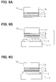
- FIGS. 8A and 8B are schematic cross sectional views explaining a method for manufacturing a semiconductor device according to a modification of the first embodiment
- FIGS. 9A to 9C are schematic cross sectional views explaining a method for manufacturing a semiconductor device according to a modification of the second embodiment.
- FIG. 10 is a graph showing a contact resistance between a P conductive type silicon substrate and an Al film or a Ti film, according to the modifications of the first and the second embodiments.
- FIGS. 1A and 1B A semiconductor device 100 according to a first embodiment of the present invention is shown in FIGS. 1A and 1B .
- FIG. 1A shows the device 100 before heat treatment, i.e., before soldering
- FIG. 1B shows the device 100 after heat treatment, i.e., after soldering.
- the device 100 includes a semiconductor substrate 1 and a base member 2 .
- the substrate 1 has an electric part such as a power transistor formed on a foreside of the substrate 1 .
- the backside of the substrate 1 which is opposite to the semiconductor part, is bonded on the base member 2 with a tin-based solder layer S.
- the base member 2 is, for example, a heat sink, a lead frame or a circuit board.
- the device 100 is manufactured as follows.
- the electric part is formed on the foreside of the substrate 1 .
- the first metal layer M and the second metal layer N are formed on the backside of the substrate 1 in this order.
- a semiconductor chip 10 is formed.
- the chip 10 is mounted on the base member 2 through the solder layer S, which is sandwiched between the base member 2 and the second metal layer N of the chip 10 .
- a stacked structure composing the chip 10 and the base member 2 is prepared.
- the stacked structure is heated so that the second metal layer is diffused into the solder layer S.
- the first metal layer M and the solder layer S are directly reacted so that an alloy layer T 1 is formed between the first metal layer M and the solder layer S.
- the alloy layer T 1 is made of alloy of the first metal layer M and the solder layer S. Specifically, the alloy layer T 1 is made of the first metal in the first metal layer M and tin in the solder layer S. After soldering, the device 100 is composed of the substrate 1 , the first metal layer M, the alloy layer T 1 , the solder layer S and the base member 2 . Here, the alloy layer T 1 works as a bonding layer between the chip 10 and the base member 2 .
- the first metal layer M is directly formed on the substrate 1 , another metal layer or an insulation layer can be formed between the substrate 1 and the first metal layer M.
- the backside of the substrate 1 is bonded to the base member 2 by using the minimum number of the metal layers and the tin-based solder layer S. Therefore, a manufacturing process of the device 100 is simple, and a manufacturing cost of the device 100 is low.
- the first metal in the first metal layer M is, for example, titanium (i.e., Ti), aluminum (i.e., Al), iron (i.e., Fe), molybdenum (i.e., Mo), chromium (i.e., Cr), vanadium (i.e., V) or iron-nickel-chromium alloy (i.e., Fe—Ni—Cr alloy).
- the first metal has excellent bonding property and excellent ohmic contact with a silicon substrate. Further, the first metal forms alloy with tin in the solder layer S. It is preferred that the first metal is made of Ti. Ti is a conventional material as a metallization material of silicon in the semiconductor substrate.
- Ti has excellent bonding property and excellent ohmic contact with the silicon substrate.
- a passive film such as an oxide film is easily formed on a Ti film.
- the second metal layer N is formed on the first metal layer M so that the second metal layer N works as a sacrifice layer for soldering.
- the alloy layer T 1 is formed between the first metal layer M and the solder layer S.
- the alloy layer T 1 has sufficiently strong bonding property.
- the thickness of the alloy layer T 1 is preferably equal to or thicker than 3 nm. More preferably, the thickness of the alloy layer T 1 is equal to or thicker than 10 nm.
- the average thickness of the alloy layer T 1 is equal to or larger than 10 nm, and the minimum thickness of the alloy layer T 1 at the interface between the first metal layer M and the solder layer S is equal to or larger than 3 nm, sufficiently strong bonding property is obtained. Further, when the thickness of the alloy layer T 1 is larger than 10 nm, almost the same bonding property as the case where the average thickness is equal to 10 nm is obtained.
- the second metal layer N is a thin film layer for protecting a surface of the first metal layer M from forming the passive film on the surface of the first metal layer M.
- the second metal layer N can be diffused into the solder layer S by the heat treatment of soldering so that the second metal layer N is disappeared after soldering.
- the thickness of the second metal layer N can be easily controlled.
- the soldering condition of the device 100 is easily controlled.
- the manufacturing cost of the device 100 becomes comparatively low.
- the thickness of the second metal layer N is preferably in a range between 50 nm and 750 nm, as described below.
- the second metal layer N may not sufficiently protect the first metal layer M from oxidizing the surface of the first metal layer M, i.e., from forming the passive film on the surface of the first metal layer M. Therefore, in this case, the solder-wettability of the solder layer S becomes smaller during the heat treatment, so that the bonding strength between the substrate 1 and the base member 2 becomes low.
- the thickness of the second metal layer N is larger than 50 nm, the bonding strength between the substrate 1 and the base member 2 becomes strong and constant.
- the second metal layer N is larger than 750 nm, the second metal layer N remains after soldering. Therefore, excess second metal layer may increase the manufacturing cost of the device 100 .
- first and the second metal layers M, N are formed serially in a vacuum chamber by using a physical vapor deposition (i.e., PVD) method such as a vacuum evaporation method and a sputtering method. Further, it is preferred that the degree of vacuum before deposition is equal to or smaller than 5 ⁇ 10 ⁇ 4 Pa. This is because the surface of the first metal layer M is prevented from oxidizing.
- PVD physical vapor deposition
- the second metal in the second metal layer N can be made of any metal. It is preferred that the second metal is nickel (i.e., Ni), copper (i.e., Cu), silver (i.e., Ag), gold (i.e., Au), platinum (i.e., Pt), silver-platinum (i.e., Ag—Pt) alloy, silver-palladium (i.e., Ag—Pd) alloy or palladium (i.e., Pd). More preferably, the second metal is nickel or gold. These second metals can form alloy with the first metal in the first metal layer M or tin in the solder layer S.
- the second metal layer N can be composed of a multi-layered film, which is made of the above metals.
- the second metal can be diffused into the solder layer S in the heat treatment process, i.e., in the soldering process. Further, the second metal can be involved into the alloy layer T 1 so that the alloy layer becomes the second alloy layer T 2 , as shown in FIGS. 6A and 6B .
- the tin-based solder layer S can be made of Pb-free solder, which does not include lead (i.e., Pb).
- Pb lead
- the device 100 can be manufactured with harmless and safety, so that environmental protection is obtained. It is preferred that the mass content of tin in the solder layer S is equal to or larger than 95 wt. %.
- the solder layer S is made of tin (i.e., Sn), tin-copper (i.e., Sn—Cu) alloy, tin-silver-copper (i.e., Sn—Ag—Cu) alloy, tin-copper-nickel (i.e., Sn—Cu—Ni) alloy, tin-antimony (i.e., Sn—Sb) alloy, tin-indium (i.e., Sn—In) alloy, or tin-zinc (i.e., Sn—Zn) alloy. More preferably, the solder layer S is made of pure Sn, Sn-(0.7 wt.
- the solder layer S can include additives such as phosphorous (i.e., P) and germanium (i.e., Ge).
- the device 100 is manufactured, for example, as follows.
- a Ti film having the thickness of 250 nm is formed on the backside of the substrate 1 so that the first metal layer M is formed on the substrate 1 .
- the second metal layer N composed of a Ni film having the thickness in a range between 50 nm and 1000 nm and an Au film having the thickness of 50 nm is formed on the first metal layer M.
- the second metal layer N is made of a multi-layered film.
- the solder layer S made of (99.24 wt. % Sn)-(0.7 wt. % Cu)-(0.06 wt. % Ni) alloy is formed on the base member 2 .
- the base member 2 is made of metal.
- the semiconductor chip 10 including the substrate 1 with the first and the second metal layers M, N is mounted on the base member 2 through the solder layer S. Then, the chip 10 with the base member 2 is mounted in a hydrogen reduction atmospheric furnace. In the furnace, the chip 10 with the base member 2 is heated up to 270° C., which is higher than the solidus temperature of the solder layer S. Here, the solidus temperature is about 220° C. Thus, the chip 10 with the base member 2 is heated up to the peak temperature of 270° C. during 20 seconds so that the solder layer S is reflowed. In this heat treatment process, i.e., in this soldering process, the chip 10 is soldered on the base member 2 .
- the cross section of the device 100 after soldering is studied.
- the thickness of the Ni film is equal to or smaller than 750 nm
- the second metal layer N composed of the Ni film and the Au film is diffused into the solder layer S so that the first alloy layer T 1 composed of Ti and Sn is formed.
- the thickness of the Ni film is larger than 750 nm
- the Ni film in the second metal layer N remains. This unreacted Ni film does not contribute to the bonding between the chip 10 and the base member 2 . Accordingly, to reduce the manufacturing cost of the device 100 , it is preferred that the thickness of the Ni film is equal to or smaller than 750 nm.
- FIG. 2 shows defective percentage of the device 100 having different thickness of the Ni film.
- the defect of the device 100 is caused by defective solder wetting.
- FIG. 3 shows tensile strength of the device 100 having different thickness of the Ni film. Here, ten samples of the device 100 in each thickness of the Ni film are studied.
- the bonding strength between the substrate 1 and the base member 2 is weak. This is because the thickness of the Ni film is thin so that the second metal layer N cannot protect the first metal layer M from oxidizing. In this case, the surface of the Ti film of the first metal layer M is oxidized. Accordingly, it is required for the Ni film to becomes thicker than 50 nm to prevent the Ti film from oxidizing. When the thickness of the Ni film is larger than 50 nm, the sufficiently strong bonding strength is obtained.
- FIG. 4 shows tensile strength of the device 100 having different thickness of the Au film.
- the second metal layer N of the device 100 is composed of only an Au film. Therefore, the Ni film is not formed in the second metal layer N.
- ten samples of the device 100 in each thickness of the Au film are studied. When the thickness of the Au film is 50 nm, the defective solder wetting is occurred. However, when the thickness of the Au film is larger than 50 nm, the sufficiently strong bonding strength is obtained.
- FIG. 5 shows a result of elemental analysis of the cross section of a bonding layer in the device 100 .
- the device 100 has the first metal layer M made of molybdenum (i.e., Mo) and the second metal layer N made of Ni.
- the elemental analysis is performed in a thickness direction.
- FIG. 5 shows a depth profile of the elemental analysis.
- Ni in the second metal layer N is diffused into the solder layer S so that the first alloy layer Ti composed of Mo—Sn alloy is formed.
- FIGS. 6A to 6C A semiconductor device 101 according to a second embodiment of the present invention is shown in FIGS. 6A to 6C .
- FIG. 6A shows the chip 10 before the first heat treatment
- FIG. 6B shows the chip 10 after the first heat treatment and the base member 2 before soldering
- FIG. 6C shows the device 101 after the second heat treatment, i.e., after the soldering.
- the device 101 is manufactured as follows. Firstly, the first metal layer M and the second metal layer N are formed on the backside of the substrate 1 in this order so that the semiconductor chip 10 is prepared. The chip 10 is firstly heated so that an intermediate alloy layer O is formed. The intermediate alloy layer O is composed of the first metal and the second metal alloy. The intermediate alloy layer O is disposed between the first and the second metal layers M, N. After this first heat treatment, the chip 10 is mounted on the base member 2 through the solder layer S. Then, the chip 10 with the base member 2 is heated secondary so that the chip 10 is soldered on the base member 2 .
- the second metal layer N is diffused into the solder layer S, and further, the intermediate alloy layer O is reacted to the solder layer S so that the second alloy layer T 2 is formed.
- the second alloy layer T 2 is composed of the first metal in the first metal layer M, the second metal in the second metal layer N and Sn in the solder layer S.
- the device 101 includes the base member 2 , the solder layer S, the second alloy layer T 2 , the first metal layer M and the substrate 1 .
- the second alloy layer T 2 works as a bonding layer between the chip 10 and the base member 2 .
- the backside of the substrate 1 is bonded to the base member 2 by using the minimum number of the metal layers and the tin-based solder layer S. Therefore, a manufacturing process of the device 101 is simple, and a manufacturing cost of the device 101 is low.
- the second metal in the second metal layer N is Ni, Cu, Ag, Au, Pt, Ag—Pt alloy, Ag—Pd alloy or Pd. More preferably, the second metal is Ni or Au.
- the second metal can form alloy with Ti in a case where the first metal layer is made of Ti.
- the device 101 is manufactured, for example, as follows.
- the first metal layer M made of a Ti film having the thickness of 250 nm is formed on the backside of the substrate 1 .
- the second metal layer N composed of a Ni film having the thickness in a range between 50 nm and 600 nm and an Au film having the thickness of 50 nm is formed on the first metal layer M.
- the second metal layer N is made of a multi-layered film.
- the chip 10 is prepared, and then, the chip is heated at 380° C. during three minutes. Then, the cross section of the chip 10 is studied. As a result, the intermediate alloy layer O having the thickness of 20 nm is formed between the first metal layer M and the second metal layer N.
- the solder layer S made of (99.24 wt. % Sn)-(0.7 wt. % Cu)-(0.06 wt. % Ni) alloy is formed on the base member 2 made of metal.
- the chip 10 is mounted on the base member 2 through the solder layer S.
- the chip 10 with the base member 2 is mounted in a hydrogen reduction atmospheric furnace. In the furnace, the chip 10 with the base member 2 is heated up to 270° C., which is higher than the solidus temperature of the solder layer S.
- the solidus temperature is about 220° C.
- the chip 10 with the base member 2 is heated up to the peak temperature of 270° C. during 20 seconds so that the solder layer S is reflowed.
- the chip 10 is soldered on the base member 2 .
- the second alloy layer T 2 is formed.
- the second alloy layer T 2 is made of Ti—Sn—Ni alloy.
- FIG. 7A shows time change of thickness of the Ti film of the first metal layer M in a case where the device 100 shown in FIG. 1B includes the first alloy layer T 1 composed of the Ti—Sn alloy.
- FIG. 7B shows time change of thickness of the Ti film of the first metal layer M in a case where the device 101 shown in FIG. 6C includes the second alloy layer T 2 composed of the Ti—Sn—Ni alloy.
- the devices 100 , 101 are performed under 150° C. endurance test during 0 hour, 1000 hours or 2000 hours.
- 0 hour means that the devices 100 , 101 are not performed under the endurance test.
- FIG. 1B shows time change of thickness of the Ti film of the first metal layer M in a case where the device 100 shown in FIG. 1B includes the first alloy layer T 1 composed of the Ti—Sn alloy.
- FIG. 7B shows time change of thickness of the Ti film of the first metal layer M in a case where the device 101 shown in FIG. 6C includes the second alloy layer T 2 composed of the Ti—Sn—N
- a line VIIA represents the device 100 with the Ni film having the initial thickness of 600 nm before soldering
- a line VIIB represents the device 100 with the Ni film having the initial thickness of 200 nm before soldering
- a line VIIC represents the device 100 with the Ni film having the initial thickness of 50 nm before soldering
- a line VIID represents the device 101 with the Ni film having the initial thickness of 600 nm before soldering
- a line VIIE represents the device 101 with the Ni film having the initial thickness of 200 nm before soldering
- a line VIIF represents the device 101 with the Ni film having the initial thickness of 50 nm before soldering.
- the time change of the thickness of the Ti film is comparatively small, compared with the device 100 having the first alloy layer T 1 . Therefore, in the device 101 , Ti in the first metal layer M and Sn in the solder layer S are slowly reacted during a high temperature endurance test, compared with the device 100 .
- the substrate 1 can be made of any semiconductor material.
- the third metal layer L is formed between the first metal layer M and the substrate 1 p , as shown in FIGS. 8A to 9C .
- the third metal layer L is made of aluminum based material.
- the third metal layer L is made of pure aluminum (i.e., Al), aluminum-silicon (i.e., Al—Si) alloy, or aluminum-silicon-copper (i.e., Al—Si—Cu) alloy.
- FIG. 10 shows a contact resistance between a P conductive type silicon substrate 1 p and an Al layer or a Ti layer.
- the contact resistance between the P conductive type silicon substrate 1 p and the Al layer is much lower than that between the P conductive type silicon substrate and the Ti layer.
- the contact resistance of the Al layer is three orders of magnitude less than that of the Ti layer. Accordingly, the devices 100 , 101 having the third metal layer L have excellent conductivity between the P conductive type semiconductor substrate 1 p and the base member 2 .
- the chip 10 is bonded to the base member 2 by a solder reflow method in the hydrogen reduction atmospheric furnace
- the chip 10 can be bonded to the base member 2 by using other soldering method such as a solder die bonding method with a wire solder and an air or an inert gas atmospheric reflow method with a solder paste.
Landscapes
- Engineering & Computer Science (AREA)
- Computer Hardware Design (AREA)
- Microelectronics & Electronic Packaging (AREA)
- Power Engineering (AREA)
- Chemical & Material Sciences (AREA)
- Materials Engineering (AREA)
- Physics & Mathematics (AREA)
- Condensed Matter Physics & Semiconductors (AREA)
- General Physics & Mathematics (AREA)
- Die Bonding (AREA)
Abstract
Description
Claims (16)
Priority Applications (1)
| Application Number | Priority Date | Filing Date | Title |
|---|---|---|---|
| US11/707,961 US7579212B2 (en) | 2004-09-08 | 2007-02-20 | Semiconductor device having tin-based solder layer and method for manufacturing the same |
Applications Claiming Priority (6)
| Application Number | Priority Date | Filing Date | Title |
|---|---|---|---|
| JP2004261425 | 2004-09-08 | ||
| JP2004-261425 | 2004-09-08 | ||
| JP2004-368114 | 2004-12-20 | ||
| JP2004368114A JP4882229B2 (en) | 2004-09-08 | 2004-12-20 | Semiconductor device and manufacturing method thereof |
| US11/220,979 US7361996B2 (en) | 2004-09-08 | 2005-09-08 | Semiconductor device having tin-based solder layer and method for manufacturing the same |
| US11/707,961 US7579212B2 (en) | 2004-09-08 | 2007-02-20 | Semiconductor device having tin-based solder layer and method for manufacturing the same |
Related Parent Applications (1)
| Application Number | Title | Priority Date | Filing Date |
|---|---|---|---|
| US11/220,979 Division US7361996B2 (en) | 2004-09-08 | 2005-09-08 | Semiconductor device having tin-based solder layer and method for manufacturing the same |
Publications (2)
| Publication Number | Publication Date |
|---|---|
| US20070176293A1 US20070176293A1 (en) | 2007-08-02 |
| US7579212B2 true US7579212B2 (en) | 2009-08-25 |
Family
ID=35852775
Family Applications (2)
| Application Number | Title | Priority Date | Filing Date |
|---|---|---|---|
| US11/220,979 Active 2025-11-19 US7361996B2 (en) | 2004-09-08 | 2005-09-08 | Semiconductor device having tin-based solder layer and method for manufacturing the same |
| US11/707,961 Active 2026-05-07 US7579212B2 (en) | 2004-09-08 | 2007-02-20 | Semiconductor device having tin-based solder layer and method for manufacturing the same |
Family Applications Before (1)
| Application Number | Title | Priority Date | Filing Date |
|---|---|---|---|
| US11/220,979 Active 2025-11-19 US7361996B2 (en) | 2004-09-08 | 2005-09-08 | Semiconductor device having tin-based solder layer and method for manufacturing the same |
Country Status (3)
| Country | Link |
|---|---|
| US (2) | US7361996B2 (en) |
| JP (1) | JP4882229B2 (en) |
| DE (1) | DE102005042780B4 (en) |
Families Citing this family (26)
| Publication number | Priority date | Publication date | Assignee | Title |
|---|---|---|---|---|
| JP2007110016A (en) * | 2005-10-17 | 2007-04-26 | Denso Corp | Semiconductor device and method of manufacturing same |
| US20070117475A1 (en) * | 2005-11-23 | 2007-05-24 | Regents Of The University Of California | Prevention of Sn whisker growth for high reliability electronic devices |
| JP4221012B2 (en) * | 2006-06-12 | 2009-02-12 | トヨタ自動車株式会社 | Semiconductor device and manufacturing method thereof |
| WO2008060447A2 (en) * | 2006-11-09 | 2008-05-22 | Quantum Leap Packaging, Inc. | Microcircuit package having ductile layer |
| US8314500B2 (en) * | 2006-12-28 | 2012-11-20 | Ultratech, Inc. | Interconnections for flip-chip using lead-free solders and having improved reaction barrier layers |
| US9214442B2 (en) * | 2007-03-19 | 2015-12-15 | Infineon Technologies Ag | Power semiconductor module, method for producing a power semiconductor module, and semiconductor chip |
| KR100893567B1 (en) * | 2007-08-14 | 2009-04-17 | 앰코 테크놀로지 코리아 주식회사 | Semiconductor package and method for manufacturing the same |
| JP5331322B2 (en) * | 2007-09-20 | 2013-10-30 | 株式会社日立製作所 | Semiconductor device |
| JP2009010421A (en) * | 2008-10-01 | 2009-01-15 | Toyota Motor Corp | Method for mounting semiconductor device on circuit board |
| JPWO2010109572A1 (en) | 2009-03-23 | 2012-09-20 | トヨタ自動車株式会社 | Semiconductor device |
| JP5465942B2 (en) * | 2009-07-16 | 2014-04-09 | ルネサスエレクトロニクス株式会社 | Semiconductor device and manufacturing method thereof |
| US8803452B2 (en) * | 2010-10-08 | 2014-08-12 | Soraa, Inc. | High intensity light source |
| JP5772050B2 (en) * | 2011-02-22 | 2015-09-02 | 富士通株式会社 | Semiconductor device, manufacturing method thereof, and power supply device |
| TW201250849A (en) * | 2011-06-14 | 2012-12-16 | 3S Silicon Tech Inc | Low-temperature chip bonding method for light-condensing type solar chip, power transistor and field effect transistor |
| JP5976379B2 (en) * | 2012-04-26 | 2016-08-23 | 株式会社東芝 | Electronic device and manufacturing method thereof |
| US20130308274A1 (en) * | 2012-05-21 | 2013-11-21 | Triquint Semiconductor, Inc. | Thermal spreader having graduated thermal expansion parameters |
| JP6046010B2 (en) * | 2013-09-09 | 2016-12-14 | 株式会社東芝 | Semiconductor device and manufacturing method thereof |
| JP6424610B2 (en) | 2014-04-23 | 2018-11-21 | ソニー株式会社 | Semiconductor device and manufacturing method |
| JP6356478B2 (en) * | 2014-05-09 | 2018-07-11 | 新日本無線株式会社 | Manufacturing method of semiconductor device |
| JP6639188B2 (en) | 2015-10-21 | 2020-02-05 | ソニーセミコンダクタソリューションズ株式会社 | Semiconductor device and manufacturing method |
| GB2557439B (en) * | 2016-10-24 | 2021-06-30 | Jaguar Land Rover Ltd | Apparatus and method relating to electrochemical migration |
| JP6643749B2 (en) * | 2017-10-31 | 2020-02-12 | 千住金属工業株式会社 | Solder joint and method of forming solder joint |
| JP2019102772A (en) * | 2017-12-08 | 2019-06-24 | トヨタ自動車株式会社 | Semiconductor device manufacturing method |
| WO2019116910A1 (en) | 2017-12-13 | 2019-06-20 | 三菱電機株式会社 | Semiconductor device and method for producing semiconductor device |
| JP2022188702A (en) * | 2021-06-09 | 2022-12-21 | 日立Astemo株式会社 | Semiconductor device and method of manufacturing semiconductor device |
| US20230232561A1 (en) * | 2021-12-21 | 2023-07-20 | ColdQuanta, Inc. | Method and system for providing multiple seals for a compact vacuum cell |
Citations (19)
| Publication number | Priority date | Publication date | Assignee | Title |
|---|---|---|---|---|
| US3741880A (en) | 1969-10-25 | 1973-06-26 | Nippon Electric Co | Method of forming electrical connections in a semiconductor integrated circuit |
| JPS52147064A (en) | 1976-06-01 | 1977-12-07 | Mitsubishi Electric Corp | Semiconductor device |
| JPS58182840A (en) | 1982-04-21 | 1983-10-25 | Matsushita Electronics Corp | Semiconductor device |
| JPS62163335A (en) | 1986-01-14 | 1987-07-20 | Toshiba Corp | Semiconductor device |
| US4954870A (en) * | 1984-12-28 | 1990-09-04 | Kabushiki Kaisha Toshiba | Semiconductor device |
| JPH05160533A (en) | 1991-12-06 | 1993-06-25 | Hitachi Ltd | Circuit board and electronic apparatus using the same |
| JPH06244226A (en) | 1993-02-19 | 1994-09-02 | Hitachi Ltd | Semiconductor device and manufacture thereof |
| US5731635A (en) | 1995-07-27 | 1998-03-24 | U.S. Philips Corporation | Semiconductor device having a carrier and a multilayer metallization |
| JP2000100846A (en) | 1998-09-17 | 2000-04-07 | Fujitsu Ltd | Bump and its manufacture |
| JP2001077049A (en) | 1999-09-06 | 2001-03-23 | Toshiba Corp | Semiconductor element, semiconductor device, and manufacture of semiconductor device |
| US20010019882A1 (en) * | 1997-12-16 | 2001-09-06 | Tongbi Jiang | Method of making electrical interconnection for attachment to a substrate |
| US20020093096A1 (en) | 2001-01-15 | 2002-07-18 | Nec Corporation | Semiconductor device, manufacturing method and apparatus for the same |
| US6515372B1 (en) | 1999-02-26 | 2003-02-04 | Hitachi, Ltd. | Wiring board and its production method, semiconductor device and its production method, and electronic apparatus |
| JP2003152007A (en) | 2001-11-12 | 2003-05-23 | Hitachi Ltd | Bump forming method and mounting structure of semiconductor device |
| JP2003347487A (en) | 2002-05-29 | 2003-12-05 | Nec Kansai Ltd | Semiconductor device |
| US6805974B2 (en) * | 2002-02-15 | 2004-10-19 | International Business Machines Corporation | Lead-free tin-silver-copper alloy solder composition |
| US20040211665A1 (en) * | 2001-07-25 | 2004-10-28 | Yoon Ki Hwan | Barrier formation using novel sputter-deposition method |
| US20040232429A1 (en) | 1997-05-08 | 2004-11-25 | Showa Denko K.K. | Electrode for light-emitting semiconductor devices and method of producing the electrode |
| JP2005037239A (en) | 2003-07-14 | 2005-02-10 | Denso Corp | Mounting structure of sensor device |
Family Cites Families (8)
| Publication number | Priority date | Publication date | Assignee | Title |
|---|---|---|---|---|
| JPS61156825A (en) * | 1984-12-28 | 1986-07-16 | Toshiba Corp | Semiconductor device |
| JPS61156823A (en) * | 1984-12-28 | 1986-07-16 | Toshiba Corp | Semiconductor device |
| JPH04352432A (en) * | 1991-05-30 | 1992-12-07 | Toshiba Corp | Semiconductor device and manufacture thereof |
| DE9212486U1 (en) * | 1992-09-16 | 1993-03-04 | Siemens AG, 8000 München | Semiconductor body with soldered carrier plate |
| DE19603654C1 (en) * | 1996-02-01 | 1997-07-03 | Siemens Ag | Method for soldering a semiconductor body to a carrier plate and semiconductor body for carrying out the method |
| DE19606101A1 (en) * | 1996-02-19 | 1997-08-21 | Siemens Ag | Semiconductor body with solder material layer |
| JP2000353709A (en) * | 1999-06-14 | 2000-12-19 | Hitachi Ltd | Semiconductor device and electronic component using the same |
| JP2005026612A (en) * | 2003-07-02 | 2005-01-27 | Denso Corp | Semiconductor device |
-
2004
- 2004-12-20 JP JP2004368114A patent/JP4882229B2/en not_active Expired - Fee Related
-
2005
- 2005-09-08 DE DE102005042780.4A patent/DE102005042780B4/en not_active Expired - Fee Related
- 2005-09-08 US US11/220,979 patent/US7361996B2/en active Active
-
2007
- 2007-02-20 US US11/707,961 patent/US7579212B2/en active Active
Patent Citations (19)
| Publication number | Priority date | Publication date | Assignee | Title |
|---|---|---|---|---|
| US3741880A (en) | 1969-10-25 | 1973-06-26 | Nippon Electric Co | Method of forming electrical connections in a semiconductor integrated circuit |
| JPS52147064A (en) | 1976-06-01 | 1977-12-07 | Mitsubishi Electric Corp | Semiconductor device |
| JPS58182840A (en) | 1982-04-21 | 1983-10-25 | Matsushita Electronics Corp | Semiconductor device |
| US4954870A (en) * | 1984-12-28 | 1990-09-04 | Kabushiki Kaisha Toshiba | Semiconductor device |
| JPS62163335A (en) | 1986-01-14 | 1987-07-20 | Toshiba Corp | Semiconductor device |
| JPH05160533A (en) | 1991-12-06 | 1993-06-25 | Hitachi Ltd | Circuit board and electronic apparatus using the same |
| JPH06244226A (en) | 1993-02-19 | 1994-09-02 | Hitachi Ltd | Semiconductor device and manufacture thereof |
| US5731635A (en) | 1995-07-27 | 1998-03-24 | U.S. Philips Corporation | Semiconductor device having a carrier and a multilayer metallization |
| US20040232429A1 (en) | 1997-05-08 | 2004-11-25 | Showa Denko K.K. | Electrode for light-emitting semiconductor devices and method of producing the electrode |
| US20010019882A1 (en) * | 1997-12-16 | 2001-09-06 | Tongbi Jiang | Method of making electrical interconnection for attachment to a substrate |
| JP2000100846A (en) | 1998-09-17 | 2000-04-07 | Fujitsu Ltd | Bump and its manufacture |
| US6515372B1 (en) | 1999-02-26 | 2003-02-04 | Hitachi, Ltd. | Wiring board and its production method, semiconductor device and its production method, and electronic apparatus |
| JP2001077049A (en) | 1999-09-06 | 2001-03-23 | Toshiba Corp | Semiconductor element, semiconductor device, and manufacture of semiconductor device |
| US20020093096A1 (en) | 2001-01-15 | 2002-07-18 | Nec Corporation | Semiconductor device, manufacturing method and apparatus for the same |
| US20040211665A1 (en) * | 2001-07-25 | 2004-10-28 | Yoon Ki Hwan | Barrier formation using novel sputter-deposition method |
| JP2003152007A (en) | 2001-11-12 | 2003-05-23 | Hitachi Ltd | Bump forming method and mounting structure of semiconductor device |
| US6805974B2 (en) * | 2002-02-15 | 2004-10-19 | International Business Machines Corporation | Lead-free tin-silver-copper alloy solder composition |
| JP2003347487A (en) | 2002-05-29 | 2003-12-05 | Nec Kansai Ltd | Semiconductor device |
| JP2005037239A (en) | 2003-07-14 | 2005-02-10 | Denso Corp | Mounting structure of sensor device |
Non-Patent Citations (6)
| Title |
|---|
| Chinese Office Action issued from the Chinese Patent Office dated Jul. 6, 2007 in the corresponding Chinese application No. 200510099909.8 (and English translation). |
| Materials Database Station and National Institute for Materials Science, "Soldering Technique for Electronic Material," Fig. 3.3, (Sep. 5, 1983), pp. 41-43, 318 (and Partial English Translation of text from Figure 3.3). |
| Materials Database Station and National Institute for Materials Science, "Technique for Soldering Process," Table 5.2, Note (b), (Feb. 28, 1981), pp. 130-133 (and Partial English Translation of Note(b) of Table 5.2). |
| Ng, Kwok K., Complete Guide to Semiconductor Devices, Second Edition, John Wiley and Sons, Inc., 2005, Appendix B2 p. 600. |
| Office Action from U.S. Patent Office issued on Mar. 13, 2007 for the corresponding U.S. Appl. No. 11/220,979. |
| United States Office Action from the USPTO dated Aug. 6, 2007 in the parent U.S. Appl. No. 11/220,979. |
Also Published As
| Publication number | Publication date |
|---|---|
| DE102005042780A1 (en) | 2006-03-09 |
| JP4882229B2 (en) | 2012-02-22 |
| US20060049521A1 (en) | 2006-03-09 |
| JP2006108604A (en) | 2006-04-20 |
| US7361996B2 (en) | 2008-04-22 |
| US20070176293A1 (en) | 2007-08-02 |
| DE102005042780B4 (en) | 2017-02-02 |
Similar Documents
| Publication | Publication Date | Title |
|---|---|---|
| US7579212B2 (en) | Semiconductor device having tin-based solder layer and method for manufacturing the same | |
| CN100452372C (en) | Semiconductor device having tin-based solder layer and method for manufacturing the same | |
| US20210167034A1 (en) | Chip arrangements | |
| US5367195A (en) | Structure and method for a superbarrier to prevent diffusion between a noble and a non-noble metal | |
| EP0097833B1 (en) | Substrate for integrated circuit packages | |
| US9943930B2 (en) | Composition of a solder, and method of manufacturing a solder connection | |
| US20080136019A1 (en) | Solder Bump/Under Bump Metallurgy Structure for High Temperature Applications | |
| CN103123916B (en) | Semiconductor device, electronic device and method, semi-conductor device manufacturing method | |
| WO2006098454A1 (en) | Submount and method for manufacturing same | |
| JP2006520103A (en) | Flip chip coated metal stud bumps made of coated wire | |
| CN109755208B (en) | Bonding material, semiconductor device and manufacturing method thereof | |
| JP3372548B2 (en) | Surface treatment structure for solder joining and fluxless soldering method using the same | |
| US20060210790A1 (en) | Thermoelectric module and solder therefor | |
| JP2008543035A (en) | UBM pad, solder contact and solder joining method | |
| CN107431000A (en) | There are the metal bond pads of cobalt interconnection layer and solder thereon | |
| WO2010047010A1 (en) | Semiconductor device and method for manufacturing the same | |
| JP2006278463A (en) | Sub-mount | |
| US8071472B2 (en) | Semiconductor device with solder balls having high reliability | |
| JP2005032834A (en) | Joining method of semiconductor chip and substrate | |
| US20230126663A1 (en) | Layer structure and chip package that includes the layer structure | |
| JP2701419B2 (en) | Gold alloy fine wire for semiconductor element and bonding method thereof | |
| JP2004106027A (en) | Brazing filler metal, semi-conductor device assembling method and semi-conductor device using the same | |
| US7644855B2 (en) | Brazing filler metal, assembly method for semiconductor device using same, and semiconductor device | |
| JP2007110016A (en) | Semiconductor device and method of manufacturing same |
Legal Events
| Date | Code | Title | Description |
|---|---|---|---|
| STCF | Information on status: patent grant |
Free format text: PATENTED CASE |
|
| FEPP | Fee payment procedure |
Free format text: PAYOR NUMBER ASSIGNED (ORIGINAL EVENT CODE: ASPN); ENTITY STATUS OF PATENT OWNER: LARGE ENTITY |
|
| FEPP | Fee payment procedure |
Free format text: PAYOR NUMBER ASSIGNED (ORIGINAL EVENT CODE: ASPN); ENTITY STATUS OF PATENT OWNER: LARGE ENTITY Free format text: PAYER NUMBER DE-ASSIGNED (ORIGINAL EVENT CODE: RMPN); ENTITY STATUS OF PATENT OWNER: LARGE ENTITY |
|
| FPAY | Fee payment |
Year of fee payment: 4 |
|
| FPAY | Fee payment |
Year of fee payment: 8 |
|
| MAFP | Maintenance fee payment |
Free format text: PAYMENT OF MAINTENANCE FEE, 12TH YEAR, LARGE ENTITY (ORIGINAL EVENT CODE: M1553); ENTITY STATUS OF PATENT OWNER: LARGE ENTITY Year of fee payment: 12 |