US7420869B2 - Memory device, use thereof and method for synchronizing a data word - Google Patents
Memory device, use thereof and method for synchronizing a data word Download PDFInfo
- Publication number
- US7420869B2 US7420869B2 US11/412,755 US41275506A US7420869B2 US 7420869 B2 US7420869 B2 US 7420869B2 US 41275506 A US41275506 A US 41275506A US 7420869 B2 US7420869 B2 US 7420869B2
- Authority
- US
- United States
- Prior art keywords
- input
- clock
- data
- signal
- output
- Prior art date
- Legal status (The legal status is an assumption and is not a legal conclusion. Google has not performed a legal analysis and makes no representation as to the accuracy of the status listed.)
- Expired - Fee Related, expires
Links
- 238000000034 method Methods 0.000 title description 8
- 230000004913 activation Effects 0.000 claims description 10
- 230000001360 synchronised effect Effects 0.000 abstract description 20
- 238000012546 transfer Methods 0.000 abstract description 7
- 230000006870 function Effects 0.000 description 9
- 238000010586 diagram Methods 0.000 description 6
- 230000000630 rising effect Effects 0.000 description 6
- 238000012360 testing method Methods 0.000 description 3
- 230000008901 benefit Effects 0.000 description 2
- 230000005540 biological transmission Effects 0.000 description 2
- 230000008859 change Effects 0.000 description 2
- 230000000694 effects Effects 0.000 description 2
- 230000009471 action Effects 0.000 description 1
- 230000004075 alteration Effects 0.000 description 1
- 230000000712 assembly Effects 0.000 description 1
- 238000000429 assembly Methods 0.000 description 1
- 238000006243 chemical reaction Methods 0.000 description 1
- 238000004891 communication Methods 0.000 description 1
- 230000008878 coupling Effects 0.000 description 1
- 238000010168 coupling process Methods 0.000 description 1
- 238000005859 coupling reaction Methods 0.000 description 1
- 230000001419 dependent effect Effects 0.000 description 1
- 238000013461 design Methods 0.000 description 1
- 238000011156 evaluation Methods 0.000 description 1
- 238000012986 modification Methods 0.000 description 1
- 230000004048 modification Effects 0.000 description 1
- 238000012545 processing Methods 0.000 description 1
- 230000004044 response Effects 0.000 description 1
- 230000008054 signal transmission Effects 0.000 description 1
- 238000011144 upstream manufacturing Methods 0.000 description 1
Images


Classifications
-
- G—PHYSICS
- G11—INFORMATION STORAGE
- G11C—STATIC STORES
- G11C5/00—Details of stores covered by group G11C11/00
- G11C5/06—Arrangements for interconnecting storage elements electrically, e.g. by wiring
- G11C5/066—Means for reducing external access-lines for a semiconductor memory clip, e.g. by multiplexing at least address and data signals
-
- G—PHYSICS
- G11—INFORMATION STORAGE
- G11C—STATIC STORES
- G11C7/00—Arrangements for writing information into, or reading information out from, a digital store
- G11C7/10—Input/output [I/O] data interface arrangements, e.g. I/O data control circuits, I/O data buffers
- G11C7/1078—Data input circuits, e.g. write amplifiers, data input buffers, data input registers, data input level conversion circuits
- G11C7/1087—Data input latches
-
- G—PHYSICS
- G11—INFORMATION STORAGE
- G11C—STATIC STORES
- G11C7/00—Arrangements for writing information into, or reading information out from, a digital store
- G11C7/10—Input/output [I/O] data interface arrangements, e.g. I/O data control circuits, I/O data buffers
- G11C7/1078—Data input circuits, e.g. write amplifiers, data input buffers, data input registers, data input level conversion circuits
- G11C7/1093—Input synchronization
-
- H—ELECTRICITY
- H04—ELECTRIC COMMUNICATION TECHNIQUE
- H04L—TRANSMISSION OF DIGITAL INFORMATION, e.g. TELEGRAPHIC COMMUNICATION
- H04L7/00—Arrangements for synchronising receiver with transmitter
-
- H—ELECTRICITY
- H04—ELECTRIC COMMUNICATION TECHNIQUE
- H04L—TRANSMISSION OF DIGITAL INFORMATION, e.g. TELEGRAPHIC COMMUNICATION
- H04L7/00—Arrangements for synchronising receiver with transmitter
- H04L7/0008—Synchronisation information channels, e.g. clock distribution lines
Definitions
- the present invention relates to a memory device and to a method for synchronizing a data word.
- the invention also relates to a use of the memory device for synchronizing data on a three-wire bus.
- Modern integrated radio-frequency chips have a large number of settable parameters and functions. These include, inter alia, various test functions which check that the individual areas of the radio-frequency chip are operable. In addition, different operating parameters can be set in order to optimize the radio-frequency chip for a particular, partly selectable application.
- the various functions and settable parameters are no longer actuated via individual control lines, however, but rather the radio-frequency chip communicates with an appropriate control unit via a serial interface. This control unit is also called a host.
- a serial programming interface which has found to be particularly advantageous is one with three lines.
- This three-wire system is also called a three-wire bus.
- the bus comprises a clock line, a data line and an activation or Enable line. Communication between the control chip and the radio-frequency chip is controlled and driven by the control chip. Following activation of the programming interface by a signal on the Enable line, the control chip outputs a clock signal on the clock line. At the same time, a number of data bits are output on the data line, with preferably each clock edge of the clock signal on the clock line always appearing in the middle of a bit period of a data bit.
- the radio-frequency chip stores the number of data bits upon every clock edge on the clock line for as long as the signal is present on the Enable line.
- the signal on the Enable line contains two possible states which can be adopted, with a first state existing whenever the control chip is transmitting data to the radio-frequency chip via the serial programming interface.
- the number of data bits on the data line is dependent on various external parameters.
- the situation is that the data bits are combined to form a “message” or data word and are respectively stored in a register of a memory in the radio-frequency chip.
- a data word with a length of 24 bits has been found to be preferred.
- a number of the 24 bits are defined as an address at the end of the message, so that various registers of the memory can be addressed directly within the radio-frequency chip.
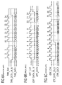
- FIG. 6A shows the clock signal TWB_CLK on the clock line, the signals TWB_DATA on the data line and also the signal TWB_DATA_EN_N on the Enable line of a three-wire bus. It can be seen that a rising clock edge in the clock signal TWB_CLK always appears in the middle of a data bit TWB_DATA.
- the signal TWB_DATA_EN_N on the Enable line is pulled to the logic low state “Low”, and hence it is indicated that data are present on the data line.
- the message length is independent provided that the entire message with its data bits is guaranteed to be able to be stored within a register in the radio-frequency chip.
- DiagRF digital RF standard
- the signals used for this are of similar structure to the signals in the illustration shown in FIG. 6A .
- the clock signal TWB_CLK which is used to write the data to the radio-frequency chip or to read them from it, is usually generated by an external clock generator.
- the clock signal TWB CLK therefore has an asynchronous profile relative to a system clock which is used and generated internally by the radio-frequency chip. It is therefore necessary to synchronize the data word which is to be transmitted, so that a possible loss of data is avoided. In this case, the synchronization needs to take place at least before the data are processed.
- the term synchronization is subsequently understood to mean the acceptance or output of data between two circuits which use different clock signals.
- the invention is directed to a memory device which allows provision to be made for data supplied to the memory device externally to be synchronized at a central point.
- the invention is also directed to a method which allows simple means to be used to synchronize data.
- the memory device comprises a register device having a data input and a clock input.
- the register device is configured to accept a parallel data word on its data input on the basis of a clock signal on the clock input.
- the data input of the register device has a multiplexer connected thereto which takes a signal on its control input as a basis for coupling one of its two data inputs to its data output.
- a buffer store is provided whose output is connected to the two data outputs.
- the buffer store is configured to accept a serial data word on a data input of the memory device on the basis of signals on a first clock input of the memory device and on a state input of the memory device.
- the accepted data word is output by the buffer store to one of the two data outputs as a parallel data word.
- the buffer store ensures that synchronization between an external first clock signal on the first clock input of the memory device and a further internal clock signal on a second clock input of the memory device is possible.
- a synchronization circuit is provided in one embodiment which has a control output connected to the control input of the multiplexer.
- the synchronization circuit has a clock signal input which is connected to the clock input of the register device.
- the synchronization circuit is configured to output a clock signal to the clock signal output, wherein the clock signal is produced from a time profile for a signal on the state input and from a signal on the second clock input.
- the register device accepts a parallel data word which is output by the buffer store on one of its two data outputs in sync with the second clock signal on the second clock input of the memory device.
- this involves the time profile of a signal on the state input and a clock edge of the signal on the state input being registered by the synchronization circuit. This very clock edge is synchronized to the signal on the second clock input in accordance with one embodiment of the invention.
- the synchronization circuit allows the data word to be transferred from the buffer store to the register device even in the absence of a signal on the second clock input, that is to say when there is no second clock signal.
- the synchronization circuit comprises a circuit having a control output whose output forms the clock signal output.
- a first input of the switch is connected to the state input and a second input of the switch is connected to a clock generator.
- the switch is configured to selectively couple one of its two inputs to its output on the basis of a synchronization signal.
- the synchronization signal advantageously indicates whether a second clock signal is being applied to the second clock input of the memory device. If so, the switch in one example connects the clock generator to its output. This ensures that the data word is transferred from the buffer store to the register device in sync with the second clock signal.
- the switch If, by contrast, the synchronization signal indicates that there is no second clock signal being applied to the second clock input, the switch is put into its first switching state and the signal on the state input is supplied to the register device as a clock signal.
- one embodiment of the invention provides a synchronizer having two series-connected flipflops.
- the latter's clock signal inputs are connected to the second clock signal input, and a data input of the first flipflop is coupled to the state input.
- An output of the synchronizer is connected to the control input of the switch in the synchronization circuit.
- the clock generator in the synchronization circuit comprises a clock gate which is configured to output a clock pulse derived from a signal on the second clock input and from a pulse generated from an edge of the state signal.
- the additional clock gate for outputting a clock pulse ensures that the register device merely has a clock pulse available for accepting the data word from the buffer store. This clock pulse is additionally in sync with the second clock signal, which means that a loss of data and a metastable state within the register device are avoided.
- control output of the synchronization circuit is coupled to the clock signal output of the synchronization circuit via a feedback flipflop circuit.
- This arrangement actuates alternately the multiplexer in the memory device, so that it alternately connects the first and the second data input to its data output. Changeover occurs upon each clock pulse on the clock signal output, which in turn controls the transfer of the data word to the register device.
- the buffer store comprises a first and a second shift register whose inputs are connected to the data input of the memory device in order to supply the serial data word.
- outputs of the shift registers form the first and second data outputs of the buffer store.
- the shift registers advantageously store the serial data word and output it in parallel to the first and second data outputs.
- the two shift registers therefore act as serial/parallel converters.
- the buffer store contains an actuating circuit for alternately actuating the first and second shift registers.
- the actuating circuit is coupled to the first clock input in order to supply the first clock signal and to the state input in order to supply the state signal.
- the actuating circuit alternately stores a serial data word on the first data input in one of the two shift registers. The effect achieved by this is that a data word stored in the buffer store is not overwritten before it is stored in the downstream register device. This is expedient particularly because synchronization can last some time and during this time there may already be further data applied.
- the buffer store contains a first clock gate having an activation input and a second clock gate having an activation input.
- the first clock gate is connected to the first shift register in order to actuate it and the second clock gate is connected to the second shift register in order to actuate it.
- the two activation inputs are coupled to the state input of the memory device.
- Clock signal inputs of the first and second clock gates are connected to the first clock input in order to supply the first clock signal.
- a method for synchronizing a data word that is to say for transmitting a data word to a register device
- a register device is provided in order to store the data word.
- the serial data word is then buffer-stored using the first clock signal, and a check is performed to determine whether a second clock signal is present. This is necessary in order to ensure that no loss of data occurs. If a second clock signal is present, a clock pulse synchronized to the second clock signal is generated from the state signal and from the second clock signal.
- the buffer-stored data word is then either transferred to the register device using the clock pulse, for example, by means of appropriate actuation of the register device using the clock pulse, or the buffer-stored data word is transferred to the register device by evaluating the state signal over time.
- a clock pulse is generated in sync with this clock signal from the state signal, and after the serial data word has been buffer-stored completely it is transferred to the register device using the clock pulse.
- the buffer-stored data word is accordingly also transferred to the register device in sync with the second clock signal. This automatically prevents a loss of data.
- the synchronized clock pulse is generated in suitable fashion in one example by generating a pulse when a clock edge appears in the state signal. This pulse can be synchronized to the second clock signal using this signal.
- the clock pulse for transferring the buffer-stored data is then generated using the synchronized pulse and with a time shift relative to the appearance of the clock edge in the state signal. A time shift relative to the appearance of the clock edge in the state signal is expedient in this example in order to ensure that the serial data word is buffer-stored completely.
- the buffer-stored data word is transferred to the register device by means of serial/parallel conversion. Accordingly, a parallel data word is transferred to the register device completely upon a clock pulse.
- the parallel data word contains an address portion and a data portion, the address portion being used for addressing a register within the register device, which register is subsequently used to store the data portion.
- the parallel data word is transferred to the register device when a clock edge appears in the state signal. Expediently, it is also possible for it to be transferred only after a short time delay in the occurrence of this clock edge. This ensures that all buffer-stored data are transferred to the register device and no data errors occur.
- FIG. 1 is a block diagram illustrating one exemplary embodiment of the invention
- FIG. 2 is a detailed schematic diagram illustrating another exemplary embodiment of the invention.
- FIG. 3 is a signal timing diagram illustrating various signals to explain the synchronization operation according to one embodiment of the invention
- FIG. 4 is a signal timing diagram illustrating various signals associated with a storage operation according to another embodiment of the invention.
- FIG. 5 is a flow chart diagram illustrating an exemplary embodiment of the method according to the invention.
- FIGS. 6A to 6C show a plurality of prior art signal timing diagrams to illustrate signals on a three-wire bus.
- FIG. 1 shows an embodiment of the inventive memory device.
- This is part of a radio-frequency chip (not shown in more detail here) which contains integrated circuits for radio-frequency signal transmission.
- the memory device is intended to store various operating and settable parameters. These can then be evaluated by the individual circuit elements of the integrated radio-frequency circuit.
- the parameters stored in the memory device are used to address various functions of the integrated radio-frequency chip and to activate them. By way of example, these may include particular test functions in order to test signal quality or various modes of operation. Other areas are disclosed as customer registers, for example, which users can use to store application-specific data. This makes the integrated radio-frequency chip particularly flexible and allows it to be used for several different applications.
- the memory device shown in FIG. 1 shows a register device 20 having an address circuit ADR and a plurality of parallel registers R 1 , R 2 and R 3 .
- the register device 20 comprises a data input 21 to which a parallel data word is supplied.
- the data word supplied in parallel comprises a number of “address bits” which store an address for one of the three registers R 1 , R 2 or R 3 .
- the address bits are evaluated by the address unit ADR.
- the data word contains a plurality of data bits which are stored in the register R 1 , R 2 or R 3 selected by the address unit ADR.
- the data contents of the individual registers are in turn read by the circuit elements (not shown in more detail) of the radio-frequency chip.
- a data word applied to the data input 21 is accepted upon a rising clock edge of a clock signal applied to the clock signal input CLK.
- a data word on the input 21 is therefore evaluated in parallel upon a clock pulse on the clock signal input CLK of the address unit ADR and is stored in one of the register devices R 1 , R 2 or R 3 .
- Transfer to the register device 20 and later signal processing occurs upon a system clock which is generated within the radio-frequency chip.
- This clock may differ from an externally used clock both in terms of its frequency and in terms of its phase.
- the “three-wire bus” has become established as a standard. This comprises a data line on which the individual data bits are transmitted in serial form. A number of data bits is combined to form a data word or a “message”. Transmission of a data word is indicated on a “Enable line” in the form of a signal.
- each data bit of a data word is transmitted upon a clock edge of a clock signal on a third line in the three-wire bus. Since the clock signal on the third line in the three-wire bus is frequently out of sync with the internally used system clock, it is necessary to synchronize the individual data bits or the data word to the internally used system clock.
- the memory device contains a buffer store 8 which comprises a first input 1 for supplying the data word TWB_DATA.
- the individual data bits of the data word TWB_DATA on the input 1 are read in serially.
- the buffer store 8 contains a clock signal input 2 for supplying the external clock signal TWB_CLK.
- a further input 3 has the state signal TWB_DATA_EN_N applied to it, which indicates whether a data word TWB_DATA is being transmitted on the data line.
- the buffer store 8 reads in the externally applied data word TWB_DATA on its input using the external clock signal TWB_CLK on the clock input 2 .
- the output of the buffer store 8 is connected to a multiplexer unit 9 .
- the output 91 of this multiplexer unit 9 is connected to the data input 21 of the register device 20 .
- the multiplexer unit 9 also comprises a control input 92 .
- the control input has a signal supplied to it.
- the multiplexer unit 9 can use this signal to select one of its two inputs and to connect it to its output 91 .
- the buffer store 8 converts the data word which is being read in serially into a parallel data word and outputs it on its output.
- a synchronization circuit For the purpose of synchronization, a synchronization circuit is provided. This contains a synchronizer 66 whose inputs are connected to the state input 3 for the state signal TWB_DATA_EN_N and to a second clock input 4 for the internal clock signal SYS_CLK.
- the synchronizer 66 contains two series-connected flipflop circuits which are used to synchronize the state signal TWB_DATA_EN_N to the internally used system clock, the clock signal SYS_CLK. In this case, TWB_DATA_EN_N is applied to the data input of the first flipflop, and SYS_CLK is used as clock signal.
- TWB_DATA_EN_N is applied to the data input of the first flipflop
- SYS_CLK is used as clock signal.
- other synchronization schemes may be employed and are contemplated by the present invention.
- the synchronizer 66 is also used to check the presence of the internal clock signal SYS_CLK. To this end, the synchronizer 66 outputs an appropriate switching signal SYNC_Mode. If the internal system clock is running, this signal changes it state, for example from the “high” state to the “low” state, indicating that a data word needs to be transferred to the register device in sync with the internally used clock signal SYS_CLK.
- a pulse generator 70 which has a first input connected to the state input 3 and which has a second input connected to the second clock input.
- the pulse generator 70 takes a rising edge of the state signal TWB_DATA_EN_N and generates a pulse which has a certain length in order to allow synchronization to the second clock signal SYS_CLK.
- this pulsed signal is synchronized to the second clock signal SYS-CLK using, for example, two further series-connected flipflops.
- the control circuit 60 whose input is connected to the pulse generator 70 and to the synchronizer 66 , evaluates the different signals and generates a clock signal on its output 621 a at the correct time.
- the clock signal on the output 621 a is generated whenever a data word is applied to the data input 21 of the register device 20 . This data word is then transferred from the register device 20 to the appropriate register R 1 , R 2 or R 3 .
- the control circuit 60 If the second clock signal SYS_CLK is not active, the control circuit 60 is notified of this by the synchronizer 66 . In this case, the control circuit 60 takes the state signal TWB_DATA_EN_N and generates a clock signal, and outputs this clock signal to the register 20 . This ensures that the register device 20 accepts a data word applied to its input 21 even without a second clock signal.
- FIG. 2 shows a specific example embodiment with the different clock signals, the buffer store 8 and the control circuit 60 .
- the buffer store 8 comprises two shift registers 80 and 85 which are designed to output a parallel data word.
- the outputs of the shift registers 801 and 851 are connected to the inputs 93 and 94 of the switch or multiplexer 9 .
- the data inputs 802 and 852 of the shift registers 80 and 85 are connected to the data input 1 for supplying the serial data word TWB_DATA.
- Their clock inputs CLK are connected to clock gates 86 and 84 .
- the clock signal inputs CLK of the two clock gates 86 and 84 are connected to the first clock signal input 2 for supplying the external clock signal TWB_CLK.
- the clock gates 86 and 84 contain an activation input EN. This activates the respective clock gate, as a result of which the clock signal on the clock signal input CLK is output on the relevant output gCLK.
- the two clock gates 86 and 84 are actuated alternately.
- the activation inputs EN have a respective logic AND gate 83 connected upstream of them.
- Two first inputs of the logic AND gates 83 are connected to the state input 83 for the state signal TWB_DATA_EN_N.
- a first input of the logic AND gate 83 for the clock gate 86 is connected via an inverter 81 firstly to the first input of the logic AND gate 83 for the second clock gate 84 and secondly to a data output Q of a flipflop 82 .
- the flipflop 82 is in the form of a feedback flipflop.
- the inverted data output Q′ is fed back to its data input.
- the flipflop receives the state signal TWB_DATA_EN_N on its clock input.
- the two clock gates 86 and 84 alternate upon each rising clock edge of the state signal TWB_DATA_EN_N.
- a serial data word TWB_DATA applied to the data input 1 after a falling edge of the state signal TWB_DATA_EN_N is read into the respective selected shift register 80 or 85 using the external clock signal TWB_CLK.
- the outputs 801 and 851 of the shift register 80 or 85 produce a respective parallel data word comprising n data bits and k address bits. These are supplied to the respective changeover switch 9 .
- the second shift register including the second clock gate, advantageously provides sufficient time for synchronization. This ensures that a serial data word can be transmitted to the register device 20 . If a further word is applied to the data input 1 during the synchronization operation, which admittedly requires some time, it can be written to the second shift register which is now selected.
- the control circuit is supplied with the control signal SYNC_MODE on its input 6 .
- This control signal is generated from the synchronization circuit 66 and indicates whether the second clock signal SYS_CLK is present and therefore whether the register device 20 can be programmed in sync with the second clock signal.
- the input 6 simultaneously also forms a control input of a switch 62 .
- the switch 62 comprises a first input 63 and a second signal input 62 . Its output is connected to the clock input CLK of the register device 20 .
- the output 621 of the switch 62 is routed to the clock signal input of a feedback flipflop 61 .
- the data output Q of the feedback flipflop 61 is connected to the control input 92 of the switch 9 for the purpose of selecting one of its two inputs 93 or 94 .
- the feedback flipflop 61 inverts its data output Q upon each clock signal on the output 621 of the switch 62 and thus alternately couples one of the two inputs 93 and 94 to the output 91 of the switch 9 .
- a first input 623 of the switch 62 is connected to the state input 3 for the state signal TWB_DATA_EN_N. If there is no second clock signal present, the control signal SYNC_Mode switches the switch 62 such that the clock input CLK of the register device 20 receives the state signal TWB_DATA_EN_N as a clock. Upon a rising clock edge indicating the end of a serial data word TWB_DATA on the input 1 , this data word is transferred to the register device.
- the second input 622 of the switch 62 is connected to an output of a clock gate 63 .
- a clock input CLK of the clock gate 63 is supplied with the second clock signal SYS_CLK on the second clock signal input 4 .
- the clock gate 63 likewise has an activation input EN which is connected to the output of a logic gate 64 .
- a first input of the logic AND gate 64 is routed to the pulse input 5 for the purpose of supplying the synchronized pulse EN_STB_SYNC from the pulse generator 70 .
- a second input of the logic gate is routed to the inverted data output of a flipflop 65 .
- the data input of the flipflop 65 is connected to the pulse input 5
- the clock signal input is connected to the second clock signal input 4 .
- the pulse generator 70 generates the synchronized pulsed signal EN_STB_SYNC using two series-connected flipflops. This pulsed signal is used to activate the clock gate 63 .
- the flipflop 65 and the logic AND gate 64 ensure that the clock gate 63 always outputs just one clock pulse from the second clock signal SYS_CLK to the input 622 of the switch 62 .
- FIG. 3 shows various example signals of a sequence for programming a data word with the synchronization signals. Clearly visible is the interval of time between two clock signals between the state signal TWB_DATA_EN_N and the synchronized state signal DATA_EN_SYNC_N formed in the synchronizer 66 of FIG. 1 , and used for generating the signal SYNC_Mode.
- the time shift stems from the evaluation using the two series-connected flipflops by the synchronizer 66 .
- an appropriate pulsed signal with a length of two clock edges is generated.
- the pulsed signal TWB_EN_STB does not need to be in sync with the second clock signal SYS_CLK. Synchronization is effected likewise using two series-connected flipflops and results in the synchronized pulsed signal EN_STB_SYNC. This synchronization is performed by the generator circuit 70 of FIG. 1 .
- FIG. 4 shows the rest of the sequence for programming using the various signals.
- the state signal TWB_DATA_EN_N changes from the logic low state to the logic high state and indicates the end of a data word.
- a pulse TWB_EN STB is generated. This pulse is of sufficient length to ensure synchronization to the second clock signal SYS_CLK.
- the state signal TWB_DATA_EN_N and the pulsed signal TWB_EN_STB are synchronized to the second clock signal SYS_CLK.
- the two synchronized signals DATA_EN_SYNC_N and EN_STB_SYNC change to a logic high state two clock cycles after the time A.
- the signal on the data output Q of the flipflop 82 changes from a logic low level to a logic high level at time A. This changes the shift register in the auxiliary memory 8 and activates the previously unused shift register to store a further data word.
- the synchronized pulsed signal EN_STB_SYNC is supplied to the data input D of the flipflop 65 .
- the clock gate 63 is now activated and forwards precisely one clock edge to the selection switch 62 at time B. This clock edge serves to transfer the data word applied to the data input 21 of the register device 20 to said register device.
- the time at which the switch 62 is used to change over from the state signal TWB_DATA_EN_N to the second clock signal SYS_CLK is important because it is necessary to ensure that the second clock gate 63 is not transparent at this time. Otherwise, clock signals would be applied to the input 622 of the switch 62 , which would result in an incorrect response in the register device 20 . This is necessary particularly when using the memory device for signals based on the DigRF standard.
- the minimum length at which the state signal TWB_DATA_EN_N has the logic low state for read access for the DigRF standard is five clock cycles. This is made up, as can be seen in FIG. 6 c , from a Write bit or Read bit W, R and the four succeeding address bits A 0 , . . . , A 4 . So that the synchronization of the state signal TWB_DATA_EN_N to the second clock signal SYS_CLK and the generation of the synchronized state signal DATA_EN_SYNC_N can be safely concluded, it is necessary to wait at least three clock cycles of the second clock signal SYS_CLK. Reading the synchronized signal also requires a further clock cycle.
- the switch 62 can be changed over four clock cycles after the occurrence of the edge of the state signal TWB_DATA_EN_N. There then also remains a safety reserve clock cycle before the clock gate 63 allows the programming signal CLK_REG to pass. In principle, however, the number of address and data bits is not stipulated. Turning off the second clock signal SYS_CLK is simpler, since the design means that no further clock signal is able to come for a time after the data word is transferred to the register device 20 . It is therefore possible to switch back to the state signal TWB_DATA_EN_N without any risk.
- Another effect achieved when generating the programming signal CLK_REG is that the flipflop 61 changes over and hence the data and the address from the respective other shift register 80 or 85 are applied to the data input 21 of the register device 20 .
- the invention ensures that the externally supplied data words are stored in the register device 20 in sync with the second signal clock whenever possible. This means that they can be used by the further circuit elements without requiring additional synchronization of the individual data bits. Accordingly, synchronization is performed at a central location. At the same time, it continues to be ensured that when a second clock signal is not used the data word is transferred to the respective register device 20 upon every second clock edge of the state signal TWB_DATA_EN_N. This is particularly expedient because this state signal indicates whether there are data on the data line.
- FIG. 5 shows an embodiment of the method. While, for purposes of simplicity of explanation, the methodology and variations thereof described below are depicted and described as executing serially, it is to be understood and appreciated that the present invention is not limited by the illustrated order, as some aspects could, in accordance with the present invention, occur in different orders and/or concurrently with other aspects from that depicted and described herein. Moreover, not all illustrated features may be required to implement a methodology in accordance with an aspect the invention.
- a first clock signal, a state signal and a serial data word are provided.
- the state signal has a first and a second state. It is in the first state whenever data bits are being transmitted. Otherwise, it has the second state.
- a register device for storing the serial data word is provided.
- the serial data word is buffer-stored using the first clock signal.
- This buffer storage can take place, for example, in shift registers.
- the serial data word it is also conceivable for the serial data word to be converted into a parallel data word and for this parallel data word to be provided for subsequent transfer to the register device.
- a check is performed at S 3 to determine whether a second clock signal is present. If this signal exists, it is expedient to synchronize the data word which is to be stored to the second clock signal and to transfer it to the register device in sync with the second clock signal. As a result, there is the continued assurance that no losses of data or data errors can occur during the transfer. If the second clock signal is not present, the state signal can be used for this in suitable fashion.
- a pulse is generated from the state signal at S 4 and this pulse is synchronized to the second clock signal.
- a pulse is generated, for example, when a clock edge appears in the state signal.
- the pulse generated in this manner is synchronized to the second clock signal, and the clock pulse is generated using the synchronized pulse and with a time shift relative to the appearance of the clock edge in the state signal.
- the buffer-stored data word is then transferred to the register device upon this clock pulse.
- the buffer-stored data word is transferred to the register device using the state signal. This is done by evaluating the state signal over time, which involves transferring the parallel data word to the register device, preferably when a clock edge appears in the state signal or with a shift relative to this clock edge which has appeared in the state signal.
Applications Claiming Priority (2)
| Application Number | Priority Date | Filing Date | Title |
|---|---|---|---|
| DEDE102005019568.7 | 2005-04-27 | ||
| DE102005019568A DE102005019568B4 (de) | 2005-04-27 | 2005-04-27 | Speichereinrichtung, Verwendung derselben und Verfahren zur Synchronisation eines Datenwortes |
Publications (2)
| Publication Number | Publication Date |
|---|---|
| US20060277426A1 US20060277426A1 (en) | 2006-12-07 |
| US7420869B2 true US7420869B2 (en) | 2008-09-02 |
Family
ID=37111274
Family Applications (1)
| Application Number | Title | Priority Date | Filing Date |
|---|---|---|---|
| US11/412,755 Expired - Fee Related US7420869B2 (en) | 2005-04-27 | 2006-04-27 | Memory device, use thereof and method for synchronizing a data word |
Country Status (3)
| Country | Link |
|---|---|
| US (1) | US7420869B2 (ja) |
| JP (1) | JP4387371B2 (ja) |
| DE (1) | DE102005019568B4 (ja) |
Cited By (3)
| Publication number | Priority date | Publication date | Assignee | Title |
|---|---|---|---|---|
| US20080168198A1 (en) * | 2005-08-19 | 2008-07-10 | Via Technologies, Inc. | Apparatus And Method For Serial To Parallel In An I/O Circuit |
| US9601172B2 (en) | 2014-09-01 | 2017-03-21 | Samsung Electronics Co., Ltd. | Address aligner and memory device including the same |
| US20220244890A1 (en) * | 2021-02-02 | 2022-08-04 | Nvidia Corporation | Techniques for transferring commands to a dynamic random-access memory |
Families Citing this family (4)
| Publication number | Priority date | Publication date | Assignee | Title |
|---|---|---|---|---|
| JP4931727B2 (ja) * | 2007-08-06 | 2012-05-16 | オンセミコンダクター・トレーディング・リミテッド | データ通信システム |
| JP5349945B2 (ja) * | 2008-12-25 | 2013-11-20 | 株式会社半導体エネルギー研究所 | 半導体装置 |
| US8718806B2 (en) * | 2011-09-02 | 2014-05-06 | Apple Inc. | Slave mode transmit with zero delay for audio interface |
| US9012284B2 (en) | 2011-12-23 | 2015-04-21 | Intel Corporation | Nanowire transistor devices and forming techniques |
Citations (6)
| Publication number | Priority date | Publication date | Assignee | Title |
|---|---|---|---|---|
| US4965794A (en) | 1987-10-05 | 1990-10-23 | Dallas Semiconductor Corporation | Telecommunications FIFO |
| US6104770A (en) * | 1997-01-10 | 2000-08-15 | Nec Corporation | Apparatus of detecting synchronization signal and method of detecting synchronization signal |
| US20010021142A1 (en) * | 1998-07-17 | 2001-09-13 | Mitsubishi Denki Kabushiki Kaisha | Synchronous semiconductor memory device allowing easy and fast test |
| US6338127B1 (en) * | 1998-08-28 | 2002-01-08 | Micron Technology, Inc. | Method and apparatus for resynchronizing a plurality of clock signals used to latch respective digital signals, and memory device using same |
| US6662304B2 (en) * | 1998-12-11 | 2003-12-09 | Micron Technology, Inc. | Method and apparatus for bit-to-bit timing correction of a high speed memory bus |
| DE102004043520A1 (de) | 2004-09-08 | 2006-03-23 | Infineon Technologies Ag | Digitale Programmierschnittstelle zwischen einem Basisbandprozessor und einem integrierten Hochfrequenzbaustein |
-
2005
- 2005-04-27 DE DE102005019568A patent/DE102005019568B4/de not_active Expired - Fee Related
-
2006
- 2006-04-27 JP JP2006122986A patent/JP4387371B2/ja not_active Expired - Fee Related
- 2006-04-27 US US11/412,755 patent/US7420869B2/en not_active Expired - Fee Related
Patent Citations (6)
| Publication number | Priority date | Publication date | Assignee | Title |
|---|---|---|---|---|
| US4965794A (en) | 1987-10-05 | 1990-10-23 | Dallas Semiconductor Corporation | Telecommunications FIFO |
| US6104770A (en) * | 1997-01-10 | 2000-08-15 | Nec Corporation | Apparatus of detecting synchronization signal and method of detecting synchronization signal |
| US20010021142A1 (en) * | 1998-07-17 | 2001-09-13 | Mitsubishi Denki Kabushiki Kaisha | Synchronous semiconductor memory device allowing easy and fast test |
| US6338127B1 (en) * | 1998-08-28 | 2002-01-08 | Micron Technology, Inc. | Method and apparatus for resynchronizing a plurality of clock signals used to latch respective digital signals, and memory device using same |
| US6662304B2 (en) * | 1998-12-11 | 2003-12-09 | Micron Technology, Inc. | Method and apparatus for bit-to-bit timing correction of a high speed memory bus |
| DE102004043520A1 (de) | 2004-09-08 | 2006-03-23 | Infineon Technologies Ag | Digitale Programmierschnittstelle zwischen einem Basisbandprozessor und einem integrierten Hochfrequenzbaustein |
Cited By (5)
| Publication number | Priority date | Publication date | Assignee | Title |
|---|---|---|---|---|
| US20080168198A1 (en) * | 2005-08-19 | 2008-07-10 | Via Technologies, Inc. | Apparatus And Method For Serial To Parallel In An I/O Circuit |
| US8028107B2 (en) * | 2005-08-19 | 2011-09-27 | Via Technologies, Inc. | Apparatus and method for serial to parallel in an I/O circuit |
| US9601172B2 (en) | 2014-09-01 | 2017-03-21 | Samsung Electronics Co., Ltd. | Address aligner and memory device including the same |
| US20220244890A1 (en) * | 2021-02-02 | 2022-08-04 | Nvidia Corporation | Techniques for transferring commands to a dynamic random-access memory |
| US11861229B2 (en) * | 2021-02-02 | 2024-01-02 | Nvidia Corporation | Techniques for transferring commands to a dynamic random-access memory |
Also Published As
| Publication number | Publication date |
|---|---|
| JP4387371B2 (ja) | 2009-12-16 |
| JP2006318457A (ja) | 2006-11-24 |
| US20060277426A1 (en) | 2006-12-07 |
| DE102005019568A1 (de) | 2006-11-09 |
| DE102005019568B4 (de) | 2010-04-15 |
Similar Documents
| Publication | Publication Date | Title |
|---|---|---|
| US7420869B2 (en) | Memory device, use thereof and method for synchronizing a data word | |
| KR100694440B1 (ko) | 반도체기억장치 | |
| US7586337B2 (en) | Circuit for switching between two clock signals independently of the frequency of the clock signals | |
| JPH10200380A (ja) | フリップフロップ回路 | |
| EP1238339B1 (en) | Interface for a memory unit | |
| JPH0784863A (ja) | 情報処理装置およびそれに適した半導体記憶装置 | |
| JP2009043342A (ja) | 半導体記憶装置 | |
| US7774666B2 (en) | Analyzer | |
| US7650523B2 (en) | Interface apparatus and method for synchronization of data | |
| US7587533B2 (en) | Digital programming interface between a baseband processor and an integrated radio-frequency module | |
| US6643749B2 (en) | Interface for multi-processor | |
| US7586797B2 (en) | Data output circuit of synchronous memory device | |
| KR100389038B1 (ko) | 레이트 라이트 기능을 갖는 동기형 에스램 장치 | |
| JP2006073917A (ja) | 集積回路 | |
| EP0988603B1 (en) | Method and arrangement for connecting processor to asic | |
| US8462167B2 (en) | Memory access control circuit and image processing system | |
| JPH10340596A (ja) | データ記憶装置および半導体記憶装置 | |
| KR100436051B1 (ko) | 입출력 포트가 간소화된 마이크로 컨트롤러 개발 시스템 | |
| JP2003196972A (ja) | メモリ装置 | |
| KR0169789B1 (ko) | 클럭주기가 다른 블럭들의 데이타 전송방법 및 회로 | |
| US7528642B2 (en) | Semiconductor integrated circuit device and method of outputting signals on semiconductor integrated circuit | |
| JPH09311160A (ja) | 集積回路 | |
| JP2004228844A (ja) | 半導体集積回路 | |
| JP2005202496A (ja) | メモリインタフェース方式 | |
| JPH0696579A (ja) | クロック同期型半導体記憶装置およびそのアクセス方法 |
Legal Events
| Date | Code | Title | Description |
|---|---|---|---|
| AS | Assignment |
Owner name: INFINEON TECHNOLOGIES AG, GERMANY Free format text: ASSIGNMENT OF ASSIGNORS INTEREST;ASSIGNORS:LINDORFER, MARKUS;STOGMULLER, JOHANNES;STEINMAYR, CHRISTIAN;REEL/FRAME:018108/0098;SIGNING DATES FROM 20060515 TO 20060612 |
|
| FEPP | Fee payment procedure |
Free format text: PAYOR NUMBER ASSIGNED (ORIGINAL EVENT CODE: ASPN); ENTITY STATUS OF PATENT OWNER: LARGE ENTITY Free format text: PAYER NUMBER DE-ASSIGNED (ORIGINAL EVENT CODE: RMPN); ENTITY STATUS OF PATENT OWNER: LARGE ENTITY |
|
| CC | Certificate of correction | ||
| AS | Assignment |
Owner name: INFINEON TECHNOLOGIES DELTA GMBH, GERMANY Free format text: ASSIGNMENT OF ASSIGNORS INTEREST;ASSIGNOR:INFINEON TECHNOLOGIES AG;REEL/FRAME:026685/0688 Effective date: 19990930 |
|
| AS | Assignment |
Owner name: INFINEON TECHNOLOGIES DELTA GMBH, GERMANY Free format text: CORRECTIVE ASSIGNMENT TO CORRECT THE EFFECTIVE DATE NEEDS TO BE CORRECT TO 09/30/2009 PREVIOUSLY RECORDED ON REEL 026685 FRAME 0688. ASSIGNOR(S) HEREBY CONFIRMS THE ASSIGNMENT;ASSIGNOR:INFINEON TECHNOLOGIES AG;REEL/FRAME:027245/0484 Effective date: 20090930 |
|
| AS | Assignment |
Owner name: INTEL MOBILE COMMUNICATIONS TECHNOLOGY GMBH, GERMA Free format text: ASSIGNMENT OF ASSIGNORS INTEREST;ASSIGNOR:INFINEON TECHNOLOGIES DELTA GMBH;REEL/FRAME:027531/0108 Effective date: 20110131 |
|
| AS | Assignment |
Owner name: INTEL MOBILE COMMUNICATIONS GMBH, GERMANY Free format text: ASSIGNMENT OF ASSIGNORS INTEREST;ASSIGNOR:INTEL MOBILE COMMUNICATIONS TECHNOLOGY GMBH;REEL/FRAME:027556/0709 Effective date: 20111031 |
|
| FPAY | Fee payment |
Year of fee payment: 4 |
|
| AS | Assignment |
Owner name: INTEL DEUTSCHLAND GMBH, GERMANY Free format text: CHANGE OF NAME;ASSIGNOR:INTEL MOBILE COMMUNICATIONS GMBH;REEL/FRAME:037057/0061 Effective date: 20150507 |
|
| REMI | Maintenance fee reminder mailed | ||
| LAPS | Lapse for failure to pay maintenance fees | ||
| STCH | Information on status: patent discontinuation |
Free format text: PATENT EXPIRED DUE TO NONPAYMENT OF MAINTENANCE FEES UNDER 37 CFR 1.362 |
|
| FP | Lapsed due to failure to pay maintenance fee |
Effective date: 20160902 |
|
| AS | Assignment |
Owner name: INTEL CORPORATION, CALIFORNIA Free format text: ASSIGNMENT OF ASSIGNORS INTEREST;ASSIGNOR:INTEL DEUTSCHLAND GMBH;REEL/FRAME:061356/0001 Effective date: 20220708 |