US7023310B2 - Method for manufacturing magnetic sensor, magnet array used in the method, and method for manufacturing the magnet array - Google Patents
Method for manufacturing magnetic sensor, magnet array used in the method, and method for manufacturing the magnet array Download PDFInfo
- Publication number
- US7023310B2 US7023310B2 US11/076,069 US7606905A US7023310B2 US 7023310 B2 US7023310 B2 US 7023310B2 US 7606905 A US7606905 A US 7606905A US 7023310 B2 US7023310 B2 US 7023310B2
- Authority
- US
- United States
- Prior art keywords
- yoke
- axis
- permanent magnets
- square
- magnet array
- Prior art date
- Legal status (The legal status is an assumption and is not a legal conclusion. Google has not performed a legal analysis and makes no representation as to the accuracy of the status listed.)
- Expired - Fee Related
Links
- 230000005291 magnetic effect Effects 0.000 title claims abstract description 283
- 238000000034 method Methods 0.000 title claims description 39
- 238000004519 manufacturing process Methods 0.000 title claims description 30
- 230000005415 magnetization Effects 0.000 claims abstract description 74
- 239000000758 substrate Substances 0.000 claims description 78
- 230000005294 ferromagnetic effect Effects 0.000 claims description 49
- 125000006850 spacer group Chemical group 0.000 claims description 26
- RKTYLMNFRDHKIL-UHFFFAOYSA-N copper;5,10,15,20-tetraphenylporphyrin-22,24-diide Chemical compound [Cu+2].C1=CC(C(=C2C=CC([N-]2)=C(C=2C=CC=CC=2)C=2C=CC(N=2)=C(C=2C=CC=CC=2)C2=CC=C3[N-]2)C=2C=CC=CC=2)=NC1=C3C1=CC=CC=C1 RKTYLMNFRDHKIL-UHFFFAOYSA-N 0.000 claims description 23
- 238000010168 coupling process Methods 0.000 claims description 20
- 238000005859 coupling reaction Methods 0.000 claims description 20
- 239000000696 magnetic material Substances 0.000 claims description 10
- 239000004020 conductor Substances 0.000 claims description 8
- 230000035945 sensitivity Effects 0.000 description 18
- 238000000137 annealing Methods 0.000 description 9
- 238000010586 diagram Methods 0.000 description 9
- 239000013256 coordination polymer Substances 0.000 description 6
- 238000005530 etching Methods 0.000 description 6
- 238000010438 heat treatment Methods 0.000 description 6
- 229910003321 CoFe Inorganic materials 0.000 description 4
- 229910001030 Iron–nickel alloy Inorganic materials 0.000 description 4
- VYPSYNLAJGMNEJ-UHFFFAOYSA-N Silicium dioxide Chemical compound O=[Si]=O VYPSYNLAJGMNEJ-UHFFFAOYSA-N 0.000 description 4
- 238000001514 detection method Methods 0.000 description 4
- 230000000694 effects Effects 0.000 description 4
- 239000013598 vector Substances 0.000 description 4
- 229910045601 alloy Inorganic materials 0.000 description 3
- 239000000956 alloy Substances 0.000 description 3
- 230000007423 decrease Effects 0.000 description 2
- 238000009792 diffusion process Methods 0.000 description 2
- 230000005389 magnetism Effects 0.000 description 2
- 229910000889 permalloy Inorganic materials 0.000 description 2
- 239000010936 titanium Substances 0.000 description 2
- 229910019222 CoCrPt Inorganic materials 0.000 description 1
- 229910000976 Electrical steel Inorganic materials 0.000 description 1
- 229910000990 Ni alloy Inorganic materials 0.000 description 1
- 229910019041 PtMn Inorganic materials 0.000 description 1
- RTAQQCXQSZGOHL-UHFFFAOYSA-N Titanium Chemical compound [Ti] RTAQQCXQSZGOHL-UHFFFAOYSA-N 0.000 description 1
- 230000005290 antiferromagnetic effect Effects 0.000 description 1
- 238000005137 deposition process Methods 0.000 description 1
- 238000002474 experimental method Methods 0.000 description 1
- 239000003302 ferromagnetic material Substances 0.000 description 1
- 230000006870 function Effects 0.000 description 1
- 239000011521 glass Substances 0.000 description 1
- 239000000463 material Substances 0.000 description 1
- 230000015654 memory Effects 0.000 description 1
- 238000002161 passivation Methods 0.000 description 1
- 230000035699 permeability Effects 0.000 description 1
- 230000001681 protective effect Effects 0.000 description 1
- 238000005476 soldering Methods 0.000 description 1
- 239000007787 solid Substances 0.000 description 1
- 229910052715 tantalum Inorganic materials 0.000 description 1
- GUVRBAGPIYLISA-UHFFFAOYSA-N tantalum atom Chemical compound [Ta] GUVRBAGPIYLISA-UHFFFAOYSA-N 0.000 description 1
- 229910052719 titanium Inorganic materials 0.000 description 1
Images


Classifications
-
- H—ELECTRICITY
- H10—SEMICONDUCTOR DEVICES; ELECTRIC SOLID-STATE DEVICES NOT OTHERWISE PROVIDED FOR
- H10N—ELECTRIC SOLID-STATE DEVICES NOT OTHERWISE PROVIDED FOR
- H10N50/00—Galvanomagnetic devices
- H10N50/10—Magnetoresistive devices
-
- G—PHYSICS
- G01—MEASURING; TESTING
- G01R—MEASURING ELECTRIC VARIABLES; MEASURING MAGNETIC VARIABLES
- G01R33/00—Arrangements or instruments for measuring magnetic variables
- G01R33/02—Measuring direction or magnitude of magnetic fields or magnetic flux
- G01R33/06—Measuring direction or magnitude of magnetic fields or magnetic flux using galvano-magnetic devices
- G01R33/09—Magnetoresistive devices
- G01R33/093—Magnetoresistive devices using multilayer structures, e.g. giant magnetoresistance sensors
-
- B—PERFORMING OPERATIONS; TRANSPORTING
- B82—NANOTECHNOLOGY
- B82Y—SPECIFIC USES OR APPLICATIONS OF NANOSTRUCTURES; MEASUREMENT OR ANALYSIS OF NANOSTRUCTURES; MANUFACTURE OR TREATMENT OF NANOSTRUCTURES
- B82Y25/00—Nanomagnetism, e.g. magnetoimpedance, anisotropic magnetoresistance, giant magnetoresistance or tunneling magnetoresistance
-
- Y—GENERAL TAGGING OF NEW TECHNOLOGICAL DEVELOPMENTS; GENERAL TAGGING OF CROSS-SECTIONAL TECHNOLOGIES SPANNING OVER SEVERAL SECTIONS OF THE IPC; TECHNICAL SUBJECTS COVERED BY FORMER USPC CROSS-REFERENCE ART COLLECTIONS [XRACs] AND DIGESTS
- Y10—TECHNICAL SUBJECTS COVERED BY FORMER USPC
- Y10T—TECHNICAL SUBJECTS COVERED BY FORMER US CLASSIFICATION
- Y10T29/00—Metal working
- Y10T29/49—Method of mechanical manufacture
- Y10T29/49002—Electrical device making
- Y10T29/4902—Electromagnet, transformer or inductor
- Y10T29/49021—Magnetic recording reproducing transducer [e.g., tape head, core, etc.]
Definitions
- the present invention relates to a method for manufacturing a magnetic sensor using a magnetoresistance element (so-called synthetic spin valve film) having a multifilm laminated fixed layer, to a magnet array suited for use in the method, and to a method for manufacturing the magnet array.
- a magnetoresistance element so-called synthetic spin valve film
- a conventionally known giant magnetoresistance element (hereinafter referred to as a “GMR element”) includes a fixed layer that includes a pinned layer, and a pinning layer for pinning the magnetization of the pinned layer in a fixed direction; a free layer whose magnetization direction varies in accordance with an external magnetic field; and a spacer layer disposed between the pinned layer and the free layer and made of a nonmagnetic electric conductor.
- the resistance of the GMR element varies in accordance with the angle between the magnetization direction of the pinned layer and the magnetization direction of the free layer. In other words, the resistance of the GMR element varies in accordance with a component of the external magnetic field aligned with the magnetization direction of the pinned layer. Therefore, the magnetic detection direction of the GMR element coincides with the magnetization direction of the pinned layer.
- the GMR element is used in magnetic sensors, such as a terrestrial magnetism sensor.
- its fixed layer must exhibit stable magnetization. If the magnetization of the fixed layer varies, the resistance characteristic of the GMR element will vary.
- a GMR element so-called synthetic spin valve film in which the conventional fixed layer is replaced with a multifilm laminated fixed layer.
- a pinned layer of the multifilm laminated fixed layer includes a first ferromagnetic film adjacent to a spacer layer; a second ferromagnetic film laminated on the first ferromagnetic film; and an exchange-coupling film sandwiched between the first ferromagnetic film and the second ferromagnetic film.
- a pinning layer of the multifilm laminated fixed layer is made of antiferromagnet and is laminated on the second ferromagnetic layer. The pinning layer is exchange-coupled to the second ferromagnetic layer to thereby pin the magnetization of the second ferromagnetic film in a fixed direction.
- the first ferromagnetic film and the second ferromagnetic film are exchange-coupled to each other via the exchange-coupling film, whereby the magnetization of the first ferromagnetic film is pinned in a fixed direction (e.g., refer to Japanese Patent No. 2786601 (paragraphs 0016 to 0024 and FIG. 5)).
- a magnetic sensor e.g., terrestrial magnetism sensor
- a magnetic sensor that utilizes a GMR element and is adapted to detect the direction of an external magnetic field requires at least two GMR elements of different magnetic detection directions.
- the direction of the external magnetic field coincides with the direction of a resultant vector of two vectors of the magnetic field, which two vectors are detected by the two GMR elements, respectively, and aligned with the magnetic detection directions of the two GMR elements, respectively.
- Such a magnetic sensor is called a biaxial magnetic sensor.
- An object of the present invention is to provide a method for manufacturing a magnetic sensor which enables mass production of small-sized biaxial magnetic sensors using a synthetic spin valve film, a magnet array suited for use in the method, and a method for manufacturing the magnet array.
- a manufacturing method of the present invention is adapted to manufacture a magnetic sensor that uses a giant magnetoresistance element (GMR element) having a synthetic spin valve film.
- the GMR element comprises a fixed layer including a pinned layer, and a pinning layer for pinning the magnetization of the pinned layer in a fixed direction; a free layer whose magnetization direction varies in accordance with an external magnetic field; and a spacer layer disposed between the pinned layer and the free layer and made of a nonmagnetic electric conductor.
- the fixed layer is a multifilm laminated fixed layer configured such that:
- At least two such GMR elements are disposed on a substrate, and magnetization directions of the pinned layers of the GMR elements are substantially perpendicular to each other.
- the method of the present invention for manufacturing the thus-configured magnetic sensor comprises the steps of:
- the step of preparing a magnet array is performed in the following manner:
- a rightward magnetic field is generated from a certain N-pole toward an S-pole located on the right side of the N-pole; an upward magnetic field is generated from the N-pole toward an S-pole located on the upper side of the N-pole; a leftward magnetic field is generated from the N-pole toward an S-pole located on the left side of the N-pole; and a downward magnetic field is generated from the N-pole toward an S-pole located on the lower side of the N-pole.
- a leftward magnetic field is generated toward a certain S-pole from an N-pole located on the right side of the S-pole; a downward magnetic field is generated toward the S-pole from an N-pole located on the upper side of the S-pole; a rightward magnetic field is generated toward the S-pole from an N-pole located on the left side of the S-pole; and an upward magnetic field is generated toward the S-pole from an N-pole located on the lower side of the S-pole.
- Lines of magnetic force associated with the magnetic fields pass along the yoke, through the rectangular portions of the yoke, and along the vicinity of the rectangular portions. Accordingly, mutually orthogonal, very strong magnetic fields are generated at the adjacent rectangular portions of the yoke and at portions immediately above the rectangular portions.
- the wafer may be manufactured as follows: at least two island-like element films, each including the film to become the fixed layer, the film to become the spacer layer, and the film to become the free layer, are disposed on the substrate; and as viewed in plane, the at least two element films are formed such that, while one element film is disposed at a position corresponding to (i.e., disposed inside of) a certain rectangular portion formed along a certain side of a certain square portion of the magnet array, the other element film is disposed at a position corresponding to (i.e., disposed inside of) another rectangular portion formed along a side of the square portion adjacent to the former side of the square portion.
- the wafer by means of disposing the wafer in the proximity of the magnet array such that, as viewed in plane, while one element film is disposed at a position corresponding to (i.e., disposed inside of) a certain rectangular portion formed along a certain side of a certain square portion of the magnet array, the other element film is disposed at a position corresponding to (i.e., disposed inside of) another rectangular portion formed along a side of the square portion adjacent to the former side of the square portion, magnetic fields generated in the vicinity of (at and/or around) the rectangular portions of the magnet array are applied to the element films.
- the element films are held at high temperature, whereby the magnetizations of the films to become the fixed layers of the element films are simultaneously pinned in respectively fixed directions.
- pinning of magnetization can be performed simultaneously (in the same heat treatment process) with respect to pinned layers of a plurality of element films formed on a single wafer so as to yield two or more (a large number of) biaxial magnetic sensors.
- a biaxial magnetic sensor can be manufactured at low cost.
- a magnet array according to the present invention is used in the above-described method for manufacturing a magnetic sensor.
- openings are formed at positions where centroids of squares formed by connecting lattice points of the tetragonal lattice are located within the corresponding openings (i.e., each of openings is formed to surround a centroid of square formed by connecting adjacent lattice points of the tetragonal lattice).
- the openings may be substantially circular.
- the positions where the openings are formed are where lines of magnetic force extending (or generating) from magnetic poles of permanent magnets intersect, with resultant instability in magnetic fields. Forming the openings at such positions prevents intersection of lines of magnetic force, thereby eliminating instability in magnetic fields.
- a stable, strong, uniform magnetic field can be locally generated in each of the rectangular portions of the yoke.
- use of the magnet array allows, for example, effective pinning of magnetization for the film that is to become the fixed layer, and effective magnetization of a bias magnet film of a magnetic sensor.
- each of the through holes of the yoke has marginal portions which have a substantially circular arc shape and are formed at corresponding corners of the square portion of the through hole in such a manner as to expand outward.
- the above-mentioned magnet array comprises an array substrate formed of a thin plate, a plurality of permanent magnets arrayed on the array substrate, and a yoke disposed at upper portions of the plurality of permanent magnets and formed of a thin plate of a magnetic material.
- the magnet array can be manufactured by a method comprising the steps of:
- the step of preparing the yoke includes a step of forming openings in the thin plate at positions where, as viewed in plane, centroids of squares formed by connecting lattice points of the tetragonal lattice are located.
- the yoke is raised by means of holding the yoke at the openings with a tool.
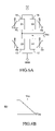
- FIG. 1 is a plan view showing an embodiment of a magnetic sensor (N-type) according to the present invention
- FIG. 2 is a plan view showing an embodiment of another magnetic sensor (S-type) according to the present invention.
- FIG. 3A is an enlarged schematic plan view showing a first X-axis GMR element shown in FIG. 1 ;
- FIG. 3B is a schematic sectional view of the first X-axis GMR element taken along line 1 — 1 of FIG. 3A ;
- FIG. 4 is a view showing the film configuration (configuration of synthetic spin valve film SAF) of the first X-axis GMR element shown in FIG. 3 ;
- FIG. 5 is a graph showing a variation in resistance of the first X-axis GMR element shown in FIG. 1 as represented by the solid line in the presence of a magnetic field that varies in the direction of the X-axis, and a variation in the resistance as represented by the broken line in the presence of a magnetic field that varies in the direction of the Y-axis;
- FIG. 6A is an equivalent circuit diagram of an X-axis magnetic sensor included in the magnetic sensor shown in FIG. 1 ;
- FIG. 6B is a graph showing a variation in output of the X-axis magnetic sensor of FIG. 6A in the presence of a magnetic field that varies in the direction of the X-axis;
- FIG. 7 is a plan view showing a magnet array used for pinning the magnetization directions of pinned layers of the magnetic sensors shown in FIGS. 1 and 2 ;
- FIG. 8 is a partial, sectional view showing the magnet array of FIG. 7 ;
- FIG. 9 is a plan view showing a yoke of the magnet array of FIG. 7 ;
- FIG. 10 is an enlarged partial plan view showing the yoke of FIG. 9 ;
- FIG. 11 is a sectional view of the yoke taken along line 2 — 2 of FIG. 10 ;
- FIG. 12 is a plan view showing a through hole formed in the yoke of FIG. 9 ;
- FIG. 13 is a partial, sectional view showing an array substrate of the magnet array of FIG. 7 ;
- FIG. 14 is a plan view showing the array substrate of the magnet array of FIG. 7 ;
- FIG. 15 is a sectional view showing a thin plate used to form the array substrate of FIG. 13 ;
- FIG. 16 is a view showing a step in manufacture of the magnet array of FIG. 7 ;
- FIG. 17 is a view showing another step in manufacture of the magnet array of FIG. 7 ;
- FIG. 18 is a view showing another step in manufacture of the magnet array of FIG. 7 ;
- FIG. 19 is a view showing another step in manufacture of the magnet array of FIG. 7 ;
- FIG. 20 is a partial, sectional view showing the magnet array of FIG. 7 for the purpose of explaining magnetic fields generated by the magnet array;
- FIG. 21 is a plan view showing the magnet array of FIG. 7 for the purpose of explaining magnetic fields generated by the magnet array;
- FIG. 22 is a partial plan view showing a wafer from which the magnetic sensors of FIGS. 1 and 2 are manufactured;
- FIG. 23 is a partial, sectional view showing the magnet array and the wafer, representing a method for pinning magnetizations of pinned layers of GMR elements of the magnetic sensors of FIGS. 1 and 2 in respectively fixed directions;
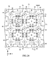
- FIG. 24 is a conceptual view showing the method for pinning magnetizations of pinned layers of GMR elements of the magnetic sensors of FIGS. 1 and 2 in respectively fixed directions;
- FIG. 25 is a graph showing the results of study on the relation between an annealing temperature and an exchange-coupling magnetic field with respect to a conventional spin valve film, and a synthetic spin valve film manufactured by the method of the present invention
- FIG. 26 is a graph showing the results of study on the relation between an annealing temperature and MR ratio with respect to the conventional spin valve film, and the synthetic spin valve film manufactured by the method of the present invention
- FIG. 27 is a conceptual view showing a positioning grid for magnetic sensors on a wafer
- FIG. 28 is a conceptual view showing a positioning grid for magnetic sensors on a wafer
- FIG. 29 is a graph showing output voltage characteristics of X-axis magnetic sensors located at various positions on the wafer of FIGS. 27 and 28 and manufactured by use of the magnet array of FIG. 7 ;
- FIG. 30 is a graph showing output voltage characteristics of X-axis magnetic sensors located at various positions on the wafer of FIGS. 27 and 28 and manufactured by use of a magnet array prepared by removing the yoke from the magnet array of FIG. 7 ;
- FIG. 31 is a graph showing output voltage characteristics of Y-axis magnetic sensors located at various positions on the wafer of FIGS. 27 and 28 and manufactured by use of the magnet array of FIG. 7 ;
- FIG. 32 is a graph showing output voltage characteristics of Y-axis magnetic sensors located at various positions on the wafer of FIGS. 27 and 28 and manufactured by use of the magnet array prepared by removing the yoke from the magnet array of FIG. 7 ;
- FIG. 33 is a diagram showing sensitivities of X-axis magnetic sensors located at various positions on the wafer of FIGS. 27 and 28 and manufactured by use of the magnet array of FIG. 7 ;
- FIG. 34 is a diagram showing sensitivities of X-axis magnetic sensors located at various positions on the wafer of FIGS. 27 and 28 and manufactured by use of a magnet array prepared by removing the yoke from the magnet array of FIG. 7 ;
- FIG. 35 is a diagram showing sensitivities of X-axis magnetic sensors located at various positions on the wafer of FIGS. 27 and 28 and manufactured by use of the magnet array of FIG. 7 ;
- FIG. 36 is a diagram showing sensitivities of X-axis magnetic sensors located at various positions on the wafer of FIGS. 27 and 28 and manufactured by use of the magnet array prepared by removing the yoke from the magnet array of FIG. 7 ;
- FIG. 37 is a diagram showing sensitivities of Y-axis magnetic sensors located at various positions on the wafer of FIGS. 27 and 28 and manufactured by use of the magnet array of FIG. 7 ;
- FIG. 38 is a diagram showing sensitivities of Y-axis magnetic sensors located at various positions on the wafer of FIGS. 27 and 28 and manufactured by use of the magnet array prepared by removing the yoke from the magnet array of FIG. 7 ;
- FIG. 39 is a diagram showing sensitivities of Y-axis magnetic sensors located at various positions on the wafer of FIGS. 27 and 28 and manufactured by use of the magnet array of FIG. 7 ;
- FIG. 40 is a diagram showing sensitivities of Y-axis magnetic sensors located at various positions on the wafer of FIGS. 27 and 28 and manufactured by use of the magnet array prepared by removing the yoke from the magnet array of FIG. 7 ;
- FIG. 41 is a plan view showing an embodiment of another magnetic sensor according to the present invention.
- FIG. 42 is a view showing the configuration of a conventional spin valve film
- FIG. 43 is a graph showing a variation in output of the magnetic sensor of FIG. 41 as observed after a strong magnetic field is applied thereto.
- FIG. 44 is a graph showing a variation in output of a conventional magnetic sensor having an element arrangement similar to that of FIG. 41 and employing the spin valve film of FIG. 42 , as observed after a strong magnetic field is applied thereto.
- the magnetic sensor is classified into an N-type magnetic sensor 10 shown in FIG. 1 and an S-type magnetic sensor 30 shown in FIG. 2 .
- the N-type and S-type magnetic sensors 10 and 30 are manufactured by manufacturing methods to be described later.
- the N-type magnetic sensor 10 and the S-type magnetic sensor 30 assume substantially the same shape and configuration except for the fixed magnetization direction of a pinned layer as represented by the black solid arrow of FIGS. 1 and 2 and the magnetization direction of a free layer in an initial state (a state in which an external magnetic field is absent) as represented by the inline arrow of FIGS. 1 and 2 . Therefore, the N-type magnetic sensor 10 will be mainly discussed below.
- the magnetic sensor 10 includes a single substrate (monolithic chip) 10 a and eight GMR elements 11 to 14 and 21 to 24 formed on (or above, over) the substrate 10 a .
- the substrate 10 a is made of quartz glass.
- the substrate 10 a is a thin plate that, as viewed in plane, assumes a rectangular shape (substantially square shape) having sides extending along mutually orthogonal X-axis and Y-axis and that has a small thickness along a Z-axis perpendicular to the X- and Y-axes.
- the GMR elements 11 to 14 and 21 to 24 have substantially the same structure, except for arrangement on the substrate 10 a . Therefore, the structure of the first X-axis GMR element 11 will be representatively described.
- the first X-axis GMR element 11 includes a plurality of narrow strip portions 11 a extending in the Y-axis and a plurality of bias magnet films 11 b formed under longitudinally opposite end portions (opposite end portions with respect to the Y-axis) of the narrow strip portions 11 a.
- the narrow strip portions 11 a are formed of a synthetic spin valve film SAF, which constitutes a magnetoresistance element having a multifilm laminated fixed layer.
- the bias magnet films 11 b are made of a hard ferromagnetic material, such as CoCrPt, having high coercive force and high remanence ratio and are magnetized to become permanent magnet films.
- the narrow strip portions 11 a are magnetically coupled to the bias magnet films 11 b at the upper surfaces of the bias magnet films 11 b.
- the synthetic spin valve film SAF of the first X-axis GMR element 11 is shown in FIG. 4 .
- the synthetic spin valve film SAF of the first X-axis GMR element 11 includes a dielectric layer 10 b (including a wiring layer(s)) formed on the substrate 10 a ; a free layer F formed on the dielectric layer 10 b ; a spacer layer S formed on the free layer F; a fixed layer P formed on the spacer layer S; and a capping layer C formed on the fixed layer P.
- Elements for the magnetic sensor 10 such as transistors and memories etc., are formed in or on the substrate 10 a .
- Wiring layers are included in the dielectric layer 10 b .
- the wiring layers connect the elements, pads and the GMR elements etc., to form the sensor 10 .
- the pads connect the magnetic sensor 10 with external equipment via Au wires bonded to the upper surfaces of the pads.
- the wiring layers may be called conductor lines.
- the substrate 10 a and the dielectric layer 10 b taken together, may be called a “substrate,” since the GMR elements 11 to 14 and 21 to 24 are formed thereon.
- the magnetization direction of the free layer F varies in accordance with the direction of an external magnetic field.
- the free layer F includes a CoZrNb amorphous magnetic layer 11 - 1 formed on the substrate (dielectric layer 10 b ) and having a thickness of 8 nm (80 angstroms); an NiFe magnetic layer 11 - 2 formed on the CoZrNb amorphous magnetic layer 11 - 1 and having a thickness of 3.3 nm (33 angstroms); and a CoFe layer 11 - 3 formed on the NiFe magnetic layer 11 - 2 and having a thickness of about 1 nm to 3 nm (10 angstroms to 30 angstroms).
- the CoZrNb amorphous magnetic layer 11 - 1 and the NiFe magnetic layer 11 - 2 constitute a soft ferromagnetic film.
- the CoFe layer 11 - 3 prevents diffusion of Ni from the NiFe layer 11 - 2 and diffusion of Cu from a Cu layer 11 - 4 of the spacer layer S.
- the spacer layer S is an electrically conductive film made of Cu and having a thickness of 2.4 nm (24 angstroms).
- the fixed layer (magnetization-fixed layer or pin layer) P includes a first ferromagnetic film 11 - 5 made of CoFe and having a thickness of 2.5 nm (25 angstroms); an exchange-coupling film 11 - 6 laminated on the first ferromagnetic film 11 - 5 , made of Ru, and having a thickness of 0.8 nm to 0.9 nm (8 angstroms to 9 angstroms); a second ferromagnetic film 11 - 7 laminated on the exchange-coupling film 11 - 6 , made of CoFe, and having a thickness of 2.2 nm (22 angstroms); and an exchange bias film (antiferromagnetic film) 11 - 8 laminated on the second ferromagnetic film 11 - 7 , having a thickness of 24 nm (240 angstroms), and made of a PtMn alloy that contains Pt in an amount of 45 mol % to 55 mol %.
- the exchange-coupling film 11 - 6 is sandwiched between the first ferromagnetic film 11 - 5 and the second ferromagnetic film 11 - 7 .
- the first ferromagnetic film 11 - 5 , the exchange-coupling film 11 - 6 , and the second ferromagnetic film 11 - 7 constitute a pinned layer whose magnetization is pinned in a fixed direction so that the magnetization direction does not vary with a variation in an external magnetic field.
- the exchange bias film 11 - 8 is a pinning layer for pinning the magnetization of the pinned layer in a fixed direction.
- the exchange bias film 11 - 8 is exchange-coupled to the second ferromagnetic film 11 - 7 , thereby pinning the magnetization (magnetization vector) of the second ferromagnetic film 11 - 7 in a fixed direction.
- the first ferromagnetic film 11 - 5 and the second ferromagnetic film 11 - 7 are exchange-coupled to each other via the exchange-coupling film 11 - 6 .
- the magnetization of the first ferromagnetic film 11 - 5 is pinned in a fixed direction.
- the magnetization direction of the first ferromagnetic film 11 - 5 and the magnetization direction of the second ferromagnetic film 11 - 7 are antiparallel with each other.
- FIG. 1 when ordering heat treatment is performed while the direction of a magnetic field is set to the positive direction of the X-axis, the magnetization of the first ferromagnetic film 11 - 5 of the first X-axis GMR element 11 is pinned in the negative direction of the X-axis.
- the magnetization direction of the first ferromagnetic film 11 - 5 is a direction in which the magnetization of the pinned layer of the first X-axis GMR element is pinned.
- the capping layer C has a thickness of 1.5 nm (15 angstroms) and is made of titanium (Ti) or tantalum (Ta).
- the bias magnet films 11 b shown in FIGS. 3A and 3B apply a bias magnetic field to the free layer F in a longitudinal direction of the free layer F in order to maintain uniaxial anisotropy of the free layer F.
- the bias magnet films 11 b apply a bias magnetic field in the negative direction of the Y-axis.
- the thus-configured first X-axis GMR element 11 exhibits the following characteristics. As represented by the solid line in FIG. 5 , in the presence of an external magnetic field that varies along the X-axis, the resistance of the first X-axis GMR element 11 varies substantially in proportion to the external magnetic field within the range of ⁇ Hc to +Hc. As represented by the broken line in FIG. 5 , the resistance of the first X-axis GMR is substantially constant in the presence of an external magnetic field that varies along the Y-axis. In other words, the first X-axis GMR element 11 detects a magnetic field in the direction in which the magnetization of the pinned layer is pinned.
- the first X-axis GMR element 11 is formed on the substrate 10 a at a position located on a side toward the negative direction of the Y-axis with respect to a central portion of the substrate 10 a and in the vicinity of an edge portion of the substrate 10 a with respect to the negative direction of the X-axis.
- the magnetization of the pinned layer of the first X-axis GMR element 11 is pinned in the negative direction of the X-axis.
- the second X-axis GMR element 12 is formed on the substrate 10 a at a position located on a side toward the positive direction of the Y-axis with respect to a central portion of the substrate 10 a and in the vicinity of an edge portion of the substrate 10 a with respect to the negative direction of the X-axis; and the magnetization of the pinned layer of the second X-axis GMR element 12 is pinned in the negative direction of the X-axis.
- the third X-axis GMR element 13 is formed on the substrate 10 a at a position located on a side toward the positive direction of the Y-axis with respect to a central portion of the substrate 10 a and in the vicinity of an edge portion of the substrate 10 a with respect to the positive direction of the X-axis; and the magnetization of the pinned layer of the third X-axis GMR element 13 is pinned in the positive direction of the X-axis.
- the fourth X-axis GMR element 14 is formed on the substrate 10 a at a position located on a side toward the negative direction of the Y-axis with respect to a central portion of the substrate 10 a and in the vicinity of an edge portion of the substrate 10 a with respect to the positive direction of the X-axis; and the magnetization of the pinned layer of the fourth X-axis GMR element 14 is pinned in the positive direction of the X-axis.
- the first Y-axis GMR element 21 is formed on the substrate 10 a at a position located on a side toward the negative direction of the X-axis with respect to a central portion of the substrate 10 a and in the vicinity of an edge portion of the substrate 10 a with respect to the positive direction of the Y-axis; and the magnetization of the pinned layer of the first Y-axis GMR element 21 is pinned in the positive direction of the Y-axis.
- the second Y-axis GMR element 22 is formed on the substrate 10 a at a position located on a side toward the positive direction of the X-axis with respect to a central portion of the substrate 10 a and in the vicinity of an edge portion of the substrate 10 a with respect to the positive direction of the Y-axis; and the magnetization of the pinned layer of the second Y-axis GMR element 22 is pinned in the positive direction of the Y-axis.
- the third Y-axis GMR element 23 is formed on the substrate 10 a at a position located on a side toward the positive direction of the X-axis with respect to a central portion of the substrate 10 a and in the vicinity of an edge portion of the substrate 10 a with respect to the negative direction of the Y-axis; and the magnetization of the pinned layer of the third Y-axis GMR element 23 is pinned in the negative direction of the Y-axis.
- the fourth Y-axis GMR element 24 is formed on the substrate 10 a at a position located on a side toward the negative direction of the X-axis with respect to a central portion of the substrate 10 a and in the vicinity of an edge portion of the substrate 10 a with respect to the negative direction of the Y-axis; and the magnetization of the pinned layer of the fourth Y-axis GMR element 24 is pinned in the negative direction of the Y-axis.
- an X-axis magnetic sensor (magnetic sensor for detecting a magnetic field in the X-direction) including the GMR elements 11 to 14
- a Y-axis magnetic sensor (magnetic sensor for detecting a magnetic field in the Y-direction) including the GMR elements 21 to 24 , will be described.
- the X-axis magnetic sensor is configured by full bridge connection of the first to fourth X-axis GMR elements 11 to 14 via unillustrated conductors.
- graphs which accompany the first to fourth X-axis GMR elements 11 to 14 show characteristics (variation in resistance R with external magnetic field) of the GMR elements adjacent thereto.
- Hx appearing in the graphs represent an external magnetic field whose intensity varies along the X-axis (X-axis component of an external magnetic field).
- connection point of the first X-axis GMR element 11 and the fourth X-axis GMR element 14 and the connection point of the second X-axis GMR element 12 and the third X-axis GMR element 13 are connected to the positive pole and the negative pole (ground), respectively, of an unillustrated constant-voltage source, whereby the potential +V (5 V in the present embodiment) and the potential ⁇ V (0 V in the present embodiment) are applied to the respective connection points.
- the potential difference V 0x between the connection point of the first X-axis GMR element 11 and the third X-axis GMR element 13 and the connection point of the fourth X-axis GMR element 14 and the second X-axis GMR element 12 is obtained as a sensor output.
- the X-axis magnetic sensor outputs the voltage V 0x , which is substantially in proportion to an external magnetic field Hx that varies along the X-axis and which decreases as the external magnetic field Hx increases.
- the Y-axis magnetic sensor is configured by full bridge connection of the first to fourth Y-axis GMR elements 21 to 24 via unillustrated conductors.
- the Y-axis magnetic sensor outputs the voltage V 0y , which is substantially in proportion to an external magnetic field Hy that varies along the Y-axis and which decreases as the external magnetic field Hy increases.
- the N-type magnetic sensor 10 is configured as described above.
- the S-type magnetic sensor 30 includes GMR elements 31 to 34 and 41 to 44 .
- the magnetic sensor 30 is configured in a manner similar to the magnetic sensor 10 and is composed of an X-axis magnetic sensor and a Y-axis magnetic sensor.
- the X-axis magnetic sensor of the magnetic sensor 30 is configured by full bridge connection of the first to fourth X-axis GMR elements 31 to 34 via unillustrated conductors.
- the X-axis magnetic sensor of the magnetic sensor 30 outputs a voltage V 0x , which is substantially in proportion to the external magnetic field Hx and which increases as the external magnetic field Hx increases.
- the Y-axis magnetic sensor of the magnetic sensor 30 is configured by full bridge connection of the first to fourth Y-axis GMR elements 41 to 44 via unillustrated conductors.
- the Y-axis magnetic sensor of the magnetic sensor 30 outputs a voltage V 0y , which is substantially in proportion to the external magnetic field Hy and which increases as the external magnetic field Hy increases.
- the magnet array 50 is used for pinning the magnetizations of pinned layers of the fixed layers P of the magnetic sensors 10 and 30 in respectively fixed directions.
- the magnet array 50 includes a yoke (yoke plate) 60 , an array substrate 70 , and a plurality of permanent magnets (permanent bar magnets) 80 .
- the yoke 60 is shown in FIGS. 9 to 11 .
- FIG. 9 is a plan view of the yoke 60 ;
- FIG. 10 is an enlarged partial view of FIG. 9 ;
- FIG. 11 is a sectional view of the yoke 60 taken along line 2 — 2 of FIG. 10 .
- the yoke 60 is a thin plate member made of a magnetic material having a magnetic permeability higher than that of the air, such as 42 alloy (Fe-42 Ni alloy which contains Ni in an amount of 42 wt. %).
- the yoke 60 may be made of a high-saturation, high-magnetic-permeability material, such as Permalloy or silicon steel (sheet).
- the yoke 60 assumes a rectangular shape as viewed in plane. In the present embodiment, the yoke 60 has a thickness of 0.15 mm.
- the yoke 60 includes a plurality of through holes 61 and a plurality of openings (magnetic-flux control holes) 62 . As shown in the enlarged view of FIG. 12 , each of the through holes 61 includes a single square portion 61 a , four rectangular portions 61 b , and four marginal portions (circular arc portions or R portions) 61 c.
- the square portion 61 a has a square shape as viewed in plane.
- Each of the rectangular portions 61 b has a rectangular shape that is formed along a central portion of a side of the square portion 61 a in such a manner as to expand to the exterior of the square portion 61 a and has the central portion as its long side (i.e., the central portion forms one long side of the rectangular shape).
- Each of the marginal portions 61 c expands to the exterior of the square portion 61 a from a corresponding corner portion of the square portion 61 a . More specifically, each of the marginal portions 61 c assumes the shape of a circular arc whose center RP is located on a diagonal line CR of the square portion 61 a.
- the plurality of through holes 61 are arranged in a tetragonal lattice array.
- the centroid of each through hole 61 coincides with a lattice point SP of the tetragonal lattice shown in FIG. 10 .
- One side of the square portion 61 a of a certain through hole 61 is in parallel with one side of the square portion 61 a of an adjacent through hole 61 .
- One side of the square portion 61 a of a certain through hole 61 is aligned with one side of the square portion 61 a of another through hole 61 formed in the same column or row as the certain through hole 61 .
- one side of the rectangular portion 61 b of a certain through hole 61 is aligned with one side of the rectangular portion 61 b of another through hole 61 formed in the same column or row as the certain through hole 61 .
- the openings 62 are formed at positions where centroids CP of squares formed by connecting lattice points SP of the tetragonal lattice are located within the corresponding opening 62 . That is, each of openings 62 is formed to surround a centroid CP of square formed by connecting adjacent lattice points SP of the tetragonal lattice. More specifically, as viewed in plane, each of the openings 62 is a circular through hole whose center is located at the centroid CP.
- the array substrate 70 shown in FIGS. 13 and 14 is formed from a thin plate 70 a of a magnetic material (e.g., Permalloy such as 42 alloy) shown in FIG. 15 .
- the array substrate 70 has a rectangular shape substantially identical in shape with the yoke 60 .
- the array substrate 70 includes a plurality of grooves 70 b .
- the plurality of grooves 70 b are located at the same positions as the corresponding square portions 61 a of the through holes 61 of the yoke 60 .
- Each of the grooves 70 b has a square shape substantially identical in shape with the square portion 61 a of the through hole 61 .
- Each of the permanent bar magnets 80 assumes the shape of a rectangular parallelepiped.
- the cross section of the rectangular parallelepiped cut by a plane perpendicular to one center axis of the rectangular parallelepiped (e.g., relatively longer axis of the rectangular parallelepiped) has a square shape substantially identical in shape with the square portion 61 a of the through hole 61 and with the groove 70 b of the array substrate 70 .
- Each of the permanent bar magnets 80 has magnetic poles generated in the vicinity of its corresponding opposite end surfaces, which have the square shape.
- the plurality of permanent bar magnets 80 have substantially the same magnetic charge.
- the permanent bar magnets 80 are inserted into the corresponding grooves 70 b of the array substrate 70 and through the corresponding square portions 61 a of the yoke 60 to thereby be held in place.
- the permanent bar magnets 80 are arranged such that two adjacent, closest permanent bar magnets 80 differ in polarity between magnetic poles generated on their end surfaces (i.e., the magnetic poles generated on the end surfaces of two adjacent, closest permanent magnets differ in polarity.).
- the magnet array 50 includes a plurality of permanent bar magnets 80 and a thin-plate yoke 60 made of a magnetic material.
- Each permanent bar magnet 80 has the shape of a substantially rectangular parallelepiped.
- the rectangular parallelepiped has a cross section in a substantially square shape taken perpendicular to its axis.
- Each permanent bar magnet 80 has magnetic poles generated on its corresponding opposite end surfaces having the substantially square shape perpendicular to the axis.
- the plurality of permanent bar magnets 80 are arranged in such a manner that the centroid of each of substantially square end surfaces thereof coincides with a lattice point SP of a tetragonal lattice and that the permanent bar magnets 80 arranged on the same lattice line of the tetragonal lattice are such that one side of the end surface of a certain permanent bar magnet 80 is substantially aligned with one side of the end surface of another permanent bar magnet 80 . Furthermore, the plurality of permanent bar magnets 80 are arranged in such a manner that the end surfaces thereof are present substantially on the same plane and that magnetic poles generated on the end surfaces of two adjacent, closest permanent bar magnets 80 differ in polarity.
- the yoke 60 has a plurality of through holes 61 arranged in substantially the same manner as the arranged permanent bar magnets 80 .
- Each through hole 61 includes a square portion 61 a having a shape substantially identical with the substantially square shape of the cross section of the permanent bar magnet 80 , and rectangular portions 61 b each being formed along a central portion of a side of the square portion 61 a and having the central portion as its long side.
- the plurality of permanent bar magnets 80 are inserted through the corresponding square portions 61 a of the plurality of through holes 61 .
- a plane in which the end surfaces of the permanent bar magnets 80 are present is located between the upper surface and the lower surface of the yoke 60 .
- a method for manufacturing the magnet array 50 will be described.
- a plate used to form the yoke 60 is prepared. Etching is performed on the plate to thereby form the through holes 61 and the openings 62 .
- the thin plate 70 a (see FIG. 15 ) used to form the array substrate 70 is prepared. Etching (half etching) is performed on the thin plate 70 a to thereby form the grooves 70 b (see FIGS. 13 and 14 ).
- prism-like (prismatic) spacers 90 made of glass are arranged on the array substrate 70 .
- Each of the spacers 90 is disposed on the array substrate 70 between two adjacent parallel lines of the grooves 70 b .
- the length of the spacer 90 in the Z-axis is shorter than the length between the opposite end surfaces of the permanent bar magnet 80 , on which magnetic poles are formed.
- the yoke 60 is placed on the spacers 90 .
- the yoke 60 is disposed in such a manner that, as viewed in plane, the grooves 70 b of the array substrate 70 are aligned with the corresponding square portions 61 a of the through holes 61 of the yoke 60 .
- a positioning mark (alignment mark) may be provided on the yoke 60 and on the array substrate 70 . Note that, in FIG. 16 , the marginal portions 61 c are omitted.
- the permanent bar magnets 80 are inserted through the corresponding through holes 61 .
- the inserting work is performed in such a manner that the polarized first-side end surfaces of the permanent bar magnets 80 abut the corresponding bottom surfaces of the grooves 70 b of the array substrate 70 .
- the polarized second-side end surfaces (hereinafter may be referred as “upper surfaces” for convenience sake) of the permanent bar magnets 80 are present in substantially the same plane (on the same plane).
- the permanent bar magnets 80 are arranged such that the magnetic poles generated on the end surfaces of two adjacent, closest permanent magnets 80 differ in polarity, as viewed in the plane that includes the upper surfaces of the permanent bar magnets 80 .
- the permanent bar magnets 80 are arranged as shown in FIG. 18 . In this state, movement of the permanent bar magnets 80 in the X- and Y-axis directions is prevented, since the permanent bar magnets 80 are inserted into the grooves 70 b and the square portions 61 a of the through holes 61 of the yoke 60 .
- the yoke 60 is raised (in the positive direction of the Z-axis) by means of utilizing the openings 62 . Specifically, the yoke 60 is raised while being held at the two openings 62 by use of tweezers. This raising work is repeatedly performed by utilizing other openings 62 so as to gradually raise the entire yoke 60 .
- the height of the yoke 60 (the distance between the array substrate 70 and the yoke 60 ) is adjusted in such a manner that a plane defined by the upper surfaces of the permanent bar magnets 80 (the polarized second-side end surfaces of the permanent bar magnets 80 ) is located between an upper surface 60 up and a lower surface 60 dn of the yoke 60 .
- the yoke 60 is raised such that the upper surfaces of the permanent bar magnets 80 are located within the range of the thickness of the yoke 60 .
- the upper surface 60 up of the yoke 60 and the plane defined by the upper surfaces of the permanent bar magnets 80 may be present in the same plane.
- a rightward magnetic field is generated from a certain N-pole toward an S-pole located on the right side of the N-pole; an upward magnetic field is generated from the N-pole toward an S-pole located on the upper side of the N-pole; a leftward magnetic field is generated from the N-pole toward an S-pole located on the left side of the N-pole; and a downward magnetic field is generated from the N-pole toward an S-pole located on the lower side of the N-pole.
- a leftward magnetic field is generated toward a certain S-pole from an N-pole located on the right side of the S-pole; a downward magnetic field is generated toward the S-pole from an N-pole located on the upper side of the S-pole; a rightward magnetic field is generated toward the S-pole from an N-pole located on the left side of the S-pole; and an upward magnetic field is generated toward the S-pole from an N-pole located on the lower side of the S-pole.
- Lines of magnetic force associated with the magnetic fields pass along the yoke 60 , through the rectangular portions 61 b of the yoke 60 , and immediately above the rectangular portions 61 b .
- the magnet array 50 has the openings 62 .
- the openings 62 are formed at positions where the centroids CP of squares formed by connecting lattice points SP of the tetragonal lattice; i.e., by connecting the centroids of the through holes 61 (square portions 61 a ) of the yoke 60 , are located. That is, each of openings 62 is formed so as to surround a centroid CP of square formed by connecting adjacent lattice points SP of the tetragonal lattice.
- the positions where the openings 62 are formed are where lines of magnetic force extending (generating) from magnetic poles of the permanent bar magnets 80 intersect, with resultant instability in magnetic fields. Forming the openings 62 at the positions prevents intersection of lines of magnetic force, thereby eliminating instability in magnetic fields.
- stable, strong, uniform magnetic fields can be locally generated in the rectangular portions 61 b and at portions immediately above the rectangular portions 61 b.
- the dielectric layer 10 b shown in FIGS. 3(B) and 4 is formed on a wafer (quartz glass or Si substrate) 10 a 1 shown in FIG. 22 .
- a wafer quartz glass or Si substrate
- predetermined wirings, LSIs, and unillustrated coils for initializing the free layers F are formed.
- the wafer 10 a 1 is cut at a later step along cutting lines CL represented by the broken line of FIG. 22 , thereby yielding the substrates 10 a and 30 a.
- a plurality of films (element films) M to become the GMR elements 11 to 14 , 21 to 24 , 31 to 34 , and 41 to 44 are formed.
- films to become the bias magnet films 11 b are formed.
- films to become the synthetic spin valve films SAF each film including a film to become the fixed layer, a film to become the spacer layer, and a film to become the free layer are formed on the films 11 b .
- This film deposition process is performed by use of an ultra-high vacuum apparatus in such a manner that component films are continuously laminated with accurately controlled respective thicknesses.
- the films are patterned to form a plurality of island-like films M, each of which has the same shape as the narrow strip portions 11 a .
- the films M are to become island-like GMR elements.
- the films M are formed on the quartz glass 10 a 1 in such a manner that, when the quartz glass 10 a 1 is cut at a later step along the cutting lines CL represented by the broken line of FIG. 22 to thereby form the magnetic sensors 10 and 30 shown in FIGS. 1 and 2 , the films M are arranged at the positions of the GMR elements 11 to 14 , 21 to 24 , 31 to 34 , and 41 to 44 .
- the at least two element films M are disposed on the substrate (wafer 10 a 1 ).
- the at least two element films M are formed such that, while one element film M is disposed at a position corresponding to (i.e., disposed inside of) a certain rectangular portion 61 b formed along a certain side of a certain square portion 61 a of the magnet array 50 , the other element film M is disposed at a position corresponding to (i.e., disposed inside of) another rectangular portion 61 b formed along a side of the square portion 61 a adjacent to the former side of the square portion 61 a.
- the wafer 10 a 1 on which the films M are formed, and the magnet array 50 are arranged as shown in FIG. 23 .
- the side of the wafer 10 a 1 on which the films M are formed is brought into contact with the upper surface 60 up of the yoke 60 .
- the wafer 10 a 1 and the magnet array 50 are arranged in such a relation that each of the intersection points CP of the cutting lines CL corresponding to sides of the magnetic sensors 10 and 30 , coincides with the centroid of a group of four adjacent permanent bar magnets 80 .
- magnetic fields are applied to the films M perpendicularly to the longitudinal direction of the narrow strip portions 11 a of the films M.
- the wafer 10 a 1 and the magnet array 50 which are arranged in the above-mentioned relation, are heated to a temperature of 250° C. to 280° C. (preferably 270° C.) in a vacuum and are held at the temperature for about three hours.
- the wafer 10 a 1 is disposed in the proximity of the magnet array 50 such that, as viewed in plane, while one element film M is disposed at a position corresponding to (i.e., disposed inside of) a certain rectangular portion 61 b formed along a certain side of a certain square portion 61 a of the magnet array 50 , another element film M is disposed at a position corresponding to (i.e., disposed inside of) another rectangular portion 61 b formed along a side of the square portion 61 a adjacent to the former side of the square portion 61 a , magnetic fields generated in the vicinity of (at portions immediately above) the rectangular portions 61 b of the magnet array 50 are applied to the element films M, and the wafer 10 a 1 having the element films M are held at high temperature, whereby the magnetizations of films (pinned layers) to become the fixed layers of the plurality of element films M are simultaneously pinned in respectively fixed directions.
- the wafer 10 a 1 is allowed to stand without application of heat until the wafer 10 a 1 cools to the room temperature. Then, the wafer 10 a 1 is unloaded from the vacuum apparatus. Wirings for connecting the films M, and the like are formed. Finally, the wafer 10 a 1 is cut along the cutting lines CL shown in FIGS. 22 and 24 . Thus, a large number of monolithic (single-chip) magnetic sensors 10 and 30 shown in FIGS. 1 and 2 are manufactured at a time.
- the present embodiment performs the heat treatment process in which strong magnetic fields are locally generated by use of the magnet array 50 and are used for pinning the magnetization directions of pinned layers of the synthetic spin valve films SAF.
- the magnet array 50 includes the yoke 60 in which the rectangular portions 61 b are formed and function as air gaps. Accordingly, by use of the magnet array 50 , strong, uniform magnetic fields can be generated in spaces in the vicinity of the rectangular portions 61 b , so that magnetizations of pinned layers of the synthetic spin valve films SAF can be reliably pinned in respectively fixed directions.
- the openings 62 are formed at portions where lines of magnetic force extending from magnetic poles would otherwise intersect with resultant instability in magnetic fields. As a result, directional properties of lines of magnetic force become stable, and thus magnetic fields in the vicinity of the openings 62 can be stabilized to a greater extent. Also, the openings 62 are utilized in adjusting the distance between the yoke 60 and the array substrate 70 of the magnetic array 50 (height of the yoke 60 ).
- the magnet array 60 can generate mutually intersecting (orthogonal), strong uniform magnetic fields in adjacent regions (at portions immediately above the adjacent rectangular portions 61 b ). Accordingly, there can be readily manufactured a biaxial magnetic sensor that employs the synthetic spin valve films SAF having excellent heat resistance, excellent resistance to strong magnetic fields, and good temperature characteristics.
- each of the through holes 61 has marginal portions 61 c which are formed at corresponding corners of the square portion 61 a in such a manner as to expand diagonally outward. Accordingly, even when, in the process of etching the through holes 61 , corner portions of the square portions 61 a are insufficiently etched, the permanent bar magnets 80 can be reliably inserted through the corresponding through holes 61 .
- the graph of FIG. 25 shows the results of study on the relation between an annealing temperature TA and an exchange-coupling magnetic field Hua with respect to the conventional spin valve film SV and the above-manufactured synthetic spin valve film SAF.
- the annealing temperature TA is a predetermined temperature at which the GMR element is held for annealing. More specifically, the GMR element is annealed as follows: while a magnetic field of a predetermined intensity ( 1000 e in the example of FIG. 25 ) is applied to the GMR element in a direction opposite the pinned magnetization direction of the pinned layer of the GMR element, the GMR element is held at the annealing temperature TA through application of heat; subsequently, the GMR element is allowed to cool to the room temperature.
- a magnetic field of a predetermined intensity 1000 e in the example of FIG. 25
- the exchange-coupling magnetic field Hua is a magnetic field H that causes the following: when the magnetic field H is applied to the annealed GMR element at the room temperature in a direction opposite the pinned magnetization direction of the pinned layer of the annealed GMR element, the magnetization direction of the pinned layer changes from the initially fixed magnetization direction.
- the synthetic spin valve film SAF manufactured by the method of the present embodiment exhibits a value of the exchange-coupling magnetic field Hua higher than that of the conventional spin valve film SV and maintains the exchange-coupling magnetic field Hua at high level until a higher annealing temperature is reached as compared with the conventional spin valve film SV.
- the graph of FIG. 26 shows the results of study on the relation between the annealing temperature TA and an MR ratio with respect to the conventional spin valve film SV and the above-manufactured synthetic spin valve film SAF.
- the synthetic spin valve film SAF manufactured by the method of the present embodiment exhibits a value of the MR ratio higher than that of the conventional spin valve film SV and maintains the MR ratio at high level until a higher annealing temperature is reached as compared with the conventional spin valve film SV. That is, the synthetic spin valve film SAF manufactured by the method of the present embodiment exhibits higher heat resistance as compared with the conventional spin valve film SV.
- the magnetic sensors 10 and 30 having consistent characteristics can be obtained.
- FIGS. 27 and 28 are schematic views showing the locations on a wafer of the magnetic sensors used for experiments.
- FIG. 27 shows a wafer on which a large number of the films M are formed.
- FIG. 28 is an enlarged view of one of square portions shown in FIG. 27 .
- FIG. 29 shows characteristics (variation of output voltage with external magnetic field) of X-axis magnetic sensors located at a chip position (X-position, Y-position) of (7, 7) shown in FIG. 28 in a shot position (X-position, Y-position) of (3, 3), (3, 5), . . . , (7, 5), and (7, 7) shown in FIG. 27 .
- the X-axis magnetic sensors are manufactured by use of the magnet array 50 , which includes the yoke 60 .
- FIG. 30 shows characteristics of X-axis magnetic sensors located at a chip position (X-position, Y-position) of (7, 5) shown in FIG. 28 in a shot position (X-position, Y-position) of (3, 3), (3, 5), . . . , (7, 5), and (7, 7) shown in FIG. 27 .
- the X-axis magnetic sensors are manufactured by use of a magnet array prepared by removing the yoke 60 from the magnet array 50 .
- the X-axis magnetic sensor formed in the shot position of (7, 3) exhibits an inverted characteristic curve as compared with normal X-axis magnetic sensors; and the X-axis magnetic sensor formed in the shot position of (3, 3) exhibits a poor output characteristic.
- the X-axis magnetic sensors manufactured by use of the magnet array 50 which includes the yoke 60 , exhibit a consistent output characteristic, irrespective of the shot position.
- FIG. 31 shows characteristics of Y-axis magnetic sensors located at a chip position (X-position, Y-position) of (7, 8) shown in FIG. 28 in a shot position (X-position, Y-position) of (3, 3), (3, 5), . . . , (7, 5), and (7, 7) shown in FIG. 27 .
- the Y-axis magnetic sensors are manufactured by use of the magnet array 50 , which includes the yoke 60 .
- FIG. 32 shows characteristics of Y-axis magnetic sensors located at a chip position (X-position, Y-position) of (7, 6) shown in FIG. 28 in a shot position (X-position, Y-position) of (3, 3), (3, 5), . . . , (7, 5), and (7, 7) shown in FIG. 27 .
- the Y-axis magnetic sensors are manufactured by use of a magnet array prepared by removing the yoke 60 from the magnet array 50 .
- the Y-axis magnetic sensor formed in the shot position of (7, 3) exhibits an inverted characteristic curve as compared with normal Y-axis magnetic sensors; and the Y-axis magnetic sensor formed in the shot position of (3, 3) exhibits a poor output characteristic.
- the Y-axis magnetic sensors manufactured by use of the magnet array 50 which includes the yoke 60 , exhibit a consistent output characteristic, irrespective of the shot position.
- FIG. 33 shows the sensitivity (variation of output voltage per unit magnetic field strength) of X-axis magnetic sensors located at a chip position of (7, 7) in the above-mentioned shot positions and manufactured by use of the magnet array 50 , which includes the yoke 60 .
- FIG. 34 shows the sensitivity of X-axis magnetic sensors located at a chip position of (7, 5) in the above-mentioned shot positions and manufactured by use of the magnet array prepared by removing the yoke 60 from the magnet array 50 .
- FIG. 35 shows the sensitivity of X-axis magnetic sensors located at a chip position of (7, 8) in the above-mentioned shot positions and manufactured by use of the magnet array 50 , which includes the yoke 60 .
- FIG. 36 shows the sensitivity of X-axis magnetic sensors located at a chip position of (7, 6) in the above-mentioned shot positions and manufactured by use of the magnet array prepared by removing the yoke 60 from the magnet array 50 .
- FIG. 37 shows the sensitivity of Y-axis magnetic sensors located at a chip position of (7, 7) in the above-mentioned shot positions and manufactured by use of the magnet array 50 , which includes the yoke 60 .
- FIG. 38 shows the sensitivity of Y-axis magnetic sensors located at a chip position of (7, 5) in the above-mentioned shot positions and manufactured by use of the magnet array prepared by removing the yoke 60 from the magnet array 50 .
- FIG. 39 shows the sensitivity of Y-axis magnetic sensors located at a chip position of (7, 8) in the above-mentioned shot positions and manufactured by use of the magnet array 50 , which includes the yoke 60 .
- FIG. 40 shows the sensitivity of Y-axis magnetic sensors located at a chip position of (7, 6) in the above-mentioned shot positions and manufactured by use of the magnet array prepared by removing the yoke 60 from the magnet array 50 .
- the magnetic sensors that were manufactured by use of the magnet array 50 exhibit good sensitivity.
- the magnetic sensors that were manufactured by use of the magnet array which does not have the yoke 60 include those whose sensitivity is poor. This indicates that a biaxial magnetic sensor manufactured by use of the magnet array 50 of the present invention exhibits excellent heat resistance and an excellent output characteristic.
- a magnetic sensor 100 including elements arranged as shown in FIG. 41 , each element including the synthetic spin valve film SAF, in a manner similar to that of the above-described embodiment. Also, there was manufactured a magnetic sensor 100 ′ (not shown) including elements arranged in a manner similar to that of the magnetic sensor 100 , each element including a conventional spin valve film (having the film configuration shown in FIG. 42 ).
- the magnetic sensor 100 includes GMR elements 111 to 114 and GMR elements 121 to 124 .
- the GMR elements 111 to 114 correspond to the GMR elements 11 to 14 , respectively, of the magnetic sensor 10 .
- the GMR elements 121 to 124 correspond to the GMR elements 21 to 24 , respectively, of the magnetic sensor 10 .
- FIG. 41 shows the arrangement of the GMR elements 111 to 114 and 121 to 124 , magnetization directions of pinned layers, and magnetization directions of free layers in the absence of an external magnetic field.
- a magnetic field having an intensity of 20, 40, 60, 80, and 100 (Oe) was applied to the magnetic sensor 100 and the conventional magnetic sensor 100 ′ in the positive and negative directions of the X-axis by use of a magnetic coil. Subsequently, the applied magnetic field was removed, and the magnetic sensors 100 and 100 ′ were examined for the output voltage of the X- and Y-axis magnetic sensors. The results are shown in FIGS. 43 and 44 . As is apparent from comparison between FIGS. 43 and 44 , the magnetic sensor 100 according to the present invention hardly exhibits a variation in output after a magnetic field is applied thereto (see FIG. 43 ). By contrast, the conventional magnetic sensor 100 ′ exhibits a very large variation in output after a magnetic field is applied thereto (see FIG. 44 ). This indicates that the magnetic sensor 100 according to the present invention is superior to the conventional magnetic sensor 100 ′ in resistance to strong magnetic field.
- the magnetic sensor is a sensor being formed in such a manner that a plurality of said magnetoresistance effect elements (e.g., GMR elements) are provided in a single plane on a single chip (substrate) having a generally square shape, said magnetoresistance effect elements are placed symmetrically with respect to center lines of said generally square chip, and the pinned layers of at least two of said plurality of magnetoresistance effect elements have the pinned magnetization directions that cross each other (i.e., the pinned magnetization directions cross each other with 90 degrees).
- GMR elements magnetoresistance effect elements
- the magnetic sensor 10 above includes four said magnetoresistance effect elements constructing a X-axis or a Y-axis magnetic sensor by full bridge connection of the four elements, said pinned magnetization directions of the pinned layers of the four elements being parallel each other.
- Embodiments of the present invention have been described with respect to a method for manufacturing a magnetic sensor, a magnet array, and a method for manufacturing the magnet array.
- the present invention is not limited thereto, but may be embodied in many other specific forms without departing from the scope of the invention.
- the films M are not necessarily patterned.
- the films M may be patterned after magnetizations of pinned layers are pinned in respectively fixed directions.
Landscapes
- Physics & Mathematics (AREA)
- Chemical & Material Sciences (AREA)
- Engineering & Computer Science (AREA)
- Nanotechnology (AREA)
- Condensed Matter Physics & Semiconductors (AREA)
- General Physics & Mathematics (AREA)
- Crystallography & Structural Chemistry (AREA)
- Hall/Mr Elements (AREA)
- Measuring Magnetic Variables (AREA)
- Measuring Instrument Details And Bridges, And Automatic Balancing Devices (AREA)
Applications Claiming Priority (2)
| Application Number | Priority Date | Filing Date | Title |
|---|---|---|---|
| JP2004-70927 | 2004-03-12 | ||
| JP2004070927A JP4557134B2 (ja) | 2004-03-12 | 2004-03-12 | 磁気センサの製造方法、同磁気センサの製造方法に使用されるマグネットアレイ及び同マグネットアレイの製造方法 |
Publications (2)
| Publication Number | Publication Date |
|---|---|
| US20050200449A1 US20050200449A1 (en) | 2005-09-15 |
| US7023310B2 true US7023310B2 (en) | 2006-04-04 |
Family
ID=34824631
Family Applications (1)
| Application Number | Title | Priority Date | Filing Date |
|---|---|---|---|
| US11/076,069 Expired - Fee Related US7023310B2 (en) | 2004-03-12 | 2005-03-10 | Method for manufacturing magnetic sensor, magnet array used in the method, and method for manufacturing the magnet array |
Country Status (7)
| Country | Link |
|---|---|
| US (1) | US7023310B2 (enExample) |
| EP (1) | EP1574870A3 (enExample) |
| JP (1) | JP4557134B2 (enExample) |
| KR (1) | KR100627212B1 (enExample) |
| CN (2) | CN2791885Y (enExample) |
| HK (1) | HK1080605B (enExample) |
| TW (1) | TWI293372B (enExample) |
Cited By (8)
| Publication number | Priority date | Publication date | Assignee | Title |
|---|---|---|---|---|
| US20070205766A1 (en) * | 2006-03-03 | 2007-09-06 | Futoyoshi Kou | Magnetoresistance effect element, substrate therefor and manufacturing method thereof |
| US20080024120A1 (en) * | 2006-07-26 | 2008-01-31 | Alps Electric Co., Ltd. | Magnetic sensor including bridge circuit having fixed resistance like structure of element |
| US20080297954A1 (en) * | 2007-04-19 | 2008-12-04 | Yamaha Corporation | Magnetic sensor and manufacturing method therefor |
| US20110121826A1 (en) * | 2008-05-08 | 2011-05-26 | Everspin Technologies, Inc. | Two-Axis Magnetic Field Sensor with Multiple Pinning Directions |
| EP2071350A4 (en) * | 2006-08-31 | 2013-09-04 | Alps Electric Co Ltd | MAGNETISM DETECTION DEVICE |
| US20130334634A1 (en) * | 2011-03-03 | 2013-12-19 | James Geza Deak | Single-Package Bridge-Type Magnetic-Field Angle Sensor |
| US20140354385A1 (en) * | 2012-01-30 | 2014-12-04 | Mitsubishi Electric Corporation | Magnetic circuit |
| US9484529B2 (en) | 2010-04-21 | 2016-11-01 | Samsung Electronics Co., Ltd. | Magnetic memory device |
Families Citing this family (33)
| Publication number | Priority date | Publication date | Assignee | Title |
|---|---|---|---|---|
| TWI278650B (en) * | 2004-09-28 | 2007-04-11 | Yamaha Corp | Magnetic sensor using giant magnetoresistive elements and method for manufacturing the same |
| JP2006276983A (ja) * | 2005-03-28 | 2006-10-12 | Yamaha Corp | ポインティングデバイス用の磁気センサ |
| DE102005060713B4 (de) * | 2005-12-19 | 2019-01-24 | Austriamicrosystems Ag | Magnetfeldsensoranordnung und Verfahren zur berührungslosen Messung eines Magnetfeldes |
| WO2008114615A1 (ja) * | 2007-03-20 | 2008-09-25 | Alps Electric Co., Ltd. | 磁気抵抗効果素子を用いた位置検知装置 |
| JP5152495B2 (ja) | 2008-03-18 | 2013-02-27 | 株式会社リコー | 磁気センサーおよび携帯情報端末装置 |
| KR101446334B1 (ko) * | 2008-05-07 | 2014-10-01 | 삼성전자주식회사 | 자기 저항 소자 |
| US8907436B2 (en) * | 2010-08-24 | 2014-12-09 | Samsung Electronics Co., Ltd. | Magnetic devices having perpendicular magnetic tunnel junction |
| CN102297652B (zh) * | 2011-03-03 | 2012-12-05 | 江苏多维科技有限公司 | 一种独立封装的磁电阻角度传感器 |
| CN102226835A (zh) * | 2011-04-06 | 2011-10-26 | 江苏多维科技有限公司 | 单一芯片双轴磁场传感器及其制备方法 |
| CN102331564B (zh) * | 2011-04-06 | 2013-02-13 | 江苏多维科技有限公司 | 单一芯片桥式磁场传感器及其制备方法 |
| CN102435963B (zh) * | 2011-04-06 | 2014-06-04 | 江苏多维科技有限公司 | 单片双轴桥式磁场传感器 |
| CN202013413U (zh) * | 2011-04-06 | 2011-10-19 | 江苏多维科技有限公司 | 单一芯片桥式磁场传感器 |
| CN102790613B (zh) * | 2011-05-16 | 2015-04-29 | 江苏多维科技有限公司 | 一种开关传感器 |
| JP5535139B2 (ja) * | 2011-06-30 | 2014-07-02 | 株式会社ヴァレオジャパン | 近接センサ |
| JP5866956B2 (ja) * | 2011-10-17 | 2016-02-24 | 株式会社デンソー | 磁気センサ |
| US9880232B2 (en) * | 2012-03-14 | 2018-01-30 | Seagate Technology Llc | Magnetic sensor manufacturing |
| WO2015010105A1 (en) * | 2013-07-19 | 2015-01-22 | Invensense, Inc. | Application specific integrated circuit with integrated magnetic sensor |
| US9513347B2 (en) * | 2013-10-31 | 2016-12-06 | Invensense, Inc. | Device with magnetic sensors with permanent magnets |
| TWI633321B (zh) * | 2015-03-30 | 2018-08-21 | 財團法人工業技術研究院 | 用於磁場感測之穿隧磁阻裝置 |
| EP3104187A1 (en) * | 2015-06-09 | 2016-12-14 | International Iberian Nanotechnology Laboratory | Magnetoresistive sensor |
| JP6554553B2 (ja) * | 2015-12-03 | 2019-07-31 | アルプスアルパイン株式会社 | 磁気検知装置 |
| US11237227B2 (en) * | 2017-04-25 | 2022-02-01 | Konica Minolta, Inc. | Magnetic sensor |
| JP6605570B2 (ja) * | 2017-12-27 | 2019-11-13 | Tdk株式会社 | 磁気センサ |
| JP6978517B2 (ja) * | 2018-01-17 | 2021-12-08 | アルプスアルパイン株式会社 | 磁気検出装置およびその製造方法 |
| US10666251B2 (en) * | 2018-02-14 | 2020-05-26 | General Equipment And Manufacturing Company, Inc. | Target magnet mechanism for proximity switch |
| US11215681B2 (en) * | 2019-07-10 | 2022-01-04 | Allegro Microsystems, Llc | Magnetic field sensor with stray field immunity and large air gap performance |
| CN110568385B (zh) * | 2019-08-02 | 2021-03-30 | 潍坊歌尔微电子有限公司 | 一种磁传感器的制造方法及磁传感器 |
| JP7285745B2 (ja) * | 2019-09-18 | 2023-06-02 | 東京エレクトロン株式会社 | 成膜システム、磁化特性測定装置、および成膜方法 |
| JP7532774B2 (ja) * | 2019-12-26 | 2024-08-14 | 株式会社レゾナック | 磁気センサ |
| CN113391116B (zh) * | 2021-03-17 | 2022-11-25 | 清华大学 | 一种用于测量母线电流的传感器阵列 |
| CN114089232B (zh) * | 2021-11-25 | 2022-08-09 | 西安电子科技大学 | 一种磁场传感器及磁场测量方法 |
| CN114636954B (zh) * | 2022-01-26 | 2025-04-25 | 宁波兴隆磁性技术有限公司 | 一种磁性材料取向方向测试方法 |
| CN115267623B (zh) * | 2022-09-23 | 2023-10-20 | 微传智能科技(常州)有限公司 | 一种磁阻磁开关传感器 |
Citations (18)
| Publication number | Priority date | Publication date | Assignee | Title |
|---|---|---|---|---|
| JPH04218982A (ja) | 1990-05-21 | 1992-08-10 | Res Inst For Prod Dev | 磁気抵抗効果素子 |
| JPH05126577A (ja) | 1991-11-05 | 1993-05-21 | Matsushita Electric Ind Co Ltd | 方位センサ |
| JPH05218982A (ja) | 1992-02-05 | 1993-08-27 | Nec Shizuoka Ltd | アナログ音声回線通話方法 |
| US5561368A (en) | 1994-11-04 | 1996-10-01 | International Business Machines Corporation | Bridge circuit magnetic field sensor having spin valve magnetoresistive elements formed on common substrate |
| JPH1070325A (ja) | 1996-05-15 | 1998-03-10 | Siemens Ag | 外部磁界を検出するためのセンサ装置 |
| DE19649265A1 (de) | 1996-11-28 | 1998-06-04 | Inst Physikalische Hochtech Ev | GMR-Sensor mit neuartiger Wheatstonebrücke |
| JP2786601B2 (ja) | 1993-10-15 | 1998-08-13 | インターナショナル・ビジネス・マシーンズ・コーポレイション | 磁気抵抗スピン・バルブ・センサおよびこのセンサを使用した磁気記録システム |
| EP0905523A2 (de) | 1997-09-24 | 1999-03-31 | Siemens Aktiengesellschaft | Sensoreinrichtung zur Richtungserfassung eines äusseren Magnetfeldes mittels eines magnetoresistiven Sensorelementes |
| DE19742366C1 (de) | 1997-09-25 | 1999-05-27 | Siemens Ag | Einrichtung mit magnetoresistivem Sensorelement und zugeordneter Magnetisierungsvorrichtung |
| JP2000035470A (ja) | 1998-07-17 | 2000-02-02 | Alps Electric Co Ltd | 巨大磁気抵抗効果素子を備えた磁界センサおよびその製造方法と製造装置 |
| JP2000338211A (ja) | 1999-05-27 | 2000-12-08 | Fuji Elelctrochem Co Ltd | 磁気センサ及びその製造方法 |
| JP2001013231A (ja) | 1999-05-12 | 2001-01-19 | Asulab Sa | 半導体基板上に形成された磁気センサ |
| JP2001099903A (ja) | 1999-09-30 | 2001-04-13 | Citizen Watch Co Ltd | 磁気センサ |
| US20020006017A1 (en) | 2000-07-13 | 2002-01-17 | Koninklijke Philips Electronics N.V. | Magnetoresistive angle sensor having several sensing elements |
| US20020142490A1 (en) | 2001-01-24 | 2002-10-03 | Hideki Sato | Magnetic sensor and method of producing the same |
| US6465053B1 (en) | 1999-06-18 | 2002-10-15 | Koninkl Philips Electronics Nv | Method for manufacturing a magnetic device |
| US20040080872A1 (en) | 2002-10-18 | 2004-04-29 | Hideki Sato | Magnetic sensor and manufacturing method therefor |
| US20040130323A1 (en) | 2002-10-23 | 2004-07-08 | Toshiyuki Oohashi | Magnetic sensor, production process of the magnetic sensor and magnetic array suitable for the production process |
Family Cites Families (3)
| Publication number | Priority date | Publication date | Assignee | Title |
|---|---|---|---|---|
| DE4243358A1 (de) * | 1992-12-21 | 1994-06-23 | Siemens Ag | Magnetowiderstands-Sensor mit künstlichem Antiferromagneten und Verfahren zu seiner Herstellung |
| EP1892538A3 (en) * | 1999-06-18 | 2008-08-13 | Koninklijke Philips Electronics N.V. | Magnetic systems with irreversible characteristics and a method of manufacturing and repairing and operating such systems. |
| JP2001189505A (ja) * | 1999-12-28 | 2001-07-10 | Sony Corp | 磁気抵抗効果薄膜の製造方法 |
-
2004
- 2004-03-12 JP JP2004070927A patent/JP4557134B2/ja not_active Expired - Fee Related
-
2005
- 2005-02-24 EP EP05004046A patent/EP1574870A3/en not_active Withdrawn
- 2005-03-10 US US11/076,069 patent/US7023310B2/en not_active Expired - Fee Related
- 2005-03-10 TW TW094107366A patent/TWI293372B/zh not_active IP Right Cessation
- 2005-03-11 CN CNU2005200118832U patent/CN2791885Y/zh not_active Expired - Lifetime
- 2005-03-11 CN CNB2005100788665A patent/CN100536188C/zh not_active Expired - Fee Related
- 2005-03-11 KR KR1020050020492A patent/KR100627212B1/ko not_active Expired - Fee Related
-
2006
- 2006-01-05 HK HK06100220.6A patent/HK1080605B/zh not_active IP Right Cessation
Patent Citations (19)
| Publication number | Priority date | Publication date | Assignee | Title |
|---|---|---|---|---|
| JPH04218982A (ja) | 1990-05-21 | 1992-08-10 | Res Inst For Prod Dev | 磁気抵抗効果素子 |
| JPH05126577A (ja) | 1991-11-05 | 1993-05-21 | Matsushita Electric Ind Co Ltd | 方位センサ |
| JPH05218982A (ja) | 1992-02-05 | 1993-08-27 | Nec Shizuoka Ltd | アナログ音声回線通話方法 |
| JP2786601B2 (ja) | 1993-10-15 | 1998-08-13 | インターナショナル・ビジネス・マシーンズ・コーポレイション | 磁気抵抗スピン・バルブ・センサおよびこのセンサを使用した磁気記録システム |
| US5561368A (en) | 1994-11-04 | 1996-10-01 | International Business Machines Corporation | Bridge circuit magnetic field sensor having spin valve magnetoresistive elements formed on common substrate |
| US5945825A (en) | 1996-05-15 | 1999-08-31 | Siemens Aktiengesellschaft | Magnetic field-sensitive sensor device with a plurality of GMR sensor elements which have predetermined directions of magnetization |
| JPH1070325A (ja) | 1996-05-15 | 1998-03-10 | Siemens Ag | 外部磁界を検出するためのセンサ装置 |
| DE19649265A1 (de) | 1996-11-28 | 1998-06-04 | Inst Physikalische Hochtech Ev | GMR-Sensor mit neuartiger Wheatstonebrücke |
| EP0905523A2 (de) | 1997-09-24 | 1999-03-31 | Siemens Aktiengesellschaft | Sensoreinrichtung zur Richtungserfassung eines äusseren Magnetfeldes mittels eines magnetoresistiven Sensorelementes |
| DE19742366C1 (de) | 1997-09-25 | 1999-05-27 | Siemens Ag | Einrichtung mit magnetoresistivem Sensorelement und zugeordneter Magnetisierungsvorrichtung |
| JP2000035470A (ja) | 1998-07-17 | 2000-02-02 | Alps Electric Co Ltd | 巨大磁気抵抗効果素子を備えた磁界センサおよびその製造方法と製造装置 |
| JP2001013231A (ja) | 1999-05-12 | 2001-01-19 | Asulab Sa | 半導体基板上に形成された磁気センサ |
| JP2000338211A (ja) | 1999-05-27 | 2000-12-08 | Fuji Elelctrochem Co Ltd | 磁気センサ及びその製造方法 |
| US6465053B1 (en) | 1999-06-18 | 2002-10-15 | Koninkl Philips Electronics Nv | Method for manufacturing a magnetic device |
| JP2001099903A (ja) | 1999-09-30 | 2001-04-13 | Citizen Watch Co Ltd | 磁気センサ |
| US20020006017A1 (en) | 2000-07-13 | 2002-01-17 | Koninklijke Philips Electronics N.V. | Magnetoresistive angle sensor having several sensing elements |
| US20020142490A1 (en) | 2001-01-24 | 2002-10-03 | Hideki Sato | Magnetic sensor and method of producing the same |
| US20040080872A1 (en) | 2002-10-18 | 2004-04-29 | Hideki Sato | Magnetic sensor and manufacturing method therefor |
| US20040130323A1 (en) | 2002-10-23 | 2004-07-08 | Toshiyuki Oohashi | Magnetic sensor, production process of the magnetic sensor and magnetic array suitable for the production process |
Non-Patent Citations (9)
| Title |
|---|
| Daughton et al., "Magnetic Field Sensors Using GMR Multilayer", IEEE Transactions on Magnetics, vol. 30, No. 5, pp. 4608-4610 (1994). |
| Hill et al., Sensors and Actuators A, vol. 59, pp. 30-37 (1997). |
| Honeywell Sensor Products: 1- and 2-Axis Magnetic Sensors HMC1001/1002, HMC1021/1022 Product Specification. |
| Ron Neale, "Taming the Giant MagnetoResistance (GMR) effect", Sensors, Electronic Engineering, pp. 36-40 (1996). |
| Siemens Magnetic Sensors Application Notes; Oct. 1998. |
| Smith et al., "The Growing Role of Solid-State Magnetic Sensing", Sensors Expo-Detroit, pp.139-149 (1997). |
| Spong et al., "Giant Magnetoresistive Spin Valve Bridge Sensor", IEEE Transactions on Magnetics, vol. 32, No. 2, pp. 366-371 (1996). |
| W.C. Black, Jr., et al.; "High-speed circuits employing on-chip magnetics compounds"; Mixed-Signal Design; 1999; SSMSD '99; pp. 156-161. |
| Wanjun Ku, et al; "Precision X-Y Robotic Object Handling Using A Dual GMR Bridge Sensor"; IEEE Transactions on Magnetics; vol. 36(5); Sep. 2000; pp. 2782-2784. |
Cited By (16)
| Publication number | Priority date | Publication date | Assignee | Title |
|---|---|---|---|---|
| US20070205766A1 (en) * | 2006-03-03 | 2007-09-06 | Futoyoshi Kou | Magnetoresistance effect element, substrate therefor and manufacturing method thereof |
| US7808749B2 (en) * | 2006-03-03 | 2010-10-05 | Ricoh Company, Ltd. | Magnetoresistance effect element, substrate therefor and manufacturing method thereof |
| US20080024120A1 (en) * | 2006-07-26 | 2008-01-31 | Alps Electric Co., Ltd. | Magnetic sensor including bridge circuit having fixed resistance like structure of element |
| US7463026B2 (en) * | 2006-07-26 | 2008-12-09 | Alps Electric Co., Ltd. | Magnetic sensor including bridge circuit having fixed resistance like structure of element |
| CN101517427B (zh) * | 2006-07-26 | 2012-07-18 | 阿尔卑斯电气株式会社 | 磁性传感器 |
| EP2071350A4 (en) * | 2006-08-31 | 2013-09-04 | Alps Electric Co Ltd | MAGNETISM DETECTION DEVICE |
| US20080297954A1 (en) * | 2007-04-19 | 2008-12-04 | Yamaha Corporation | Magnetic sensor and manufacturing method therefor |
| US7982461B2 (en) * | 2007-04-19 | 2011-07-19 | Yamaha Corporation | Magnetic sensor and manufacturing method therefor |
| US8237437B2 (en) * | 2008-05-08 | 2012-08-07 | Everspin Technologies, Inc. | Two-axis magnetic field sensor with multiple pinning directions |
| US20110121826A1 (en) * | 2008-05-08 | 2011-05-26 | Everspin Technologies, Inc. | Two-Axis Magnetic Field Sensor with Multiple Pinning Directions |
| US9484529B2 (en) | 2010-04-21 | 2016-11-01 | Samsung Electronics Co., Ltd. | Magnetic memory device |
| US20130334634A1 (en) * | 2011-03-03 | 2013-12-19 | James Geza Deak | Single-Package Bridge-Type Magnetic-Field Angle Sensor |
| US9123876B2 (en) * | 2011-03-03 | 2015-09-01 | MultiDimension Technology Co., Ltd. | Single-package bridge-type magnetic-field angle sensor |
| US20140354385A1 (en) * | 2012-01-30 | 2014-12-04 | Mitsubishi Electric Corporation | Magnetic circuit |
| US9691533B2 (en) * | 2012-01-30 | 2017-06-27 | Mitsubishi Electric Corporation | Magnetic circuit |
| US10008315B2 (en) | 2012-01-30 | 2018-06-26 | Mitsubishi Electric Corporation | Magnetic circuit |
Also Published As
| Publication number | Publication date |
|---|---|
| EP1574870A2 (en) | 2005-09-14 |
| KR100627212B1 (ko) | 2006-09-25 |
| JP2005260064A (ja) | 2005-09-22 |
| KR20060043874A (ko) | 2006-05-15 |
| US20050200449A1 (en) | 2005-09-15 |
| HK1080605A1 (zh) | 2006-04-28 |
| EP1574870A3 (en) | 2010-03-03 |
| CN2791885Y (zh) | 2006-06-28 |
| CN1694277A (zh) | 2005-11-09 |
| JP4557134B2 (ja) | 2010-10-06 |
| CN100536188C (zh) | 2009-09-02 |
| TW200604552A (en) | 2006-02-01 |
| HK1080605B (zh) | 2009-12-31 |
| TWI293372B (en) | 2008-02-11 |
Similar Documents
| Publication | Publication Date | Title |
|---|---|---|
| US7023310B2 (en) | Method for manufacturing magnetic sensor, magnet array used in the method, and method for manufacturing the magnet array | |
| US7187167B2 (en) | Magnetic sensor | |
| JP3835447B2 (ja) | 磁気センサ、同磁気センサの製造方法及び同製造方法に適したマグネットアレイ | |
| JP5452006B2 (ja) | 磁気デバイスの製造方法および磁場角度センサの製造方法 | |
| CN103081008B (zh) | 对于零偏移具有降低的补偿角的二轴磁场传感器 | |
| US20060268468A1 (en) | Magnetic sensor and manufacturing method therefor | |
| US20060261802A1 (en) | Magnetic sensor for pointing device | |
| JP2018517225A (ja) | 磁気抵抗センサ | |
| JP3835445B2 (ja) | 磁気センサ | |
| CA2576974C (en) | Magnetic sensor, production process of the magnetic sensor and magnetic array suitable for the production process |
Legal Events
| Date | Code | Title | Description |
|---|---|---|---|
| AS | Assignment |
Owner name: YAMAHA CORPORATION, JAPAN Free format text: ASSIGNMENT OF ASSIGNORS INTEREST;ASSIGNORS:OOHASHI, TOSHIYUKI;AISO, KOKICHI;REEL/FRAME:016372/0803 Effective date: 20050223 |
|
| FEPP | Fee payment procedure |
Free format text: PAYOR NUMBER ASSIGNED (ORIGINAL EVENT CODE: ASPN); ENTITY STATUS OF PATENT OWNER: LARGE ENTITY |
|
| FPAY | Fee payment |
Year of fee payment: 4 |
|
| FPAY | Fee payment |
Year of fee payment: 8 |
|
| FEPP | Fee payment procedure |
Free format text: MAINTENANCE FEE REMINDER MAILED (ORIGINAL EVENT CODE: REM.) |
|
| LAPS | Lapse for failure to pay maintenance fees |
Free format text: PATENT EXPIRED FOR FAILURE TO PAY MAINTENANCE FEES (ORIGINAL EVENT CODE: EXP.) |
|
| STCH | Information on status: patent discontinuation |
Free format text: PATENT EXPIRED DUE TO NONPAYMENT OF MAINTENANCE FEES UNDER 37 CFR 1.362 |
|
| FP | Lapsed due to failure to pay maintenance fee |
Effective date: 20180404 |