US7005690B2 - Solid-state image sensor - Google Patents
Solid-state image sensor Download PDFInfo
- Publication number
- US7005690B2 US7005690B2 US11/003,380 US338004A US7005690B2 US 7005690 B2 US7005690 B2 US 7005690B2 US 338004 A US338004 A US 338004A US 7005690 B2 US7005690 B2 US 7005690B2
- Authority
- US
- United States
- Prior art keywords
- well
- region
- image sensor
- solid
- state image
- Prior art date
- Legal status (The legal status is an assumption and is not a legal conclusion. Google has not performed a legal analysis and makes no representation as to the accuracy of the status listed.)
- Expired - Lifetime
Links
Images


Classifications
-
- H—ELECTRICITY
- H10—SEMICONDUCTOR DEVICES; ELECTRIC SOLID-STATE DEVICES NOT OTHERWISE PROVIDED FOR
- H10F—INORGANIC SEMICONDUCTOR DEVICES SENSITIVE TO INFRARED RADIATION, LIGHT, ELECTROMAGNETIC RADIATION OF SHORTER WAVELENGTH OR CORPUSCULAR RADIATION
- H10F39/00—Integrated devices, or assemblies of multiple devices, comprising at least one element covered by group H10F30/00, e.g. radiation detectors comprising photodiode arrays
- H10F39/80—Constructional details of image sensors
- H10F39/803—Pixels having integrated switching, control, storage or amplification elements
- H10F39/8037—Pixels having integrated switching, control, storage or amplification elements the integrated elements comprising a transistor
-
- H—ELECTRICITY
- H10—SEMICONDUCTOR DEVICES; ELECTRIC SOLID-STATE DEVICES NOT OTHERWISE PROVIDED FOR
- H10F—INORGANIC SEMICONDUCTOR DEVICES SENSITIVE TO INFRARED RADIATION, LIGHT, ELECTROMAGNETIC RADIATION OF SHORTER WAVELENGTH OR CORPUSCULAR RADIATION
- H10F39/00—Integrated devices, or assemblies of multiple devices, comprising at least one element covered by group H10F30/00, e.g. radiation detectors comprising photodiode arrays
- H10F39/80—Constructional details of image sensors
- H10F39/807—Pixel isolation structures
Definitions
- the present invention relates to a solid-state image sensor, more specifically a solid-state image sensor having the image quality improved.
- the solid-state image sensors using semiconductor are largely classified in the CCD and the CMOS image sensor based on CMOS.
- the CMOS image sensor mainly comprises a pixel array part including pixels having photodiodes formed in a matrix, a black pixel array part including pixels shielded from light, an analog circuit part for processing analog signals outputted from the pixel array part, a digital circuit part for processing signals outputted from the analog circuit part, and an input/output circuit part for inputting and outputting signals to and from the outside.
- the black pixel array part is for ensuring a reference level of black color.
- CMOS image sensor is much noted because of the much lower electric power consumption than the CCD.
- the conventional CMOS image sensor has not been always able to have good image quality.
- An object of the present invention is to provide a solid-state image sensor having the image quality improved.
- a solid-state image sensor comprising: a pixel part including photoelectric converter for photoelectrically converting incident light, which is formed in a semiconductor substrate of a first conduction type; an analog circuit part for processing an analog signal outputted by the pixel part; a digital circuit part for digital processing a signal outputted by the analog circuit part; and an input/output circuit part for inputting a signal to an outside or outputting a signal from the outside, the digital circuit part including a first well of a second conduction type different from the first conduction type formed in a second region of the semiconductor substrate surrounding a first region thereof; a first buried diffused layer of the second conduction type buried in the semiconductor substrate in the first region and connected to the first well at the side thereof; a second well of the first conduction type formed near a surface of the semiconductor substrate of the first region; and a first transistor formed on the second well; and the input/output circuit part including a third well of the second conduction type formed in a fourth region of
- a solid-state image sensor comprising: a pixel part including photoelectric converter for photoelectrically converting incident light, which is formed in a semiconductor substrate of a first conduction type; an analog circuit part for processing an analog signal outputted by the pixel part; a digital circuit part for digital processing a signal outputted by the analog circuit part; and an input/output circuit part for inputting a signal to an outside or outputting a signal from the outside, the digital circuit part including a first well of a second conduction type different from the first conduction type formed in the semiconductor substrate; a second well of the first conduction type formed in the first well; and a first transistor formed on the second well, and the input/output circuit part including a third well of the second conduction type formed in the semiconductor substrate; a fourth well of the first conduction type formed in the third well; and a second transistor formed on the fourth well.
- the second well of the first conduction type of the digital circuit part is electrically isolated from the pixel part by the first well of the second conduction type and the first buried diffused layer of the second conduction type
- the fourth well of the first conduction type of the input/output circuit part is electrically isolated from the pixel part by the third well of the second conduction type and the second buried diffused layer of the second conduction type, whereby the pixel part can be kept from the influence of noises.
- the buried diffused layers, etc. are not formed below the photoelectric converter of the pixel part, whereby the photoelectric conversion can be highly efficient.
- the present invention can provide a solid-state image sensor which can improve the image quality.
- the second well of the first conduction type of the digital circuit part is electrically isolated from the pixel part by the first well of the second conduction type
- the fourth well of the first conduction type of the input/output part is electrically isolated from the third well of the second conduction type, whereby the pixel part can be kept form the influence of noises.
- no well is formed below the photoelectric converter of the pixel part, whereby the photoelectric conversion can be highly efficient.
- the present invention can provide a solid-state image sensor which can improve the image quality.
- FIG. 1 is a plan view of the solid-state image sensor according to a first embodiment of the present invention.
- FIG. 2 is a sectional view of the solid-state image sensor according to the first embodiment of the present invention.
- FIG. 3 is a sectional view of the solid-state image sensor according to the first embodiment of the present invention, in the steps of the method for fabricating the solid-state image sensor, which illustrates the method (Part 1).
- FIG. 4 is a sectional view of the solid-state image sensor according to the first embodiment of the present invention, in the steps of the method for fabricating the solid-state image sensor, which illustrates the method (Part 2).
- FIG. 5 is a sectional view of the solid-state image sensor according to the first embodiment of the present invention, in the steps of the method for fabricating the solid-state image sensor, which illustrates the method (Part 3).
- FIG. 6 is a sectional view of the solid-state image sensor according to the first embodiment of the present invention, in the steps of the method for fabricating the solid-state image sensor, which illustrates the method (Part 4).
- FIG. 7 is a sectional view of the solid-state image sensor according to the first embodiment of the present invention, in the steps of the method for fabricating the solid-state image sensor, which illustrates the method (Part 5).
- FIG. 8 is a sectional view of the solid-state image sensor according to the first embodiment of the present invention, in the steps of the method for fabricating the solid-state image sensor, which illustrates the method (Part 6).
- FIG. 9 is a sectional view of the solid-state image sensor according to the first embodiment of the present invention, in the steps of the method for fabricating the solid-state image sensor, which illustrates the method (Part 7).
- FIG. 10 is a sectional view of the solid-state image sensor according to the first embodiment of the present invention, in the steps of the method for fabricating the solid-state image sensor, which illustrates the method (Part 8).
- FIG. 11 is a sectional view of the solid-state image sensor according to the first embodiment of the present invention, in the steps of the method for fabricating the solid-state image sensor, which illustrates the method (Part 9).
- FIG. 12 is a sectional view of the solid-state image sensor according to the first embodiment of the present invention, in the steps of the method for fabricating the solid-state image sensor, which illustrates the method (Part 10).
- FIG. 13 is a sectional view of the solid-state image sensor according to the first embodiment of the present invention, in the steps of the method for fabricating the solid-state image sensor, which illustrates the method (Part 11).
- FIG. 14 is a sectional view of the solid-state image sensor according to the first embodiment of the present invention, in the steps of the method for fabricating the solid-state image sensor, which illustrates the method (Part 12).
- FIG. 15 is a sectional view of the solid-state image sensor according to the first embodiment of the present invention, in the steps of the method for fabricating the solid-state image sensor, which illustrates the method (Part 13).
- FIG. 16 is a sectional view of the solid-state image sensor according to the first embodiment of the present invention, in the steps of the method for fabricating the solid-state image sensor, which illustrates the method (Part 14).
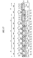
- FIG. 17 is a sectional view of the solid-state image sensor according to the first embodiment of the present invention, in the steps of the method for fabricating the solid-state image sensor, which illustrates the method (Part 15).
- FIG. 18 is a sectional view of the solid-state image sensor according to the first embodiment of the present invention, in the steps of the method for fabricating the solid-state image sensor, which illustrates the method (Part 16).
- FIG. 19 is a sectional view of the solid-state image sensor according to the first embodiment of the present invention, in the steps of the method for fabricating the solid-state image sensor, which illustrates the method (Part 17).
- FIG. 20 is a sectional view of the solid-state image sensor according to the first embodiment of the present invention, in the steps of the method for fabricating the solid-state image sensor, which illustrates the method (Part 18).
- FIG. 21 is a sectional view of the solid-state image sensor according to a modification of the first embodiment of the present invention.
- FIG. 22 is a sectional view of the solid-state image sensor according to a second embodiment of the present invention.
- FIG. 23 is a sectional view of the solid-state image sensor according to the second embodiment of the present invention, in the steps of the method for fabricating the solid-state image sensor, which illustrates the method (Part 1).
- FIG. 24 is a sectional view of the solid-state image sensor according to the second embodiment of the present invention, in the steps of the method for fabricating the solid-state image sensor, which illustrates the method (Part 2).
- FIG. 25 is a sectional view of the solid-state image sensor according to the second embodiment of the present invention, in the steps of the method for fabricating the solid-state image sensor, which illustrates the method (Part 3).
- FIG. 26 is a sectional view of the solid-state image sensor according to the second embodiment of the present invention, in the steps of the method for fabricating the solid-state image sensor, which illustrates the method (Part 4).
- FIG. 27 is a sectional view of the solid-state image sensor according to a modification of the second embodiment of the present invention.
- FIG. 28 is a sectional view of the solid-state image sensor according to a third embodiment of the present invention.
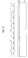
- FIG. 29 is a sectional view of the solid-state image sensor according to the third embodiment of the present invention, in the steps of the method for fabricating the solid-state image sensor, which illustrates the method (Part 1).
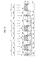
- FIG. 30 is a sectional view of the solid-state image sensor according to the third embodiment of the present invention, in the steps of the method for fabricating the solid-state image sensor, which illustrates the method (Part 2).
- FIG. 31 is a sectional view of the solid-state image sensor according to the third embodiment of the present invention, in the steps of the method for fabricating the solid-state image sensor, which illustrates the method (Part 3).
- FIG. 32 is a sectional view of the solid-state image sensor according to the third embodiment of the present invention, in the steps of the method for fabricating the solid-state image sensor, which illustrates the method (Part 4).
- FIG. 34 is a sectional view of the solid-state image sensor according to the third embodiment of the present invention, in the steps of the method for fabricating the solid-state image sensor, which illustrates the method (Part 6).
- FIG. 35 is a sectional view of the solid-state image sensor according to the third embodiment of the present invention, in the steps of the method for fabricating the solid-state image sensor, which illustrates the method (Part 7).
- FIG. 36 is a sectional view of the solid-state image sensor according to the third embodiment of the present invention, in the steps of the method for fabricating the solid-state image sensor, which illustrates the method (Part 8).
- FIG. 37 is a sectional view of the solid-state image sensor according to a modification of the third embodiment of the present invention.
- the pixels of the black pixel array part 12 are shielded from light with the shield film 58 .
- the pixels of the black pixel array part may be shielded from light with an interconnection layer formed solidly.
- the analog circuit 14 is for processing analog signals, etc. outputted from the pixel part.
- the analog circuit part 14 comprises, e.g., an amplification circuit for amplifies detected light signals, a signal read/noise cancellation circuit for reading signals or canceling noises, an A/D converter for converting analog signals to digital signals, etc.
- noises are cancelled by, e.g., CDS (Correlated Double Sampling).
- the digital circuit part 16 is for digitizing signals, etc. outputted from the analog circuit part 14 and other processing.
- a processor unit for making prescribed signal processing, a timing generator for deciding a timing of reading signals, an SRAM circuit for memorizing data, etc. are formed.
- the I/O circuit part 18 is for inputting/outputting signals to/from the outside.
- the pixel array part 10 is illustrated on the right side of the drawing.
- the black pixel array part 12 is illustrated on the left side of the pixel array part 10 .
- the analog circuit part 14 is illustrated on the left side of the black pixel array part 12 .
- the digital circuit 16 is illustrated on the left side of the analog circuit 14 .
- the I/O circuit part 18 is illustrated on the left side of the digital circuit 16 .
- the region 10 D of the pixel array part 10 on the right side of the drawing is a region where a photodiode (photoelectric conversion device) PD 1 is formed, and the region 10 N of the pixel array part 10 on the left side of the drawing is a region where an NMOS transistor is formed.
- the region 12 D of the black pixel array part 12 on the right side of the drawing is a region where a photodiode PD 2 is formed, and the region 12 N of the black pixel array part 12 on the left side of the drawing is a region where an NOMS transistor is formed.
- the region 14 P of the analog circuit part 14 on the right side of the drawing is a region where a PMOS transistor is formed, and the region 14 N of the analog circuit part 14 on the left side of the drawing is a region where an NMOS transistor is formed.
- the region 16 P of the digital circuit part 16 on the right side of the drawing is a region where a PMOS transistor is formed, and the region 16 N of the digital circuit part 16 on the left side of the drawing is a region where an NMOS transistor is formed.
- the region 18 P of the I/O circuit part 18 on the right side of the drawing is a region where a PMOS transistor is formed, and the region 18 N of the I/O circuit part 18 on the left side of the drawing is a region where an NMOS transistor is formed.
- Device isolation regions 22 for defining the device regions are formed on the surface of a P type semiconductor substrate 20 .
- an N type impurity diffused region 24 a is formed in the semiconductor substrate 20 .
- the N type impurity diffused region 24 a forms the photodiode PD 1 .
- a P type impurity diffused layer 26 is formed on the surface of the device region where the N type impurity diffused region 24 a is formed. Silicon oxide films 30 a , 34 are formed on the P type impurity diffused layer 26 .
- a P type well 28 a is formed in the region 10 N of the pixel array part 10 , where the NMOS transistor is formed.
- a gate electrode 32 is formed on the P type well 28 a with the gate insulation film 30 a formed therebetween.
- the N type lightly doped diffused layer is formed in the semiconductor substrate 20 on both sides of the gate electrode 32 .
- a sidewall insulation film 34 is formed on the side wall of the gate electrode 32 .
- the N type heavily doped diffused layer is formed in the semiconductor substrate 20 on both side of the gate electrode 32 with the sidewall insulation film 34 formed on.
- the N type lightly doped diffused layer and the N type heavily doped diffused layer form a source/drain diffused layer 36 n of the LDD structure.
- the NMOS transistor 38 a including the gate electrode 32 and the source/drain diffused layer 36 n is formed.
- the NMOS transistor 38 a forms a part of the read circuit of, e.g., the pixel array part 10 .
- an N type buried diffused layer 40 a is formed in the semiconductor substrate 20 of the black pixel array part 12 .
- An N type well 42 a is formed, surrounding the region between the surface of the semiconductor substrate 20 and the N type buried diffused layer 40 a .
- the N type well 42 a and the N type buried diffused layer 40 a are connected to each other at the sides of the N type buried diffused layer 40 a .
- a P type well 28 b is formed in the region surrounded by the buried diffused layer 40 a and the N type well 42 a .
- the P type well 28 b is formed in the region 12 N, where the NMOS transistor is formed and also in the region 12 D, where the photodiode is formed.
- the P type well 28 b is isolated from the pixel array part 10 by the N type buried diffused layer 40 a and the N type well 42 a . This structure is called a triple well structure.
- an N type impurity diffused region 24 b is formed in the P type well 28 b .
- the P type impurity diffused layer 26 is formed on the surface of the device region where an N type impurity diffused region 24 b is formed.
- the silicon oxide films 30 a , 34 are formed on the P type impurity diffused layer 26 .
- a gate electrode 32 is formed on the P type well 28 b with the gate insulation film 30 a formed therebetween.
- the N type lightly doped diffused layer is formed in the semiconductor substrate 20 on both side of the gate electrode 32 .
- the sidewall insulation film 34 is formed on the side wall of the gate electrode 32 .
- the N type heavily doped diffused layer is formed in the semiconductor substrate 20 on both sides of the gate electrode 32 with the sidewall insulation film 34 formed on.
- the N type lightly doped diffused layer and the N type heavily doped diffused layer form the source/drain diffused layer 36 n of the LDD structure.
- the NMOS transistor 38 b including the gate electrode and the source/drain diffused layer 36 n is formed.
- the NMOS transistor 38 b forms a part of the read circuit of, e.g., the black pixel array part 12 .
- the N type buried diffused layer 40 b is buried in the semiconductor substrate 20 .
- An N type well 42 b is formed, surrounding the region between the surface of the semiconductor substrate 20 and the buried diffused layer 40 b .
- the N type well 42 b is formed in the device region 14 N, where the NMOS transistor is formed and also in the region 14 P, where the PMOS transistor is formed.
- the N type well 42 b and the buried diffused layer 40 b are connected to each other at the sides of the buried diffused layer 40 b .
- a P type well 44 a is formed in the region surrounded by the buried diffused layer 40 b and the N type well 42 b .
- the P type well 44 a is electrically isolated from the pixel array part 10 by the buried diffused layer 40 b and the N type well 42 b.
- a gate electrode 32 is formed on the P type well 44 a with the gate insulation film 30 b .
- the N type lightly doped diffused layer is formed in the semiconductor substrate 20 on both sides of the gate electrode 32 .
- the sidewall insulation film 34 is formed on the side wall of the gate electrode 32 .
- the N type heavily doped diffused layer is formed in the semiconductor substrate 20 on both sides of the gate electrode 32 with the sidewall insulation film 34 formed on.
- the N type lightly doped diffused layer and the N type heavily doped diffused layer form the source/drain diffused layer 36 n of the LDD structure.
- the NMOS transistor 38 c including the gate electrode 32 and the source/drain diffused layer 36 n is formed.
- a gate electrode 32 is formed with the gate insulation film 30 b formed therebetween.
- the P type lightly doped diffused layer is formed in the semiconductor substrate 20 on both sides of the gate electrode 32 .
- the sidewall insulation film 34 is formed on the side wall of the gate electrode 32 .
- the P type heavily doped diffused layer is formed in the semiconductor substrate 20 on both sides of the gate electrode 32 with the sidewall insulation film 34 formed on.
- the P type lightly doped diffused layer and the P type heavily doped diffused layer form the source/drain diffused layer 36 p of the LDD structure.
- the PMOS transistor 38 d including the gate electrode 32 and the source/drain diffused layer 36 p is formed.
- the NMOS transistor 38 c and the PMOS transistor 38 d form the CMOS circuit.
- the N type buried diffused layer 40 c is buried in the semiconductor substrate 20 .
- An N type well 42 c is formed, surrounding the region between the surface of the semiconductor substrate 20 and the buried diffused layer 40 c .
- the N type well 42 c is formed in the device region 16 N, where the NMOS transistor is formed and also in the region 16 P, where the PMOS transistor is formed.
- the buried diffused layer 40 c and the N type well 42 c are connected to each other at the side of the buried diffused layer 40 c .
- a P type well 44 b is formed in the region surrounded by the buried diffused layer 40 c and the N type well 42 c .
- the P type well 44 b is electrically isolated from the pixel array part 10 by the buried diffused layer 40 c and the N type well 42 c.
- a gate electrode 32 is formed on the P type well 44 b with the gate insulation film 30 b formed therebetween.
- the N type lightly doped diffused layer is formed in the semiconductor substrate 20 on both sides of the gate electrode 32 .
- the sidewall insulation film 34 is formed on the side wall of the gate electrode 32 .
- the N type heavily doped diffused layer is formed in the semiconductor substrate 20 on both sides of the electrode 32 with the sidewall insulation film 34 formed on.
- the N type lightly doped diffused layer and the N type heavily doped diffused layer form the source/drain diffused layer 36 n of the LDD structure.
- the NMOS transistor including the gate electrode 32 and the source/drain diffused layer 36 n is formed.
- a gate electrode 32 is formed on the N type well 42 c with the gate insulation film 30 b formed therebetween.
- the P type lightly doped diffused layer is formed in the semiconductor substrate 20 on both sides of the gate electrode 32 .
- the sidewall insulation film 34 is formed on the side wall of the gate electrode 32 .
- the P type heavily doped diffused layer is formed in the semiconductor substrate 20 on both sides of the gate electrode 32 with the sidewall insulation film 34 formed on.
- the P type lightly doped diffused layer and the P type heavily doped diffused layer form the source/drain diffused layer 36 p of the LDD structure.
- the PMOS transistor 38 f including the gate electrode 32 and the source/drain diffused layer 36 p is formed.
- the NMOS transistor 38 c and the PMOS transistor 38 f form the CMOS circuit.
- the N type buried diffused layer 40 d is buried in the semiconductor substrate 20 .
- An N type well 42 d is formed, surround the region between the surface of the semiconductor substrate 20 and the buried diffused layer 40 d .
- the N type well 42 d is formed in the region 18 N, where the NMOS transistor is formed and also in the region 18 P, where the PMOS transistor is formed.
- the N type well 42 d and the N type buried diffused layer 40 d are connected to each other on the side of the buried diffused layer 40 d .
- a P type well 44 c is formed in the region surrounded by the N type buried layer 40 d and the N type well 42 d .
- the P type well 44 c is electrically isolated from the pixel array part 10 by the buried diffused layer 40 d and the N type well 42 d.
- a gate electrode 32 is formed on the P type well 44 c with the gate insulation film 30 a formed therebetween.
- the N type lightly diffused layer is formed in the semiconductor substrate 20 on both sides of the gate electrode 32 .
- the sidewall insulation film 34 is formed on the sidewall of the gate electrode 32 .
- the N type heavily doped diffused layer is formed in the semiconductor substrate 20 on both sides of the gate electrode 32 with the sidewall insulation film 34 formed on.
- the N type lightly doped diffused layer and the N type heavily doped diffused layer form the source/drain diffused layer 36 n of the LDD structure.
- the NMOS transistor 38 g including the gate electrode 32 and he source/drain diffused layer 36 n is formed.
- a gate electrode 32 is formed on the N type well 42 d with the gate insulation film 30 a formed therebetween.
- the sidewall insulation film 34 is formed on the side wall of the gate electrode 32 .
- the P type source/drain diffused layer 36 p is formed in the semiconductor substrate 20 on both sides of the gate electrode 32 with the sidewall insulation film 34 formed on.
- the PMOS transistor 38 h including the gate electrode 32 and the source/drain diffused layer 36 p is formed.
- the NMOS transistor 38 g and the PMOS transistor 38 h form the CMOS circuit.
- source/drain electrodes 46 a of metal silicide are formed on the source/drain diffused layer 36 n , 36 p . Also on the upper surfaces of the gate electrodes 32 , a metal silicide film 46 b is formed.
- An inter-layer insulation film 48 is formed on the semiconductor substrate 20 with the photodiodes PD 1 , PD 2 , the NMOS transistors 38 a – 38 c , 38 e , 38 g , the PMOS transistors 38 d , 38 f , 38 h , etc. formed on.
- contact holes 50 a and contact holes 50 b are formed respectively down to the source/drain electrodes 46 a and down to the gate electrodes 32 .
- Conductor plugs 52 are buried in the contact holes 50 a , 50 b.
- interconnections 54 are formed, connected to the conductor plugs 52 .
- inter-layer insulation film 48 with the interconnections 54 formed on On the inter-layer insulation film 48 with the interconnections 54 formed on, other interconnection layers and other inter-layer insulation layers 56 are formed respectively in plural layers.
- a shield film 58 is formed on the inter-layer insulation film 56 .
- an opening 60 is formed in for opening the region 10 D of the pixel array part 10 , where the photodiode is formed.
- the photodiode PD 2 of the black pixel array part 12 is shielded from light by the shield film 58 .
- the so-called triple well structure is used in the black pixel array part 12 , the analog circuit part 14 , the digital circuit part 16 and the I/O circuit 18 . That is, in the present embodiment, the P type well 28 b of the black pixel array part 12 is electrically isolated from the pixel array part 10 by the N type well 42 a and the N type buried diffused layer 40 a , the P type well 44 a of the analog circuit 14 is electrically isolated from the pixel array part 10 by the N type well 42 b and the N type buried diffused layer 40 b , the P type well 44 b of the digital circuit 16 is electrically isolated from the pixel array part 10 by the N type well 42 c and the N type buried diffused layer 40 c , and the P type well 44 c of the I/O circuit part 18 is electrically isolated from the pixel array part 10 by the N type well 42 d and the N type well 40 d.
- the P type well 28 b of the black pixel array part 12 is electrically isolated from the pixel array part 10 by the N type well 42 a and the N type buried diffused layer 40 a , so that when relatively intense light is incident on the pixel array part 10 , the inflow of charges into the black pixel array 12 is prevented to thereby obtain stable reference signals.
- the P type well 44 a of the analog circuit part 14 is electrically isolated from the pixel array part 10 by the N type well 42 b and the N type buried diffused layer 40 b , so that the intrusion of noises into the analog circuit part 14 is prevented, and also the noises generated in the analog circuit part 14 are prevented from affecting the other components.
- the P type well 44 b of the digital circuit part 16 is electrically isolated from the pixel array part 10 by the N type well 42 c and the N type buried diffused layer 40 c , so that the intrusion of noises into the digital circuit part 16 is prevented, and also the noises generated in the digital circuit part 16 are prevented from affecting the other components.
- the P type well 44 c of the I/O circuit 18 is electrically isolated from the pixel array part 10 by the N type well 42 d and the N type buried diffused layer 40 d , so that the intrusion of noises into the I/O circuit part 18 is prevented, and also the noises intruding into the I/O circuit part 18 from the outside and the noises generated in the I/O circuit part 18 are prevented from affecting the other components.
- the so-called triple structure is not used in the pixel array part 10 for the following reason.
- the depletion layer is extended to sufficiently deep region of the semiconductor substrate 20 . If the N type impurity diffused region 24 a forming the photodiode PD 1 is formed in the P type well, because of the higher impurity concentration of the P type well than that of the semiconductor substrate 20 , the depletion layer cannot easily extend when light is incident on the photodiode PD 1 .
- the impurity concentration of the P type well is set lower so as to make it easy for the depletion layer to extend, depletion layer is hindered from extending by the N type buried diffused layer formed below the P type well. Accordingly, the use of the triple well structure in the pixel array part 10 makes it very difficult to realize high quality image.
- the triple structure is not used in the pixel array part 10 but used in the black pixel array part 12 , the analog circuit part 14 , the digital circuit part 16 and the I/O circuit 18 , whereby the pixel array part 10 is kept from being affected by the noises.
- the solid-state image sensor according to the present embodiment is characterized mainly in that the triple well structure is not used in the pixel array part 10 but is used in the black pixel array part 12 , the analog circuit part 14 , the digital circuit part 16 and the I/O circuit part 18 .
- the triple structure is used in the black pixel part 12 , the analog circuit part 14 , the digital circuit part 16 and the I/O circuit part 18 , whereby the pixel array part 10 is kept form being affected by noises. Furthermore, the pixel array part 10 , which does not use the triple well structure, can perform highly efficient photoelectric conversion. Accordingly, the solid-state image sensor according to the present embodiment can realize high quality image quality.
- Patent Reference 1 discloses a technique of stabilize the black level by preventing the inflow of charges into the black pixel array part when intense light is incident on the pixels of the pixel array parts. However, it is difficult to realize the drastic improvement of the image quality only by stabilizing the black level. Patent Reference 1 neither discloses nor suggests the technique of the present invention that the triple well structure is used in the analog circuit part, the digital circuit part and the input/output circuit part to thereby realize the drastic improvement of the image quality.
- FIGS. 3 to 20 are sectional views of the solid-state image sensor according to the present embodiment in the steps of the method for fabricating the solid-state image sensor, which illustrate the method.
- the P type semiconductor substrate 20 is prepared.
- the semiconductor substrate 20 is, e.g., an epitaxial substrate with, e.g., a 11 ⁇ m-thickness silicon layer epitaxially grown on a silicon substrate.
- the resistivity of the semiconductor substrate 10 is, e.g., 10 ⁇ cm.
- trenches 62 of an about 250 nm-depth are formed in the semiconductor substrate 20 .
- a silicon oxide film is formed on the entire surface.
- the silicon oxide film is polished by, e.g., CMP until the surface of the semiconductor substrate 20 is exposed.
- the silicon oxide film is thus buried in the trenches 62 to form the device isolation regions 22 .
- the device isolation regions 22 are formed by STI (Shallow Trench Isolation).
- a photoresist film 64 is formed on the entire surface by spin coating.
- the photoresist film 64 is patterned by photolithography.
- an opening 66 a is formed to expose the black pixel array part 12
- an opening 66 b is formed to expose the region 14 N of the analog circuit part 14 , where the NMOS transistor is to be formed
- an opening 66 c is formed to expose the region 16 N of the digital circuit part 16 , where the NMOS transistor is to be formed
- an opening 66 d is formed to expose the region 18 N of the I/O circuit part 18 , where the NMOS transistor is to be formed.
- an N type dopant impurity is implanted by ion implantation.
- the N type dopant impurity is, e.g., phosphorus (P + ).
- Conditions for the ion implantations are, e.g., a 1 MeV acceleration energy and a 1 ⁇ 10 13 –5 ⁇ 10 13 cm ⁇ 2 .
- the N type buried diffused layer 40 a – 40 d is buried.
- the buried diffused layer 40 a – 40 d is buried in the region which is about 1–1.5 ⁇ m deep from the surface of the semiconductor substrate 20 . Then, the photoresist film 64 is released.
- a photoresist film 68 is formed on the entire surface by spin coating.
- the photoresist film 68 is patterned by photolithography.
- an opening 70 a for exposing the region 14 N of the analog circuit part 14 , where the NMOS transistor is to be formed, an opening 70 b for exposing the region 16 N of the digital circuit part 16 , where the NMOS transistor is to be formed, and an opening 70 c for exposing the region 18 N of the I/O circuit part 18 , where the NMOS transistor is to be formed are formed in the photoresist film 68 .
- a P type dopant impurity is introduced by ion implantation.
- the P type dopant impurity is, e.g., boron (B + ).
- Conditions for the ion implantation are, e.g., a 300–500 keV and a 1 ⁇ 10 13 –5 ⁇ 10 13 cm ⁇ 2 .
- the P type wells 44 a – 44 c are formed.
- a threshold voltage control layer for controlling threshold voltages of the NMOS transistors 38 c , 38 e , 38 g (see FIG. 2 ) may be formed by implanting a dopant impurity in the semiconductor substrate 20 with the photoresist film 58 as a mask, before the photoresist film 68 is released.
- a P type dopant impurity is introduced in a relative shallow region of the semiconductor substrate 20 by ion implantation with the photoresist film 68 as the mask.
- the P type dopant impurity is, e.g., boron.
- Conditions for the ion implantation are, e.g., an acceleration energy of 50 keV or below, and a 1 ⁇ 10 12 –7 ⁇ 10 12 cm ⁇ 2 dose. Then, the photoresist film 68 is released.
- a photoresist film 72 is formed on the entire surface by spin coating.
- the photoresist film 72 is patterned by photolithography.
- openings 74 a – 74 d for exposing the peripheral edges of the region where the buried diffused layers 40 a – 40 d are formed.
- the opening 74 b for exposing the peripheral edge of the region where the buried diffused layer 40 b is formed is formed, exposing also the peripheral edge of the region 14 P of the analog circuit part 14 , where the PMOS transistor is to be formed.
- the opening 74 c for exposing the peripheral edge of the region where the buried diffused layer 40 c is formed is formed, exposing also the region 16 P of the digital circuit part 16 , where the PMOS transistor is to be formed.
- the opening 74 d for exposing the peripheral edge of the region where the buried diffused layer 40 d is formed is formed, exposing also the region 18 P of the I/O circuit 18 , where the PMOS transistor is to be formed.
- an N type dopant impurity is introduced by ion implantation with the photoresist film 72 as the mask.
- the N type dopant impurity is, e.g., phosphorus (P + ).
- Conditions for the ion implantation are, e.g., a 500–700 keV acceleration energy and a 1 ⁇ 10 13 –5 ⁇ 10 13 cm ⁇ 2 .
- the N type wells 42 a – 42 d are formed in the black pixel array part 12 , the analog circuit part 14 , the digital circuit part 16 and the I/O circuit 18 .
- the N type wells 42 a – 42 d and the N type buried diffused layers 40 a – 40 d are connected each other at the sides of the N type buried diffused layer 40 a – 40 d.
- a threshold voltage control layer for controlling threshold voltages of the PMOS transistors 38 d , 38 f , 38 h (see FIG. 2 ) may be formed by implanting a dopant impurity in the semiconductor substrate 20 with the photoresist film 72 as a mask, before the photoresist film 72 is released.
- an N type dopant impurity is introduced in a relative shallow region of the semiconductor substrate 20 by ion implantation with the photoresist film 72 as the mask.
- the N type dopant impurity is, e.g., arsenic (As + ).
- Conditions for the ion implantation are, e.g., an acceleration energy of 200 keV or below, and a 1 ⁇ 10 12 –5 ⁇ 10 12 cm ⁇ 2 dose. Then, the photoresist film 72 is released.
- a photoresist film 76 is formed on the entire surface by spin coating.
- the photoresist film 76 is patterned by photolithography.
- a P type dopant impurity is introduced by ion implantation with the photoresist film 76 as the mask,
- the P type dopant impurity is, e.g., boron.
- Conditions for the ion implantation are, e.g., a 300–500 keV acceleration energy and a 1 ⁇ 10 13 –5 ⁇ 10 13 cm ⁇ 2 .
- the P type well 28 a is formed in the region 10 N of the pixel array part 10 , where the NMOS transistor is to be formed.
- the P type well 28 b is formed in the region of the black pixel array part 12 , which is surrounded by the N type well 42 a and the buried diffused layer 28 b.
- a threshold voltage control layer for controlling threshold voltages of the NMOS transistors 38 a , 38 b (see FIG. 2 ) may be formed by implanting a dopant impurity in the semiconductor substrate 20 with the photoresist film 76 as a mask, before the photoresist film 76 is released.
- a P type dopant impurity is introduced in a relative shallow region of the semiconductor substrate 20 by ion implantation with the photoresist film 76 as the mask.
- the P type dopant impurity is, e.g., boron.
- Conditions for the ion implantation are, e.g., a 50 keV acceleration energy and a 2 ⁇ 10 12 –7 ⁇ 10 12 cm ⁇ 2 dose. Then, the photoresist film 76 is released.
- a photoresist film 80 is formed on the entire surface by spin coating.
- the photoresist film 80 is patterned by photolithography to form in the photoresist film 80 an opening 82 a for exposing the region of the pixel array part 10 , where the photodiode PD 1 is to be formed, and an opening 82 b of the black pixel array part 12 , where the photodiode PD 2 is to be formed.
- an N type dopant impurity is introduced by ion implantation with the photoresist film 80 as the mask.
- the dopant impurity is, e.g., phosphorus.
- Conditions for the ion implantation are, e.g., a 300–500 keV acceleration energy and a 1 ⁇ 10 12 –5 ⁇ 10 12 cm ⁇ 2 .
- the N type impurity diffused regions 24 a , 24 b forming the photodiode PD 1 , PD 2 are formed.
- the ion implantation may be repeated by plural times to form the N type impurity diffused region 24 a , 24 b .
- conditions for the first ion implantation are, e.g., a 300–500 keV acceleration energy and a 1 ⁇ 10 12 –5 ⁇ 10 12 cm ⁇ 2 dose
- the conditions for the second ion implantation are, e.g., an about 100 keV acceleration energy and a 1 ⁇ 10 12 –5 ⁇ 10 12 cm ⁇ 2 dose.
- the N type impurity diffused regions 24 a , 24 b may be thus formed. Then, the photoresist film 80 is released.
- the gate insulation film 30 of, e.g., a 5–8 nm-thickness is formed on the entire surface.
- a photoresist film 84 is formed on the entire surface by spin coating.
- an opening 86 for exposing the region 14 , where the analog circuit part is to be formed and the region 16 , where the digital circuit part is to be formed is formed in the photoresist film 84 by photolithography.
- the gate insulation film 30 exposed in the opening 86 is etched off.
- the etchant is, e.g., hydrofluoric acid. Then, the photoresist film 84 is released.
- the gate insulation film 30 b is formed on the exposed surface of the semiconductor substrate 20 while adding to the thickness of the gate insulation film 30 .
- the conditions for the thermal oxidation are set so that the thermal oxide film is formed in a 3 nm-thickness on the exposed surface of the semiconductor substrate 20 .
- the gate insulation film 30 b is formed in, e.g., a 3 nm-thickness in the analog circuit part 14 and the digital circuit part 16 .
- the film thickness of the gate insulation film 30 a there is, e.g., about 8–10 nm (see FIG. 11 ).
- a polysilicon film 32 of, e.g., a 150–200 nm-thickness is formed on the entire surface.
- the polysilicon film 32 is patterned by photolithography.
- the gate electrodes 32 of the polysilicon are formed.
- a photoresist film (not illustrated) is formed on the entire surface by spin coating.
- openings for exposing the regions 10 N, 12 N, 14 N, 16 N, 18 N for the NMOS transistors to be formed are formed in the photoresist film.
- an N type dopant impurity is introduced into the semiconductor substrate 20 by ion implantation.
- the dopant impurity is, e.g., arsenic (As + ).
- Conditions for the ion implantation are, e.g., an acceleration energy of 15 keV or below, and a 2 ⁇ 10 14 –7 ⁇ 10 14 cm ⁇ 2 dose.
- the N type lightly doped diffused layer 35 n is formed in the semiconductor substrate 20 on both sides of the gate electrodes 32 . Then, the photoresist film is released.
- a photoresist film (not illustrated) is formed on the entire surface by spin coating.
- openings for exposing the regions 14 P, 16 P, where the PMOS transistors are to be formed, are formed in the photoresist film.
- a P type dopant impurity is introduced into the semiconductor substrate 20 by the ion implantation with the photoresist film and the gate electrodes 32 as the mask.
- the dopant impurity is, e.g., BF 2 + .
- Conditions for the ion implantation are, e.g., an acceleration energy of 15 keV or below, and a 2 ⁇ 14 14 –7 ⁇ 10 14 cm ⁇ 2 dose.
- the P type lightly doped diffused layer 35 p is formed in the semiconductor substrate 20 on both sides of the gate electrodes 32 . Then, the photoresist film is released.
- a photoresist film (not illustrated) is formed on the entire surface by spin coating.
- openings for exposing the regions 10 D, 12 D for the photodiodes to be formed in are formed in the photoresist film.
- a P type dopant impurity is introduced into the semiconductor substrate 20 by ion implantation with the photoresist film as the mask.
- the dopant impurity is, e.g., boron (B + ).
- Conditions for the ion implantation are, e.g., a 15 keV acceleration energy and a 1 ⁇ 10 13 –5 ⁇ 10 13 cm ⁇ 2 dose.
- the P type impurity diffused layer 26 is formed on the surface of the semiconductor substrate 20 in the regions 10 D, 12 D where the photodiodes are to be formed. Then, the photoresist film is released.
- the silicon oxide film 34 of a 100 nm-thickness is formed on the entire surface by, e.g., CVD.
- the silicon oxide film 34 is to be the sidewall insulation film on the side walls of the gate electrodes 32 .
- the silicon oxide film 34 functions also as a protection film for protecting the regions where the metal silicide film 46 a , 46 b is not to be formed.
- a photoresist film 88 is formed on the entire surface by spin coating.
- the photoresist film 88 is patterned by photolithography to cover the regions where the metal silicide film 46 a , 46 b is not to be formed (see FIG. 2 ).
- the silicon oxide film 34 is anisotropically etched.
- the sidewall insulation film of the silicon oxide film 34 is formed on the side walls of the gate electrodes 32 .
- the silicon oxide film 34 remains in the regions where the metal silicide film 46 a , 46 b is not to be formed. Then, the photoresist film 88 is released.
- a photoresist film (not illustrated) is formed on the entire surface by spin coating.
- a photoresist film for exposing the regions 10 N, 12 N, 14 N, 16 N, 18 N, where the NMOS transistors are to be formed is formed.
- an N type dopant impurity is implanted by ion implantation with the photoresist film and the gate electrodes 32 as the mask.
- the dopant impurity is, e.g., phosphorus (P + )
- Conditions for the ion implantation are, e.g., an acceleration energy of 20 keV or below, and a 1 ⁇ 10 15 –5 ⁇ 10 15 cm ⁇ 2 dose.
- the N type heavily doped diffused layer is formed in the semiconductor substrate 20 on both sides of the gate electrodes 32 .
- the N type lightly doped diffused layer 35 n and the N-heavily doped diffused layer form the source/drain diffused layer 36 n of the LDD structure.
- the photoresist film is released.
- a photoresist film (not illustrated) is formed on the entire surface by spin coating.
- openings for exposing the regions 14 P, 16 P, 18 P, where the PMOS transistors are to be formed, are formed in the photoresist film.
- a P type dopant impurity is introduced by ion implantation with the photoresist film and the gate electrodes 32 as the mask.
- the P type dopant impurity is, e.g., boron (B + ).
- Condition for the ion implantation are, e.g., an acceleration energy of 10 keV or below and a 1 ⁇ 10 15 –5 ⁇ 10 15 cm ⁇ 2 dose.
- the P type heavily dopes diffused layer is formed in the semiconductor substrate 20 on both sides of the gate electrodes 32 .
- the P type lightly doped diffused layer 35 p and the P type heavily dopes diffused layer form the source/drain diffused layer 36 p of the LDD structure in the region 14 P of the analog circuit part 14 , where the PMOS transistor is to be formed and in the region 16 P of the digital circuit part 16 , where the PMOS transistor is to be formed.
- the source/drain diffused layer 36 p of the P type heavily doped diffused layer is formed in the region 18 P of the I/O circuit part 18 , where the PMOS transistor is to be formed. Then, the photoresist film is released (see FIG. 17 ).
- a metal film of a 10 nm-thickness cobalt film is formed by, e.g., puttering.
- the metal silicide film 46 a , 46 b of cobalt silicide is formed.
- the atmosphere for the thermal processing is, e.g., nitrogen atmosphere.
- the temperature for the thermal processing is, e.g., 500° C.
- the thermal processing period of time is, e.g., 30 seconds.
- the metal silicide film 46 a which are formed on the surface of the source/drain diffused layer 36 p , 36 n , functions as the source/drain electrodes.
- the metal silicide film 46 b is formed also on the surfaces of the gate electrodes 32 .
- the metal film is cobalt film here but is not limited to cobalt film.
- the metal film may be, e.g., titanium film, and in this case, the metal silicide film is titanium silicide film.
- the silicon oxide film 48 of a 1500 nm-thickness is formed on the entire surface by, e.g., plasma CVD.
- the contact hole 50 a , 50 b are formed by photolithography in the inter-layer insulation film 48 respectively down to the source/drain electrode 46 a and down to the gate electrode 46 b.
- a 300 nm-thickness tungsten film is formed on the entire surface by, e.g., CVD.
- a 500 nm-thickness aluminum film 54 is formed by, e.g., sputtering.
- the aluminum film 54 is patterned by photolithography.
- the interconnections (a first metal interconnection layer) 54 of aluminum are formed.
- the step of forming the inter-layer insulation film 56 , the step of forming contact holes and the step of forming interconnections are sequentially repeated to thereby form a plurality of interconnection layers 56 , the interconnection layers, etc.
- the shield film 58 is formed on the inter-layer insulation film 56 .
- the solid-state image sensor according to the present embodiment is fabricated.
- FIG. 21 is a sectional view of the solid-state image sensor according to the present modification.
- the solid-state image sensor according to the present modification is characterized mainly in that the N type well 42 e of the digital circuit part 16 and the N type well 42 e of the I/O circuit part 18 are formed integral with each other, in other words, the N type well 42 e of the digital circuit part 16 and the N type well 42 e of the I/O circuit part 18 are formed continuous to each other.
- the N type buried diffused layer 40 c and the N type well 42 e are connected to each other at the side of the buried diffused layer 40 c.
- the N type well 42 e of the digital circuit part 16 and the N type well 42 e of the I/O circuit part 16 may be formed continuous to each other.
- FIG. 22 is a sectional view of the solid-state image sensor according to the present embodiment.
- the same members of the present invention as those of the solid-state image sensor according to the first embodiment and the method for fabricating the same illustrated in FIGS. 1 to 21 are represented by the same reference numbers not to repeat or to simplify their explanation.
- the solid-state image sensor according to the present embodiment is characterized mainly in that device isolation regions 22 a are formed by LOCOS (Local oxidation of Silicon).
- LOCOS Local oxidation of Silicon
- the solid-state image sensor can have improved image quality, as does the solid-state image sensor according to the first embodiment.
- FIGS. 23 to 26 are sectional views of the solid-state image sensor according to the present embodiment in the steps of the method for fabricating the solid-state image sensor, which illustrate the method.
- a 3–10 nm-thickness silicon oxide film 90 is formed on the entire surface by, e.g., thermal oxidation.
- a 100–150 nm-thickness silicon nitride film 92 is formed on the entire surface by, e.g., CVD.
- a photoresist film 94 is formed on the entire surface by spin coating.
- openings 96 for exposing the regions for the device isolation regions 22 a to be formed in are formed in the photoresist film 94 by photolithography.
- the photoresist film 94 As the mask, the silicon nitride film 92 and the silicon oxide film 90 are etched. Then, the photoresist film 94 is released.
- the semiconductor substrate 20 is oxidized by thermal oxidation selectively at the parts which are not covered by the silicon nitride film 92 .
- the device isolation regions 22 a of the silicon oxide film are formed by LOCOS.
- the etchant is, e.g., boiled phosphoric acid (see FIG. 25 ).
- the solid-state image sensor according to the present embodiment is fabricated (see FIG. 26 ).
- FIG. 27 is a sectional view of the solid-state image sensor according to the present modification.
- the solid-state image sensor according to the present modification is characterized mainly in that the N type well 42 e of a digital circuit part 16 and the N type well 42 e of an I/O circuit part 18 are formed integral with each other.
- the N type well 42 e of the digital circuit part 16 and the N type well 42 e of the I/O circuit 18 are formed continuous to each other.
- the N type well 42 e of the digital circuit part 16 and the N type well 42 e of the I/O circuit part 18 may be formed integral with each other.
- FIG. 28 is a sectional view of the solid-state image sensor according to the present embodiment.
- the same members of present embodiments as those of the solid-state image sensor according to the first or the second embodiment and the method for fabricating the semiconductor device illustrated in FIGS. 1 to 27 are represented by the same reference numbers not to repeat or to simplify their explanation.
- the solid-state image sensor according to the present embodiment is characterized mainly in that a P type well is formed in an N type well to thereby form the triple structure.
- an N type impurity diffused region 24 c is formed in a semiconductor substrate 20 .
- the N type impurity diffused region 24 c forms a photodiode PD 1 .
- a P type well 100 a is formed in a region 10 N of the pixel array part 10 , where an NMOS transistor is formed.
- An NMOS transistor 38 a is formed o the P type well 100 a.
- An N type well 98 a is formed in the semiconductor substrate 20 of a black pixel array part 12 .
- a P type well 100 b is formed in the N type well 98 a .
- the P type well 100 b is formed by implanting a P type dopant impurity into the N type well 98 a .
- the P type well 100 b is formed in a region 12 N where an NMOS transistor is formed and also in a region 12 D where a photodiode PD 2 is formed.
- the P type well 100 b is electrically isolated from the pixel array part 10 by the N type well 98 a.
- an N type impurity diffused region 24 d is formed in the P type well 100 b.
- an NMOS transistor 38 b is formed on the P type well 100 b.
- an N type well 98 b is formed in the semiconductor substrate 20 of an analog circuit part 14 .
- the N type well 98 b is formed in a region 14 N where an NMOS transistor is formed and also in a region 14 P where a PMOS transistor is formed.
- a P type well 100 c is formed in the N type well 98 b .
- the P type well 100 c is formed by implanting a P type dopant impurity into the N type well 98 b .
- the P type well 100 c is electrically isolated from the pixel array part 10 by the N type well 98 b .
- An NMOS transistor 38 c is formed on the P type well 100 c .
- a PMOS transistor 38 d is formed on the N type well 98 b.
- an N type well 98 c is formed in the semiconductor substrate 20 of a digital circuit part 16 .
- the N type well 98 c is formed in a region 16 N where an NMOS transistor is formed and also in a region 16 P where a PMOS transistor is formed.
- a P type well 100 d is formed in the N type well 98 c .
- the P type well 100 d is formed by implanting a P type dopant impurity into the N type well 98 c .
- the P type well 100 d is electrically isolated from the pixel array part 10 by the N type well 98 c .
- An NMOS transistor 38 e is formed on the P type well 100 d .
- a PMOS transistor 38 f is formed on the N type well 98 c.
- an N type well 98 d is formed in the semiconductor substrate 20 of an I/O circuit part 18 .
- the N type well 98 d is formed in a region 18 N where an NMOS transistor is formed and also in a region 18 P where a PMOS transistor is formed.
- a P type well 100 e is formed in the N type well 98 d .
- the P type well 100 e is formed by implanting a P type dopant impurity into the N type well 98 d .
- the P type well 100 e is electrically isolated from the pixel array part 10 by the N type well 98 d .
- An NMOS transistor 38 g is formed on the P type well 100 e .
- a PMOS transistor 38 h is formed on the N type well 98 d.
- the solid-state image sensor according to the present embodiment is formed.
- the P type well 100 b – 100 e are formed by implanting P type dopant impurity into the N type well 98 a – 98 d.
- FIGS. 29 to 36 are sectional views of the solid-state image sensor according to the present embodiment in the steps of the method for fabricating the solid-state image sensor, which illustrate the method.
- a 3–10 nm-thickness silicon oxide film 90 is formed on the entire surface by, e.g., thermal oxidation.
- a 100–150 nm-thickness silicon nitride film 92 is formed on the entire surface by, e.g., CVD.
- a photoresist film 94 is formed on the entire surface by spin coating.
- openings 96 for exposing the regions where device isolation regions 22 a are to be formed are formed in the photoresist film 94 by photolithography.
- the photoresist film 94 as the mask, the silicon nitride film 92 and the silicon oxide film 90 are etched. Then, the photoresist film 94 is released.
- a photoresist film 102 is formed on the entire surface by pin coating.
- an opening 104 a for exposing the region 12 , where the black array pixel array part is to be formed, an opening 104 b for exposing the region 14 , where the analog circuit part is to be formed, an opening 104 c for exposing the region 16 , where the digital circuit part is to be formed, and an opening 104 d for exposing the region 18 , where the I/O circuit part is to be formed are formed in the photoresist film 102 by photolithography.
- an N type dopant impurity is introduced into the semiconductor substrate 20 by ion implantation with the photoresist film 102 as the mask.
- Conditions for the ion implantation are, e.g., a 150–300 keV acceleration energy and a 1 ⁇ 10 13 –5 ⁇ 10 13 cm ⁇ 2 dose.
- the N type wells 98 a – 98 d are formed in the semiconductor substrate.
- the photoresist film 102 is released.
- thermal processing is performed to diffuse the dopant impurity in the N type wells 98 a – 98 d .
- the atmosphere for the thermal processing is, e.g., nitrogen atmosphere.
- the thermal processing temperature is, e.g., 1100° C.
- the thermal processing period of time is, e.g., 100 minutes.
- the semiconductor substrate 20 is oxidized by thermal oxidation selectively at the parts thereof which are not covered by the silicon nitride film 92 .
- the device isolation regions 22 a of the silicon oxide film are formed.
- the device isolation regions 22 a are formed by LOCOS (see FIG. 32 ).
- the N type wells 98 a – 98 d are formed down to, e.g., an bout 3 ⁇ m-depth from the surface of the semiconductor substrate 20 .
- the silicon nitride film 92 is etched off.
- the etchant is, e.g., boiled phosphoric acid.
- the device isolation regions 22 a are formed here after the thermal processing for diffusing the N type dopant impurity implanted in the N type wells 98 a – 98 d has been performed, but the thermal processing for diffusing the N type dopant impurity may be performed after the device isolation regions 22 a have been formed.
- the photoresist film 106 is patterned by photolithography.
- a P type dopant impurity is introduced into the semiconductor substrate 20 by ion implantation with the photoresist film 106 as the mask.
- the P type dopant impurity is, e.g., boron.
- Conditions for the ion implantation are, e.g., a 100–300 keV acceleration energy and a 1 ⁇ 10 13 –5 ⁇ 10 13 cm ⁇ 2 dose.
- a relatively thick gate insulation film 30 a is formed in the pixel array part 10 , the black pixel array part 12 and the I/O circuit part 18 , and the relatively thin gate insulation film 30 b is formed in the digital circuit part 14 and the analog circuit part 16 (see FIG. 34 ).
- a threshold voltage control layer for controlling threshold voltages of the transistors 38 may be formed by implanting a dopant impurity into the entire surface of the semiconductor substrate 20 before or immediately after the step of forming the gate insulation film 30 a , 30 b .
- the dopant impurity is, e.g., boron.
- Conditions for the ion implantation are, e.g., a 50 keV acceleration energy or below, and a 1 ⁇ 10 12 –7 ⁇ 10 12 cm ⁇ 2 dose.
- the gate electrodes 32 is formed.
- a photoresist film 110 is formed on the entire surface by spin coating.
- the photoresist film 110 is patterned by photolithography.
- an opening 112 a for exposing the region 10 D of the pixel array part 10 , where the photodiode is to be formed and an opening 112 b for exposing the region 12 D of the black pixel array part 12 , where the photodiode is to be formed.
- an N type dopant impurity is introduced by ion implantation with the photoresist film 110 as the mask.
- the dopant impurity is, e.g., phosphorus.
- Conditions for the ion implantation are, e.g., a 20–500 keV acceleration energy and a 1 ⁇ 10 14 –5 ⁇ 10 15 cm ⁇ 2 dose.
- the N type impurity diffused regions 24 c , 24 d forming the photodiodes PD 1 , PD 2 are formed.
- the photoresist film 110 is released.
- the solid-state image sensor according to the present embodiment is fabricated (see FIG. 36 ).
- FIG. 37 is a sectional view of the solid-state image sensor according to the present modification.
- the solid-state image sensor according to the present modification is characterized mainly in that the N type well 98 e of the digital circuit part 16 and the N type well 98 e of the I/O circuit part 18 are formed integral with each other. In other words, the N type well 98 e of the digital circuit part 16 and the N type well 98 e of the I/O circuit part 18 are formed continuous to each other.
- the N type well 98 e of the digital circuit part 16 and the N type well 98 e of the I/O circuit part 18 may be formed integral with each other.
- the semiconductor substrate 20 is a P type semiconductor substrate.
- the semiconductor substrate 20 may be an N type semiconductor substrate, and in this case, the conduction types of the respective components are set oppositely.
Landscapes
- Solid State Image Pick-Up Elements (AREA)
- Transforming Light Signals Into Electric Signals (AREA)
Applications Claiming Priority (2)
| Application Number | Priority Date | Filing Date | Title |
|---|---|---|---|
| JP2004-210081 | 2004-07-16 | ||
| JP2004210081A JP2006032688A (ja) | 2004-07-16 | 2004-07-16 | 固体撮像装置 |
Publications (2)
| Publication Number | Publication Date |
|---|---|
| US20060011956A1 US20060011956A1 (en) | 2006-01-19 |
| US7005690B2 true US7005690B2 (en) | 2006-02-28 |
Family
ID=34930903
Family Applications (1)
| Application Number | Title | Priority Date | Filing Date |
|---|---|---|---|
| US11/003,380 Expired - Lifetime US7005690B2 (en) | 2004-07-16 | 2004-12-06 | Solid-state image sensor |
Country Status (6)
| Country | Link |
|---|---|
| US (1) | US7005690B2 (de) |
| EP (1) | EP1617480B1 (de) |
| JP (1) | JP2006032688A (de) |
| KR (1) | KR100671807B1 (de) |
| CN (1) | CN100418230C (de) |
| TW (1) | TWI249850B (de) |
Cited By (4)
| Publication number | Priority date | Publication date | Assignee | Title |
|---|---|---|---|---|
| US20060202295A1 (en) * | 2005-03-11 | 2006-09-14 | Tien-Chi Wu | Method and structure for reducing noise in CMOS image sensors |
| US20070041062A1 (en) * | 2005-08-22 | 2007-02-22 | Micron Technology, Inc. | Method and apparatus for shielding correction pixels from spurious charges in an imager |
| US20070284679A1 (en) * | 2006-06-06 | 2007-12-13 | Emi Ohtsuka | MOS solid-state image pickup device and manufacturing method thereof |
| US20110164161A1 (en) * | 2008-06-11 | 2011-07-07 | Crosstek Capital, LLC | Method of manufacturing cmos image sensor using double hard mask layer |
Families Citing this family (14)
| Publication number | Priority date | Publication date | Assignee | Title |
|---|---|---|---|---|
| JP4584159B2 (ja) * | 2006-02-24 | 2010-11-17 | セイコーインスツル株式会社 | 半導体装置及び半導体装置の製造方法 |
| US20070246788A1 (en) * | 2006-04-21 | 2007-10-25 | Mauritzson Richard A | N-well barrier pixels for improved protection of dark reference columns and rows from blooming and crosstalk |
| JP2007317741A (ja) * | 2006-05-23 | 2007-12-06 | Matsushita Electric Ind Co Ltd | 固体撮像装置およびその製造方法 |
| JP4793402B2 (ja) | 2008-04-21 | 2011-10-12 | ソニー株式会社 | 固体撮像装置とその製造方法、及び電子機器 |
| KR101435519B1 (ko) * | 2008-07-24 | 2014-08-29 | 삼성전자주식회사 | 광 포커싱 구조를 가진 이미지 센서 |
| CN101388393B (zh) * | 2008-08-26 | 2012-11-14 | 矽创电子股份有限公司 | 点转换系统的极性切换结构 |
| US8253200B2 (en) | 2008-11-19 | 2012-08-28 | Omnivision Technologies, Inc. | Lightly-doped drains (LDD) of image sensor transistors using selective epitaxy |
| JP5810493B2 (ja) * | 2010-09-03 | 2015-11-11 | ソニー株式会社 | 半導体集積回路、電子機器、固体撮像装置、撮像装置 |
| US9153565B2 (en) | 2012-06-01 | 2015-10-06 | Taiwan Semiconductor Manufacturing Company, Ltd. | Image sensors with a high fill-factor |
| US8629524B2 (en) | 2012-04-27 | 2014-01-14 | Taiwan Semiconductor Manufacturing Company, Ltd. | Apparatus for vertically integrated backside illuminated image sensors |
| US10090349B2 (en) | 2012-08-09 | 2018-10-02 | Taiwan Semiconductor Manufacturing Company, Ltd. | CMOS image sensor chips with stacked scheme and methods for forming the same |
| US9537040B2 (en) * | 2013-05-09 | 2017-01-03 | United Microelectronics Corp. | Complementary metal-oxide-semiconductor image sensor and manufacturing method thereof |
| JP6484513B2 (ja) * | 2014-10-08 | 2019-03-13 | 株式会社テクノロジーハブ | 画像センサ |
| WO2023189964A1 (ja) * | 2022-03-31 | 2023-10-05 | ラピスセミコンダクタ株式会社 | 半導体装置、および半導体装置の製造方法 |
Citations (7)
| Publication number | Priority date | Publication date | Assignee | Title |
|---|---|---|---|---|
| JPH05115047A (ja) | 1991-10-22 | 1993-05-07 | Olympus Optical Co Ltd | 固体撮像素子 |
| JPH05129572A (ja) | 1991-10-31 | 1993-05-25 | Canon Inc | 固体撮像装置 |
| GB2335097A (en) | 1998-03-04 | 1999-09-08 | Fujitsu Ltd | Digital to analog converter |
| US6169318B1 (en) * | 1998-02-23 | 2001-01-02 | Polaroid Corporation | CMOS imager with improved sensitivity |
| JP2002199289A (ja) | 2000-12-25 | 2002-07-12 | Canon Inc | 光電変換装置およびそれを有する固体撮像システム |
| JP2002329854A (ja) | 2001-04-26 | 2002-11-15 | Fujitsu Ltd | 固体撮像装置 |
| JP2002334974A (ja) | 2001-05-07 | 2002-11-22 | Nikon Corp | 固体撮像装置及びその製造方法 |
Family Cites Families (10)
| Publication number | Priority date | Publication date | Assignee | Title |
|---|---|---|---|---|
| US5324982A (en) * | 1985-09-25 | 1994-06-28 | Hitachi, Ltd. | Semiconductor memory device having bipolar transistor and structure to avoid soft error |
| JPS63102371A (ja) * | 1986-10-20 | 1988-05-07 | Matsushita Electronics Corp | 半導体装置の製造方法 |
| JP3254865B2 (ja) * | 1993-12-17 | 2002-02-12 | ソニー株式会社 | カメラ装置 |
| JP3208307B2 (ja) * | 1995-11-27 | 2001-09-10 | 三洋電機株式会社 | 光半導体装置 |
| JPH09246514A (ja) * | 1996-03-12 | 1997-09-19 | Sharp Corp | 増幅型固体撮像装置 |
| JP3457551B2 (ja) * | 1998-11-09 | 2003-10-20 | 株式会社東芝 | 固体撮像装置 |
| JP2000232214A (ja) * | 1999-02-12 | 2000-08-22 | Nikon Corp | 半導体集積回路および固体撮像素子 |
| JP2003274292A (ja) * | 2002-03-14 | 2003-09-26 | Sony Corp | 固体撮像装置およびその駆動方法 |
| TWI289905B (en) * | 2002-07-23 | 2007-11-11 | Fujitsu Ltd | Image sensor and image sensor module |
| JP3792628B2 (ja) * | 2002-09-02 | 2006-07-05 | 富士通株式会社 | 固体撮像装置及び画像読み出し方法 |
-
2004
- 2004-07-16 JP JP2004210081A patent/JP2006032688A/ja active Pending
- 2004-12-06 US US11/003,380 patent/US7005690B2/en not_active Expired - Lifetime
- 2004-12-07 TW TW093137773A patent/TWI249850B/zh not_active IP Right Cessation
- 2004-12-10 EP EP04257686A patent/EP1617480B1/de not_active Expired - Lifetime
- 2004-12-21 KR KR1020040109650A patent/KR100671807B1/ko not_active Expired - Fee Related
-
2005
- 2005-01-06 CN CNB2005100042556A patent/CN100418230C/zh not_active Expired - Fee Related
Patent Citations (8)
| Publication number | Priority date | Publication date | Assignee | Title |
|---|---|---|---|---|
| JPH05115047A (ja) | 1991-10-22 | 1993-05-07 | Olympus Optical Co Ltd | 固体撮像素子 |
| JPH05129572A (ja) | 1991-10-31 | 1993-05-25 | Canon Inc | 固体撮像装置 |
| US6169318B1 (en) * | 1998-02-23 | 2001-01-02 | Polaroid Corporation | CMOS imager with improved sensitivity |
| GB2335097A (en) | 1998-03-04 | 1999-09-08 | Fujitsu Ltd | Digital to analog converter |
| JPH11317667A (ja) | 1998-03-04 | 1999-11-16 | Fujitsu Ltd | 混合信号回路及び集積回路装置 |
| JP2002199289A (ja) | 2000-12-25 | 2002-07-12 | Canon Inc | 光電変換装置およびそれを有する固体撮像システム |
| JP2002329854A (ja) | 2001-04-26 | 2002-11-15 | Fujitsu Ltd | 固体撮像装置 |
| JP2002334974A (ja) | 2001-05-07 | 2002-11-22 | Nikon Corp | 固体撮像装置及びその製造方法 |
Cited By (11)
| Publication number | Priority date | Publication date | Assignee | Title |
|---|---|---|---|---|
| US20060202295A1 (en) * | 2005-03-11 | 2006-09-14 | Tien-Chi Wu | Method and structure for reducing noise in CMOS image sensors |
| US7919827B2 (en) * | 2005-03-11 | 2011-04-05 | Taiwan Semiconductor Manufacturing Co., Ltd. | Method and structure for reducing noise in CMOS image sensors |
| US20110165722A1 (en) * | 2005-03-11 | 2011-07-07 | Taiwan Semiconductor Manufacturing Co., Ltd. | Method for forming structure for reducing noise in cmos image sensors |
| US8283196B2 (en) | 2005-03-11 | 2012-10-09 | Taiwan Semiconductor Manufacturing Co., Ltd. | Method for forming structure for reducing noise in CMOS image sensors |
| US8736007B2 (en) | 2005-03-11 | 2014-05-27 | Taiwan Semiconductor Manufacturing Co., Ltd. | Method for forming structure for reducing noise in CMOS image sensors |
| US9263486B2 (en) | 2005-03-11 | 2016-02-16 | Taiwan Semiconductor Manufacturing Co., Ltd. | Method for forming structure for reducing noise in CMOS image sensors |
| US20070041062A1 (en) * | 2005-08-22 | 2007-02-22 | Micron Technology, Inc. | Method and apparatus for shielding correction pixels from spurious charges in an imager |
| US7830412B2 (en) * | 2005-08-22 | 2010-11-09 | Aptina Imaging Corporation | Method and apparatus for shielding correction pixels from spurious charges in an imager |
| US20070284679A1 (en) * | 2006-06-06 | 2007-12-13 | Emi Ohtsuka | MOS solid-state image pickup device and manufacturing method thereof |
| US7755150B2 (en) | 2006-06-06 | 2010-07-13 | Panasonic Corporation | MOS solid-state image pickup device and manufacturing method thereof |
| US20110164161A1 (en) * | 2008-06-11 | 2011-07-07 | Crosstek Capital, LLC | Method of manufacturing cmos image sensor using double hard mask layer |
Also Published As
| Publication number | Publication date |
|---|---|
| CN100418230C (zh) | 2008-09-10 |
| KR100671807B1 (ko) | 2007-01-19 |
| TWI249850B (en) | 2006-02-21 |
| EP1617480A2 (de) | 2006-01-18 |
| EP1617480A3 (de) | 2006-11-22 |
| JP2006032688A (ja) | 2006-02-02 |
| EP1617480B1 (de) | 2011-05-11 |
| CN1722455A (zh) | 2006-01-18 |
| KR20060006717A (ko) | 2006-01-19 |
| US20060011956A1 (en) | 2006-01-19 |
| TW200605341A (en) | 2006-02-01 |
Similar Documents
| Publication | Publication Date | Title |
|---|---|---|
| US7005690B2 (en) | Solid-state image sensor | |
| EP2284896B1 (de) | Festkörper-Bildaufnahmevorrichtung mit einer Photodiode und MOSFET | |
| US7119387B2 (en) | Solid-state image sensor and method for fabricating the same | |
| RU2488190C1 (ru) | Твердотельный датчик изображения, способ его производства и система формирования изображения | |
| US20150325610A1 (en) | Photoelectric conversion device, method for producing photoelectric conversion device, and image pickup system | |
| JP3664939B2 (ja) | Cmosイメージセンサ及びその製造方法 | |
| EP1553632A2 (de) | Herstellungsverfahren eines Festkörperbildsensors | |
| JP2009239003A (ja) | 光センサ | |
| US6492668B2 (en) | Solid imaging device and production method thereof | |
| US7595210B2 (en) | Method of manufacturing complementary metal oxide semiconductor image sensor | |
| KR100562668B1 (ko) | 암신호 감소를 위한 이미지센서 제조 방법 | |
| JP2921567B1 (ja) | 固体撮像装置およびその製造方法 | |
| US7700399B2 (en) | Method of making CMOS image sensor—hybrid silicide | |
| US20090166687A1 (en) | Image Sensor and Method for Manufacturing the Same | |
| US6541329B1 (en) | Method for making an active pixel sensor | |
| KR100853792B1 (ko) | 씨모스 이미지 센서 및 그 제조방법 | |
| US6472699B1 (en) | Photoelectric transducer and manufacturing method of the same | |
| US20090050892A1 (en) | Cmos image sensor and method for manufacturing the same | |
| US6511883B1 (en) | Method of fabricating MOS sensor | |
| JP2006041080A (ja) | 固体撮像装置 | |
| US6690048B2 (en) | Semiconductor device, manufacturing method thereof, and electronic apparatus | |
| US20090045479A1 (en) | Image sensor with vertical drain structures | |
| US7586169B2 (en) | Image sensor and method for manufacturing the same | |
| JP2000196059A (ja) | 固体撮像装置及びその製造方法 | |
| JP2001036058A (ja) | Mosセンサーの製造方法 |
Legal Events
| Date | Code | Title | Description |
|---|---|---|---|
| AS | Assignment |
Owner name: FUJITSU LIMITED, JAPAN Free format text: ASSIGNMENT OF ASSIGNORS INTEREST;ASSIGNORS:CHIJIIWA, MASAHIRO;TAKEDA, SHIGETOSHI;KATAYAMA, MASAYA;REEL/FRAME:016065/0255 Effective date: 20041118 |
|
| AS | Assignment |
Owner name: FUJITSU LIMITED, JAPAN Free format text: A CORRECTIVE ASSIGNMENT TO CORRECT THE ASSIGNEE ADDRESS ON REEL 016065 FRAME 0255;ASSIGNORS:MASAHIRO, CHIJIIWA;TAKEDA, SHIGETOSHI;KATAYAMA, MASAYA;REEL/FRAME:016781/0225 Effective date: 20041118 |
|
| FEPP | Fee payment procedure |
Free format text: PAYOR NUMBER ASSIGNED (ORIGINAL EVENT CODE: ASPN); ENTITY STATUS OF PATENT OWNER: LARGE ENTITY |
|
| STCF | Information on status: patent grant |
Free format text: PATENTED CASE |
|
| AS | Assignment |
Owner name: FUJITSU MICROELECTRONICS LIMITED, JAPAN Free format text: ASSIGNMENT OF ASSIGNORS INTEREST;ASSIGNOR:FUJITSU LIMITED;REEL/FRAME:021976/0089 Effective date: 20081104 Owner name: FUJITSU MICROELECTRONICS LIMITED,JAPAN Free format text: ASSIGNMENT OF ASSIGNORS INTEREST;ASSIGNOR:FUJITSU LIMITED;REEL/FRAME:021976/0089 Effective date: 20081104 |
|
| FPAY | Fee payment |
Year of fee payment: 4 |
|
| AS | Assignment |
Owner name: FUJITSU SEMICONDUCTOR LIMITED, JAPAN Free format text: CHANGE OF NAME;ASSIGNOR:FUJITSU MICROELECTRONICS LIMITED;REEL/FRAME:024651/0744 Effective date: 20100401 |
|
| FPAY | Fee payment |
Year of fee payment: 8 |
|
| AS | Assignment |
Owner name: FUJITSU SEMICONDUCTOR LIMITED, JAPAN Free format text: CHANGE OF ADDRESS;ASSIGNOR:FUJITSU SEMICONDUCTOR LIMITED;REEL/FRAME:041188/0401 Effective date: 20160909 |
|
| FPAY | Fee payment |
Year of fee payment: 12 |