US6850404B2 - Component and interference suppression circuit - Google Patents
Component and interference suppression circuit Download PDFInfo
- Publication number
- US6850404B2 US6850404B2 US10/451,051 US45105104A US6850404B2 US 6850404 B2 US6850404 B2 US 6850404B2 US 45105104 A US45105104 A US 45105104A US 6850404 B2 US6850404 B2 US 6850404B2
- Authority
- US
- United States
- Prior art keywords
- external contacts
- type
- pair
- electrode layer
- component according
- Prior art date
- Legal status (The legal status is an assumption and is not a legal conclusion. Google has not performed a legal analysis and makes no representation as to the accuracy of the status listed.)
- Expired - Fee Related
Links
- 230000001629 suppression Effects 0.000 title claims description 10
- 239000003990 capacitor Substances 0.000 claims abstract 4
- 239000000919 ceramic Substances 0.000 claims description 7
- KJTLSVCANCCWHF-UHFFFAOYSA-N Ruthenium Chemical compound [Ru] KJTLSVCANCCWHF-UHFFFAOYSA-N 0.000 claims description 4
- 230000001419 dependent effect Effects 0.000 claims description 4
- 229910052707 ruthenium Inorganic materials 0.000 claims description 4
- 239000004020 conductor Substances 0.000 claims description 2
- 239000011888 foil Substances 0.000 claims description 2
- 238000005096 rolling process Methods 0.000 claims description 2
- 238000005245 sintering Methods 0.000 claims description 2
- 238000010586 diagram Methods 0.000 description 7
- 238000004519 manufacturing process Methods 0.000 description 5
- 230000003071 parasitic effect Effects 0.000 description 4
- BQCADISMDOOEFD-UHFFFAOYSA-N Silver Chemical compound [Ag] BQCADISMDOOEFD-UHFFFAOYSA-N 0.000 description 3
- 229910052709 silver Inorganic materials 0.000 description 3
- 239000004332 silver Substances 0.000 description 3
- XLOMVQKBTHCTTD-UHFFFAOYSA-N Zinc monoxide Chemical compound [Zn]=O XLOMVQKBTHCTTD-UHFFFAOYSA-N 0.000 description 2
- 238000003780 insertion Methods 0.000 description 2
- 230000037431 insertion Effects 0.000 description 2
- 229910052772 Samarium Inorganic materials 0.000 description 1
- 229910052788 barium Inorganic materials 0.000 description 1
- 229910002113 barium titanate Inorganic materials 0.000 description 1
- JRPBQTZRNDNNOP-UHFFFAOYSA-N barium titanate Chemical compound [Ba+2].[Ba+2].[O-][Ti]([O-])([O-])[O-] JRPBQTZRNDNNOP-UHFFFAOYSA-N 0.000 description 1
- 230000009286 beneficial effect Effects 0.000 description 1
- 229910000416 bismuth oxide Inorganic materials 0.000 description 1
- TYIXMATWDRGMPF-UHFFFAOYSA-N dibismuth;oxygen(2-) Chemical compound [O-2].[O-2].[O-2].[Bi+3].[Bi+3] TYIXMATWDRGMPF-UHFFFAOYSA-N 0.000 description 1
- 238000007598 dipping method Methods 0.000 description 1
- 230000000694 effects Effects 0.000 description 1
- 238000009413 insulation Methods 0.000 description 1
- 230000002452 interceptive effect Effects 0.000 description 1
- 239000000463 material Substances 0.000 description 1
- PUDIUYLPXJFUGB-UHFFFAOYSA-N praseodymium atom Chemical compound [Pr] PUDIUYLPXJFUGB-UHFFFAOYSA-N 0.000 description 1
- 229910003447 praseodymium oxide Inorganic materials 0.000 description 1
- 238000000926 separation method Methods 0.000 description 1
- IHQKEDIOMGYHEB-UHFFFAOYSA-M sodium dimethylarsinate Chemical class [Na+].C[As](C)([O-])=O IHQKEDIOMGYHEB-UHFFFAOYSA-M 0.000 description 1
- 239000011787 zinc oxide Substances 0.000 description 1
Images


Classifications
-
- H—ELECTRICITY
- H01—ELECTRIC ELEMENTS
- H01G—CAPACITORS; CAPACITORS, RECTIFIERS, DETECTORS, SWITCHING DEVICES, LIGHT-SENSITIVE OR TEMPERATURE-SENSITIVE DEVICES OF THE ELECTROLYTIC TYPE
- H01G4/00—Fixed capacitors; Processes of their manufacture
- H01G4/38—Multiple capacitors, i.e. structural combinations of fixed capacitors
- H01G4/385—Single unit multiple capacitors, e.g. dual capacitor in one coil
-
- H—ELECTRICITY
- H01—ELECTRIC ELEMENTS
- H01G—CAPACITORS; CAPACITORS, RECTIFIERS, DETECTORS, SWITCHING DEVICES, LIGHT-SENSITIVE OR TEMPERATURE-SENSITIVE DEVICES OF THE ELECTROLYTIC TYPE
- H01G4/00—Fixed capacitors; Processes of their manufacture
- H01G4/30—Stacked capacitors
Definitions
- the invention concerns an electrical multi-layered component comprising a foundation that has stacked electrode layers of a first kind and a second kind.
- the electrode layers are separated from each other by dielectric layers and form at least one capacitance.
- Two pairs of external contacts are located on the sides of the foundation. The direct connections of the external contacts, each belonging to a pair, cross each other.
- the first pair of external contacts is connected to the electrode layers of the first kind and the second pair of external contacts is connected to the electrode layers of the second kind.
- the relatively large dimensions of the known components also have the disadvantage that they result in a large parasitic inductance that has a negative effect on the attenuation properties of the component used in cell phones as a noise suppression component to filter out interfering frequencies.
- the known components can be used as varistors by using varistor ceramics in the dielectric layers, but even here the large dimensions of the component are a disadvantage, in particular with regard to parasitic inductances as well as relatively high terminal voltages with steep-sided pulses.
- the known component also has the disadvantage that four different sides of the foundation have to be coated when applying the external contacts, resulting in a large expense, for example for the turning of the component.
- the invention indicates an electrical multi-layered component comprising a foundation that has stacked electrode layers of a first kind and a second kind.
- the foundation also has dielectric layers that separate the electrode layers from each other, whereby at least one capacitance is formed.
- Two pairs of external contacts are located on opposing sides of the foundation, with one external contact each from each pair being located on each side.
- the external contacts are arranged in such a way that the direct connections of the external contacts, each belonging to a pair, cross each other.
- a cubic foundation may be used for the invention, whereby a virtually diagonal feed-through path can be achieved by arranging the external contacts near the corners of the cube.
- the first pair of external contacts is connected to the electrode layers of the first kind and, correspondingly, the second pair of external contacts is connected to the electrode layers of the second kind.
- the electrode layer of the first kind contains a conductive layer that connects two external contacts with each other.
- the electrode layer of the second kind also contains a conductive layer connected to one of the external contacts.
- the multi-layered component according to the invention has the advantage that the external contacts are located only on two of the sides of the foundation. This makes them very easy to manufacture because the component has to be turned only once for applying the external contacts.
- the multi-layered component according to the invention also has the advantage that smaller designs are feasible by applying the external contacts to two opposing sides of the foundation. This is especially true because the other sides that do not have external contacts can serve as space holders between the external contacts. This provides good insulation from each other for the external contacts.
- one of the dielectric layers is configured as a varistor layer, there is another advantage in the form of a smaller terminal voltage as a result of the reduced component inductance.
- the external contacts are located on the flat sides of the foundation.
- the external contacts can be attached to the foundation with special ease by applying a paste or also by other suitable means.
- the external contacts can be manufactured easily and inexpensively by rolling a wheel coated with a conductive material over the flat sides.
- the external contacts can very advantageously be arranged on those sides of the foundation that have the least distance from each other. If a foundation in the form of a cube is used, the broad sides of the cube would be the ones to support the external contacts. Such a component has the advantage of a yet lower inductance since short paths for the currents can be achieved as a result of the small distance of the sides from each other.
- Such an embodiment of the component according to the invention has the further advantage that by narrowing the foundation and by simultaneously lengthening the foundation a still lower parasitic inductance can be achieved without having to forgo the high capacitance.
- At least one of the dielectric layers can be executed as a varistor layer with a voltage-dependent resistance.
- a varistor layer with a voltage-dependent resistance.
- VDR voltage-dependent resistance
- a so-called “COG” ceramic can be used as a dielectric layer.
- a material would be, for example, a (Sm, Ba) NdTiO3 ceramic.
- an “X7R” ceramic can be considered, such as for example doped barium titanate.
- a very suitable varistor layer with voltage-dependent resistance is for example a zinc oxide ceramic doped with praseodymium or bismuth oxide.
- the electrode layer of the second kind is executed in such a way that it contains a conductive layer connecting two external contacts with each other.
- the multi-layered component according to the invention may also contain two capacitances, whereby two conductive layers spatially separated from one another are contained in an electrode layer, each of which is connected to an external contact and which belong to two capacitances separated from each other.
- the component according to the invention contains two capacitances
- two spatially separated conductive layers are contained in one electrode layer of the first kind, which are connected in an electrically conductive manner with one external contact each.
- the spatially separated conductive layers are connected to each other via a resistance layer.
- Such a ⁇ circuit has a better attenuation behavior, making it possible to attenuate an entire frequency band running between the two attenuation frequencies defined by the capacitances.
- the electrode layer of the first kind can be configured entirely as a resistance layer connecting two external contacts with each other.
- a resistance layer can be located on the surface of the foundation that connects the first pair of external contacts to each other.
- a conductive layer and/or a resistance layer of the component has at least one narrow pass.
- the introduction of one or more narrow passes allows for a targeted setting of the electrical properties of the component.
- Such electrical properties as can be set through the introduction of a narrow pass are for example the inductance, the electrical resistance or also the capacitance.
- the resonance curve of the component required for the attenuation can thereby be brought into a suitable form.
- the resistance layer that might be contained in the component according to the invention, as the case may be, can also be manufactured advantageously from a paste containing ruthenium.
- a silver paste is used for manufacturing the conductive layer.
- the component according to the invention may also be manufactured especially advantageously by sintering a pile of ceramic green foils stacked one on top of the other. This creates a monolithic, compact component that can be manufactured very rapidly and simply in large numbers.
- identical electrode layers of the first kind are stacked alternating with identical electrode layers of the second kind.
- Such a simplified design of the component has the advantage that it is easy to implement.
- the alternate stacks of electrode layers result in comb-like structures that are intertwined and form parallel capacitances. Thus a maximum capacitance is obtained with very small outer dimensions of the component.
- the areas of the conductive layers of the electrode layers of the first kind and the second kind can differ from each other by as little as 10%, making it possible to achieve a multi-layered component with two almost identical capacitances.
- the component according to the invention may in particular be executed in miniaturized form, with the base area of the foundation amounting to less than 2.5 mm 2 .
- a base area could for example be achieved by designing a foundation with a length of 1.25 mm and a width of 1.0 mm. This design is also known under the name “0405”.
- the invention indicates a noise suppression circuit with a component according to the invention in which the component is located on a circuit board together with an identical second component.
- the exterior areas of the foundations of the components equipped with external contacts are vertical to the circuit paths of the circuit board, which in turn run along three parallel straight lines. Two of the external contacts at a time are located along the two outside straight lines and four external contacts are located along the inside straight line, resulting in a very compact arrangement that facilitates the noise suppression of two lines requiring only a very small space.
- the circuit paths include a ground wire, which, in either case, runs along the outside edge of the three circuit paths and crosses the two other circuit paths in the component.
- FIG. 1 shows an example of a component according to the invention in a schematic longitudinal section.
- FIG. 2 shows the section D—D of FIG. 1 .
- FIG. 3 shows the section F—F of FIG. 1 .
- FIG. 4 shows the section F—F of a further embodiment example of a component according to FIG. 1 .
- FIG. 5 shows the section F—F of a further embodiment example of a component according to FIG. 1 .
- FIG. 6 shows schematically a substitute circuit diagram for the component shown in FIG. 1 .
- FIG. 7 shows an example of a further component according to the invention in a schematic longitudinal section.
- FIG. 8 shows the section E—E of FIG. 7 .
- FIG. 9 shows the section E—E of a further embodiment according to FIG. 7
- FIG. 10 shows schematically a substitute circuit diagram of a component according to FIG. 7 .
- FIG. 11 shows the section D—D of FIG. 7 .
- FIG. 12 shows the section D—D of a further embodiment according to FIG. 7 .
- FIG. 13 shows schematically a substitute circuit diagram of a component according to FIG. 7 and FIG. 11 .
- FIG. 14 shows schematically a substitute circuit diagram of a further component according to FIG. 7 and FIG. 11 .
- FIG. 15 shows schematically the attenuation behavior of a component according to FIG. 14 .
- FIG. 16 shows an example of a noise suppression circuit according to the invention seen from above.
- FIGS. 3 , 4 , 5 , 8 , 9 , 11 and 12 not shown with references correspond to the elements of FIG. 2 .
- FIG. 1 shows a component according to the invention in a schematic longitudinal section with a foundation 1 and with electrode layers 2 of the first kind and with electrode layers 3 of the second kind.
- the electrode layers 2 of the first kind are stacked alternating with the electrode layers 3 of the second kind.
- the dielectric layers 4 are located between the electrode layers 2 , 3 .
- Such a parallel connection of partial condensers can be achieved by a suitable circuitry at the wheels of the component, resulting in a condenser with a comparably high capacitance.
- FIG. 2 shows the section D—D of FIG. 1 .
- the electrode layer 2 of the first kind comprises a conductive layer 9 that conductively connects the first pair 5 of external contacts 7 to each other.
- External contacts 7 are located on the two opposing sides 8 of the foundation.
- the four external contacts 7 are combined in pairs 5 , 6 , with an external contact 7 of each pair 5 , 6 being located on each side 8 .
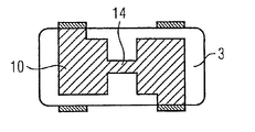
- FIG. 3 shows the section F—F of FIG. 1 .
- the electrode layer 3 of the second kind shown in FIG. 2 comprises a conductive layer 10 that connects the second pair 6 of external contacts to each other.
- the other elements shown in FIG. 3 match those shown in FIG. 2 .
- FIG. 4 shows the section F—F in a variant of FIG. 1 .
- the electrode layer 3 of the second kind shown in FIG. 4 has a conductive layer 10 with a narrow pass 14 located more or less in the middle.
- FIG. 5 shows the section F—F according to a variant of FIG. 1 .
- the electrode layer 3 of the second kind shown in FIG. 5 has a conductive layer 10 with two narrow passes 14 .
- FIG. 6 shows schematically a substitute circuit diagram for a component configured according to FIG. 1 , FIG. 2 and FIG. 3 .
- the electrode layers can be combined into a condenser C 1 by the parallel connection achieved with the help of external contacts.
- the connections A 1 to A 4 of FIG. 6 can be allocated to the external contacts 7 according to FIG. 2 as follows: A 1 corresponds to the external contact 7 in the upper left, A 2 corresponds to the external contact 7 in the lower left, A 3 corresponds to the external contact 7 in the upper right, and A 4 corresponds to the external contact 7 in the lower right.
- FIG. 7 shows an example of a further component according to the invention with two capacitances in the schematic longitudinal section.
- the elements shown correspond to the ones in FIG. 1 .
- the difference to FIG. 1 is that the conductive layers of the electrode layers 2 , 3 have different shapes.
- the electrode layers 2 of the first kind can be executed in a way as shown in FIG. 2 according to the section D—D.
- the conductive layer 9 shown in FIG. 2 can also be a layer made of a resistance paste.
- FIG. 8 shows the section E—E of FIG. 7 .
- the electrode layer 3 of the second kind shown in FIG. 8 comprises a conductive layer 10 and a conductive layer 101 , both of which are conductively connected from the external contacts 7 with an external contact 7 of the second pair 5 .
- a component with two capacitances can be achieved by configuring the electrode layer 3 of the second kind according to FIG. 8 , whereby the conductive layers 10 and 101 belong to different capacitances.
- the conductive layers 10 and 101 have approximately the same area, giving also the two capacitances about the same magnitudes.
- FIG. 9 shows the section E—E of a variant of FIG. 7 .
- the electrode layer 3 of the second kind shown in FIG. 9 comprises two conductive layers 10 , 101 , which are connected to the first pair 5 of external contacts.
- the conductive layers 10 and 101 have noticeably different areas, making it possible to achieve a multi-layered component with two different capacitances.
- FIG. 10 shows an example of a schematic substitute circuit diagram for a component according to FIG. 7 .
- the two capacitances C 1 and C 2 are connected in parallel to each other.
- the allocation of the connections A 1 to A 4 occurs in the same manner as described in FIG. 6 .
- FIG. 11 shows the section D—D in a variant of FIG. 7 .
- the electrode layer 2 of the first kind shown in FIG. 11 has a conductive layer 9 connected to an external contact 7 of the first pair 5 from external contacts 7 .
- the electrode layer 2 of the second kind also has a conductive layer 11 connected to the other external contact 7 of the first pair 5 .
- the conductive layers 9 , 11 are connected with each other through a resistance layer 12 .
- a ⁇ circuit can be achieved as shown in FIG. 13 , in which two capacitances C 1 and C 2 are connected to each other through a resistance R.
- FIG. 12 shows the section D—D of FIG. 7 for a variant of the component according to the invention.
- the electrode layer 2 of the first kind shown in FIG. 12 has a resistance layer 13 that connects the external contacts 7 of the first pair 5 with each other. Contrary to the arrangement of the electrode layer 2 of the first kind shown in FIG. 11 , the conductive layer is entirely dispensed with. A ir filter with a resistance connecting two capacitances can be achieved, also according to FIG. 12 .
- FIG. 12 shows a component according to FIG. 7 as seen from above.
- a resistance layer 13 is applied to the upper surface of the foundation 1 that connects the first pair 5 of external contacts 7 to each other.
- the variant to FIG. 11 shown in FIG. 12 can, in the same way as resistance paste applied on the inside of the component, be used to achieve a ⁇ filter according to FIG. 13 .
- FIG. 15 shows an insertion attenuation of the component shown in FIG. 14 .
- the insertion attenuation S is applied via the frequency f.
- the two resonance frequencies, f1, f2, as defined through both C 1 , C 2 capacitances, show an increased attenuation.
- the component shows a very good attenuation also between the resonance frequencies f1, f2 because of the resistance R implementing the ⁇ circuit, making the component suitable for noise suppression in a frequency band that lies between the resonance frequencies f1 (belongs to C 1 ) and the resonance frequency f2 (belongs to C 2 ).
- the capacitances C 1 and C 2 define the resonance frequencies f1 and f2 respectively, which are shown in FIG. 15 .
- FIG. 16 shows a noise suppression circuit according to the invention as seen from above.
- a first component 15 according to the invention and a second component 16 according to the invention are located on a circuit board 17 .
- the external contacts 7 of the components 15 , 16 are located along three parallel straight lines. Two external contacts 7 each are located along the outer straight line. Four external contacts 7 are located along the straight line in the middle.
- Circuit paths 18 run on the circuit board 17 along the straight line in the middle.
- the lower circuit paths 18 on the left and the upper circuit paths 18 on the right are executed as ground wire 19 .
- the ground wire 19 crosses the two other circuit paths 18 .
- the arrangement shown in FIG. 16 has the advantage that it is very compact and that the ground wire 19 can be placed at the edge of the group of circuit paths 18 .
Landscapes
- Engineering & Computer Science (AREA)
- Power Engineering (AREA)
- Manufacturing & Machinery (AREA)
- Microelectronics & Electronic Packaging (AREA)
- Fixed Capacitors And Capacitor Manufacturing Machines (AREA)
- Thermistors And Varistors (AREA)
- Superconductors And Manufacturing Methods Therefor (AREA)
- Coils Or Transformers For Communication (AREA)
Applications Claiming Priority (3)
| Application Number | Priority Date | Filing Date | Title |
|---|---|---|---|
| DE10064447.3 | 2000-12-22 | ||
| DE10064447A DE10064447C2 (de) | 2000-12-22 | 2000-12-22 | Elektrisches Vielschichtbauelement und Entstörschaltung mit dem Bauelement |
| PCT/DE2001/004591 WO2002052614A1 (de) | 2000-12-22 | 2001-12-06 | Elektrisches vielschichtbauelement und entstörschaltung mit dem bauelement |
Publications (2)
| Publication Number | Publication Date |
|---|---|
| US20040114305A1 US20040114305A1 (en) | 2004-06-17 |
| US6850404B2 true US6850404B2 (en) | 2005-02-01 |
Family
ID=7668573
Family Applications (1)
| Application Number | Title | Priority Date | Filing Date |
|---|---|---|---|
| US10/451,051 Expired - Fee Related US6850404B2 (en) | 2000-12-22 | 2001-12-06 | Component and interference suppression circuit |
Country Status (8)
| Country | Link |
|---|---|
| US (1) | US6850404B2 (de) |
| EP (1) | EP1350257B1 (de) |
| JP (1) | JP2004516676A (de) |
| CN (1) | CN1481564A (de) |
| AT (1) | ATE300091T1 (de) |
| DE (2) | DE10064447C2 (de) |
| TW (1) | TW575886B (de) |
| WO (1) | WO2002052614A1 (de) |
Cited By (12)
| Publication number | Priority date | Publication date | Assignee | Title |
|---|---|---|---|---|
| US20050180091A1 (en) * | 2004-01-13 | 2005-08-18 | Avx Corporation | High current feedthru device |
| US20060018081A1 (en) * | 2004-07-20 | 2006-01-26 | Samsung Electro-Mechanics Co., Ltd. | Laminated ceramic capacitor |
| US20060104002A1 (en) * | 2002-09-09 | 2006-05-18 | Gunter Engel | Multiple resonance filter |
| US20060158827A1 (en) * | 2005-01-20 | 2006-07-20 | Samsung Electro-Mechanics Co., Ltd. | Multilayer chip capacitor |
| US20080074826A1 (en) * | 2006-09-22 | 2008-03-27 | Samsung Electro-Mechanics Co., Ltd. | Multilayer chip capacitor |
| US20080165468A1 (en) * | 2007-01-05 | 2008-07-10 | Avx Corporation | Very low profile multilayer components |
| US20080239616A1 (en) * | 2007-03-30 | 2008-10-02 | Tdk Corporation | Multilayer capacitor array |
| US20080304202A1 (en) * | 2007-06-04 | 2008-12-11 | Taiyo Yuden Co., Ltd. | Multi-layer capacitor and integrated circuit module |
| US20090052113A1 (en) * | 2007-08-23 | 2009-02-26 | Tdk Corporation | Multilayer capacitor |
| US20100033896A1 (en) * | 2008-08-11 | 2010-02-11 | Tdk Corporation | Multilayer capacitor |
| US20100084738A1 (en) * | 2007-03-08 | 2010-04-08 | Koichiro Masuda | Capacitance element, printed circuit board, semiconductor package, and semiconductor circuit |
| US20160343510A1 (en) * | 2015-05-19 | 2016-11-24 | Beijing Yuan Liu Hong Yuan Electronic Technology Co., Ltd. | Capacitor With Various Capacitances |
Families Citing this family (10)
| Publication number | Priority date | Publication date | Assignee | Title |
|---|---|---|---|---|
| DE10144364A1 (de) | 2001-09-10 | 2003-04-03 | Epcos Ag | Elektrisches Vielschichtbauelement |
| DE10235011A1 (de) * | 2002-07-31 | 2004-02-26 | Epcos Ag | Elektrisches Vielschichtbauelement |
| AU2003264022A1 (en) * | 2002-08-07 | 2004-02-25 | Dearborn Electronics, Inc. | Improved electromagnetic interference filter |
| US6992387B2 (en) * | 2003-06-23 | 2006-01-31 | Intel Corporation | Capacitor-related systems for addressing package/motherboard resonance |
| TWI270195B (en) * | 2003-07-30 | 2007-01-01 | Innochips Technology | Complex laminated chip element |
| DE10356498A1 (de) * | 2003-12-03 | 2005-07-07 | Epcos Ag | Elektrisches Bauelement und Schaltungsanordnung |
| DE102004004096A1 (de) * | 2004-01-27 | 2005-08-18 | Epcos Ag | Elektrisches Vielschichtbauelement |
| TWI260097B (en) * | 2005-01-19 | 2006-08-11 | Via Tech Inc | Interconnection structure through passive component |
| DE102006013227A1 (de) * | 2005-11-11 | 2007-05-16 | Epcos Ag | Elektrisches Vielschichtbauelement |
| DE102009007316A1 (de) * | 2009-02-03 | 2010-08-05 | Epcos Ag | Elektrisches Vielschichtbauelement |
Citations (16)
| Publication number | Priority date | Publication date | Assignee | Title |
|---|---|---|---|---|
| JPH01107511A (ja) | 1987-10-20 | 1989-04-25 | Murata Mfg Co Ltd | 3端子型複合機能素子 |
| JPH0438810A (ja) | 1990-06-04 | 1992-02-10 | Hitachi Ltd | 4端子型コンデンサ |
| DE4342818A1 (de) | 1992-12-26 | 1994-06-30 | Murata Manufacturing Co | Zusammengesetztes elektronisches Bauteil |
| US5430605A (en) | 1992-08-04 | 1995-07-04 | Murata Erie North America, Inc. | Composite multilayer capacitive device and method for fabricating the same |
| DE19634498A1 (de) | 1996-08-26 | 1998-03-05 | Siemens Matsushita Components | Elektro-keramisches Bauelement und Verfahren zu seiner Herstellung |
| DE19639947A1 (de) | 1996-09-27 | 1998-04-16 | Siemens Matsushita Components | Passives Netzwerk in Chip-Bauform |
| EP0865053A2 (de) | 1997-02-26 | 1998-09-16 | Ngk Spark Plug Co., Ltd. | Mikroelektronische mehrschichtige Leiterplatte mit trimmbaren Kondensatoren |
| US5815367A (en) | 1996-03-11 | 1998-09-29 | Murata Manufacturing Co., Ltd. | Layered capacitors having an internal inductor element |
| US5870273A (en) | 1996-10-18 | 1999-02-09 | Tdk Corporation | Multi-functional multilayer device and method for making |
| US5880925A (en) | 1997-06-27 | 1999-03-09 | Avx Corporation | Surface mount multilayer capacitor |
| US5889445A (en) * | 1997-07-22 | 1999-03-30 | Avx Corporation | Multilayer ceramic RC device |
| EP0936642A2 (de) | 1998-02-09 | 1999-08-18 | Matsushita Electric Industrial Co., Ltd. | Kondensator met vier Anschlüssen |
| JPH11251178A (ja) | 1998-03-04 | 1999-09-17 | Taiyo Yuden Co Ltd | 4端子型積層コンデンサ |
| JPH11288846A (ja) | 1998-02-09 | 1999-10-19 | Matsushita Electric Ind Co Ltd | 4端子コンデンサ |
| DE19931056A1 (de) | 1999-07-06 | 2001-01-25 | Epcos Ag | Vielschichtvaristor niedriger Kapazität |
| US20010035810A1 (en) | 2000-03-30 | 2001-11-01 | Heistand Robert H. | Electronic device and process of making electronic device |
Family Cites Families (1)
| Publication number | Priority date | Publication date | Assignee | Title |
|---|---|---|---|---|
| US35810A (en) * | 1862-07-08 | Improved clothes-wringer |
-
2000
- 2000-12-22 DE DE10064447A patent/DE10064447C2/de not_active Expired - Fee Related
-
2001
- 2001-12-06 CN CNA018209890A patent/CN1481564A/zh active Pending
- 2001-12-06 EP EP01995584A patent/EP1350257B1/de not_active Expired - Lifetime
- 2001-12-06 WO PCT/DE2001/004591 patent/WO2002052614A1/de active IP Right Grant
- 2001-12-06 DE DE50106829T patent/DE50106829D1/de not_active Expired - Lifetime
- 2001-12-06 AT AT01995584T patent/ATE300091T1/de not_active IP Right Cessation
- 2001-12-06 JP JP2002553221A patent/JP2004516676A/ja not_active Withdrawn
- 2001-12-06 US US10/451,051 patent/US6850404B2/en not_active Expired - Fee Related
- 2001-12-18 TW TW090131313A patent/TW575886B/zh active
Patent Citations (16)
| Publication number | Priority date | Publication date | Assignee | Title |
|---|---|---|---|---|
| JPH01107511A (ja) | 1987-10-20 | 1989-04-25 | Murata Mfg Co Ltd | 3端子型複合機能素子 |
| JPH0438810A (ja) | 1990-06-04 | 1992-02-10 | Hitachi Ltd | 4端子型コンデンサ |
| US5430605A (en) | 1992-08-04 | 1995-07-04 | Murata Erie North America, Inc. | Composite multilayer capacitive device and method for fabricating the same |
| DE4342818A1 (de) | 1992-12-26 | 1994-06-30 | Murata Manufacturing Co | Zusammengesetztes elektronisches Bauteil |
| US5815367A (en) | 1996-03-11 | 1998-09-29 | Murata Manufacturing Co., Ltd. | Layered capacitors having an internal inductor element |
| DE19634498A1 (de) | 1996-08-26 | 1998-03-05 | Siemens Matsushita Components | Elektro-keramisches Bauelement und Verfahren zu seiner Herstellung |
| DE19639947A1 (de) | 1996-09-27 | 1998-04-16 | Siemens Matsushita Components | Passives Netzwerk in Chip-Bauform |
| US5870273A (en) | 1996-10-18 | 1999-02-09 | Tdk Corporation | Multi-functional multilayer device and method for making |
| EP0865053A2 (de) | 1997-02-26 | 1998-09-16 | Ngk Spark Plug Co., Ltd. | Mikroelektronische mehrschichtige Leiterplatte mit trimmbaren Kondensatoren |
| US5880925A (en) | 1997-06-27 | 1999-03-09 | Avx Corporation | Surface mount multilayer capacitor |
| US5889445A (en) * | 1997-07-22 | 1999-03-30 | Avx Corporation | Multilayer ceramic RC device |
| EP0936642A2 (de) | 1998-02-09 | 1999-08-18 | Matsushita Electric Industrial Co., Ltd. | Kondensator met vier Anschlüssen |
| JPH11288846A (ja) | 1998-02-09 | 1999-10-19 | Matsushita Electric Ind Co Ltd | 4端子コンデンサ |
| JPH11251178A (ja) | 1998-03-04 | 1999-09-17 | Taiyo Yuden Co Ltd | 4端子型積層コンデンサ |
| DE19931056A1 (de) | 1999-07-06 | 2001-01-25 | Epcos Ag | Vielschichtvaristor niedriger Kapazität |
| US20010035810A1 (en) | 2000-03-30 | 2001-11-01 | Heistand Robert H. | Electronic device and process of making electronic device |
Cited By (20)
| Publication number | Priority date | Publication date | Assignee | Title |
|---|---|---|---|---|
| US20060104002A1 (en) * | 2002-09-09 | 2006-05-18 | Gunter Engel | Multiple resonance filter |
| US7403083B2 (en) | 2002-09-09 | 2008-07-22 | Epcos Ag | Multiple resonance filter |
| US20050180091A1 (en) * | 2004-01-13 | 2005-08-18 | Avx Corporation | High current feedthru device |
| US20060018081A1 (en) * | 2004-07-20 | 2006-01-26 | Samsung Electro-Mechanics Co., Ltd. | Laminated ceramic capacitor |
| US7046500B2 (en) * | 2004-07-20 | 2006-05-16 | Samsung Electro-Mechanics Co., Ltd. | Laminated ceramic capacitor |
| US20060158827A1 (en) * | 2005-01-20 | 2006-07-20 | Samsung Electro-Mechanics Co., Ltd. | Multilayer chip capacitor |
| US7092236B2 (en) | 2005-01-20 | 2006-08-15 | Samsung Electro-Mechanics Co., Ltd. | Multilayer chip capacitor |
| US7545624B2 (en) * | 2006-09-22 | 2009-06-09 | Samsung Electro-Mechanics Co., Ltd. | Multilayer chip capacitor |
| US20080074826A1 (en) * | 2006-09-22 | 2008-03-27 | Samsung Electro-Mechanics Co., Ltd. | Multilayer chip capacitor |
| US20080165468A1 (en) * | 2007-01-05 | 2008-07-10 | Avx Corporation | Very low profile multilayer components |
| US20100084738A1 (en) * | 2007-03-08 | 2010-04-08 | Koichiro Masuda | Capacitance element, printed circuit board, semiconductor package, and semiconductor circuit |
| US8441774B2 (en) * | 2007-03-08 | 2013-05-14 | Nec Corporation | Capacitance element, printed circuit board, semiconductor package, and semiconductor circuit |
| US7675732B2 (en) * | 2007-03-30 | 2010-03-09 | Tdk Corporation | Multilayer capacitor array |
| US20080239616A1 (en) * | 2007-03-30 | 2008-10-02 | Tdk Corporation | Multilayer capacitor array |
| US20080304202A1 (en) * | 2007-06-04 | 2008-12-11 | Taiyo Yuden Co., Ltd. | Multi-layer capacitor and integrated circuit module |
| US20090052113A1 (en) * | 2007-08-23 | 2009-02-26 | Tdk Corporation | Multilayer capacitor |
| US7995325B2 (en) * | 2007-08-23 | 2011-08-09 | Tdk Corporation | Multilayer capacitor |
| US20100033896A1 (en) * | 2008-08-11 | 2010-02-11 | Tdk Corporation | Multilayer capacitor |
| US8068330B2 (en) * | 2008-08-11 | 2011-11-29 | Tdk Corporation | Multilayer capacitor |
| US20160343510A1 (en) * | 2015-05-19 | 2016-11-24 | Beijing Yuan Liu Hong Yuan Electronic Technology Co., Ltd. | Capacitor With Various Capacitances |
Also Published As
| Publication number | Publication date |
|---|---|
| JP2004516676A (ja) | 2004-06-03 |
| EP1350257A1 (de) | 2003-10-08 |
| DE50106829D1 (de) | 2005-08-25 |
| TW575886B (en) | 2004-02-11 |
| EP1350257B1 (de) | 2005-07-20 |
| US20040114305A1 (en) | 2004-06-17 |
| DE10064447C2 (de) | 2003-01-02 |
| WO2002052614A1 (de) | 2002-07-04 |
| ATE300091T1 (de) | 2005-08-15 |
| CN1481564A (zh) | 2004-03-10 |
| DE10064447A1 (de) | 2002-07-11 |
Similar Documents
| Publication | Publication Date | Title |
|---|---|---|
| US6850404B2 (en) | Component and interference suppression circuit | |
| US8179210B2 (en) | Electrical multilayer component with shielding and resistance structures | |
| CN101345134B (zh) | 层叠电容器 | |
| US7710233B2 (en) | Electric multilayer component | |
| US8659872B2 (en) | Multilayer capacitor that includes a capacitor element body and at least four terminal units | |
| US7710710B2 (en) | Electrical component and circuit configuration with the electrical component | |
| US20020044029A1 (en) | Surface mount RC devices | |
| JP4513855B2 (ja) | 積層コンデンサ | |
| US7646584B2 (en) | Multilayer feedthrough capacitor | |
| US7359178B2 (en) | Electrical functional unit | |
| US20110037559A1 (en) | Electrical multilayer component with reduced parasitic capacitance | |
| US20090207550A1 (en) | Electrical feedthrough component and method for its production | |
| JP2023169178A (ja) | 集積コンデンサフィルタおよびバリスタ機能を有する集積コンデンサフィルタ | |
| US20200343051A1 (en) | Integrated Component Including a Capacitor and Discrete Varistor | |
| KR101051620B1 (ko) | 적층 콘덴서 | |
| JPH07272975A (ja) | 複合コンデンサ | |
| US20230238186A1 (en) | Low Inductance Component | |
| KR101051621B1 (ko) | 관통 콘덴서 및 관통 콘덴서의 실장 구조 | |
| WO2018043397A1 (ja) | 積層型コンデンサ | |
| EP0841671A2 (de) | Elektronikbauteile mit Kondensatoren | |
| JP4412386B2 (ja) | 貫通型積層コンデンサ | |
| JP6662229B2 (ja) | 積層貫通コンデンサ及び電子部品装置 | |
| JPH0619314U (ja) | ノイズフィルタ |
Legal Events
| Date | Code | Title | Description |
|---|---|---|---|
| AS | Assignment |
Owner name: EPCOS AG, GERMANY Free format text: ASSIGNMENT OF ASSIGNORS INTEREST;ASSIGNORS:ENGEL, GUNTER;GREIER, GUNTHER;WITTMER, WALTER;REEL/FRAME:014895/0358;SIGNING DATES FROM 20030701 TO 20030809 |
|
| CC | Certificate of correction | ||
| FEPP | Fee payment procedure |
Free format text: PAYOR NUMBER ASSIGNED (ORIGINAL EVENT CODE: ASPN); ENTITY STATUS OF PATENT OWNER: LARGE ENTITY |
|
| FPAY | Fee payment |
Year of fee payment: 4 |
|
| FPAY | Fee payment |
Year of fee payment: 8 |
|
| REMI | Maintenance fee reminder mailed | ||
| LAPS | Lapse for failure to pay maintenance fees | ||
| STCH | Information on status: patent discontinuation |
Free format text: PATENT EXPIRED DUE TO NONPAYMENT OF MAINTENANCE FEES UNDER 37 CFR 1.362 |
|
| FP | Lapsed due to failure to pay maintenance fee |
Effective date: 20170201 |