US6833696B2 - Methods and apparatus for creating a high speed connection between a device under test and automatic test equipment - Google Patents
Methods and apparatus for creating a high speed connection between a device under test and automatic test equipment Download PDFInfo
- Publication number
- US6833696B2 US6833696B2 US10/725,966 US72596603A US6833696B2 US 6833696 B2 US6833696 B2 US 6833696B2 US 72596603 A US72596603 A US 72596603A US 6833696 B2 US6833696 B2 US 6833696B2
- Authority
- US
- United States
- Prior art keywords
- assembly
- dut
- contacts
- spine
- assemblies
- Prior art date
- Legal status (The legal status is an assumption and is not a legal conclusion. Google has not performed a legal analysis and makes no representation as to the accuracy of the status listed.)
- Expired - Lifetime
Links
Images


Classifications
-
- G—PHYSICS
- G01—MEASURING; TESTING
- G01R—MEASURING ELECTRIC VARIABLES; MEASURING MAGNETIC VARIABLES
- G01R31/00—Arrangements for testing electric properties; Arrangements for locating electric faults; Arrangements for electrical testing characterised by what is being tested not provided for elsewhere
- G01R31/28—Testing of electronic circuits, e.g. by signal tracer
- G01R31/2851—Testing of integrated circuits [IC]
- G01R31/2886—Features relating to contacting the IC under test, e.g. probe heads; chucks
- G01R31/2889—Interfaces, e.g. between probe and tester
-
- G—PHYSICS
- G01—MEASURING; TESTING
- G01R—MEASURING ELECTRIC VARIABLES; MEASURING MAGNETIC VARIABLES
- G01R31/00—Arrangements for testing electric properties; Arrangements for locating electric faults; Arrangements for electrical testing characterised by what is being tested not provided for elsewhere
- G01R31/28—Testing of electronic circuits, e.g. by signal tracer
- G01R31/317—Testing of digital circuits
- G01R31/3181—Functional testing
- G01R31/319—Tester hardware, i.e. output processing circuits
- G01R31/31903—Tester hardware, i.e. output processing circuits tester configuration
- G01R31/31905—Interface with the device under test [DUT], e.g. arrangements between the test head and the DUT, mechanical aspects, fixture
-
- G—PHYSICS
- G01—MEASURING; TESTING
- G01R—MEASURING ELECTRIC VARIABLES; MEASURING MAGNETIC VARIABLES
- G01R31/00—Arrangements for testing electric properties; Arrangements for locating electric faults; Arrangements for electrical testing characterised by what is being tested not provided for elsewhere
- G01R31/28—Testing of electronic circuits, e.g. by signal tracer
- G01R31/282—Testing of electronic circuits specially adapted for particular applications not provided for elsewhere
- G01R31/2822—Testing of electronic circuits specially adapted for particular applications not provided for elsewhere of microwave or radiofrequency circuits
Definitions
- the present invention relates to techniques for reliably creating a large number of high-speed electrical connections between two circuits. More specifically, the present invention provides a variety of techniques for establishing such connections with a high cycle life while requiring a very low externally-created force to facilitate the connect-disconnect cycle.
- a device-under test (DUT) assembly includes a DUT board having a plurality of spine assemblies disposed thereon out of the plane of the DUT board. Each spine assembly has a first outer face, a second outer face, and a first plurality of contacts on at least one of the first and second outer faces in electrical contact with a subset of the first signal lines.
- the DUT assembly also includes a first mechanical alignment feature.
- a connector assembly includes a plurality of clamping assemblies corresponding to and arranged to receive the plurality of spine assemblies.
- Each clamping assembly includes a first inner face, a second inner face substantially parallel to the first inner face, and a second plurality of contacts on at least one of the first and second inner faces in electrical contact with a subset of the second signal lines.
- Each clamping assembly is independently suspended within the connector assembly and includes a second mechanical alignment feature. The second contacts of each clamping assembly align with the first contacts of the corresponding spine assembly through interaction of the first and second mechanical alignment features. Electrical connections between the first and second contacts are formed when the first and second inner faces of each clamping assembly are clamped to the first and second outer faces of the corresponding spine assembly, thereby electrically connecting the first and second signal lines.
- a device-under test (DUT) assembly includes a plurality of DUT boards. Each DUT board has a first outer face at an end and on one side of the DUT board, a second outer face at the end and on the other side of the DUT board, and a first plurality of contacts on at least one of the first and second outer faces in electrical contact with a subset of the first signal lines.
- the DUT assembly also includes a first mechanical alignment feature.
- a connector assembly includes a plurality of clamping assemblies corresponding to and arranged to receive the ends of the plurality of DUT boards.
- Each clamping assembly has a first inner face, a second inner face substantially parallel to the first inner face, and a second plurality of contacts on at least one of the first and second inner faces in electrical contact with a subset of the second signal lines.
- Each clamping assembly is independently suspended within the connector assembly and includes a second mechanical alignment feature. The second contacts of each clamping assembly align with the first contacts of the corresponding DUT board through interaction of the first and second mechanical alignment features. Electrical connections between the first and second contacts are formed when the first and second inner faces of each clamping assembly are clamped to the first and second outer faces of the corresponding DUT board, thereby electrically connecting the first and second signal lines.
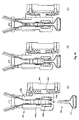
- FIG. 1 shows a device under test (DUT) printed circuit board assembly and a corresponding tower assembly designed according to a specific embodiment of the invention.
- DUT device under test
- FIG. 2 is a closer view of the DUT assembly of FIG. 1 .
- FIG. 3 is still a closer view of the DUT assembly of FIG. 1 showing detailed features of the plurality of spine assemblies disposed thereon.
- FIG. 4 is a closer view of the tower assembly of FIG. 1 .
- FIG. 5 is still a closer view of the tower assembly of FIG. 1 illustrating the mechanism by which the tower assembly is secured to and aligned with the DUT assembly.
- FIG. 6 is an even closer view of the tower assembly of FIG. 1 showing detailed features of the plurality of clamping assemblies of which the tower assembly is comprised.
- FIG. 7 is a view of the opposite side of the tower assembly.
- FIG. 8 is a closer view of the side of the tower assembly shown in FIG. 7 in which the interface between signal lines and the clamping assemblies is shown.
- FIG. 9 is a view of the system in which the clamping assemblies and the corresponding spine assemblies are aligned.
- FIG. 10 is a cutaway view of the lifting and alignment mechanisms corresponding to the position of FIG. 9 .
- FIG. 11 is a view of the system in which the clamping assemblies and the corresponding spine assemblies are in a pre-docking position.
- FIG. 12 is a cutaway view of the lifting and alignment mechanisms corresponding to the position of FIG. 11 .
- FIG. 13 is a view of the system in which the clamping assemblies and the corresponding spine assemblies are docked.
- FIG. 14 is a cutaway view of the lifting and alignment mechanisms corresponding to the position of FIG. 13 .
- FIG. 15 is a view of the system in which the clamping assemblies are clamped onto the corresponding spine assemblies.
- FIGS. 16A-16C show a perspective view of a clamping assembly and a spine assembly at various stages of the docking process.
- FIGS. 17A-17C show a first end-on view of a clamping assembly and a spine assembly at various stages of the docking process.
- FIGS. 18A-18C show a second end-on view of a clamping assembly and a spine assembly at various stages of the docking process.
- FIGS. 19A-19C show a cross-section view of a clamping assembly and a spine assembly at various stages of the docking process.
- FIG. 20 shows how the tower assembly of FIG. 1 may be connected to the test electronics according to a specific embodiment of the invention.
- a DUT assembly 102 is provided on the underside of which are a large number of electrical contacts (not shown) to one or more DUTs.
- Such electrical contacts might be, for example, probe needles if DUT assembly 102 is probe card for use in wafer sort, or sockets if DUT board 102 is a contactor board for use in package test.
- the primary function of DUT assembly 102 is to translate electrical signals out of the plane of board 104 so that they are accessible to the connection mechanism, i.e., interface tower assembly 106 .
- DUT assembly 102 has a plurality of “spine” structures 202 disposed radially on board 104 which facilitate the signal translation.
- spines 202 A specific implementation of spines 202 is shown in FIG. 3 .
- Each spine 202 comprises a rigid support assembly 302 which includes fine alignment slots 304 and 305 .
- a flex circuit 306 fastened to and supported by assembly 302 includes signal traces (not shown) which transmit signals between contacts 308 at the bottom of assembly 302 to contacts 310 on either side of assembly 302 .
- Contacts 308 mate with corresponding contacts (not shown) on the surface of board 104 when spine 202 is secured in place.
- support assembly 302 may include flexible material 312 disposed as shown in assembly 302 which provide contact backup for contacts 308 .
- similar contact backup may be provided for contacts 310 . While embodiments are contemplated in which such contact backup is provided by the rigid material of which assembly 302 is constructed, the flexible nature of material 312 ensures that the electrical connections made with contacts 308 will have sufficient integrity despite any possible minor variations in contact height. That is, to make the connection reliable across the entire connection array, there may either be a compressible member in the system, or the flatness tolerance of the components may be controlled to a very tight tolerance.
- the compressible member is a piece of silicone rubber inserted into the spine behind the contacts.
- the compressible member is a piece of silicone rubber that backs up each of the flexible circuits which clamp down onto the connections on the spine.
- the clamping mechanism itself doubles as the flexible/compressible member. That is, silicone or urethane (i.e., elastomeric) flexible bladders bear directly on the back of the flexible circuits and expand to create the required compressive force.
- DUT assembly 102 includes a central assembly 204 which includes features by which the initial alignment of assembly 102 to assembly 106 may be achieved. That is, assembly 204 includes a central lifting point 206 by which DUT assembly 102 may be moved up and down.
- kinematic couple alignment channels defined by cylindrical shafts 208 are provided which correspond to kinematic structures on tower assembly 106 (described below) and which facilitate securing of the relative positions of DUT assembly 102 and tower assembly 106 when the two assemblies are engaged with each other. More on the nature of this kinematic coupling will be described below.
- board 104 is not restricted to the circular geometry shown in the figures. Rather, any shape suitable for the particular application, e.g., rectangular, may be employed.
- configuration of the spines need not be as shown. That is, for example, rather than the radial distribution depicted in FIGS. 1-3, the spines may be distributed in a rectilinear distribution. As a practical matter, any distribution of spines or equivalent structures as appropriate for a particular application may be employed.
- the structure of the spines themselves may vary considerably without departing from the scope of the invention.
- signal traces could be integral to the support structure itself which might comprise, for example, a printed circuit board. Any physical structure which can translate signals out of the plane of the DUT board may be employed for this aspect of the invention.
- interface tower assembly 106 includes a plurality of clamping connector assemblies 402 radially disposed on tower assembly frame 404 .
- the radial pattern shown is merely exemplary.
- connector assemblies 402 may be disposed in as many different ways as spines 202 and, in fact, must correspond to the distribution of spines on the associated DUT assembly.
- Each connector assembly 402 corresponds to one of spines 202 on DUT assembly 102 .
- each of spines 202 fits into a corresponding connector assembly 402 , the inner walls of which have electrical contacts which correspond to and make connections with contacts 310 on flex circuit 306 .
- a pneumatically powered latch 502 receives lifting point 206 on DUT assembly 102 and pulls spring loaded kinematic alignment balls 504 into contact with kinematic alignment shafts 208 on the DUT assembly.
- springs see FIGS. 10, 12 , and 14
- balls 504 also come into contact with kinematic alignment shafts 508 on assembly 106 .
- This kinematic arrangement resolves all six degrees of freedom, thereby inhibiting relative motion between DUT assembly 102 and tower assembly 106 . It will be understood that the kinematic system illustrated in these figures is only one of many possible mechanisms which may be employed for this purpose.
- FIG. 6 shows a closer view of a portion of an interface tower assembly 106 in which contacts 602 on the inner walls of connector assemblies 402 are apparent.
- the connection between contacts 602 and the corresponding contacts 310 on spine assemblies 202 are facilitated by air cylinders 604 which, once spines 202 are inserted into connector assemblies 402 , force the opposing walls (i.e., connection boards 606 ) of each assembly 402 against the opposing sides of the corresponding spine 202 .
- Press plates 608 are provided to ensure an even distribution of the force exerted by air cylinders 604 across connection boards 606 .
- the clamping force is exerted via shafts 612 which extend from cylinder 604 through the near plate and are secured to the opposite side plate.
- clamping cylinders 604 may be replaced with other mechanisms such as, for example, expandable cylinders or bladders made of silicone or urethane.
- contacts 308 , 310 , and 602 may be implemented in a variety of ways. That is, the term “contacts” has been used in the foregoing description to generically refer to a conductor termination which may form an electrical connection with another conductor termination, e.g., pads and bumps. It will be understood that the specific type of contact employed is immaterial as long as sufficient connective integrity is maintained for the particular application.
- FIG. 6 also shows springs 610 which work to keep connection boards 606 apart against the action of clamping cylinders 604 . Thus, in the event of the loss of air pressure, clamping connector assemblies 402 will automatically open. According to alternative embodiments, elastic spacers may be used to perform this function.
- FIG. 7 shows tower assembly 106 from the opposite side of previous views.
- Air cylinder 702 powers latch 502 .
- Emergency brake 704 which requires air pressure to be released ensures that once assemblies 102 and 106 are secured together they remain together even if there is a loss of power and/or air pressure.
- power is removed from air cylinder 702 , and brake 704 is engaged, thereby making disengagement of the assemblies virtually impossible without reapplication of power.
- connection boards 606 can be seen, attached to which are a plurality of shielded transmission lines 802 for routing a variety of high-speed signals to and from test boards associated with the automated test equipment (not shown).
- Unshielded conductors 804 are also shown which provide connection and utility signals to and from connection boards 606 .
- Air hoses 806 provide air pressure to clamping cylinders 604 .
- connection boards 606 and transmission lines 802 may be provided in a variety of ways without departing from the scope of the invention.
- connection boards 606 are implemented using flex circuits.
- both connection boards 606 and transmission lines 802 are replaced with a flex circuit which is designed as described in commonly assigned, copending U.S. patent application Ser. No. 10/365,262 for FLEX-CIRCUIT-BASED HIGH SPEED TRANSMISSION LINE filed on Feb. 11, 2003, the entire disclosure of which is incorporated herein by reference.
- the system described above may be used to provide repeatable connectivity for a wide variety of applications, some of which relate to the high-speed testing of semiconductor wafers or electronic circuits. It should also be understood that the parallelism represented by the system described above may be leveraged in a variety of ways to take full advantage of the invention. For example, most or all of the connectivity provided by such a system could be used to simultaneously test an entire wafer (e.g., 8 inches or larger). Alternatively, a large number of separate and distinct DUTs might be connected to each spine on the DUT assembly, allowing for the simultaneous testing and verification of hundreds of devices.
- a degree of “independent suspension” is provided for each of the clamping connector assemblies with respect to the tower assembly of which they are a part. This allows for some self-alignment of the clamping connector assemblies to the spines on the DUT assembly which, as will be discussed, both simplifies the overall design as well as ensures the reliable and repeatable alignment of the contacts on both assemblies.
- the manner in which this independent suspension is accomplished according to a specific embodiment of the invention will be described below with reference to FIGS. 16-19.
- FIGS. 9-15 illustrate the alignment, docking, and clamping functionalities of the embodiment of the invention described herein.
- Initial alignment between the tower assembly and the DUT assembly is achieved by inserting the DUT assembly's lifting point 206 into lifting point receiver 502 , and bringing kinematic alignment balls 504 on the tower assembly into contact with the kinematic alignment channels on the DUT assembly as shown in FIG. 10 . As shown in FIG. 9, this brings spine assemblies 202 into a coarse alignment with clamping connector assemblies 402 .
- spines 202 are brought into closer proximity with their corresponding connector assemblies 402 . As shown in FIG. 12, this is achieved when the DUT assembly has been lifted sufficiently such that the top of lifting point 206 is above latching balls 1202 . At this point, lifting point air cylinder 702 is energized, causing latching balls 1202 to be driven inward and under the top of lifting point 206 . Spring 1205 around shaft 1206 associated with each kinematic alignment ball 504 is compressed as shown, pushing the opposing end of shaft 1206 upward.
- each clamping connector assembly 402 has two shafts (shafts 612 of FIG. 6) which mate with the corresponding alignment slots 304 and 305 on spine 202 to achieve the docked position of FIG. 13 .
- clamping connector assemblies 402 are able to move independently in all axes, when these pairs of shafts are engaged, independent and precise alignment is achieved between the contacts on each spine 202 and the corresponding contacts on the connection boards or flex circuits of the associated clamping connector assembly 402 .
- this freedom of movement in combination with the local alignment mechanisms for each clamping connector/spine pair and the clamping action provided by the clamping devices compensates for minor variations in spine orientation with respect to any of x, y, z, pitch, roll, or yaw, thereby decreasing dependence on the kinematic system for aligning the contacts on every spine with the corresponding contacts on every clamping connector.
- FIG. 13 The docked position of FIG. 13 is achieved by the action of lifting point air cylinder 702 on lifting point 206 and the resulting action of the kinematic system. As shown in FIG. 14, air cylinder 702 lifts the DUT assembly until each kinematic alignment ball 504 stops further lifting by coming to rest against the bottom and top kinematic alignment channels (i.e., the channels defined by shafts 208 of FIG. 2 and shafts 508 of FIG. 5 ).
- the bottom and top kinematic alignment channels i.e., the channels defined by shafts 208 of FIG. 2 and shafts 508 of FIG. 5 .
- lifting point 206 (and therefore the DUT assembly) is being held in place at this point by the lifting action of the air cylinder which, because of the continuous pressure which maintains the kinematic alignment balls in the kinematic alignment grooves, maintains alignment between the DUT assembly and the tower assembly.
- FIGS. 16A-16C show isolated views of a clamping assembly 402 and a spine assembly 202 in relative positions corresponding to FIGS. 11, 13 , and 15 , respectively.
- Each plate 608 of clamping assembly 402 includes an elastomer grommet 1602 having flexible spokes centered on a plastic bushing 1604 through which a shaft 1606 extends.
- Grommets 1602 and bushings 1604 are able to slide along shaft 1606 which is secured in a corresponding groove at the outer edge of assembly 404 .
- Assembly 402 is secured to the inner edge of assembly 404 via urethane structure 1608 .
- the flexible natures of grommets 1602 and structure 1608 provide the independent suspension which, together with the local mechanical alignment features described above, enables the precise alignment of each individual pair of assemblies 202 and 402 .
- FIGS. 17A-17C and FIGS. 18A-18C show end-on views of the same isolated pair of assemblies in the various stages of docking.
- the views of FIG. 17 are from the outer edge of assembly 404 looking toward its center, and those of FIG. 18 are from the center looking out.
- Local alignment features 304 and 305 of assembly 202 engage the lower shafts 612 coupled to cylinder 604 (the one in FIG. 17A being obscured by shaft 1606 ), and effect the alignment of the electrical connections on the respective assemblies.
- FIGS. 17B and 18B the independent suspension of assembly 402 (most clearly illustrated in FIG. 17B by the deformation of flexible structure 1608 ) results in the assembly being raised up slightly with respect to its previous position in FIGS. 17A and 18A.
- structure 1608 is further deformed as clamping cylinder 604 causes assembly 402 to clamp onto assembly 202 .
- FIGS. 19A-19C provide cross-sectional views of the views of FIGS. 17A-17C.
- clamping cylinder 604 employs an inflatable bladder 1902 which, when inflated, pulls left plate 608 A and pushes right plate 608 B together via the action of shafts 612 extending through the right plate and attaching to the left.
- flexible material 1904 in plates 608 behind connection boards 606 to provide backing for the contacts on connection boards 606 . As discussed above with reference to FIG. 3, this ensures that the electrical connections made with the contacts on assembly 202 will have sufficient integrity despite any possible minor variations in contact height.
- clamping assembly 402 is shown clamped to one of spine assemblies 202 on DUT assembly 102 .
- Clamping assembly 402 is also connected back-to-back (via conductors 802 and 804 ) with another clamping assembly (not shown) which clamps onto one of test connection boards 2002 . This is accomplished in a manner similar to that described above with respect to the docking process between assemblies 202 and 402 .
- One such clamping assembly 2004 is shown having conductors 802 and 804 to which a clamping assembly 402 (not shown) is connected back-to-back.
- Test connection boards 2002 are either part of, or are connected to, one or more PE boards which carry signals to and from the test equipment. In this way, connections to the system test electronics are provided to the devices under test connected to DUT assembly 102 .
- the DUT assembly may comprise a plurality of vertically disposed DUT boards (e.g., printed circuit boards).
- the end of each board takes the place of one of the spines in the above-described embodiments.
- Each clamping assembly in the tower clamps on the end of a corresponding one of the vertical boards.
Landscapes
- Engineering & Computer Science (AREA)
- General Engineering & Computer Science (AREA)
- Physics & Mathematics (AREA)
- General Physics & Mathematics (AREA)
- Computer Hardware Design (AREA)
- Microelectronics & Electronic Packaging (AREA)
- Tests Of Electronic Circuits (AREA)
- Testing Or Measuring Of Semiconductors Or The Like (AREA)
- Coupling Device And Connection With Printed Circuit (AREA)
- Details Of Connecting Devices For Male And Female Coupling (AREA)
- Testing Of Individual Semiconductor Devices (AREA)
Priority Applications (8)
| Application Number | Priority Date | Filing Date | Title |
|---|---|---|---|
| US10/725,966 US6833696B2 (en) | 2003-03-04 | 2003-12-01 | Methods and apparatus for creating a high speed connection between a device under test and automatic test equipment |
| JP2006508868A JP2006523310A (ja) | 2003-03-04 | 2004-02-25 | 高速コネクタ |
| PCT/US2004/005858 WO2004079865A2 (en) | 2003-03-04 | 2004-02-25 | High speed connector |
| US10/965,245 US6963211B2 (en) | 2003-03-04 | 2004-10-13 | Methods and apparatus for creating a high speed connection between a device under test and automatic test equipment |
| US11/189,953 US7078890B2 (en) | 2003-03-04 | 2005-07-25 | Methods and apparatus for creating a high speed connection between a device under test and automatic test equipment |
| US11/479,354 US7358754B2 (en) | 2003-03-04 | 2006-06-30 | Methods and apparatus for creating a high speed connection between a device under test and automatic test equipment |
| US11/548,382 US20070126439A1 (en) | 2003-03-04 | 2006-10-11 | Methods and apparatus for creating a high speed connection between a device under test and automatic test equipment |
| JP2006329101A JP2007129245A (ja) | 2003-03-04 | 2006-12-06 | 高速コネクタ |
Applications Claiming Priority (2)
| Application Number | Priority Date | Filing Date | Title |
|---|---|---|---|
| US45219603P | 2003-03-04 | 2003-03-04 | |
| US10/725,966 US6833696B2 (en) | 2003-03-04 | 2003-12-01 | Methods and apparatus for creating a high speed connection between a device under test and automatic test equipment |
Related Child Applications (1)
| Application Number | Title | Priority Date | Filing Date |
|---|---|---|---|
| US10/965,245 Continuation US6963211B2 (en) | 2003-03-04 | 2004-10-13 | Methods and apparatus for creating a high speed connection between a device under test and automatic test equipment |
Publications (2)
| Publication Number | Publication Date |
|---|---|
| US20040174174A1 US20040174174A1 (en) | 2004-09-09 |
| US6833696B2 true US6833696B2 (en) | 2004-12-21 |
Family
ID=32930682
Family Applications (5)
| Application Number | Title | Priority Date | Filing Date |
|---|---|---|---|
| US10/725,966 Expired - Lifetime US6833696B2 (en) | 2003-03-04 | 2003-12-01 | Methods and apparatus for creating a high speed connection between a device under test and automatic test equipment |
| US10/965,245 Expired - Lifetime US6963211B2 (en) | 2003-03-04 | 2004-10-13 | Methods and apparatus for creating a high speed connection between a device under test and automatic test equipment |
| US11/189,953 Expired - Lifetime US7078890B2 (en) | 2003-03-04 | 2005-07-25 | Methods and apparatus for creating a high speed connection between a device under test and automatic test equipment |
| US11/479,354 Expired - Lifetime US7358754B2 (en) | 2003-03-04 | 2006-06-30 | Methods and apparatus for creating a high speed connection between a device under test and automatic test equipment |
| US11/548,382 Abandoned US20070126439A1 (en) | 2003-03-04 | 2006-10-11 | Methods and apparatus for creating a high speed connection between a device under test and automatic test equipment |
Family Applications After (4)
| Application Number | Title | Priority Date | Filing Date |
|---|---|---|---|
| US10/965,245 Expired - Lifetime US6963211B2 (en) | 2003-03-04 | 2004-10-13 | Methods and apparatus for creating a high speed connection between a device under test and automatic test equipment |
| US11/189,953 Expired - Lifetime US7078890B2 (en) | 2003-03-04 | 2005-07-25 | Methods and apparatus for creating a high speed connection between a device under test and automatic test equipment |
| US11/479,354 Expired - Lifetime US7358754B2 (en) | 2003-03-04 | 2006-06-30 | Methods and apparatus for creating a high speed connection between a device under test and automatic test equipment |
| US11/548,382 Abandoned US20070126439A1 (en) | 2003-03-04 | 2006-10-11 | Methods and apparatus for creating a high speed connection between a device under test and automatic test equipment |
Country Status (3)
| Country | Link |
|---|---|
| US (5) | US6833696B2 (https=) |
| JP (2) | JP2006523310A (https=) |
| WO (1) | WO2004079865A2 (https=) |
Cited By (15)
| Publication number | Priority date | Publication date | Assignee | Title |
|---|---|---|---|---|
| US20050159050A1 (en) * | 2003-06-05 | 2005-07-21 | Hiroyuki Hama | Device interface apparatus |
| US20060236495A1 (en) * | 2005-04-25 | 2006-10-26 | Romi Mayder | Method and apparatus for non-contact cleaning of electronics |
| US7147499B1 (en) | 2005-10-19 | 2006-12-12 | Verigy Ipco | Zero insertion force printed circuit assembly connector system and method |
| US20070176615A1 (en) * | 2006-01-27 | 2007-08-02 | Xandex, Inc. | Active probe contact array management |
| US20070296424A1 (en) * | 2006-05-31 | 2007-12-27 | Romi Mayder | Method and apparatus for a paddle board probe card |
| US20080139014A1 (en) * | 2006-12-08 | 2008-06-12 | Verigy (Singapore) Pte. Ltd. | Interconnect assemblies, and methods of forming interconnects |
| US20120206159A1 (en) * | 2011-02-11 | 2012-08-16 | Micron Technology, Inc. | Interface |
| WO2013009817A1 (en) | 2011-07-12 | 2013-01-17 | Intest Corporation | Method and apparatus for docking a test head with a peripheral |
| US10145893B2 (en) | 2016-12-25 | 2018-12-04 | Nuvoton Technology Corporation | Resolving automated test equipment (ATE) timing constraint violations |
| US10451652B2 (en) | 2014-07-16 | 2019-10-22 | Teradyne, Inc. | Coaxial structure for transmission of signals in test equipment |
| US10972192B2 (en) | 2018-05-11 | 2021-04-06 | Teradyne, Inc. | Handler change kit for a test system |
| US11604219B2 (en) | 2020-12-15 | 2023-03-14 | Teradyne, Inc. | Automatic test equipement having fiber optic connections to remote servers |
| US11855376B2 (en) | 2021-03-24 | 2023-12-26 | Teradyne, Inc. | Coaxial contact having an open-curve shape |
| US11862901B2 (en) | 2020-12-15 | 2024-01-02 | Teradyne, Inc. | Interposer |
| US12046787B2 (en) | 2021-05-14 | 2024-07-23 | Teradyne, Inc. | Waveguide connector for connecting first and second waveguides, where the connector includes a male part, a female part and a self-alignment feature and a test system formed therefrom |
Families Citing this family (10)
| Publication number | Priority date | Publication date | Assignee | Title |
|---|---|---|---|---|
| US6833696B2 (en) * | 2003-03-04 | 2004-12-21 | Xandex, Inc. | Methods and apparatus for creating a high speed connection between a device under test and automatic test equipment |
| US7161347B1 (en) * | 2005-07-08 | 2007-01-09 | Credence Systems Corporation | Test head for semiconductor integrated circuit tester |
| KR100962501B1 (ko) * | 2007-12-20 | 2010-06-14 | (주)케미텍 | 반도체 시험용 커넥터 어셈블리 |
| WO2010062967A2 (en) * | 2008-11-25 | 2010-06-03 | Verigy (Singapore) Pte. Ltd. | Test electronics to device under test interfaces, and methods and apparatus using same |
| WO2010117565A2 (en) * | 2009-04-09 | 2010-10-14 | Teradyne, Inc. | Automated test equipment employing test signal transmission channel with embedded series isolation resistors |
| KR100951919B1 (ko) | 2009-11-23 | 2010-04-09 | (주)케미텍 | 반도체 시험용 커넥터 어셈블리 |
| US8872532B2 (en) * | 2009-12-31 | 2014-10-28 | Formfactor, Inc. | Wafer test cassette system |
| CN103221833B (zh) * | 2010-10-29 | 2016-06-08 | 爱德万测试公司 | 具有专用电子模块的测试器和并入或使用该测试器的系统和方法 |
| KR101912710B1 (ko) | 2017-10-20 | 2018-12-28 | 주식회사 오킨스전자 | 낮은 삽입력을 가지는 커넥터 |
| CN111257717A (zh) * | 2020-03-03 | 2020-06-09 | 李鑫 | 一种pin二极管用检测装置 |
Citations (5)
| Publication number | Priority date | Publication date | Assignee | Title |
|---|---|---|---|---|
| US4589815A (en) | 1982-08-25 | 1986-05-20 | Intest Corporation | Electronic test head positioner for test systems |
| US5068601A (en) | 1991-02-11 | 1991-11-26 | Credence Systems Corporation | Dual function cam-ring system for DUT board parallel electrical inter-connection and prober/handler docking |
| US5552701A (en) | 1995-05-15 | 1996-09-03 | Hewlett-Packard Company | Docking system for an electronic circuit tester |
| US5923180A (en) | 1997-02-04 | 1999-07-13 | Hewlett-Packard Company | Compliant wafer prober docking adapter |
| US6040691A (en) * | 1997-05-23 | 2000-03-21 | Credence Systems Corporation | Test head for integrated circuit tester arranging tester component circuit boards on three dimensions |
Family Cites Families (20)
| Publication number | Priority date | Publication date | Assignee | Title |
|---|---|---|---|---|
| US4613193A (en) * | 1984-08-13 | 1986-09-23 | Tritec, Inc. | Board-operated electrical connector for printed circuit boards |
| US4911643A (en) * | 1988-10-11 | 1990-03-27 | Beta Phase, Inc. | High density and high signal integrity connector |
| US4969824A (en) * | 1989-07-28 | 1990-11-13 | Amp Incorporated | Electrical connector |
| JPH04109645A (ja) * | 1990-08-30 | 1992-04-10 | Sumitomo Electric Ind Ltd | 半導体プロービング試験装置 |
| JPH04109646A (ja) * | 1990-08-30 | 1992-04-10 | Sumitomo Electric Ind Ltd | 半導体プロービング試験装置 |
| US5092781A (en) * | 1990-11-08 | 1992-03-03 | Amp Incorporated | Electrical connector using shape memory alloy coil springs |
| KR100248569B1 (ko) * | 1993-12-22 | 2000-03-15 | 히가시 데쓰로 | 프로우브장치 |
| TW273635B (https=) * | 1994-09-01 | 1996-04-01 | Aesop | |
| TW298686B (https=) * | 1995-04-25 | 1997-02-21 | Hitachi Ltd | |
| SG55211A1 (en) * | 1995-07-05 | 1998-12-21 | Tokyo Electron Ltd | Testing apparatus |
| US5679018A (en) * | 1996-04-17 | 1997-10-21 | Molex Incorporated | Circuit card connector utilizing flexible film circuitry |
| US5861759A (en) * | 1997-01-29 | 1999-01-19 | Tokyo Electron Limited | Automatic probe card planarization system |
| US6004142A (en) * | 1997-03-04 | 1999-12-21 | Micron Technology, Inc. | Interposer converter to allow single-sided contact to circuit modules |
| US5986447A (en) * | 1997-05-23 | 1999-11-16 | Credence Systems Corporation | Test head structure for integrated circuit tester |
| US6064195A (en) * | 1998-05-11 | 2000-05-16 | R-Tec Corporation | Test probe positioning device |
| DE19931337A1 (de) * | 1998-07-09 | 2000-01-27 | Advantest Corp | Befestigungsvorrichtung für Halbleiter-Bauelemente |
| DE10039336C2 (de) * | 2000-08-04 | 2003-12-11 | Infineon Technologies Ag | Verfahren zum Testen von Halbleiterschaltungen und Testvorrichtung zur Durchführung des Verfahrens |
| US6762612B2 (en) * | 2001-06-20 | 2004-07-13 | Advantest Corp. | Probe contact system having planarity adjustment mechanism |
| US6833696B2 (en) * | 2003-03-04 | 2004-12-21 | Xandex, Inc. | Methods and apparatus for creating a high speed connection between a device under test and automatic test equipment |
| US7068056B1 (en) * | 2005-07-18 | 2006-06-27 | Texas Instruments Incorporated | System and method for the probing of a wafer |
-
2003
- 2003-12-01 US US10/725,966 patent/US6833696B2/en not_active Expired - Lifetime
-
2004
- 2004-02-25 WO PCT/US2004/005858 patent/WO2004079865A2/en not_active Ceased
- 2004-02-25 JP JP2006508868A patent/JP2006523310A/ja active Pending
- 2004-10-13 US US10/965,245 patent/US6963211B2/en not_active Expired - Lifetime
-
2005
- 2005-07-25 US US11/189,953 patent/US7078890B2/en not_active Expired - Lifetime
-
2006
- 2006-06-30 US US11/479,354 patent/US7358754B2/en not_active Expired - Lifetime
- 2006-10-11 US US11/548,382 patent/US20070126439A1/en not_active Abandoned
- 2006-12-06 JP JP2006329101A patent/JP2007129245A/ja active Pending
Patent Citations (6)
| Publication number | Priority date | Publication date | Assignee | Title |
|---|---|---|---|---|
| US4589815A (en) | 1982-08-25 | 1986-05-20 | Intest Corporation | Electronic test head positioner for test systems |
| US4589815B1 (en) | 1982-08-25 | 1998-04-07 | Intest Corp | Electronic test head positioner for test systems |
| US5068601A (en) | 1991-02-11 | 1991-11-26 | Credence Systems Corporation | Dual function cam-ring system for DUT board parallel electrical inter-connection and prober/handler docking |
| US5552701A (en) | 1995-05-15 | 1996-09-03 | Hewlett-Packard Company | Docking system for an electronic circuit tester |
| US5923180A (en) | 1997-02-04 | 1999-07-13 | Hewlett-Packard Company | Compliant wafer prober docking adapter |
| US6040691A (en) * | 1997-05-23 | 2000-03-21 | Credence Systems Corporation | Test head for integrated circuit tester arranging tester component circuit boards on three dimensions |
Cited By (21)
| Publication number | Priority date | Publication date | Assignee | Title |
|---|---|---|---|---|
| US20050159050A1 (en) * | 2003-06-05 | 2005-07-21 | Hiroyuki Hama | Device interface apparatus |
| US20060236495A1 (en) * | 2005-04-25 | 2006-10-26 | Romi Mayder | Method and apparatus for non-contact cleaning of electronics |
| US7147499B1 (en) | 2005-10-19 | 2006-12-12 | Verigy Ipco | Zero insertion force printed circuit assembly connector system and method |
| CN1953276B (zh) * | 2005-10-19 | 2010-10-06 | 惠瑞捷(新加坡)私人有限公司 | 零插入力印刷电路组件连接器系统和方法 |
| US20080030211A1 (en) * | 2006-01-27 | 2008-02-07 | Xandex, Inc. | Active probe contact array management |
| US20080030213A1 (en) * | 2006-01-27 | 2008-02-07 | Xandex, Inc. | Active probe contact array management |
| US20080030212A1 (en) * | 2006-01-27 | 2008-02-07 | Xandex, Inc. | Active probe contact array management |
| US20070176615A1 (en) * | 2006-01-27 | 2007-08-02 | Xandex, Inc. | Active probe contact array management |
| US20070296424A1 (en) * | 2006-05-31 | 2007-12-27 | Romi Mayder | Method and apparatus for a paddle board probe card |
| US7459921B2 (en) * | 2006-05-31 | 2008-12-02 | Verigy (Singapore) Pte. Ltd. | Method and apparatus for a paddle board probe card |
| US20080139014A1 (en) * | 2006-12-08 | 2008-06-12 | Verigy (Singapore) Pte. Ltd. | Interconnect assemblies, and methods of forming interconnects |
| US8749261B2 (en) * | 2011-02-11 | 2014-06-10 | Micron Technology, Inc. | Interfaces having a plurality of connector assemblies |
| US20120206159A1 (en) * | 2011-02-11 | 2012-08-16 | Micron Technology, Inc. | Interface |
| WO2013009817A1 (en) | 2011-07-12 | 2013-01-17 | Intest Corporation | Method and apparatus for docking a test head with a peripheral |
| US10451652B2 (en) | 2014-07-16 | 2019-10-22 | Teradyne, Inc. | Coaxial structure for transmission of signals in test equipment |
| US10145893B2 (en) | 2016-12-25 | 2018-12-04 | Nuvoton Technology Corporation | Resolving automated test equipment (ATE) timing constraint violations |
| US10972192B2 (en) | 2018-05-11 | 2021-04-06 | Teradyne, Inc. | Handler change kit for a test system |
| US11604219B2 (en) | 2020-12-15 | 2023-03-14 | Teradyne, Inc. | Automatic test equipement having fiber optic connections to remote servers |
| US11862901B2 (en) | 2020-12-15 | 2024-01-02 | Teradyne, Inc. | Interposer |
| US11855376B2 (en) | 2021-03-24 | 2023-12-26 | Teradyne, Inc. | Coaxial contact having an open-curve shape |
| US12046787B2 (en) | 2021-05-14 | 2024-07-23 | Teradyne, Inc. | Waveguide connector for connecting first and second waveguides, where the connector includes a male part, a female part and a self-alignment feature and a test system formed therefrom |
Also Published As
| Publication number | Publication date |
|---|---|
| WO2004079865A2 (en) | 2004-09-16 |
| WO2004079865A3 (en) | 2005-02-03 |
| US20050264311A1 (en) | 2005-12-01 |
| US20050046411A1 (en) | 2005-03-03 |
| US20060244471A1 (en) | 2006-11-02 |
| US7078890B2 (en) | 2006-07-18 |
| US7358754B2 (en) | 2008-04-15 |
| US20070126439A1 (en) | 2007-06-07 |
| WO2004079865B1 (en) | 2005-03-24 |
| WO2004079865A8 (en) | 2005-10-06 |
| US6963211B2 (en) | 2005-11-08 |
| JP2006523310A (ja) | 2006-10-12 |
| US20040174174A1 (en) | 2004-09-09 |
| JP2007129245A (ja) | 2007-05-24 |
Similar Documents
| Publication | Publication Date | Title |
|---|---|---|
| US6833696B2 (en) | Methods and apparatus for creating a high speed connection between a device under test and automatic test equipment | |
| US5828223A (en) | Universal chip tester interface device | |
| US5068601A (en) | Dual function cam-ring system for DUT board parallel electrical inter-connection and prober/handler docking | |
| EP1147695B1 (en) | Low or zero insertion force connector for printed circuit boards and electrical devices | |
| US6867608B2 (en) | Assembly for electrically connecting a test component to a testing machine for testing electrical circuits on the test component | |
| US6377062B1 (en) | Floating interface for integrated circuit test head | |
| US20210156906A1 (en) | Semiconductor test socket with a floating plate and latch for holding the semiconductor device | |
| US6853209B1 (en) | Contactor assembly for testing electrical circuits | |
| US8354853B2 (en) | Test electronics to device under test interfaces, and methods and apparatus using same | |
| JP2006523310A5 (https=) | ||
| KR20100124544A (ko) | 테스트 핸들러용 소자 접속장치 및 이를 이용한 테스트 핸들러 | |
| KR102719331B1 (ko) | 반도체 시험 장치 | |
| WO2004008163A2 (en) | Assembly for connecting a test device to an object to be tested | |
| KR20230002669A (ko) | 무선(ota: over the air) 칩 테스트 시스템 | |
| US6106316A (en) | Multistage connector for carriers with combined pin-array and pad-array | |
| US7918670B2 (en) | Cable assembly | |
| JP2000055983A (ja) | Icデバイスのテスト用キャリアボ―ド | |
| US5091693A (en) | Dual-sided test head having floating contact surfaces | |
| US6507203B1 (en) | Test head assembly | |
| US6741072B2 (en) | Docking system for connecting a tester to a probe station using an A-type docking configuration | |
| US6265887B1 (en) | Mounting fixture for a pin grid array device | |
| US7161347B1 (en) | Test head for semiconductor integrated circuit tester | |
| US6437557B1 (en) | PC card clamping device for automated test fixture | |
| KR100316807B1 (ko) | 테스트 핸들러의 캐리어 모듈 | |
| KR100873728B1 (ko) | 반도체 디바이스 테스트 시스템의 커넥팅 장치 |
Legal Events
| Date | Code | Title | Description |
|---|---|---|---|
| AS | Assignment |
Owner name: XANDEX, INC., CALIFORNIA Free format text: ASSIGNMENT OF ASSIGNORS INTEREST;ASSIGNORS:SINSHEIMER, ROGER;WILLIAMS, D. EVAN;REEL/FRAME:014414/0438 Effective date: 20040202 |
|
| STCF | Information on status: patent grant |
Free format text: PATENTED CASE |
|
| FPAY | Fee payment |
Year of fee payment: 4 |
|
| REMI | Maintenance fee reminder mailed | ||
| FPAY | Fee payment |
Year of fee payment: 8 |
|
| FPAY | Fee payment |
Year of fee payment: 12 |